JP5077136B2 - Method for manufacturing electroluminescence panel - Google Patents
Method for manufacturing electroluminescence panel Download PDFInfo
- Publication number
- JP5077136B2 JP5077136B2 JP2008206781A JP2008206781A JP5077136B2 JP 5077136 B2 JP5077136 B2 JP 5077136B2 JP 2008206781 A JP2008206781 A JP 2008206781A JP 2008206781 A JP2008206781 A JP 2008206781A JP 5077136 B2 JP5077136 B2 JP 5077136B2
- Authority
- JP
- Japan
- Prior art keywords
- insulating film
- layer
- hole injection
- injection layer
- pixel
- Prior art date
- Legal status (The legal status is an assumption and is not a legal conclusion. Google has not performed a legal analysis and makes no representation as to the accuracy of the status listed.)
- Expired - Fee Related
Links
- 238000004519 manufacturing process Methods 0.000 title claims description 13
- 238000005401 electroluminescence Methods 0.000 title claims description 12
- 238000000034 method Methods 0.000 title claims description 6
- 238000005192 partition Methods 0.000 claims description 33
- 239000000758 substrate Substances 0.000 claims description 5
- 239000010410 layer Substances 0.000 description 95
- 238000002347 injection Methods 0.000 description 36
- 239000007924 injection Substances 0.000 description 36
- 239000000463 material Substances 0.000 description 12
- 229910003437 indium oxide Inorganic materials 0.000 description 8
- PJXISJQVUVHSOJ-UHFFFAOYSA-N indium(iii) oxide Chemical compound [O-2].[O-2].[O-2].[In+3].[In+3] PJXISJQVUVHSOJ-UHFFFAOYSA-N 0.000 description 8
- 150000002894 organic compounds Chemical class 0.000 description 7
- 239000007788 liquid Substances 0.000 description 5
- 229920005989 resin Polymers 0.000 description 5
- 239000011347 resin Substances 0.000 description 5
- 239000000243 solution Substances 0.000 description 5
- XLOMVQKBTHCTTD-UHFFFAOYSA-N Zinc monoxide Chemical compound [Zn]=O XLOMVQKBTHCTTD-UHFFFAOYSA-N 0.000 description 4
- 229910052809 inorganic oxide Inorganic materials 0.000 description 4
- 229910000476 molybdenum oxide Inorganic materials 0.000 description 4
- 239000011368 organic material Substances 0.000 description 4
- PQQKPALAQIIWST-UHFFFAOYSA-N oxomolybdenum Chemical compound [Mo]=O PQQKPALAQIIWST-UHFFFAOYSA-N 0.000 description 4
- 238000007789 sealing Methods 0.000 description 4
- 239000004642 Polyimide Substances 0.000 description 3
- VYPSYNLAJGMNEJ-UHFFFAOYSA-N Silicium dioxide Chemical compound O=[Si]=O VYPSYNLAJGMNEJ-UHFFFAOYSA-N 0.000 description 3
- 239000003990 capacitor Substances 0.000 description 3
- 239000011651 chromium Substances 0.000 description 3
- 239000004020 conductor Substances 0.000 description 3
- 229920000547 conjugated polymer Polymers 0.000 description 3
- 230000006866 deterioration Effects 0.000 description 3
- 239000007772 electrode material Substances 0.000 description 3
- 239000011159 matrix material Substances 0.000 description 3
- 229910052751 metal Inorganic materials 0.000 description 3
- 239000002184 metal Substances 0.000 description 3
- 229920001721 polyimide Polymers 0.000 description 3
- -1 polyphenylene vinylene Polymers 0.000 description 3
- 239000002904 solvent Substances 0.000 description 3
- 238000007740 vapor deposition Methods 0.000 description 3
- VYZAMTAEIAYCRO-UHFFFAOYSA-N Chromium Chemical compound [Cr] VYZAMTAEIAYCRO-UHFFFAOYSA-N 0.000 description 2
- 229910004298 SiO 2 Inorganic materials 0.000 description 2
- 229910052782 aluminium Inorganic materials 0.000 description 2
- XAGFODPZIPBFFR-UHFFFAOYSA-N aluminium Chemical compound [Al] XAGFODPZIPBFFR-UHFFFAOYSA-N 0.000 description 2
- 230000004888 barrier function Effects 0.000 description 2
- 230000015556 catabolic process Effects 0.000 description 2
- 229910052804 chromium Inorganic materials 0.000 description 2
- 238000000576 coating method Methods 0.000 description 2
- 239000003086 colorant Substances 0.000 description 2
- 238000006731 degradation reaction Methods 0.000 description 2
- 238000010586 diagram Methods 0.000 description 2
- YBMRDBCBODYGJE-UHFFFAOYSA-N germanium oxide Inorganic materials O=[Ge]=O YBMRDBCBODYGJE-UHFFFAOYSA-N 0.000 description 2
- 238000010030 laminating Methods 0.000 description 2
- 239000007769 metal material Substances 0.000 description 2
- PVADDRMAFCOOPC-UHFFFAOYSA-N oxogermanium Chemical compound [Ge]=O PVADDRMAFCOOPC-UHFFFAOYSA-N 0.000 description 2
- 229920002120 photoresistant polymer Polymers 0.000 description 2
- 229920000553 poly(phenylenevinylene) Polymers 0.000 description 2
- 229920002098 polyfluorene Polymers 0.000 description 2
- 230000001681 protective effect Effects 0.000 description 2
- 238000004544 sputter deposition Methods 0.000 description 2
- YVTHLONGBIQYBO-UHFFFAOYSA-N zinc indium(3+) oxygen(2-) Chemical compound [O--].[Zn++].[In+3] YVTHLONGBIQYBO-UHFFFAOYSA-N 0.000 description 2
- 239000011787 zinc oxide Substances 0.000 description 2
- 239000004925 Acrylic resin Substances 0.000 description 1
- 229920000178 Acrylic resin Polymers 0.000 description 1
- 229910001316 Ag alloy Inorganic materials 0.000 description 1
- OYPRJOBELJOOCE-UHFFFAOYSA-N Calcium Chemical compound [Ca] OYPRJOBELJOOCE-UHFFFAOYSA-N 0.000 description 1
- WHXSMMKQMYFTQS-UHFFFAOYSA-N Lithium Chemical compound [Li] WHXSMMKQMYFTQS-UHFFFAOYSA-N 0.000 description 1
- FYYHWMGAXLPEAU-UHFFFAOYSA-N Magnesium Chemical compound [Mg] FYYHWMGAXLPEAU-UHFFFAOYSA-N 0.000 description 1
- ZOKXTWBITQBERF-UHFFFAOYSA-N Molybdenum Chemical compound [Mo] ZOKXTWBITQBERF-UHFFFAOYSA-N 0.000 description 1
- 229910052581 Si3N4 Inorganic materials 0.000 description 1
- BQCADISMDOOEFD-UHFFFAOYSA-N Silver Chemical compound [Ag] BQCADISMDOOEFD-UHFFFAOYSA-N 0.000 description 1
- BSUHXFDAHXCSQL-UHFFFAOYSA-N [Zn+2].[W+4].[O-2].[In+3] Chemical compound [Zn+2].[W+4].[O-2].[In+3] BSUHXFDAHXCSQL-UHFFFAOYSA-N 0.000 description 1
- 239000000654 additive Substances 0.000 description 1
- 230000000996 additive effect Effects 0.000 description 1
- 229910045601 alloy Inorganic materials 0.000 description 1
- 239000000956 alloy Substances 0.000 description 1
- 229910052788 barium Inorganic materials 0.000 description 1
- DSAJWYNOEDNPEQ-UHFFFAOYSA-N barium atom Chemical compound [Ba] DSAJWYNOEDNPEQ-UHFFFAOYSA-N 0.000 description 1
- 229910052791 calcium Inorganic materials 0.000 description 1
- 239000011575 calcium Substances 0.000 description 1
- 239000000969 carrier Substances 0.000 description 1
- 238000006243 chemical reaction Methods 0.000 description 1
- 150000001875 compounds Chemical class 0.000 description 1
- 230000008878 coupling Effects 0.000 description 1
- 238000010168 coupling process Methods 0.000 description 1
- 238000005859 coupling reaction Methods 0.000 description 1
- 230000007423 decrease Effects 0.000 description 1
- 238000000151 deposition Methods 0.000 description 1
- 230000008021 deposition Effects 0.000 description 1
- 238000001312 dry etching Methods 0.000 description 1
- 239000003822 epoxy resin Substances 0.000 description 1
- 239000000945 filler Substances 0.000 description 1
- 238000005286 illumination Methods 0.000 description 1
- ATFCOADKYSRZES-UHFFFAOYSA-N indium;oxotungsten Chemical compound [In].[W]=O ATFCOADKYSRZES-UHFFFAOYSA-N 0.000 description 1
- 150000002484 inorganic compounds Chemical class 0.000 description 1
- 229910010272 inorganic material Inorganic materials 0.000 description 1
- 239000011229 interlayer Substances 0.000 description 1
- 229910052744 lithium Inorganic materials 0.000 description 1
- 229910052749 magnesium Inorganic materials 0.000 description 1
- 239000011777 magnesium Substances 0.000 description 1
- 229910052750 molybdenum Inorganic materials 0.000 description 1
- 239000011733 molybdenum Substances 0.000 description 1
- 230000003287 optical effect Effects 0.000 description 1
- SWELZOZIOHGSPA-UHFFFAOYSA-N palladium silver Chemical compound [Pd].[Ag] SWELZOZIOHGSPA-UHFFFAOYSA-N 0.000 description 1
- 230000002093 peripheral effect Effects 0.000 description 1
- 229920000647 polyepoxide Polymers 0.000 description 1
- 229910052761 rare earth metal Inorganic materials 0.000 description 1
- 150000002910 rare earth metals Chemical class 0.000 description 1
- 239000002994 raw material Substances 0.000 description 1
- 230000006798 recombination Effects 0.000 description 1
- 238000005215 recombination Methods 0.000 description 1
- 239000000377 silicon dioxide Substances 0.000 description 1
- HQVNEWCFYHHQES-UHFFFAOYSA-N silicon nitride Chemical compound N12[Si]34N5[Si]62N3[Si]51N64 HQVNEWCFYHHQES-UHFFFAOYSA-N 0.000 description 1
- 229910052814 silicon oxide Inorganic materials 0.000 description 1
- 229910052709 silver Inorganic materials 0.000 description 1
- 239000004332 silver Substances 0.000 description 1
- 239000000126 substance Substances 0.000 description 1
- 239000000725 suspension Substances 0.000 description 1
- 229920005992 thermoplastic resin Polymers 0.000 description 1
- 229920001187 thermosetting polymer Polymers 0.000 description 1
- WFKWXMTUELFFGS-UHFFFAOYSA-N tungsten Chemical compound [W] WFKWXMTUELFFGS-UHFFFAOYSA-N 0.000 description 1
- 229910052721 tungsten Inorganic materials 0.000 description 1
- 239000010937 tungsten Substances 0.000 description 1
- 238000001771 vacuum deposition Methods 0.000 description 1
- 238000001947 vapour-phase growth Methods 0.000 description 1
- 238000001039 wet etching Methods 0.000 description 1
Images


Description
本発明は、エレクトロルミネッセンスパネルの製造方法に関する。 The present invention relates to a method of manufacturing an electroluminescent panel.
有機エレクトロルミネッセンス素子はアノードとカソードとの間に例えば電子注入層、有機化合物層、正孔注入層が介在した積層構造を為している。アノードとカソードの間に順バイアス電圧が印加されると、電子注入層から有機化合物層に電子が注入され、正孔注入層から有機化合物層に正孔が注入され、有機化合物層内で電子と正孔が再結合を引き起こして有機化合物層が発光する。 An organic electroluminescence element has a laminated structure in which, for example, an electron injection layer, an organic compound layer, and a hole injection layer are interposed between an anode and a cathode. When a forward bias voltage is applied between the anode and the cathode, electrons are injected from the electron injection layer into the organic compound layer, holes are injected from the hole injection layer into the organic compound layer, and electrons are injected into the organic compound layer. The holes cause recombination and the organic compound layer emits light.
それぞれ赤、緑、青に発光する複数の有機エレクトロルミネッセンス素子を画素として基板上にマトリクス状に配列し、画像表示を行うエレクトロルミネッセンスディスプレイパネルが実現化されている。赤、緑、青の画素に異なる有機化合物層をそれぞれ仕切って形成するために、図11に示すように、各画素を構成する電極120a間には、隔壁106が形成されることがある。そして、隔壁106間の画素電極120a(アノード)の全面に正孔注入層120bや発光層120cの原料を含む溶液を流し、溶媒を除去することで正孔注入層120bや発光層120cを形成することができる。その後、全面にカソード120dを形成することで有機エレクトロルミネッセンス素子120が形成される。
An electroluminescence display panel that displays an image by arranging a plurality of organic electroluminescence elements that emit red, green, and blue pixels as pixels on a substrate in a matrix is realized. In order to partition different organic compound layers into red, green, and blue pixels, as shown in FIG. 11,
正孔注入層の材料としては、酸化モリブデン等の無機化合物材料が知られている(例えば特許文献1参照)。
ところで、特許文献1では隔壁間のみに正孔注入層を形成していたが、本発明者らは、隔壁に有機材料、特に、一般に用いられているポリイミドを用い、かつ、正孔注入層として酸化モリブデン等の無機酸化物を用いて、隔壁間のみならず隔壁上にも連続して正孔注入層を一様に形成することを開発している。しかしながら、隔壁と正孔注入層との界面において、有機材料に含まれる成分もしくは有機材料が硬化したときに生じる成分と無機酸化物とが反応し、正孔注入層が劣化するおそれがある。このような正孔注入層の劣化が画素部分まで到達すると、順バイアスを印加しても発光しないダークスポットが生じるため、歩留まり率が低下するという問題があった。 By the way, in patent document 1, although the hole injection layer was formed only between the partition walls, the present inventors used an organic material for the partition wall, in particular, generally used polyimide, and used as the hole injection layer. Using inorganic oxides such as molybdenum oxide, we are developing a uniform hole injection layer not only between but also on the barrier ribs. However, at the interface between the partition walls and the hole injection layer, a component contained in the organic material or a component generated when the organic material is cured may react with the inorganic oxide, and the hole injection layer may be deteriorated. When the deterioration of the hole injection layer reaches the pixel portion, a dark spot that does not emit light is generated even when a forward bias is applied, and there is a problem that the yield rate decreases.
本発明の課題は、ダークスポットの発生を抑制し、歩留まり率を向上させることができるエレクトロルミネッセンスパネルを提供することである。 An object of the present invention is to provide suppressing generation of dark spots, an electroluminescent panel that can be made to improve the yield rate.
以上の課題を解決するため、本発明の一の態様によれば、基板上に形成された複数の第1電極と第2電極との間に複数の担体輸送層を有するエレクトロルミネッセンスパネルの製造方法において、
前記複数の第1電極を被覆する犠牲層を設け、
前記犠牲層の周囲と重なる位置に、前記犠牲層よりも高い絶縁膜を設け、
前記犠牲層を除去して、前記絶縁膜の上端を前記絶縁膜の下端よりも前記第1電極側へ突出させ、
前記絶縁膜の上部に隔壁を設け、
前記第1電極及び前記隔壁の上部に、それぞれ互いに分離するように前記複数の担体輸送層のうちの第1担体輸送層を形成することを特徴とするエレクトロルミネッセンスパネルの製造方法が提供される。
In order to solve the above problems, according to one aspect of the present invention, a method of manufacturing an electroluminescence panel having a plurality of carrier transport layers between a plurality of first electrodes and a second electrode formed on a substrate. In
Providing a sacrificial layer covering the plurality of first electrodes;
An insulating film higher than the sacrificial layer is provided at a position overlapping the periphery of the sacrificial layer,
Removing the sacrificial layer, causing the upper end of the insulating film to protrude toward the first electrode from the lower end of the insulating film;
A partition is provided on the insulating film,
A method of manufacturing an electroluminescence panel is provided, wherein a first carrier transport layer of the plurality of carrier transport layers is formed on the first electrode and the partition so as to be separated from each other .
本発明によれば、ダークスポットの発生を抑制し、歩留まり率を向上させることができるエレクトロルミネッセンスパネルを提供することができる。 According to the present invention, it is possible to provide an electroluminescent panel to suppress the generation of dark spots, Ru can improve the yield rate.
以下に、本発明を実施するための最良の形態について図面を用いて説明する。但し、以下に述べる実施形態には、本発明を実施するために技術的に好ましい種々の限定が付されているが、発明の範囲を以下の実施形態及び図示例に限定するものではない。なお、以下の説明において、エレクトロルミネッセンス(Electro Luminescence)という用語をELと略称する。 The best mode for carrying out the present invention will be described below with reference to the drawings. However, although various technically preferable limitations for implementing the present invention are given to the embodiments described below, the scope of the invention is not limited to the following embodiments and illustrated examples. In the following description, the term electroluminescence is abbreviated as EL.
〔第1実施形態〕
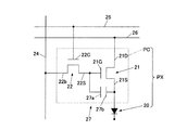
本発明の第1実施形態に係るエレクトロルミネッセンスパネルとして、ELディスプレイパネルを挙げて説明する。図1は、ELディスプレイパネル10における1つの画素PXの回路図である。このELディスプレイパネル10においては、赤、青及び緑の画素PXによって1ドットの画素が構成され、このような画素が表示領域全域にマトリクス状に配列されている。図1の水平方向の配列に着目すると赤の画素PX、青の画素PX、緑の画素PXの順に繰り返し配列され、図1の上下方向の配列に着目すると同じ色が一列に配列されている。
[First Embodiment]
An EL display panel will be described as an electroluminescence panel according to the first embodiment of the present invention. FIG. 1 is a circuit diagram of one pixel PX in the
このELディスプレイパネル10においては、画素PXに各種の信号を出力するために、複数の走査線25、信号線24及び供給線26が設けられている。走査線25と信号線24とは互いに直交する方向に延在している。
In the
画素PXは、2つのnチャネル型トランジスタ21,22と、キャパシタ27と、を有する画素回路PC及び有機EL素子20を有する。2つのnチャネル型トランジスタ21,22及びキャパシタ27は、走査線25、信号線24及び供給線26の入力信号に応じて有機EL素子20に電圧を印加する。
The pixel PX includes a pixel circuit PC and an
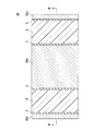
図2は1つの画素PXの平面図であり、図3は図2のIII−III矢視断面図である。図3に示すように、トランジスタアレイパネル50は、透明な基板2、ゲート絶縁膜31、画素回路PCを被覆する保護絶縁膜32を積層してなり、これらの間にキャパシタ27、走査線25、信号線24及び供給線26が形成されている。保護絶縁膜32はSiNx又はSiO2等を有している。
2 is a plan view of one pixel PX, and FIG. 3 is a cross-sectional view taken along the line III-III in FIG. As shown in FIG. 3, the
トランジスタアレイパネル50の上には、透明な導電体からなる画素電極20aがマトリクス状に形成されている。画素電極20aの厚さは50nm〜100nmである。画素電極20aは、ボトムエミッションの場合、錫ドープ酸化インジウム(Indium Tin Oxide;ITO)や酸化インジウムと酸化亜鉛の酸化物(Indium Zinc Oxide)、タングステンドープ酸化インジウム(Indium Tungsten Oxide;IWO)、タングステン−亜鉛ドープ酸化インジウム(Indium Tungsten Zinc Oxide;IWZO)等の透明電極材料を有し、トップエミッションの場合、上述の透明電極材料で形成された透明導電膜と、その下方にアルミ等の光反射性導電膜の積層構造である。
また、画素電極20aの外周部には、図2の水平方向及び上下方向の格子状に絶縁膜5が形成されている。絶縁膜5としては、例えばSiNx、又はSiO2等の無機絶縁膜を用いることができる。
On the
In addition, the
絶縁膜5は隔壁6の下地となる絶縁膜であり、図3に示すように、縦方向(基板2の面方向に直交する方向)の断面が略T字形状に形成されており、絶縁膜5の上面の辺の長さは、下面の辺の長さより長く、絶縁膜5の下部は画素電極20aから離れている。絶縁膜5の厚さは、画素電極20aの厚さと、後述する正孔注入層20bの厚さとを加えた厚さよりも充分に大きく、200nm〜600nmである。
The
絶縁膜5の上部には、同色の画素PXの配列方向に隔壁6が形成されている。隔壁6は、例えばポリイミド等の感光性樹脂により形成されたものであり、絶縁膜5の上面より幅狭に形成され、トランジスタ21,22の各電極、走査線25、信号線24及び供給線26よりも充分に厚い。隔壁6は、有機EL素子20を形成する際に異なる色の発光層20cとなる溶液が混合するのを防止する。また、隔壁6は、上部に形成される共通電極20dと、下部に配置されるトランジスタ21,22の各電極、走査線25、信号線24及び供給線26との容量結合を軽減する役割も果たす。
A
画素電極20a、絶縁膜5及び隔壁6の上部には、担体(キャリア)を輸送する第1担体輸送層として正孔注入層20bが形成されている。正孔注入層20bは、例えば酸化モリブデンや酸化ゲルマニウム等の無機酸化物を用いることができる。画素電極20a、絶縁膜5及び隔壁6が形成されたトランジスタアレイパネル50上に対して、全画素PX領域に対応する部位が開口しているハードマスクを設け、真空蒸着法、マグネットスパッタリング法等の気相堆積法により正孔注入層20bを全画素PX領域全域に形成することができる。正孔注入層20bの厚さは150nm以下であることが好ましい。
A
なお、絶縁膜5が充分に厚く、縦断面T字形状に形成され、画素電極20aと離れていること、さらに、気相堆積法は被蒸着物の指向性が高いことから絶縁膜5の下部近傍では絶縁膜5の上面が影になって、正孔注入層20bは、各画素PXごとに、隔壁6の表面や絶縁膜5の上面の周縁に形成された部分と、画素電極20aの上部に形成された部分とが分離して形成される。
Note that the
正孔注入層20bの上部には、第2担体輸送層として発光層20cが形成されている。発光層20cは、ポリフェニレンビニレン系発光材料やポリフルオレン系発光材料等の共役ポリマーからなる。なお、発光層20cの上にさらに電子輸送層を設けてもよい。また、これらの層構造において適切な層間に担体輸送を制限するインタレイヤ層が介在した積層構造であってもよいし、その他の積層構造であってもよい。
A
発光層20cは、湿式塗布法(例えば、発光層となる材料を含む液を個々の液滴を複数吐出するインクジェット法や、連続した液流として流すノズルコーティング法やその他印刷法)によって成膜される。この場合、発光層20cとなる共役ポリマー発光材料を含有する有機化合物含有液を塗布して成膜するが、厚膜の隔壁6が設けられているので、隣り合う画素電極20aに塗布された有機化合物含有液が隔壁6を越えて混ざり合うことを防止することができる。
なお、発光層20cは、図3に示すように、画素電極20aと絶縁膜5との隙間にも形成される。
The
The
なお、画素PXが赤の場合には発光層20cが赤色に発光し、画素PXが緑の場合には発光層20cが緑色に発光し、画素PXが青の場合には発光層20cが青色に発光するように、それぞれの材料を設定する。
The
発光層20c及び隔壁6の上には、有機EL素子20のカソードを構成する共通電極20dが成膜されている。共通電極20dは、全ての画素PXに共通して形成される。共通電極20dは、図示しないが、ボトムエミッションの場合、画素電極20aよりも仕事関数の低い材料(例えば、マグネシウム、カルシウム、リチウム、バリウム、希土類金属のうちの少なくとも一種を含む単体又は合金)の単層または複数層により1〜10nmの厚さに形成された電子注入層と、仕事関数の高い材料(例えばアルミニウム、クロム、銀やパラジウム銀系の合金等の導電性材料)を気相成長法によって100nm以上の厚さに成膜した導電層とからなり、トップエミッションの場合、上述の電子注入層と、その上方に積層された、錫ドープ酸化インジウム(Indium Tin Oxide;ITO)や酸化インジウムと酸化亜鉛の酸化物(Indium Zinc Oxide)、タングステンドープ酸化インジウム(Indium Tungsten Oxide;IWO)、タングステン−亜鉛ドープ酸化インジウム(Indium Tungsten Zinc Oxide;IWZO)等の透明電極材料で形成された透明導電膜と、を有している。
各画素毎に画素電極20a、正孔注入層20b、発光層20c、対向電極20dの順に積層されたものが有機EL素子20である。
On the
The
なお、図示しないが、対向電極20dの上には、封止層が堆積されている。封止層は有機EL素子20が外気に露出されることを防ぐ役割を果たす。封止層は、絶縁性を有し、例えば、エポキシ樹脂、アクリル樹脂等の熱硬化性樹脂、熱可塑性樹脂又は光硬化性樹脂等からなり、これらの樹脂にシリカ充填材等の添加剤を加えたものでもよい。
Although not shown, a sealing layer is deposited on the
次に、ELディスプレイパネル10の製造工程について図3〜図9を用いて説明する。
まず、図4に示すように、トランジスタアレイパネル50上に、画素電極20aの上面及び側面を被覆する犠牲層4を各画素電極20aごとに設ける。犠牲層4としては、例えばフォトレジストや、金属膜等を用いることができる。金属膜を用いる場合には、画素電極20aとの電池反応が促進されない金属材料であることが好ましい。そのような金属材料としては、例えばモリブデン(Mo)やクロム(Cr)等を用いることができる。
なお、格子状の絶縁膜5の形成領域には、犠牲層4を形成しない。
Next, the manufacturing process of the
First, as shown in FIG. 4, a
Note that the
次に、図5に示すように、トランジスタアレイパネル50上の全面に窒化シリコン又は酸化シリコン等の絶縁膜5Aを形成する。
次に、図6に示すように、絶縁膜5Aの上部のうち、犠牲層4の外周部と重なる部分、及び犠牲層4の間の部分を除く部分に、犠牲層7を形成する。犠牲層7としては、例えばフォトレジストや、金属膜等を用いることができる。
次に、ドライエッチング法により絶縁膜5Aをエッチングし、犠牲層7により覆われていない部分を除去することで、図7に示すように絶縁膜5を形成する。
Next, as shown in FIG. 5, an insulating
Next, as shown in FIG. 6, the
Next, the insulating
次に、図8に示すように、ウェットエッチングにより犠牲層7、犠牲層4を除去する。犠牲層7と犠牲層4ともに同一材料、またはエッチャントに対する溶解性が同等であれば、犠牲層7、犠牲層4をともに溶かす溶剤により同時に除去することができる。
Next, as shown in FIG. 8, the
次に、図3に示すように、絶縁膜5の上部にポリイミド等の感光性樹脂を硬化してなる隔壁6を形成してから、酸化モリブデンや酸化ゲルマニウム等の無機酸化物の蒸着又はスパッタを行い、隔壁6の表面及び画素電極20aの上部に、絶縁膜5の形状にしたがってそれぞれ互いに分離された正孔注入層20bを形成する。その後、隔壁6間の正孔注入層20b上に、ポリフェニレンビニレン系発光材料やポリフルオレン系発光材料等の共役ポリマーを含む溶液(懸濁液を含む)を塗布し、溶液中の溶媒を揮発させて正孔注入層20b上に発光層20cを堆積させる。塗布時の上記溶液は、液面が隔壁6の下面より高いために、乾燥すると一部が絶縁膜5の側壁及び隔壁6の側壁に付着することになる。この後、対向電極20dを複数の画素に跨るように表示領域全域に形成し、対向電極20dを覆うように封止層を形成する。以上により、ELディスプレイパネル10が完成する。
Next, as shown in FIG. 3, a
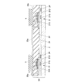
このようなELディスプレイパネル10において、図2、図3に示すように、隔壁6と正孔注入層20bとの界面において、正孔注入層20bに劣化Cが生じることがある。このような場合において、劣化Cの起点は隔壁6に接触する正孔注入層20bに生じる。
In such an
図9は劣化が進行した状態における1つの画素PXの平面図である。図9に示すように、隔壁6に接触する正孔注入層20bと、画素電極20a上の正孔注入層20bとが分離しているため、画素電極20a上の正孔注入層20bまで劣化Cが進行することはない。したがって、ダークスポットが生じることがなく、歩留まり率を向上させることができる。発光層20cのような正孔注入層20b以外の担体輸送層が画素電極20aから絶縁膜5の側壁及び隔壁6の側壁に連続して付着していても、劣化Cが、隔壁6に接触する正孔注入層20bにのみ生じるので、発光層20c等を介して画素電極20a上の正孔注入層20bに伝搬することはない。
FIG. 9 is a plan view of one pixel PX in a state where deterioration has progressed. As shown in FIG. 9, since the
なお、本発明は、トップエミッション型、ボトムエミッション型のいずれのELディスプレイパネルにも適用可能である。また、本発明は、ELディスプレイパネルに限られず、例えば、露光装置、光アドレッシング装置、照明装置等のエレクトロルミネッセンスパネルに適用してもよい。
また上記実施形態では、隔壁6は、図10(a)に示すように、異なる色の画素PX間に配置されるストライプ形状でもよく、また図10(b)に示すように、各画素PX毎に周囲を包囲するように行方向及び列方向に格子状に形成されてもよい。
Note that the present invention can be applied to both a top emission type and a bottom emission type EL display panel. Further, the present invention is not limited to an EL display panel, and may be applied to an electroluminescence panel such as an exposure apparatus, an optical addressing apparatus, and an illumination apparatus.
Further, in the above-described embodiment, the
5 絶縁膜
6 隔壁
10 ELディスプレイパネル
20 有機EL素子
20a 画素電極
20b 正孔注入層
20c 発光層
20d 共通電極(対向電極)
5 Insulating
Claims (1)
前記複数の第1電極を被覆する犠牲層を設け、
前記犠牲層の周囲と重なる位置に、前記犠牲層よりも高い絶縁膜を設け、
前記犠牲層を除去して、前記絶縁膜の上端を前記絶縁膜の下端よりも前記第1電極側へ突出させ、
前記絶縁膜の上部に隔壁を設け、
前記第1電極及び前記隔壁の上部に、それぞれ互いに分離するように前記複数の担体輸送層のうちの第1担体輸送層を形成することを特徴とするエレクトロルミネッセンスパネルの製造方法。 In a method for manufacturing an electroluminescence panel having a plurality of carrier transport layers between a plurality of first electrodes and a second electrode formed on a substrate,
Providing a sacrificial layer covering the plurality of first electrodes;
An insulating film higher than the sacrificial layer is provided at a position overlapping the periphery of the sacrificial layer,
Removing the sacrificial layer, causing the upper end of the insulating film to protrude toward the first electrode from the lower end of the insulating film;
A partition is provided on the insulating film,
A method of manufacturing an electroluminescence panel, wherein a first carrier transport layer of the plurality of carrier transport layers is formed on the first electrode and the partition so as to be separated from each other .
Priority Applications (1)
| Application Number | Priority Date | Filing Date | Title |
|---|---|---|---|
| JP2008206781A JP5077136B2 (en) | 2008-08-11 | 2008-08-11 | Method for manufacturing electroluminescence panel |
Applications Claiming Priority (1)
| Application Number | Priority Date | Filing Date | Title |
|---|---|---|---|
| JP2008206781A JP5077136B2 (en) | 2008-08-11 | 2008-08-11 | Method for manufacturing electroluminescence panel |
Publications (3)
| Publication Number | Publication Date |
|---|---|
| JP2010044902A JP2010044902A (en) | 2010-02-25 |
| JP2010044902A5 JP2010044902A5 (en) | 2011-05-12 |
| JP5077136B2 true JP5077136B2 (en) | 2012-11-21 |
Family
ID=42016141
Family Applications (1)
| Application Number | Title | Priority Date | Filing Date |
|---|---|---|---|
| JP2008206781A Expired - Fee Related JP5077136B2 (en) | 2008-08-11 | 2008-08-11 | Method for manufacturing electroluminescence panel |
Country Status (1)
| Country | Link |
|---|---|
| JP (1) | JP5077136B2 (en) |
Families Citing this family (2)
| Publication number | Priority date | Publication date | Assignee | Title |
|---|---|---|---|---|
| JP5625448B2 (en) * | 2010-03-31 | 2014-11-19 | 凸版印刷株式会社 | Method for manufacturing organic EL element and organic EL image display device |
| JP2018129471A (en) | 2017-02-10 | 2018-08-16 | 株式会社Joled | Organic electroluminescent panel and light emitting device |
Family Cites Families (4)
| Publication number | Priority date | Publication date | Assignee | Title |
|---|---|---|---|---|
| JP4718768B2 (en) * | 2003-09-19 | 2011-07-06 | 株式会社半導体エネルギー研究所 | Light emitting device |
| JP2006310289A (en) * | 2005-03-31 | 2006-11-09 | Seiko Epson Corp | Light emitting device, method of manufacturing the same, and electronic apparatus |
| JP2007103164A (en) * | 2005-10-04 | 2007-04-19 | Tohoku Pioneer Corp | Self-luminous panel and method of manufacturing self-luminous panel |
| JP5087837B2 (en) * | 2005-12-15 | 2012-12-05 | 大日本印刷株式会社 | Color filter for organic electroluminescence device |
-
2008
- 2008-08-11 JP JP2008206781A patent/JP5077136B2/en not_active Expired - Fee Related
Also Published As
| Publication number | Publication date |
|---|---|
| JP2010044902A (en) | 2010-02-25 |
Similar Documents
| Publication | Publication Date | Title |
|---|---|---|
| JP5476878B2 (en) | Manufacturing method of light emitting panel | |
| US10854839B2 (en) | Organic el display panel and method of manufacturing organic el display panel | |
| JP6688701B2 (en) | Organic EL display panel and method for manufacturing organic EL display panel | |
| CN111293152B (en) | Display substrate, preparation method thereof and electroluminescent display device | |
| JP2005327674A (en) | Organic electroluminescent display element, display device having the same, and manufacturing method thereof | |
| JP2007188862A (en) | Organic el light-emitting device and its manufacturing method | |
| CN108417600B (en) | Organic EL display panel and method for manufacturing organic EL display panel | |
| JP2009238456A (en) | Electroluminescence panel | |
| WO2006064715A1 (en) | Display device and display device manufacturing method | |
| JP2011119212A (en) | Method for manufacturing organic el device, organic el device, and electronic apparatus | |
| CN112640579A (en) | Display device | |
| JP4937935B2 (en) | Organic EL display and method for manufacturing organic EL display | |
| JP2009092908A (en) | Display apparatus and method of producing the same | |
| JP2010056025A (en) | Light emitting panel, and method of manufacturing light emitting panel | |
| JP5077136B2 (en) | Method for manufacturing electroluminescence panel | |
| JP4848675B2 (en) | Transistor array panel and method of manufacturing transistor array panel | |
| JP2006004743A (en) | Display device and its manufacturing method | |
| JP5267845B2 (en) | Manufacturing method of display device | |
| JP2009070704A (en) | Display device and its manufacturing method | |
| JP2020030933A (en) | Organic el display panel and manufacturing method of organic el display panel | |
| KR100592388B1 (en) | Organic electroluminescent display device and manufacturing method thereof | |
| JP2010191368A (en) | Display panel and method for manufacturing the same | |
| JP2018156882A (en) | Organic el display panel and manufacturing method thereof | |
| JP4998412B2 (en) | Method for manufacturing electroluminescence panel | |
| JP2012058664A (en) | Light-emitting panel, and manufacturing method of light-emitting panel |
Legal Events
| Date | Code | Title | Description |
|---|---|---|---|
| A521 | Request for written amendment filed |
Free format text: JAPANESE INTERMEDIATE CODE: A523 Effective date: 20110325 |
|
| A621 | Written request for application examination |
Free format text: JAPANESE INTERMEDIATE CODE: A621 Effective date: 20110325 |
|
| RD02 | Notification of acceptance of power of attorney |
Free format text: JAPANESE INTERMEDIATE CODE: A7422 Effective date: 20110325 |
|
| A977 | Report on retrieval |
Free format text: JAPANESE INTERMEDIATE CODE: A971007 Effective date: 20120314 |
|
| A131 | Notification of reasons for refusal |
Free format text: JAPANESE INTERMEDIATE CODE: A131 Effective date: 20120508 |
|
| A521 | Request for written amendment filed |
Free format text: JAPANESE INTERMEDIATE CODE: A523 Effective date: 20120709 |
|
| TRDD | Decision of grant or rejection written | ||
| A01 | Written decision to grant a patent or to grant a registration (utility model) |
Free format text: JAPANESE INTERMEDIATE CODE: A01 Effective date: 20120731 |
|
| A01 | Written decision to grant a patent or to grant a registration (utility model) |
Free format text: JAPANESE INTERMEDIATE CODE: A01 |
|
| A61 | First payment of annual fees (during grant procedure) |
Free format text: JAPANESE INTERMEDIATE CODE: A61 Effective date: 20120813 |
|
| FPAY | Renewal fee payment (event date is renewal date of database) |
Free format text: PAYMENT UNTIL: 20150907 Year of fee payment: 3 |
|
| R150 | Certificate of patent or registration of utility model |
Ref document number: 5077136 Country of ref document: JP Free format text: JAPANESE INTERMEDIATE CODE: R150 Free format text: JAPANESE INTERMEDIATE CODE: R150 |
|
| R250 | Receipt of annual fees |
Free format text: JAPANESE INTERMEDIATE CODE: R250 |
|
| S111 | Request for change of ownership or part of ownership |
Free format text: JAPANESE INTERMEDIATE CODE: R313113 |
|
| R350 | Written notification of registration of transfer |
Free format text: JAPANESE INTERMEDIATE CODE: R350 |
|
| R250 | Receipt of annual fees |
Free format text: JAPANESE INTERMEDIATE CODE: R250 |
|
| R250 | Receipt of annual fees |
Free format text: JAPANESE INTERMEDIATE CODE: R250 |
|
| R250 | Receipt of annual fees |
Free format text: JAPANESE INTERMEDIATE CODE: R250 |
|
| LAPS | Cancellation because of no payment of annual fees |