JP5269770B2 - In-situ cleaning of CVD system discharge - Google Patents
In-situ cleaning of CVD system discharge Download PDFInfo
- Publication number
- JP5269770B2 JP5269770B2 JP2009511203A JP2009511203A JP5269770B2 JP 5269770 B2 JP5269770 B2 JP 5269770B2 JP 2009511203 A JP2009511203 A JP 2009511203A JP 2009511203 A JP2009511203 A JP 2009511203A JP 5269770 B2 JP5269770 B2 JP 5269770B2
- Authority
- JP
- Japan
- Prior art keywords
- chamber
- low frequency
- gas
- reaction chamber
- exhaust line
- Prior art date
- Legal status (The legal status is an assumption and is not a legal conclusion. Google has not performed a legal analysis and makes no representation as to the accuracy of the status listed.)
- Expired - Fee Related
Links
- 238000004140 cleaning Methods 0.000 title description 40
- 238000011065 in-situ storage Methods 0.000 title description 2
- 239000007789 gas Substances 0.000 claims description 58
- 238000000034 method Methods 0.000 claims description 52
- 229920000642 polymer Polymers 0.000 claims description 46
- 238000006243 chemical reaction Methods 0.000 claims description 28
- 230000015572 biosynthetic process Effects 0.000 claims description 20
- 239000000460 chlorine Substances 0.000 claims description 15
- 229910052801 chlorine Inorganic materials 0.000 claims description 10
- 239000006227 byproduct Substances 0.000 claims description 9
- ZAMOUSCENKQFHK-UHFFFAOYSA-N Chlorine atom Chemical compound [Cl] ZAMOUSCENKQFHK-UHFFFAOYSA-N 0.000 claims description 8
- 239000000758 substrate Substances 0.000 claims description 7
- 239000005046 Chlorosilane Substances 0.000 claims description 6
- KOPOQZFJUQMUML-UHFFFAOYSA-N chlorosilane Chemical compound Cl[SiH3] KOPOQZFJUQMUML-UHFFFAOYSA-N 0.000 claims description 6
- 238000009826 distribution Methods 0.000 claims description 3
- 230000001939 inductive effect Effects 0.000 claims 2
- 238000012545 processing Methods 0.000 description 32
- 238000000151 deposition Methods 0.000 description 24
- 238000005229 chemical vapour deposition Methods 0.000 description 21
- 230000008021 deposition Effects 0.000 description 21
- 239000000463 material Substances 0.000 description 21
- 230000002265 prevention Effects 0.000 description 20
- 241000894007 species Species 0.000 description 17
- 238000009825 accumulation Methods 0.000 description 9
- 239000004065 semiconductor Substances 0.000 description 9
- VYPSYNLAJGMNEJ-UHFFFAOYSA-N Silicium dioxide Chemical compound O=[Si]=O VYPSYNLAJGMNEJ-UHFFFAOYSA-N 0.000 description 8
- 239000000047 product Substances 0.000 description 7
- 239000010453 quartz Substances 0.000 description 7
- 239000013618 particulate matter Substances 0.000 description 6
- 238000010438 heat treatment Methods 0.000 description 5
- 239000007788 liquid Substances 0.000 description 5
- PXHVJJICTQNCMI-UHFFFAOYSA-N Nickel Chemical compound [Ni] PXHVJJICTQNCMI-UHFFFAOYSA-N 0.000 description 4
- 230000006378 damage Effects 0.000 description 4
- 239000010408 film Substances 0.000 description 4
- 239000011261 inert gas Substances 0.000 description 4
- 238000006116 polymerization reaction Methods 0.000 description 4
- 239000000843 powder Substances 0.000 description 4
- IJGRMHOSHXDMSA-UHFFFAOYSA-N Atomic nitrogen Chemical compound N#N IJGRMHOSHXDMSA-UHFFFAOYSA-N 0.000 description 3
- YCKRFDGAMUMZLT-UHFFFAOYSA-N Fluorine atom Chemical compound [F] YCKRFDGAMUMZLT-UHFFFAOYSA-N 0.000 description 3
- 238000013459 approach Methods 0.000 description 3
- 239000000919 ceramic Substances 0.000 description 3
- 150000001875 compounds Chemical class 0.000 description 3
- 238000005530 etching Methods 0.000 description 3
- 229910052731 fluorine Inorganic materials 0.000 description 3
- 239000011737 fluorine Substances 0.000 description 3
- 238000005268 plasma chemical vapour deposition Methods 0.000 description 3
- 239000000376 reactant Substances 0.000 description 3
- 239000011343 solid material Substances 0.000 description 3
- 229910001220 stainless steel Inorganic materials 0.000 description 3
- 239000010935 stainless steel Substances 0.000 description 3
- QGZKDVFQNNGYKY-UHFFFAOYSA-N Ammonia Chemical compound N QGZKDVFQNNGYKY-UHFFFAOYSA-N 0.000 description 2
- RYGMFSIKBFXOCR-UHFFFAOYSA-N Copper Chemical compound [Cu] RYGMFSIKBFXOCR-UHFFFAOYSA-N 0.000 description 2
- 229910052581 Si3N4 Inorganic materials 0.000 description 2
- XUIMIQQOPSSXEZ-UHFFFAOYSA-N Silicon Chemical compound [Si] XUIMIQQOPSSXEZ-UHFFFAOYSA-N 0.000 description 2
- 239000011248 coating agent Substances 0.000 description 2
- 238000000576 coating method Methods 0.000 description 2
- 239000000356 contaminant Substances 0.000 description 2
- 229910052802 copper Inorganic materials 0.000 description 2
- 239000010949 copper Substances 0.000 description 2
- 238000010494 dissociation reaction Methods 0.000 description 2
- 230000005593 dissociations Effects 0.000 description 2
- 239000001257 hydrogen Substances 0.000 description 2
- 229910052739 hydrogen Inorganic materials 0.000 description 2
- 229910052751 metal Inorganic materials 0.000 description 2
- 239000002184 metal Substances 0.000 description 2
- 238000012986 modification Methods 0.000 description 2
- 230000004048 modification Effects 0.000 description 2
- 229910052759 nickel Inorganic materials 0.000 description 2
- 239000012071 phase Substances 0.000 description 2
- 238000001020 plasma etching Methods 0.000 description 2
- 239000002243 precursor Substances 0.000 description 2
- 238000010926 purge Methods 0.000 description 2
- 230000005855 radiation Effects 0.000 description 2
- 229910052710 silicon Inorganic materials 0.000 description 2
- 239000010703 silicon Substances 0.000 description 2
- HQVNEWCFYHHQES-UHFFFAOYSA-N silicon nitride Chemical compound N12[Si]34N5[Si]62N3[Si]51N64 HQVNEWCFYHHQES-UHFFFAOYSA-N 0.000 description 2
- 239000007787 solid Substances 0.000 description 2
- 239000000126 substance Substances 0.000 description 2
- OKTJSMMVPCPJKN-UHFFFAOYSA-N Carbon Chemical compound [C] OKTJSMMVPCPJKN-UHFFFAOYSA-N 0.000 description 1
- KZBUYRJDOAKODT-UHFFFAOYSA-N Chlorine Chemical compound ClCl KZBUYRJDOAKODT-UHFFFAOYSA-N 0.000 description 1
- UFHFLCQGNIYNRP-UHFFFAOYSA-N Hydrogen Chemical compound [H][H] UFHFLCQGNIYNRP-UHFFFAOYSA-N 0.000 description 1
- BLRPTPMANUNPDV-UHFFFAOYSA-N Silane Chemical compound [SiH4] BLRPTPMANUNPDV-UHFFFAOYSA-N 0.000 description 1
- 229910000831 Steel Inorganic materials 0.000 description 1
- 230000002411 adverse Effects 0.000 description 1
- 229910052782 aluminium Inorganic materials 0.000 description 1
- XAGFODPZIPBFFR-UHFFFAOYSA-N aluminium Chemical compound [Al] XAGFODPZIPBFFR-UHFFFAOYSA-N 0.000 description 1
- -1 aluminum or steel Chemical class 0.000 description 1
- 229910021529 ammonia Inorganic materials 0.000 description 1
- 239000007795 chemical reaction product Substances 0.000 description 1
- 239000004020 conductor Substances 0.000 description 1
- 239000000470 constituent Substances 0.000 description 1
- 238000010276 construction Methods 0.000 description 1
- 238000000354 decomposition reaction Methods 0.000 description 1
- 238000005137 deposition process Methods 0.000 description 1
- 238000013461 design Methods 0.000 description 1
- PZPGRFITIJYNEJ-UHFFFAOYSA-N disilane Chemical compound [SiH3][SiH3] PZPGRFITIJYNEJ-UHFFFAOYSA-N 0.000 description 1
- KPUWHANPEXNPJT-UHFFFAOYSA-N disiloxane Chemical class [SiH3]O[SiH3] KPUWHANPEXNPJT-UHFFFAOYSA-N 0.000 description 1
- 238000005516 engineering process Methods 0.000 description 1
- 239000002360 explosive Substances 0.000 description 1
- 239000010419 fine particle Substances 0.000 description 1
- 125000001153 fluoro group Chemical group F* 0.000 description 1
- 239000010795 gaseous waste Substances 0.000 description 1
- PCHJSUWPFVWCPO-UHFFFAOYSA-N gold Chemical compound [Au] PCHJSUWPFVWCPO-UHFFFAOYSA-N 0.000 description 1
- 229910052737 gold Inorganic materials 0.000 description 1
- 239000010931 gold Substances 0.000 description 1
- 229910002804 graphite Inorganic materials 0.000 description 1
- 239000010439 graphite Substances 0.000 description 1
- 239000002920 hazardous waste Substances 0.000 description 1
- 150000002431 hydrogen Chemical class 0.000 description 1
- 230000006698 induction Effects 0.000 description 1
- 238000010849 ion bombardment Methods 0.000 description 1
- 238000002955 isolation Methods 0.000 description 1
- 239000011344 liquid material Substances 0.000 description 1
- 238000004519 manufacturing process Methods 0.000 description 1
- 238000003913 materials processing Methods 0.000 description 1
- 239000012528 membrane Substances 0.000 description 1
- 150000002739 metals Chemical class 0.000 description 1
- QKCGXXHCELUCKW-UHFFFAOYSA-N n-[4-[4-(dinaphthalen-2-ylamino)phenyl]phenyl]-n-naphthalen-2-ylnaphthalen-2-amine Chemical compound C1=CC=CC2=CC(N(C=3C=CC(=CC=3)C=3C=CC(=CC=3)N(C=3C=C4C=CC=CC4=CC=3)C=3C=C4C=CC=CC4=CC=3)C3=CC4=CC=CC=C4C=C3)=CC=C21 QKCGXXHCELUCKW-UHFFFAOYSA-N 0.000 description 1
- 229910052757 nitrogen Inorganic materials 0.000 description 1
- 239000002245 particle Substances 0.000 description 1
- 230000000737 periodic effect Effects 0.000 description 1
- 238000005240 physical vapour deposition Methods 0.000 description 1
- 229910021420 polycrystalline silicon Inorganic materials 0.000 description 1
- 239000002861 polymer material Substances 0.000 description 1
- 229920005591 polysilicon Polymers 0.000 description 1
- 239000012495 reaction gas Substances 0.000 description 1
- 229910000077 silane Inorganic materials 0.000 description 1
- LIVNPJMFVYWSIS-UHFFFAOYSA-N silicon monoxide Chemical compound [Si-]#[O+] LIVNPJMFVYWSIS-UHFFFAOYSA-N 0.000 description 1
- 229910052814 silicon oxide Inorganic materials 0.000 description 1
- 239000007790 solid phase Substances 0.000 description 1
- 239000002910 solid waste Substances 0.000 description 1
- 239000010959 steel Substances 0.000 description 1
- 238000002230 thermal chemical vapour deposition Methods 0.000 description 1
- 239000010409 thin film Substances 0.000 description 1
- 238000011144 upstream manufacturing Methods 0.000 description 1
- 238000001771 vacuum deposition Methods 0.000 description 1
- 239000011345 viscous material Substances 0.000 description 1
- XLYOFNOQVPJJNP-UHFFFAOYSA-N water Substances O XLYOFNOQVPJJNP-UHFFFAOYSA-N 0.000 description 1
Images


Classifications
-
- H—ELECTRICITY
- H01—ELECTRIC ELEMENTS
- H01J—ELECTRIC DISCHARGE TUBES OR DISCHARGE LAMPS
- H01J37/00—Discharge tubes with provision for introducing objects or material to be exposed to the discharge, e.g. for the purpose of examination or processing thereof
- H01J37/32—Gas-filled discharge tubes
- H01J37/32431—Constructional details of the reactor
- H01J37/3244—Gas supply means
-
- C—CHEMISTRY; METALLURGY
- C23—COATING METALLIC MATERIAL; COATING MATERIAL WITH METALLIC MATERIAL; CHEMICAL SURFACE TREATMENT; DIFFUSION TREATMENT OF METALLIC MATERIAL; COATING BY VACUUM EVAPORATION, BY SPUTTERING, BY ION IMPLANTATION OR BY CHEMICAL VAPOUR DEPOSITION, IN GENERAL; INHIBITING CORROSION OF METALLIC MATERIAL OR INCRUSTATION IN GENERAL
- C23C—COATING METALLIC MATERIAL; COATING MATERIAL WITH METALLIC MATERIAL; SURFACE TREATMENT OF METALLIC MATERIAL BY DIFFUSION INTO THE SURFACE, BY CHEMICAL CONVERSION OR SUBSTITUTION; COATING BY VACUUM EVAPORATION, BY SPUTTERING, BY ION IMPLANTATION OR BY CHEMICAL VAPOUR DEPOSITION, IN GENERAL
- C23C16/00—Chemical coating by decomposition of gaseous compounds, without leaving reaction products of surface material in the coating, i.e. chemical vapour deposition [CVD] processes
- C23C16/44—Chemical coating by decomposition of gaseous compounds, without leaving reaction products of surface material in the coating, i.e. chemical vapour deposition [CVD] processes characterised by the method of coating
- C23C16/4412—Details relating to the exhausts, e.g. pumps, filters, scrubbers, particle traps
-
- H—ELECTRICITY
- H01—ELECTRIC ELEMENTS
- H01L—SEMICONDUCTOR DEVICES NOT COVERED BY CLASS H10
- H01L21/00—Processes or apparatus adapted for the manufacture or treatment of semiconductor or solid state devices or of parts thereof
- H01L21/02—Manufacture or treatment of semiconductor devices or of parts thereof
- H01L21/02104—Forming layers
- H01L21/02107—Forming insulating materials on a substrate
- H01L21/02296—Forming insulating materials on a substrate characterised by the treatment performed before or after the formation of the layer
- H01L21/02299—Forming insulating materials on a substrate characterised by the treatment performed before or after the formation of the layer pre-treatment
- H01L21/02301—Forming insulating materials on a substrate characterised by the treatment performed before or after the formation of the layer pre-treatment in-situ cleaning
Landscapes
- Chemical & Material Sciences (AREA)
- Engineering & Computer Science (AREA)
- General Chemical & Material Sciences (AREA)
- Chemical Kinetics & Catalysis (AREA)
- Materials Engineering (AREA)
- Mechanical Engineering (AREA)
- Metallurgy (AREA)
- Organic Chemistry (AREA)
- Physics & Mathematics (AREA)
- Plasma & Fusion (AREA)
- Analytical Chemistry (AREA)
- Condensed Matter Physics & Semiconductors (AREA)
- General Physics & Mathematics (AREA)
- Manufacturing & Machinery (AREA)
- Computer Hardware Design (AREA)
- Microelectronics & Electronic Packaging (AREA)
- Power Engineering (AREA)
- Drying Of Semiconductors (AREA)
- Chemical Vapour Deposition (AREA)
Description
[0001]本発明の実施形態は概して、化学気相堆積(CVD)排出システムの洗浄に、より具体的には、CVDシステムにおけるポリマー汚染物のイン・シトゥー洗浄に関する。 [0001] Embodiments of the present invention generally relate to cleaning chemical vapor deposition (CVD) exhaust systems, and more specifically to in situ cleaning of polymer contaminants in CVD systems.
[0002]CVD処理時、堆積ガスは処理チャンバ内で開放され、処理中の基板の表面上に薄膜層を形成する。処理チャンバの壁などのエリアへの不要な堆積はまたこのようなCVDプロセス時に生じる。しかしながら、これらの堆積ガスの個別分子のチャンバへの常駐時間は比較的短いため、チャンバに開放された分子のごくわずかのみが堆積プロセスで消費され、またウェーハやチャンバ壁のいずれかに堆積される。 [0002] During CVD processing, the deposition gas is released in the processing chamber, forming a thin film layer on the surface of the substrate being processed. Unnecessary deposition on areas such as processing chamber walls also occurs during such CVD processes. However, the residence time of individual molecules of these deposition gases in the chamber is relatively short so that only a small percentage of the molecules open to the chamber are consumed in the deposition process and are deposited either on the wafer or on the chamber walls. .
[0003]ウェーハ上に層を形成するためにCVDが利用される半導体製造プロセス時には、注入されたプロセスガスがウェーハ基板表面のみに堆積するとしても、実際は、一部のガス分子は基板表面を外れて、プロセスチャンバ表面に堆積することが理想的であろう。消費されなかったガス分子の一部は、真空の排出ラインを介して部分反応化合物および反応副生成物と共にチャンバ外にポンピングされる。この排出ガスにおける化合物の多くは依然として高反応性状態であり、および/または排出ラインに不要な堆積物を形成する恐れのある残渣や微粒子物質を含有している。Applied Materialsによって製造されたEpi Centura(登録商標)チャンバなどの処理チャンバにおいて、プロセスガスの温度は、プロセスガスが排出ラインに入るのに伴って処理チャンバからの出口において大きく低下し、排出インサート、排出キャップおよび排出ラインの少なくとも最初の4フィートのコーティングをもたらす。上記材料に加えて、このコーティングは、蜂蜜のような濃度の、概して半透明な粘性液体であると観察された。濃縮された排出副生成物はまた、プロセス条件および排出ラインの場所に応じて、不透明な白色から不透明な黄色、そして不透明な赤茶色に見えることがある。濃縮された排出副生成物が不透明である場合、これは固相にあるように見える。半透明な液体は大気への曝露時に即時に反応して不透明な白色材料を形成すると考えられる。 [0003] During semiconductor manufacturing processes where CVD is used to form layers on the wafer, some gas molecules actually deviate from the substrate surface, even though the injected process gas only deposits on the wafer substrate surface. It would be ideal to deposit on the process chamber surface. Some of the gas molecules that have not been consumed are pumped out of the chamber along with the partially reacted compounds and reaction byproducts via a vacuum exhaust line. Many of the compounds in this exhaust gas are still highly reactive and / or contain residues and particulate matter that can form unwanted deposits in the exhaust line. In processing chambers such as Epi Centura® chambers manufactured by Applied Materials, the temperature of the process gas is greatly reduced at the outlet from the processing chamber as the process gas enters the discharge line, and the exhaust insert, exhaust Provide at least the first 4 feet of coating on the cap and discharge line. In addition to the above materials, the coating was observed to be a honey-like concentration, generally a translucent viscous liquid. Concentrated discharge by-products can also appear from an opaque white to an opaque yellow and an opaque red-brown depending on the process conditions and the location of the discharge line. If the concentrated effluent byproduct is opaque, it appears to be in the solid phase. The translucent liquid is thought to react immediately upon exposure to the atmosphere to form an opaque white material.
[0004]したがって、排出ラインにおける液体および固体材料の集積は複数の問題を提起する。第1に、この集積は、この材料がしばしば、標準的な定期洗浄動作時に真空シールが破壊され、かつ排出ラインが大気条件に曝露される場合に着火する可能性がある自然発火性物質である点において安全性に対する危険を提起する。第2に、堆積材料の多くが排出ラインに集積すると、排出ラインおよび/またはこの関連真空ポンプは、適切に洗浄されていないと詰まる場合がある。定期的に洗浄されていても、物質の集積は真空ポンプの正常動作と干渉して、ポンプの耐用年数を大きく短縮する恐れがある。また、固体物質は排出ラインから処理チャンバに逆流して処理チャンバを汚染する場合がある。半透明な液体が急速に空気に曝露されると、爆発反応が生じる恐れがある。 [0004] Thus, the accumulation of liquid and solid materials in the discharge line poses several problems. First, this accumulation is a pyrophoric material that can often ignite if the vacuum seal is broken during standard periodic cleaning operations and the exhaust line is exposed to atmospheric conditions. Poses a safety hazard in terms of Second, as much of the deposited material accumulates in the exhaust line, the exhaust line and / or this associated vacuum pump may become clogged if not properly cleaned. Even if cleaned regularly, the accumulation of material can interfere with the normal operation of the vacuum pump and can greatly shorten the useful life of the pump. Also, the solid material may flow back from the discharge line to the processing chamber and contaminate the processing chamber. If a translucent liquid is rapidly exposed to air, an explosive reaction may occur.
[0005]これらの問題を回避するために、排出ラインの内部表面は、堆積材料を除去するために規則的に洗浄される。この手順は、チャンバ壁および処理チャンバの類似エリアから不要な堆積材料を除去するために用いられる標準的なチャンバ洗浄動作時に実行される。一般的なチャンバ洗浄技術は、チャンバ壁および他のエリアから堆積材料を除去するために、フッ素などのエッチングガスを使用することを含んでいる。エッチングガスはチャンバに導入されてプラズマが形成され、エッチングガスは堆積材料と反応して、これをチャンバ壁から除去する。このような洗浄手順は一般的に、各ウェーハまたは多数のウェーハの堆積ステップの間に実行される。 [0005] To avoid these problems, the internal surface of the exhaust line is regularly cleaned to remove the deposited material. This procedure is performed during a standard chamber cleaning operation used to remove unwanted deposition material from the chamber walls and similar areas of the processing chamber. A typical chamber cleaning technique involves using an etching gas such as fluorine to remove deposited material from the chamber walls and other areas. Etching gas is introduced into the chamber to form a plasma, which reacts with the deposited material and removes it from the chamber walls. Such cleaning procedures are typically performed during each wafer or multiple wafer deposition step.
[0006]チャンバ壁からの堆積材料の除去は、堆積材料に近接したエリアにおいてチャンバ内にプラズマが作成される点においては比較的単純である。排出ラインからの堆積材料の除去は、排出ラインが処理チャンバの下流にあるため、より困難である。固定周期において、処理チャンバ内の多数のポイントは、排出ライン内のポイントよりも多くのエッチャントフッ素原子に接触するようになる。したがって、固定周期においては、チャンバは洗浄プロセスによって適切に洗浄可能であるが、残渣および類似の堆積物は排出ラインに残っている。 [0006] Removal of deposited material from the chamber walls is relatively simple in that a plasma is created in the chamber in an area proximate to the deposited material. Removal of deposited material from the exhaust line is more difficult because the exhaust line is downstream of the processing chamber. In a fixed cycle, many points in the processing chamber come into contact with more etchant fluorine atoms than points in the discharge line. Thus, in a fixed cycle, the chamber can be properly cleaned by the cleaning process, but residues and similar deposits remain in the discharge line.
[0007]排出ラインの適切な洗浄を試みるためには、洗浄動作の期間は増加されるべきである。しかしながら、洗浄動作の長さの増加は、機器のダウンタイムを招くため望ましくなく、これはウェーハスループットに悪影響を与える。また、このような残渣集積は、洗浄プロセスによる反応物が、排出ラインの残渣と反応可能な状態で排出ラインに排出される程度にのみ洗浄可能である。一部のシステムおよび用途において、排出反応物の常駐時間では、排出ラインの終了ポイントまたは中間ポイントに至るのも不十分である。これらのシステムおよび用途において、残渣集積はより大きな関心事である。 [0007] In order to attempt proper cleaning of the drain line, the duration of the cleaning operation should be increased. However, increasing the length of the cleaning operation is undesirable because it results in equipment downtime, which adversely affects wafer throughput. Further, such residue accumulation can be cleaned only to the extent that the reactants from the cleaning process are discharged to the discharge line in a state where they can react with the residue in the discharge line. In some systems and applications, the residence time of the exhaust reactant is not sufficient to reach the end or middle point of the exhaust line. In these systems and applications, residue accumulation is a greater concern.
[0008]複数の異なるデバイスが、このような排出ラインの洗浄を容易にするために設計されてきた。排出ラインを洗浄するために用いられてきたアプローチの1つは、微粒子物質が容易に逃げられない収集チャンバにガス流を送出することによって、排出ストリームにある微粒子物質を真空ポンプに至る前にトラップすることである。この技術に依存するデバイスは、除去可能なドアや類似のアクセスを収集チャンバに提供するため、十分な量の材料がチャンバ内に集積すると、容易に除去可能である。通常、基板堆積システムは、収集チャンバが洗浄される期間は一時的にシャットオフされ、システムのウェーハスループットを制限または低減させる。 [0008] A number of different devices have been designed to facilitate cleaning of such drain lines. One approach that has been used to clean the exhaust line is to trap particulate matter in the exhaust stream before it reaches the vacuum pump by delivering a gas stream to a collection chamber where the particulate matter cannot easily escape. It is to be. Devices that rely on this technology provide a removable door or similar access to the collection chamber and can be easily removed once a sufficient amount of material has accumulated in the chamber. Typically, the substrate deposition system is temporarily shut off during the time the collection chamber is cleaned, limiting or reducing the wafer throughput of the system.
[0009]排出ラインを洗浄するために用いられてきたアプローチの1つは、膜が電極表面に堆積する際に排出ガスの反応成分を抽出するためにプラズマCVD技術を使用するスクラブシステムに依存する。スクラブシステムは、固体膜である反応物の除去を最大化するように設計されており、また表面積の大きなスパイラル電極を使用する。スパイラル電極は、送風ポンプと機械ポンプ間の排出ラインの終端付近に位置決めされている除去可能なキャニスター内に含有されている。十分な量の固体廃棄物が電極に集積すると、キャニスターは廃棄および置換のために除去されてもよい。 [0009] One approach that has been used to clean the exhaust line relies on a scrub system that uses plasma CVD techniques to extract the reactive components of the exhaust gas as the film is deposited on the electrode surface. . The scrub system is designed to maximize the removal of reactants that are solid membranes, and uses a high surface area spiral electrode. The spiral electrode is contained in a removable canister positioned near the end of the discharge line between the blower pump and the mechanical pump. Once a sufficient amount of solid waste has accumulated on the electrode, the canister may be removed for disposal and replacement.
[0010]収集する堆積固体物質用のエリアを提供するために電極の表面積の多くにシステムが依存している点において、この従来技術の方法には複数の問題がある。電極の表面積の多くを収容するために、システムは必然的に大きくかさばる。さらに、除去可能なキャニスターは、置換されて適切に廃棄されるべき使い捨て製品であるため、従来技術のスクラブシステムの動作には余分な費用がかかる。また、スクラブシステムは真空排出ラインの開始部分の下流に配置されているため、ラインのこの部分に集積する粉末材料や微粒子物質の除去を保証しない。 [0010] This prior art method has several problems in that the system relies on much of the surface area of the electrode to provide an area for the deposited solid material to collect. In order to accommodate much of the electrode surface area, the system is necessarily bulky and bulky. In addition, since the removable canister is a disposable product that must be replaced and properly disposed of, the operation of the prior art scrub system is costly. Also, because the scrub system is located downstream of the beginning of the vacuum exhaust line, it does not guarantee removal of powder material or particulate matter that accumulates in this portion of the line.
[0011]排出ラインの洗浄に対する別のアプローチは、ユースポイント反応器(point of use reactor)と称されることもある物を利用する。ユースポイント反応器は、プロセスチャンバからの過剰ガスと反応するためにヒータカートリッジを使用する。ユースポイント反応器の最大温度は約500℃であり、反応副生成物は排出ラインに残る。ユースポイント反応器は、ポリシリコン形成がかなりの粒子形成を招くため、減圧堆積には効果的ではない。 [0011] Another approach to drain line cleaning utilizes what is sometimes referred to as a point of use reactor. The point of use reactor uses a heater cartridge to react with excess gas from the process chamber. The maximum temperature of the point of use reactor is about 500 ° C., and reaction by-products remain in the discharge line. Use point reactors are not effective for vacuum deposition because polysilicon formation leads to significant particle formation.
[0012]排出ラインを洗浄するためのさらに別の方法および装置は、収集チャンバの粉末残渣および他の微粒子物質をトラップするステップと、反応チャンバの下流に形成されたプラズマによってこれらを除去するステップとを伴う。プラズマの構成物質が反応して、排出ラインを介して容易にポンピングされるガス状生成物を形成する。変換プロセスは、微粒子がトラップされているエリアにおいてエッチャントガスからプラズマを形成することに依存しており、またこのタイプの装置は、下流プラズマ装置、または略して「DPA」と称されることもある。このような装置および方法の複数の例が、同一出願人による米国特許第6,194,628号に説明されており、これは全体を参照してここに組み込まれている。米国特許第6,194,628号に説明されているこの装置の一実施形態は、ベッセルチャンバによって画定されたガス通路を囲むコイルを含んでいる。このコイルは、通路内の微粒子物質および残渣からプラズマ状態に分子を励起するために使用されるRF電源に接続されている。このような装置の市販バージョンのRF電力は、排出堆積物を化学的にエッチングするために、三フッ化窒素などのフッ素含有ガスと共に高周波数RF電力を利用する。米国特許第6,194,628号に説明されている電源の周波数範囲の上限は200MHzと列挙されており、米国特許第6,194,628号の実験セットアップで使用されている周波数は13.56MHzである。フッ素含有ガスの使用に伴う潜在的な問題は、反応器における材料との両立性と、洗浄プロセスによって生成された有害廃棄物の廃棄と、適切なコントロールが用いられない場合の機器へのダメージである。 [0012] Yet another method and apparatus for cleaning an exhaust line includes trapping powder residues and other particulate matter in a collection chamber and removing them with a plasma formed downstream of the reaction chamber. Accompanied by. The plasma constituents react to form a gaseous product that is easily pumped through the exhaust line. The conversion process relies on forming a plasma from the etchant gas in the area where the particulates are trapped, and this type of device may also be referred to as a downstream plasma device, or “DPA” for short. . Several examples of such devices and methods are described in commonly assigned US Pat. No. 6,194,628, which is hereby incorporated by reference in its entirety. One embodiment of this apparatus, described in US Pat. No. 6,194,628, includes a coil that encloses a gas passage defined by a vessel chamber. This coil is connected to an RF power source that is used to excite molecules from particulate matter and residues in the passageway into a plasma state. The commercial version of RF power for such devices utilizes high frequency RF power with a fluorine-containing gas, such as nitrogen trifluoride, to chemically etch exhaust deposits. The upper limit of the frequency range of the power supply described in US Pat. No. 6,194,628 is listed as 200 MHz, and the frequency used in the experimental setup of US Pat. No. 6,194,628 is 13.56 MHz. It is. Potential problems with the use of fluorine-containing gases are compatibility with the materials in the reactor, disposal of hazardous waste generated by the cleaning process, and damage to equipment if appropriate controls are not used. is there.
[0013]したがって、半導体処理システムにおける排出ラインを効率的かつ徹底的に洗浄するための方法および装置を提供することが望ましい。 [0013] Accordingly, it is desirable to provide a method and apparatus for efficiently and thoroughly cleaning an exhaust line in a semiconductor processing system.
[0014]本発明の実施形態は、CVD処理チャンバ、例えば半導体処理チャンバの排出ラインを洗浄するための方法および装置に関する。他の実施形態は、洗浄デバイスを含むCVD処理装置および方法に関する。 [0014] Embodiments of the invention relate to a method and apparatus for cleaning an exhaust line of a CVD processing chamber, eg, a semiconductor processing chamber. Other embodiments relate to CVD processing apparatus and methods including cleaning devices.
[0015]一実施形態では、基板サポートと、反応チャンバにガスを導入するガス分布システムとを含むCVD反応チャンバと、該プロセスチャンバからガスを除去するための、該反応チャンバに接続されている排出ラインと、該排出ラインにおけるポリマーの形成を防止するデバイスとを備えるCVD装置が提供される。1つ以上の実施形態では、該デバイスはRFチャンバを備えている。該RFチャンバは、ポリマーを形成する付着物を破壊または防止するのに十分な温度を発生させるように適合されてもよい。該デバイスはさらに、エッチャントガス源と、該RFチャンバへのエッチャントガス注入口とを含んでもよい。他の実施形態では、該排出ラインにおけるポリマーの形成を防止する該デバイスはUV光源を含む。 [0015] In one embodiment, a CVD reaction chamber that includes a substrate support and a gas distribution system that introduces gas into the reaction chamber, and an exhaust connected to the reaction chamber for removing gas from the process chamber. A CVD apparatus is provided that includes a line and a device that prevents polymer formation in the discharge line. In one or more embodiments, the device comprises an RF chamber. The RF chamber may be adapted to generate a temperature sufficient to destroy or prevent deposits that form the polymer. The device may further include an etchant gas source and an etchant gas inlet to the RF chamber. In other embodiments, the device that prevents the formation of polymer in the discharge line includes a UV light source.
[0016]本発明の他の実施形態は、ポリマーを形成する付着物を破壊し、および/または付着物を防止するためにエネルギーを生成する下流チャンバを介してCVD反応チャンバから排出されたガスを流すことによって、該排出ラインにおけるポリマー種の形成を防止するステップを備える、該CVD反応チャンバの該排出ラインにおけるポリマーの形成を防止する方法に関する。該デバイスは、該排出ラインにポリマー種を形成する付着物を破壊および/または防止するのに十分な温度を生成するように適合されている低周波数RFチャンバを含んでもよい。代替的に、該デバイスはUV光源を含んでもよい。 [0016] Other embodiments of the present invention allow gas exhausted from the CVD reaction chamber through a downstream chamber that generates energy to destroy the deposits forming the polymer and / or prevent deposits. The present invention relates to a method for preventing the formation of polymer in the exhaust line of the CVD reaction chamber comprising the step of preventing the formation of polymer species in the exhaust line by flowing. The device may include a low frequency RF chamber that is adapted to generate a temperature sufficient to destroy and / or prevent deposits that form polymer species in the discharge line. Alternatively, the device may include a UV light source.
[0024]本発明の複数の例示的実施形態について説明する前に、本発明は、以下の記述に説明されている構成やプロセスステップの詳細に制限されないことが理解されるべきである。本発明は他の実施形態も可能であり、また種々の方法で実践または実施可能である。 [0024] Before describing a plurality of exemplary embodiments of the present invention, it is to be understood that the present invention is not limited to the details of construction and process steps set forth in the following description. The invention is capable of other embodiments and of being practiced or carried out in various ways.
[0025]本発明の態様は化学気相堆積用の方法および装置を提供する。特定の実施形態は半導体処理装置および方法に関する。具体的な実施形態は、化学気相堆積装置、例えば半導体処理装置のCVD反応チャンバの排出ラインを洗浄する方法および装置に関する。1つ以上の実施形態では、排出成分の付着物の形成を破壊および/または防止して排出成分のポリマー化を防止する装置が反応チャンバの下流に提供される。第1の実施形態では、低周波数RFチャンバが堆積システムの排出キャップに隣接して、かつ反応チャンバの下流に配置されている。下流RFチャンバは、熱を単独またはエッチャント種と組み合わせて使用して排出ラインにおけるポリマー種の形成を防止する。特定の実施形態では、低圧プラズマが、排出ラインの洗浄を支援するために生成可能である。別の実施形態では、UVエネルギーが、排出ラインにおける化学物質のポリマー化を防止するために、堆積システムの排出キャップに隣接して、かつ反応チャンバの下流で利用可能である。UVエネルギーは単独またはエッチャント種と共に使用可能である。特定の実施形態では、低圧プラズマが、排出ラインの洗浄を支援するためにUVエネルギーと共に利用可能である。 [0025] Aspects of the invention provide methods and apparatus for chemical vapor deposition. Certain embodiments relate to semiconductor processing apparatus and methods. Specific embodiments relate to a method and apparatus for cleaning an exhaust line of a CVD reaction chamber of a chemical vapor deposition apparatus, such as a semiconductor processing apparatus. In one or more embodiments, an apparatus is provided downstream of the reaction chamber that disrupts and / or prevents formation of deposits of exhaust components to prevent polymerization of the exhaust components. In the first embodiment, a low frequency RF chamber is positioned adjacent to the drain cap of the deposition system and downstream of the reaction chamber. The downstream RF chamber uses heat alone or in combination with the etchant species to prevent the formation of polymer species in the exhaust line. In certain embodiments, a low pressure plasma can be generated to assist in cleaning the exhaust line. In another embodiment, UV energy is available adjacent to the deposition system discharge cap and downstream of the reaction chamber to prevent chemical polymerization of the chemical in the discharge line. UV energy can be used alone or with an etchant species. In certain embodiments, a low pressure plasma may be utilized with UV energy to assist in cleaning the exhaust line.
[0026]ここに説明されている洗浄装置および方法と共に利用可能な通常の半導体処理チャンバおよび動作について次に説明する。ここに説明されている処理チャンバおよび動作は単に例示的であり、他のタイプの処理チャンバおよび動作が、ここに説明されている洗浄方法および装置と併用可能である点が理解されるであろう。本発明の装置および方法は、多様な異なる半導体処理装置と関連して使用可能である。 [0026] A typical semiconductor processing chamber and operation that can be used with the cleaning apparatus and method described herein will now be described. It will be appreciated that the processing chambers and operations described herein are exemplary only, and that other types of processing chambers and operations can be used with the cleaning methods and apparatus described herein. . The apparatus and method of the present invention can be used in connection with a variety of different semiconductor processing equipment.
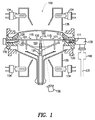
[0027]ある適切なデバイス、一度に1つのウェーハが処理チャンバで処理されるシングルウェーハプロセッサが図1に示されている。サセプタ120はチャンバ100を、サセプタの下方にある部分(下部)124と、サセプタの上方にある第2の部分(上部)122とに分割する。サセプタ120は概して、これを中心としてサセプタを回転させるシャフト126に搭載されており、より均一なウェーハの処理を達成する。堆積ガス115などの処理ガスの流れがチャンバの上部122に提供される。チャンバは概して、この一方の側にガス入口通路178を、反対側にガス排出通路113を有しており、ウェーハ全体にわたる処理ガスの流れを達成する。サセプタ120は、所望の処理温度にウェーハを加熱するために加熱される。特定の実施形態によると、サセプタを加熱するために使用される方法の1つは、チャンバ周辺に提供されたランプ134を使用して、チャンバ内およびサセプタ120上に光を向けることによるものである。ウェーハが加熱される温度をコントロールするために、サセプタの温度は常に測定される。これはしばしば、加熱されたサセプタから放射された赤外線を検出する赤外線温度センサー136によって達成される。反射器135はまた、チャンバに光を反射するために提供されてもよい。
[0027] One suitable device, a single wafer processor, in which one wafer at a time is processed in a processing chamber, is shown in FIG. The
[0028]水素などの不活性ガス121の流れが、サセプタの後部表面への材料の堆積を防止するために、チャンバの上部における堆積ガスよりもわずかに高い圧力でチャンバの下部に提供されてもよい。これを達成するための装置の1つが、“Gas Inlets For Wafer Processing Chamber”と題された、Roger N.Andersonらの米国特許第5,916,369号の出願に説明されている。チャンバの下部の不活性ガスは高圧であるため、これはチャンバの下部からチャンバの上部へとサセプタの縁部周辺を流れることになる。不活性ガスのこの流れは、チャンバの下部への堆積ガス115の流れを防止する。 [0028] A flow of an inert gas 121 such as hydrogen may be provided at the bottom of the chamber at a slightly higher pressure than the deposition gas at the top of the chamber to prevent material deposition on the back surface of the susceptor. Good. One apparatus for accomplishing this is Roger N., entitled “Gas Inlets For Wafer Processing Chamber”. Described in Anderson et al., US Pat. No. 5,916,369. Since the inert gas at the bottom of the chamber is at high pressure, it will flow around the edge of the susceptor from the bottom of the chamber to the top of the chamber. This flow of inert gas prevents the flow of deposition gas 115 to the bottom of the chamber.
[0029]上記反応器に関する説明は主に例示目的であり、本発明は、電子サイクロトロン共鳴(ECR)プラズマCVDデバイス、誘導結合RF高密度プラズマCVDデバイスなどの他のCVD機器と併用されてもよい。本発明はまた、熱CVDデバイス、プラズマエッチングデバイスおよび物理気相堆積デバイスと併用されてもよい。排出ライン内の堆積集積を防止するための本発明の装置および方法は具体的な半導体処理装置、あるいは具体的な堆積またはエッチングプロセスまたは方法に制限されない。 [0029] The above reactor description is primarily for illustrative purposes, and the present invention may be used in conjunction with other CVD equipment such as electron cyclotron resonance (ECR) plasma CVD devices, inductively coupled RF high density plasma CVD devices, etc. . The present invention may also be used with thermal CVD devices, plasma etching devices and physical vapor deposition devices. The apparatus and method of the present invention for preventing deposition accumulation in an exhaust line is not limited to a specific semiconductor processing apparatus, or a specific deposition or etching process or method.
[0030]CVD反応器100によって実施される化学気相堆積プロセスなどの半導体処理動作時に、多様なガス状廃棄生成物および汚染物がチャンバ100から排出ライン131に排出される。上記のように、堆積ガス115が排出通路113を介してチャンバを出ると、堆積ガスは冷却および凝縮して、排出通路113内に排出生成物111を形成する。これらの排出生成物111はまた排出キャップ130および排出ライン131に堆積される。実行中の特定の動作に応じて、これらの排出生成物111は、ポリマー材料と、排出ラインを介して排出される際に排出ライン131内に残渣や類似の粉末材料を残す部分反応生成物および副生成物などの微粒子物質とを含んでもよい。例えば、前駆体としてシラン(SiH4)、窒素(N2)およびアンモニア(NH3)を使用して窒化シリコン膜を堆積する際に、Six、Ny、Hz、Six、Hy、SiOxおよび元素シリコンからなる茶色粉末の形態の残渣が排出ラインに観察された。この残渣集積は、SiH4+N2+NH3の反応の半反応副生成物によるものと考えられる。同様の残渣はまた、ジシラン(Si2H6)や有機ソースなどの他の前駆体ガスや液体を使用して窒化シリコン層を堆積する際に形成される。残渣集積はまた、他の層への酸窒化膜および酸化シリコン膜の堆積時に生じることがあり、またプラズマエッチングおよび他のプロセスステップ時に生じることもある。空気に曝露されなかった粘性材料は、空気に曝露されていない時にはクロロシランポリマーからなることが観察された。これらのポリマーは水と反応してシロキサンポリマーを形成する。空気に曝露されると、この粘性液体は固体残渣に凝縮し、この例は上述されている。
[0030] During a semiconductor processing operation, such as a chemical vapor deposition process performed by the
[0031]本発明の実施形態は、真空排出ラインを介して排出された反応ガスにおける成分の付着物を破壊および/または防止し、かつこのポリマー化を防止することによって、このような残渣および微粒子物質の集積を防止する。本発明の実施形態は、排出ラインの洗浄を支援するために、低圧プラズマと共に利用可能である。 [0031] Embodiments of the present invention provide such residues and particulates by destroying and / or preventing component deposits in the reaction gas exhausted through the vacuum exhaust line and preventing this polymerization. Prevent material accumulation. Embodiments of the present invention can be used with a low pressure plasma to assist in cleaning the exhaust line.
[0032]引き続き図1を参照すると、CVD反応器100は、本発明の1つ以上の実施形態に従った付着物破壊または付着物防止装置140が嵌合されている。排出ラインにポリマーを形成する種のポリマー化を低減および/または防止する付着物破壊または付着物防止装置140は、排出ガス源である処理チャンバ100の下流に位置決めされている。装置140は、排出ライン131の一部に接続するか、これを置換することができる。
[0032] With continued reference to FIG. 1, the
[0033]図1において、排出ライン131におけるポリマーの形成を破壊または防止するための付着物破壊または付着物防止装置140(以下「ポリマー防止装置」と称する)は、排出ライン131の一部に沿って、真空ポンプシステムと真空マニホルド間に嵌合される。この位置ゆえに、真空チャンバ100から排出されたガスは必ずポリマー防止装置140を通過する。ポリマー防止装置140は排出ライン131に沿った任意の場所に位置決めされてもよいが、好ましくは、ポリマー防止装置140は可能な限り排出キャップ130の近くに位置決めされるため、チャンバ100から排出されたガスは、排出ライン131の任意の部分を通過する前にポリマー防止装置140を通過する。
In FIG. 1, a deposit destruction or deposit prevention device 140 (hereinafter referred to as a “polymer prevention device”) for breaking or preventing polymer formation in the
[0034]動作時に、堆積ガスが排出ライン131を介して真空チャンバから排出されると、ポリマー防止装置140は、排出ラインにおけるポリマー種の形成を許容する付着物を破壊または付着物形成を防止するように動作することによって、排出ライン131におけるこのようなポリマー種の形成を防止することができる。ポリマー形成を防止するために、ポリマー防止装置140は堆積動作および洗浄動作両方においてONにされてもよく、あるいは洗浄手順時のみ活性化されてもよい。
[0034] In operation, when deposition gas is exhausted from the vacuum chamber via the
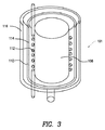
[0035]ポリマー防止装置の具体的な実施形態について次に説明する。図2から図5をまず参照すると、ポリマー防止装置は、排出キャップ130に取り付けられている下流高温チャンバ101を含んでもよい。示されている実施形態では、下流高温チャンバ101は低周波数RFチャンバであってもよい。ここで使用されているように、低周波数とは、約20KHz未満のRF周波数を意味しており、通常は約10KHz未満である。RFチャンバは、排出ラインにポリマーを形成する付着物を破壊または防止するのに十分な温度を生成可能である。ポリマーを形成する付着物を破壊または防止するのに十分な温度は約1000℃を超え、通常は1050℃を超え、さらに一般的には約1100℃〜約1200℃の範囲にある。
[0035] Specific embodiments of the polymer prevention device will now be described. Referring first to FIGS. 2-5, the polymer prevention device may include a downstream
[0036]高温チャンバ101のコンポーネントは、SiCや他の適切な材料から作られてもよい上部バッフル102および底部バッフル104を含んでおり、これらは第1のクリア石英ライナー108によって囲まれているグラファイトサセプタチューブ106を挟持およびサポートしており、これについては図3および4に示されている。図3および5を参照すると、第2の不透明石英ライナー110はクリア石英ライナー108を囲んでいる。適切なコイル112、例えば、低周波数RFエネルギーを生成するニッケルめっき銅コイルが、不透明石英ライナー110を囲んでいる。セラミックライナー114はコイル112を囲んでおり、このセラミックライナーはステンレス鋼ライナー116によって囲まれている。このステンレス鋼ライナー116は少なくとも2つの目的を果たす。第1に、これはCVD処理装置100および他の機器を、コイルによって生成された電圧および雑音信号からシールドする。第2に、セラミックライナー114が破壊またはひび割れする場合、あるいは真空シールチャンバ101が別の態様で破壊される場合、ライナー116は、排出ガスが逃げるのを防止する第2のシールを提供する。ライナー116は、アルミニウムや鋼などの多様な金属または他の化合物から作られることが可能であり、好ましくはシールド効果のために接地されている。図5に示されているように、不透明石英放射バッフル118は、熱分離を提供するために、下流高温チャンバ101の出口部分に提供されてもよい。
[0036] The components of the
[0037]上記提供された下流高温チャンバ101の詳細は例示的な実施形態にすぎず、またこの設計の変形例が利用可能である点が当然理解されるであろう。排出ラインにおいてポリマーを形成する付着物を破壊または防止するのに十分な温度を生成するための低周波数RFチャンバの動作についての詳細は、実験的に判断可能である。約1000℃〜1200℃の温度を達成可能な高温RFチャンバが当技術分野において既知である。
[0037] It will be appreciated that the details of the downstream
[0038]プラズマを形成するために下流高温チャンバ101内に作成された電圧場は、容量結合電極、誘導結合コイルまたはECR技術などの多様な既知の方法を使用して生成可能である。しかしながら、コンパクトなサイズ、および比較的高い電圧場を作成する容量ゆえに、ヘリカル共鳴コイルなどの誘導コイルによって電圧場を作成することが好ましい。このようなコイルは当業者には既知であり、参照してここに組み込まれているMichael A.LiebermanおよびAllan J.Lichtenbergによる“Principles of Plasma Discharges and Materials Processing”、pp404−410、John Wiley&Sons(1994)などの多数の既知のテキストのいずれかに説明されている基準に従って設計されてもよい。
[0038] The voltage field created in the downstream
[0039]ヘリカル共鳴コイルは、銅、ニッケルまたは金などの高導電タイプ金属あるいは類似の導電材料から作られることが可能である。このコイルを適切に共鳴させるためには、コイルの長さは、印加されたRF信号の波長のほぼ1/4か、これよりわずかに長いことが重要である。この長さのコイルは、高温チャンバ101における種の分解をさらに高めるより強力かつより強烈な電圧場を作成する。
[0039] The helical resonance coil can be made of a highly conductive type metal such as copper, nickel or gold or similar conductive material. In order for this coil to resonate properly, it is important that the length of the coil be approximately ¼ or slightly longer than the wavelength of the applied RF signal. This length of coil creates a stronger and more intense voltage field that further enhances seed decomposition in the
[0040]ヘリカル共鳴コイルは、一方の端部ではRF電源に、反対側の端部では接地電位に接続されている。下流高温チャンバ101を通過し、および/またはこの中に堆積される材料の完全な反応を保証するために、高温チャンバ101は、グラファイトチューブを約1000℃を超える温度に加熱し、かつ低周波数プラズマを任意に形成するのに十分なレベルでRF電源によって駆動されなければならない。概して、50〜1000ワット以上の電力レベルが用いられることが可能であり、好ましくは100〜400ワットの電力レベルが使用される。実際に選択された電力レベルは、低周波数プラズマを形成するのに十分な電力レベルを使用するという要望と、低電力レベルを使用してエネルギーコストを節約して、より小型かつ安価な電源の使用を許容するという要望のバランスをとることによって判断されるべきである。
[0040] The helical resonance coil is connected to an RF power source at one end and to a ground potential at the opposite end. In order to ensure complete reaction of the material that passes through and / or deposited in the downstream
[0041]高温チャンバ101を駆動する電源は約10KHz未満の周波数範囲で操作される。この周波数範囲では、排出ラインの洗浄さらに助長するために、高イオン衝突が提供される。
[0041] The power supply driving the
[0042]RF電源は、単一周波数RFソースまたは混合周波数RFソースのいずれかから供給可能である。電源の電力出力は、下流高温チャンバ101が使用される用途と、下流高温チャンバ101で処置されるガスの容積とに左右される。RF電力は、反応チャンバ100に電源投入するのに使用されるRF電源から導出可能であり、あるいはポリマー防止装置140のみを駆動する個別RF電源103によって供給可能である。加えて、複数の処理チャンバが洗浄ルームにあるとすると、反応チャンバ100に接続されている複数の下流高温チャンバ101がすべて、適切な数のRF電力スプリッターに接続されている個別の専用RF電源によって駆動されてもよい。
[0042] The RF power source can be supplied from either a single frequency RF source or a mixed frequency RF source. The power output of the power supply depends on the application in which the downstream
[0043]下流高温チャンバ101の長さおよびサイズは変更可能である。一部の用途では、高温チャンバの長さはわずか4〜6インチまたはこれより短くてもよいが、他の用途では、下流高温チャンバ101は排出ライン131の全長(4〜5フィート以上)であってもよいため、このラインを置換することができる。コイルの長さはRF波長の1/4よりわずかに長いはずであるため、使用されているコイル長とRF周波数間には直接の関係がある。より長いコイルはより低い周波数RF電力信号を必要とする。
[0043] The length and size of the downstream
[0044]上記下流高温チャンバ101は、排出ラインを洗浄するために熱モードでのみ利用可能であり、あるいは、低周波数RFチャンバで生成可能な低圧プラズマと共に使用されてもよい。ここで使用されているように、低圧とは約20トール未満の圧力のことであり、通常は約10トール未満である。加えて、HCl、NF3、Cl2およびF2などの種々のエッチャント種が、洗浄プロセスを補強するために活性化可能である。エッチャント種は、排出キャップ130と連通している入口ポート98に導入可能である。
[0044] The downstream
[0045]ウェーハ処理チャンバからの堆積後の堆積物を洗浄するための塩素含有ガスの使用は、米国特許第6,042,654号に説明されており、この内容全体は参照してここに組み込まれている。米国特許第6,042,654号に説明されている方法では、塩素ガスを加熱することによって塩素ラジカルが形成され、塩素ラジカルが処理チャンバにおける堆積物と反応される。 [0045] The use of a chlorine-containing gas to clean post-deposition deposits from a wafer processing chamber is described in US Pat. No. 6,042,654, the entire contents of which are incorporated herein by reference. It is. In the method described in US Pat. No. 6,042,654, chlorine radicals are formed by heating chlorine gas and the chlorine radicals are reacted with deposits in the processing chamber.
[0046]高温洗浄プロセスおよび装置の利点は、HClが高温で洗浄ガスとして使用可能である点である。一実施形態では、HClがエッチャント種として使用される場合、下流高温チャンバ101は約1200℃にまで加熱される。高温チャンバ101がHClガスの解離温度を超える1200℃に達すると、HClは下流高温チャンバ101に導入される。高温の結果として、HClは反応性水素(H)および塩素(Cl)に解離し、これらはシリコン副生成物と反応することになる。エッチャントとしてHClを利用する実施形態では、下流RFチャンバは、約1150℃より高いHClの解離温度を超えて加熱されるはずである。この温度未満では、HClはポリマーを破壊しないと考えられている。
[0046] An advantage of the high temperature cleaning process and apparatus is that HCl can be used as a cleaning gas at high temperatures. In one embodiment, downstream
[0047]したがって、1つ以上の実施形態によると、ポリマー排出堆積物の形成は、ポリマー排出成分を形成する付着物を破壊したり、このような付着物の形成を防止したりするのに十分な温度に低周波数RFチャンバを加熱することによって防止される。加えて、加熱は、下流RFチャンバにおいてエッチャント種を活性化させるために使用可能である。約1000℃を超え、より一般的には約1100℃を超え、例えば約1100℃〜1200℃の温度が、付着物を破壊して排出成分のポリマー化を防止するために使用可能であり、またエッチャント種を活性化させるために使用可能である。 [0047] Thus, according to one or more embodiments, the formation of polymer discharge deposits is sufficient to destroy deposits that form polymer discharge components or to prevent the formation of such deposits. This is prevented by heating the low frequency RF chamber to a certain temperature. In addition, heating can be used to activate the etchant species in the downstream RF chamber. A temperature above about 1000 ° C., more typically above about 1100 ° C., for example about 1100 ° C. to 1200 ° C., can be used to destroy deposits and prevent polymerisation of the exhaust components, and Can be used to activate etchant species.
[0048]ポリマー防止装置140が処理手順の具体的期間にONおよびOFFにされてもよい点は既に説明されているが、このポリマー防止装置はまたパッシブデバイスとして構成されてもよい。パッシブデバイスとして、ポリマー防止装置140が上記下流高温チャンバ101である場合、高温チャンバ101は十分なRF電力信号を継続的に供給されるため、高温チャンバ101をONおよびOFFにするために特殊なコントロール信号やプロセッサ時間が費やされる必要はない。
[0048] Although it has already been described that the
[0049]上述のように、アクティブデバイスとして構成される場合、電力は、チャンバ洗浄動作が生じる期間にポリマー防止装置140に供給される。任意に、RF電力はまた、膜堆積がチャンバ100に生じる期間に供給されてもよい。アクティブデバイスとして構成される場合のポリマー防止装置140のタイミング態様のコントロールは概して、コントロールラインで送信されたコントロール信号の適用によってプロセッサ(図示せず)で実行される。
[0049] As described above, when configured as an active device, power is supplied to the
[0050]本発明の装置の多数の代替実施形態が構築可能である。上記図1に示されているポリマー防止装置140は、排出キャップに結合されている真空UVデバイスの形態であってもよい。このような装置の例示的実施形態が図6に示されている。図7において、UVデバイス200は、反応チャンバ100の排出キャップ130に結合されて、排出ライン131の上流にある。UVデバイス200は、排出キャップに結合されるのに加えて、またはこれに代わって排出ライン131に結合されてもよい点が認識されるであろう。入口ラインは、HCl、NF3、Cl2およびF2などのエッチャント種を添加するために排出キャップ130または排出ラインに結合されてもよい。エッチャント種は、洗浄動作を補強するために、排出ラインや排出キャップに注入可能である。
[0050] Numerous alternative embodiments of the apparatus of the present invention can be constructed. The
[0051]図7は、図7に示されている実施形態で利用可能なUVデバイス200の実施形態を示している。図7において、UVデバイスは、Osram Sylvania of Danvers,MAから市販されているXeradex(登録商標)電球を含む。代替的に、UV源は、USHIO America,Incによって供給されたランプであってもよい。電球の波長は、使用されているエッチャントのタイプに左右されることになる。適切な波長は、Cl2がエッチャントガスである場合172nmおよび124nmを含む。電球202は、UVウィンドウ204で排出キャップに取り付けられてもよく、これは通常、Oリングなどの適切なシール206、208でシールされている。ランプエンクロージャ210は、窒素や他のガス用のパージバルブ212を含んでもよい。
[0051] FIG. 7 illustrates an embodiment of a
[0052]使用時に、電球202によって生成されたUVエネルギーは付着物の形成を防止したり、排出ラインにポリマー種を形成するのに必要な付着物を破壊したりする。揮発種はガス相に残っており、またガス相における排出ライン131を介してポンピングされる。HClがエッチャントとして使用される場合、これはUV光では反応性が高く、また洗浄プロセスを補強すると考えられる。排出ラインをUVデバイス200の下流に少なくとも約3〜4フィート加熱することによって洗浄プロセスをさらに高めることが望ましいであろう。
[0052] In use, the UV energy generated by the
[0053]ここで本発明は特定の実施形態を参照して説明されてきたが、これらの実施形態は本発明の原理および用途の例示にすぎない点が理解されるはずである。本発明の主旨および範囲から逸脱することなく本発明の方法に対する種々の修正および変形が可能である点は当業者に明らかである。したがって、本発明は、添付の請求項および同等物の範囲内の修正および変形を含むことが意図されている。 [0053] Although the invention herein has been described with reference to particular embodiments, it is to be understood that these embodiments are merely illustrative of the principles and applications of the present invention. It will be apparent to those skilled in the art that various modifications and variations can be made to the method of the present invention without departing from the spirit and scope of the invention. Thus, it is intended that the present invention include modifications and variations that are within the scope of the appended claims and their equivalents.
100…CVD反応器、101…下流高温チャンバ、102…上部バッフル、103…RF電源、104…底部バッフル、106…サセプタチューブ、108…クリア石英ライナー、110…不透明石英ライナー、111…排出生成物、112…コイル、113…ガス排出通路、114…セラミックライナー、115…堆積ガス、116…ステンレス鋼ライナー、118…放射バッフル、120…サセプタ、121…不活性ガス、122…上部、124…下部、126…シャフト、130…排出キャップ、131…排出ライン、134…ランプ、135…反射器、140…ポリマー防止装置、178…ガス入口通路、200…UVデバイス、202…電球、204…UVウィンドウ、206、208…シール、210…ランプエンクロージャ、212…パージバルブ
DESCRIPTION OF
Claims (14)
前記CVD反応チャンバは、基板サポートと、反応チャンバに塩素含有ガスを導入するガス分布システムとを含み、
クロロシランポリマーを形成する付着物を破壊し、および/または付着物を防止して、
前記排出ラインにおけるクロロシランポリマーの形成を防止するに足る温度を生成、維持する誘導性の低周波数RFチャンバを含む下流チャンバを介して、前記CVD反応チャンバから塩素含有ガスおよび塩素含有副産物を除くステップを備え、
前記低周波数RFチャンバは20KHz未満の周波数で動作する、
方法。 A method for preventing the formation of chlorosilane polymer in a discharge line of a CVD reaction chamber, comprising:
The CVD reaction chamber includes a substrate support and a gas distribution system that introduces a chlorine-containing gas into the reaction chamber;
Destroying and / or preventing deposits forming chlorosilane polymers;
Generating a temperature sufficient to prevent the formation of chlorosilane polymers in the exhaust line, through the downstream chamber includes a low frequency RF chamber inductive maintaining, the steps except the chlorine-containing gas and chlorine-containing by-products from the CVD reaction chamber Prepared ,
The low frequency RF chamber operates at a frequency of less than 20 KHz;
Method.
CVD反応チャンバから塩素含有ガスおよび塩素含有副産物を除去するための、前記反応チャンバに接続されている排出ラインと、
前記排出ラインにおけるクロロシランポリマーの形成を防止するための、前記排出ラインに結合されているデバイスであって、誘導性の低周波数RFチャンバを含み、クロロシランポリマーの形成を防止するに足る温度を生成、維持するデバイスと、
を備え、
前記低周波数RFチャンバは20KHz未満の周波数で動作する、
CVD装置。 A CVD reaction chamber that includes a substrate support and a gas distribution system that introduces a chlorine-containing gas into the reaction chamber;
An exhaust line connected to the reaction chamber for removing chlorine-containing gases and chlorine-containing by-products from the CVD reaction chamber;
A device coupled to the exhaust line for preventing the formation of chlorosilane polymer in the exhaust line, including an inductive low frequency RF chamber, generating a temperature sufficient to prevent the formation of the chlorosilane polymer; A device to maintain,
Equipped with a,
The low frequency RF chamber operates at a frequency of less than 20 KHz;
CVD equipment.
Applications Claiming Priority (3)
| Application Number | Priority Date | Filing Date | Title |
|---|---|---|---|
| US11/435,065 | 2006-05-16 | ||
| US11/435,065 US20070267143A1 (en) | 2006-05-16 | 2006-05-16 | In situ cleaning of CVD system exhaust |
| PCT/US2007/068948 WO2007137035A2 (en) | 2006-05-16 | 2007-05-15 | In situ cleaning of cvd system exhaust |
Publications (3)
| Publication Number | Publication Date |
|---|---|
| JP2009537993A JP2009537993A (en) | 2009-10-29 |
| JP2009537993A5 JP2009537993A5 (en) | 2010-05-20 |
| JP5269770B2 true JP5269770B2 (en) | 2013-08-21 |
Family
ID=38659696
Family Applications (1)
| Application Number | Title | Priority Date | Filing Date |
|---|---|---|---|
| JP2009511203A Expired - Fee Related JP5269770B2 (en) | 2006-05-16 | 2007-05-15 | In-situ cleaning of CVD system discharge |
Country Status (7)
| Country | Link |
|---|---|
| US (2) | US20070267143A1 (en) |
| JP (1) | JP5269770B2 (en) |
| KR (1) | KR101046969B1 (en) |
| CN (1) | CN101535525B (en) |
| DE (1) | DE112007001223T5 (en) |
| TW (1) | TWI388689B (en) |
| WO (1) | WO2007137035A2 (en) |
Families Citing this family (19)
| Publication number | Priority date | Publication date | Assignee | Title |
|---|---|---|---|---|
| DE102009043848A1 (en) * | 2009-08-25 | 2011-03-03 | Aixtron Ag | CVD method and CVD reactor |
| KR101590661B1 (en) * | 2010-09-13 | 2016-02-01 | 도쿄엘렉트론가부시키가이샤 | Liquid processing apparatus, liquid processing method and storage medium |
| JP5926742B2 (en) | 2010-12-30 | 2016-05-25 | ビーコ・インストゥルメンツ・インコーポレイテッド | Reactor and method for processing wafers |
| KR101884003B1 (en) * | 2011-03-22 | 2018-07-31 | 어플라이드 머티어리얼스, 인코포레이티드 | Liner assembly for chemical vapor deposition chamber |
| CN102615068B (en) * | 2012-03-26 | 2015-05-20 | 中微半导体设备(上海)有限公司 | Cleaning method for MOCVD equipment |
| CN104246983B (en) * | 2012-04-24 | 2017-03-29 | 应用材料公司 | The gas of high power capacity epitaxial silicon deposition system is reclaimed and abatement system |
| US9388493B2 (en) | 2013-01-08 | 2016-07-12 | Veeco Instruments Inc. | Self-cleaning shutter for CVD reactor |
| SG11201508512PA (en) * | 2013-05-23 | 2015-12-30 | Applied Materials Inc | A coated liner assembly for a semiconductor processing chamber |
| JP5605464B2 (en) * | 2013-06-25 | 2014-10-15 | 東京エレクトロン株式会社 | Film forming apparatus and cleaning method thereof |
| US11414759B2 (en) * | 2013-11-29 | 2022-08-16 | Taiwan Semiconductor Manufacturing Co., Ltd | Mechanisms for supplying process gas into wafer process apparatus |
| CN103938177B (en) * | 2014-05-07 | 2015-12-30 | 南昌黄绿照明有限公司 | The non brazing MOCVD shower nozzle of available chlorine on-line cleaning |
| KR102372893B1 (en) | 2014-12-04 | 2022-03-10 | 삼성전자주식회사 | Chemical vapor deposition apparatus for fabricating light emitting diode(LED) |
| JP6625891B2 (en) | 2016-02-10 | 2019-12-25 | 株式会社日立ハイテクノロジーズ | Vacuum processing equipment |
| TWI609988B (en) * | 2016-07-21 | 2018-01-01 | 台灣積體電路製造股份有限公司 | Process equipment and chemical vapor deposition process |
| US11332824B2 (en) * | 2016-09-13 | 2022-05-17 | Lam Research Corporation | Systems and methods for reducing effluent build-up in a pumping exhaust system |
| JP7080140B2 (en) * | 2018-09-06 | 2022-06-03 | 東京エレクトロン株式会社 | Board processing equipment |
| CN111069192A (en) * | 2018-10-22 | 2020-04-28 | 北京北方华创微电子装备有限公司 | In-situ cleaning device and semiconductor processing equipment |
| KR102368157B1 (en) | 2020-02-03 | 2022-03-02 | 주식회사 제이엔케이 | Apparatus for low pressure chemical vapor deposition |
| KR102421233B1 (en) | 2020-02-03 | 2022-07-18 | 주식회사 제이엔케이 | Apparatus for low pressure chemical vapor deposition |
Family Cites Families (40)
| Publication number | Priority date | Publication date | Assignee | Title |
|---|---|---|---|---|
| US4263873A (en) * | 1979-03-19 | 1981-04-28 | George Christianson | Animal litter and method of preparation |
| US4263872A (en) * | 1980-01-31 | 1981-04-28 | Rca Corporation | Radiation heated reactor for chemical vapor deposition on substrates |
| JPS60114570A (en) * | 1983-11-25 | 1985-06-21 | Canon Inc | Evacuating system for plasma cvd device |
| US4960488A (en) * | 1986-12-19 | 1990-10-02 | Applied Materials, Inc. | Reactor chamber self-cleaning process |
| US5158644A (en) * | 1986-12-19 | 1992-10-27 | Applied Materials, Inc. | Reactor chamber self-cleaning process |
| US5451378A (en) * | 1991-02-21 | 1995-09-19 | The United States Of America As Represented By The Secretary Of The Navy | Photon controlled decomposition of nonhydrolyzable ambients |
| FR2686347B1 (en) * | 1992-01-22 | 1994-10-07 | Lorraine Carbone | METHOD OF PYROLYSIS OF FLUID EFFLUENTS AND CORRESPONDING DEVICE. |
| US5916369A (en) | 1995-06-07 | 1999-06-29 | Applied Materials, Inc. | Gas inlets for wafer processing chamber |
| US5454903A (en) * | 1993-10-29 | 1995-10-03 | Applied Materials, Inc. | Plasma cleaning of a CVD or etch reactor using helium for plasma stabilization |
| RU95106478A (en) * | 1994-04-29 | 1997-01-20 | Моторола | Arrangement and method for degradation of chemical compounds |
| US5855677A (en) * | 1994-09-30 | 1999-01-05 | Applied Materials, Inc. | Method and apparatus for controlling the temperature of reaction chamber walls |
| US5811022A (en) * | 1994-11-15 | 1998-09-22 | Mattson Technology, Inc. | Inductive plasma reactor |
| US6194628B1 (en) * | 1995-09-25 | 2001-02-27 | Applied Materials, Inc. | Method and apparatus for cleaning a vacuum line in a CVD system |
| US6187072B1 (en) * | 1995-09-25 | 2001-02-13 | Applied Materials, Inc. | Method and apparatus for reducing perfluorocompound gases from substrate processing equipment emissions |
| US6045618A (en) * | 1995-09-25 | 2000-04-04 | Applied Materials, Inc. | Microwave apparatus for in-situ vacuum line cleaning for substrate processing equipment |
| US5963833A (en) * | 1996-07-03 | 1999-10-05 | Micron Technology, Inc. | Method for cleaning semiconductor wafers and |
| US5788778A (en) * | 1996-09-16 | 1998-08-04 | Applied Komatsu Technology, Inc. | Deposition chamber cleaning technique using a high power remote excitation source |
| US5827370A (en) * | 1997-01-13 | 1998-10-27 | Mks Instruments, Inc. | Method and apparatus for reducing build-up of material on inner surface of tube downstream from a reaction furnace |
| US5743581A (en) * | 1997-03-18 | 1998-04-28 | Applied Materials Incorporated | Semiconductor process chamber exhaust port quartz removal tool |
| US6153260A (en) * | 1997-04-11 | 2000-11-28 | Applied Materials, Inc. | Method for heating exhaust gas in a substrate reactor |
| US6815633B1 (en) * | 1997-06-26 | 2004-11-09 | Applied Science & Technology, Inc. | Inductively-coupled toroidal plasma source |
| JP3500050B2 (en) * | 1997-09-08 | 2004-02-23 | 東京エレクトロン株式会社 | Impurity removing device, film forming method and film forming system |
| US6042654A (en) * | 1998-01-13 | 2000-03-28 | Applied Materials, Inc. | Method of cleaning CVD cold-wall chamber and exhaust lines |
| US6098637A (en) * | 1998-03-03 | 2000-08-08 | Applied Materials, Inc. | In situ cleaning of the surface inside a vacuum processing chamber |
| US20030164225A1 (en) * | 1998-04-20 | 2003-09-04 | Tadashi Sawayama | Processing apparatus, exhaust processing process and plasma processing |
| US6368567B2 (en) * | 1998-10-07 | 2002-04-09 | Applied Materials, Inc. | Point-of-use exhaust by-product reactor |
| JP3709432B2 (en) * | 1999-04-30 | 2005-10-26 | アプライド マテリアルズ インコーポレイテッド | Exhaust gas treatment device and substrate treatment device |
| KR100613674B1 (en) * | 1999-05-14 | 2006-08-21 | 동경 엘렉트론 주식회사 | Method and apparatus for processing wafer |
| US6255222B1 (en) * | 1999-08-24 | 2001-07-03 | Applied Materials, Inc. | Method for removing residue from substrate processing chamber exhaust line for silicon-oxygen-carbon deposition process |
| US6572924B1 (en) * | 1999-11-18 | 2003-06-03 | Asm America, Inc. | Exhaust system for vapor deposition reactor and method of using the same |
| US6596123B1 (en) * | 2000-01-28 | 2003-07-22 | Applied Materials, Inc. | Method and apparatus for cleaning a semiconductor wafer processing system |
| US7378062B2 (en) * | 2000-05-29 | 2008-05-27 | Three Tec Co., Ltd. | Object processing apparatus and plasma facility comprising the same |
| WO2002000962A1 (en) * | 2000-06-28 | 2002-01-03 | Mks Instruments, Inc. | System and method for in-situ cleaning of process monitor of semi-conductor wafer fabricator |
| US6843258B2 (en) * | 2000-12-19 | 2005-01-18 | Applied Materials, Inc. | On-site cleaning gas generation for process chamber cleaning |
| US7084832B2 (en) * | 2001-10-09 | 2006-08-01 | Plasma Control Systems, Llc | Plasma production device and method and RF driver circuit with adjustable duty cycle |
| US6902629B2 (en) * | 2002-04-12 | 2005-06-07 | Applied Materials, Inc. | Method for cleaning a process chamber |
| US6923189B2 (en) * | 2003-01-16 | 2005-08-02 | Applied Materials, Inc. | Cleaning of CVD chambers using remote source with cxfyoz based chemistry |
| KR100505670B1 (en) * | 2003-02-05 | 2005-08-03 | 삼성전자주식회사 | Apparatus for manufacturing semiconductor device having hot fluid supplier for removing byproducts |
| US6872909B2 (en) * | 2003-04-16 | 2005-03-29 | Applied Science And Technology, Inc. | Toroidal low-field reactive gas and plasma source having a dielectric vacuum vessel |
| US7969096B2 (en) * | 2006-12-15 | 2011-06-28 | Mks Instruments, Inc. | Inductively-coupled plasma source |
-
2006
- 2006-05-16 US US11/435,065 patent/US20070267143A1/en not_active Abandoned
-
2007
- 2007-05-10 TW TW096116708A patent/TWI388689B/en not_active IP Right Cessation
- 2007-05-15 KR KR1020087030343A patent/KR101046969B1/en not_active IP Right Cessation
- 2007-05-15 WO PCT/US2007/068948 patent/WO2007137035A2/en active Application Filing
- 2007-05-15 JP JP2009511203A patent/JP5269770B2/en not_active Expired - Fee Related
- 2007-05-15 DE DE112007001223T patent/DE112007001223T5/en not_active Withdrawn
- 2007-05-15 CN CN2007800159887A patent/CN101535525B/en not_active Expired - Fee Related
-
2008
- 2008-10-02 US US12/244,318 patent/US8343317B2/en not_active Expired - Fee Related
Also Published As
| Publication number | Publication date |
|---|---|
| US20070267143A1 (en) | 2007-11-22 |
| TW200804619A (en) | 2008-01-16 |
| KR101046969B1 (en) | 2011-07-06 |
| CN101535525B (en) | 2012-12-19 |
| US8343317B2 (en) | 2013-01-01 |
| DE112007001223T5 (en) | 2009-04-23 |
| WO2007137035A2 (en) | 2007-11-29 |
| WO2007137035A3 (en) | 2008-12-11 |
| TWI388689B (en) | 2013-03-11 |
| KR20090016476A (en) | 2009-02-13 |
| CN101535525A (en) | 2009-09-16 |
| US20090044699A1 (en) | 2009-02-19 |
| JP2009537993A (en) | 2009-10-29 |
Similar Documents
| Publication | Publication Date | Title |
|---|---|---|
| JP5269770B2 (en) | In-situ cleaning of CVD system discharge | |
| EP0839929B1 (en) | Method and apparatus for minimizing deposition in an exhaust line | |
| JP3897382B2 (en) | Vacuum system cleaning method and apparatus for CVD system | |
| KR100495783B1 (en) | Parallel plate apparatus for in-situ vacuum line cleaning for substrate processing equipment | |
| KR100767762B1 (en) | A CVD semiconductor-processing device provided with a remote plasma source for self cleaning | |
| KR100271694B1 (en) | Method and apparatus for reducing perfluorocompound gases from substrate processing equipment emission | |
| KR100696030B1 (en) | Improved method for removing residue from substrate processing chamber exhaust line for silicon-oxygen-carbon deposition process | |
| JP4916119B2 (en) | Equipment for reducing white powder during silicon nitride deposition using remote plasma source cleaning technology | |
| JP2006121073A (en) | End point detector and particle monitor | |
| JPH1171680A (en) | Device for improved remote microwave plasma source used together with substrate treating apparatus | |
| JPH1174258A (en) | Method and device for obtaining final point in plasma cleaning process | |
| US6564810B1 (en) | Cleaning of semiconductor processing chambers | |
| TW536739B (en) | Apparatus for exhaust white powder elimination in substrate processing | |
| US20080124670A1 (en) | Inductively heated trap |
Legal Events
| Date | Code | Title | Description |
|---|---|---|---|
| A521 | Request for written amendment filed |
Free format text: JAPANESE INTERMEDIATE CODE: A523 Effective date: 20100331 |
|
| A621 | Written request for application examination |
Free format text: JAPANESE INTERMEDIATE CODE: A621 Effective date: 20100331 |
|
| A977 | Report on retrieval |
Free format text: JAPANESE INTERMEDIATE CODE: A971007 Effective date: 20101007 |
|
| RD03 | Notification of appointment of power of attorney |
Free format text: JAPANESE INTERMEDIATE CODE: A7423 Effective date: 20101130 |
|
| RD04 | Notification of resignation of power of attorney |
Free format text: JAPANESE INTERMEDIATE CODE: A7424 Effective date: 20101210 |
|
| A131 | Notification of reasons for refusal |
Free format text: JAPANESE INTERMEDIATE CODE: A131 Effective date: 20120508 |
|
| A521 | Request for written amendment filed |
Free format text: JAPANESE INTERMEDIATE CODE: A523 Effective date: 20120808 |
|
| RD04 | Notification of resignation of power of attorney |
Free format text: JAPANESE INTERMEDIATE CODE: A7424 Effective date: 20120925 |
|
| TRDD | Decision of grant or rejection written | ||
| A01 | Written decision to grant a patent or to grant a registration (utility model) |
Free format text: JAPANESE INTERMEDIATE CODE: A01 Effective date: 20130430 |
|
| A61 | First payment of annual fees (during grant procedure) |
Free format text: JAPANESE INTERMEDIATE CODE: A61 Effective date: 20130508 |
|
| R150 | Certificate of patent or registration of utility model |
Free format text: JAPANESE INTERMEDIATE CODE: R150 |
|
| R250 | Receipt of annual fees |
Free format text: JAPANESE INTERMEDIATE CODE: R250 |
|
| R250 | Receipt of annual fees |
Free format text: JAPANESE INTERMEDIATE CODE: R250 |
|
| LAPS | Cancellation because of no payment of annual fees |