JP7080140B2 - Board processing equipment - Google Patents
Board processing equipment Download PDFInfo
- Publication number
- JP7080140B2 JP7080140B2 JP2018166546A JP2018166546A JP7080140B2 JP 7080140 B2 JP7080140 B2 JP 7080140B2 JP 2018166546 A JP2018166546 A JP 2018166546A JP 2018166546 A JP2018166546 A JP 2018166546A JP 7080140 B2 JP7080140 B2 JP 7080140B2
- Authority
- JP
- Japan
- Prior art keywords
- gas
- chamber
- valve
- exhaust pipe
- exhaust
- Prior art date
- Legal status (The legal status is an assumption and is not a legal conclusion. Google has not performed a legal analysis and makes no representation as to the accuracy of the status listed.)
- Active
Links
Images


Classifications
-
- H—ELECTRICITY
- H01—ELECTRIC ELEMENTS
- H01J—ELECTRIC DISCHARGE TUBES OR DISCHARGE LAMPS
- H01J37/00—Discharge tubes with provision for introducing objects or material to be exposed to the discharge, e.g. for the purpose of examination or processing thereof
- H01J37/32—Gas-filled discharge tubes
- H01J37/32431—Constructional details of the reactor
- H01J37/32798—Further details of plasma apparatus not provided for in groups H01J37/3244 - H01J37/32788; special provisions for cleaning or maintenance of the apparatus
- H01J37/32816—Pressure
- H01J37/32834—Exhausting
- H01J37/32844—Treating effluent gases
-
- H—ELECTRICITY
- H01—ELECTRIC ELEMENTS
- H01L—SEMICONDUCTOR DEVICES NOT COVERED BY CLASS H10
- H01L21/00—Processes or apparatus adapted for the manufacture or treatment of semiconductor or solid state devices or of parts thereof
- H01L21/67—Apparatus specially adapted for handling semiconductor or electric solid state devices during manufacture or treatment thereof; Apparatus specially adapted for handling wafers during manufacture or treatment of semiconductor or electric solid state devices or components ; Apparatus not specifically provided for elsewhere
- H01L21/67005—Apparatus not specifically provided for elsewhere
- H01L21/67011—Apparatus for manufacture or treatment
- H01L21/67017—Apparatus for fluid treatment
-
- C—CHEMISTRY; METALLURGY
- C23—COATING METALLIC MATERIAL; COATING MATERIAL WITH METALLIC MATERIAL; CHEMICAL SURFACE TREATMENT; DIFFUSION TREATMENT OF METALLIC MATERIAL; COATING BY VACUUM EVAPORATION, BY SPUTTERING, BY ION IMPLANTATION OR BY CHEMICAL VAPOUR DEPOSITION, IN GENERAL; INHIBITING CORROSION OF METALLIC MATERIAL OR INCRUSTATION IN GENERAL
- C23C—COATING METALLIC MATERIAL; COATING MATERIAL WITH METALLIC MATERIAL; SURFACE TREATMENT OF METALLIC MATERIAL BY DIFFUSION INTO THE SURFACE, BY CHEMICAL CONVERSION OR SUBSTITUTION; COATING BY VACUUM EVAPORATION, BY SPUTTERING, BY ION IMPLANTATION OR BY CHEMICAL VAPOUR DEPOSITION, IN GENERAL
- C23C14/00—Coating by vacuum evaporation, by sputtering or by ion implantation of the coating forming material
- C23C14/0021—Reactive sputtering or evaporation
-
- C—CHEMISTRY; METALLURGY
- C23—COATING METALLIC MATERIAL; COATING MATERIAL WITH METALLIC MATERIAL; CHEMICAL SURFACE TREATMENT; DIFFUSION TREATMENT OF METALLIC MATERIAL; COATING BY VACUUM EVAPORATION, BY SPUTTERING, BY ION IMPLANTATION OR BY CHEMICAL VAPOUR DEPOSITION, IN GENERAL; INHIBITING CORROSION OF METALLIC MATERIAL OR INCRUSTATION IN GENERAL
- C23C—COATING METALLIC MATERIAL; COATING MATERIAL WITH METALLIC MATERIAL; SURFACE TREATMENT OF METALLIC MATERIAL BY DIFFUSION INTO THE SURFACE, BY CHEMICAL CONVERSION OR SUBSTITUTION; COATING BY VACUUM EVAPORATION, BY SPUTTERING, BY ION IMPLANTATION OR BY CHEMICAL VAPOUR DEPOSITION, IN GENERAL
- C23C14/00—Coating by vacuum evaporation, by sputtering or by ion implantation of the coating forming material
- C23C14/06—Coating by vacuum evaporation, by sputtering or by ion implantation of the coating forming material characterised by the coating material
- C23C14/12—Organic material
-
- C—CHEMISTRY; METALLURGY
- C23—COATING METALLIC MATERIAL; COATING MATERIAL WITH METALLIC MATERIAL; CHEMICAL SURFACE TREATMENT; DIFFUSION TREATMENT OF METALLIC MATERIAL; COATING BY VACUUM EVAPORATION, BY SPUTTERING, BY ION IMPLANTATION OR BY CHEMICAL VAPOUR DEPOSITION, IN GENERAL; INHIBITING CORROSION OF METALLIC MATERIAL OR INCRUSTATION IN GENERAL
- C23C—COATING METALLIC MATERIAL; COATING MATERIAL WITH METALLIC MATERIAL; SURFACE TREATMENT OF METALLIC MATERIAL BY DIFFUSION INTO THE SURFACE, BY CHEMICAL CONVERSION OR SUBSTITUTION; COATING BY VACUUM EVAPORATION, BY SPUTTERING, BY ION IMPLANTATION OR BY CHEMICAL VAPOUR DEPOSITION, IN GENERAL
- C23C14/00—Coating by vacuum evaporation, by sputtering or by ion implantation of the coating forming material
- C23C14/22—Coating by vacuum evaporation, by sputtering or by ion implantation of the coating forming material characterised by the process of coating
- C23C14/24—Vacuum evaporation
-
- C—CHEMISTRY; METALLURGY
- C23—COATING METALLIC MATERIAL; COATING MATERIAL WITH METALLIC MATERIAL; CHEMICAL SURFACE TREATMENT; DIFFUSION TREATMENT OF METALLIC MATERIAL; COATING BY VACUUM EVAPORATION, BY SPUTTERING, BY ION IMPLANTATION OR BY CHEMICAL VAPOUR DEPOSITION, IN GENERAL; INHIBITING CORROSION OF METALLIC MATERIAL OR INCRUSTATION IN GENERAL
- C23C—COATING METALLIC MATERIAL; COATING MATERIAL WITH METALLIC MATERIAL; SURFACE TREATMENT OF METALLIC MATERIAL BY DIFFUSION INTO THE SURFACE, BY CHEMICAL CONVERSION OR SUBSTITUTION; COATING BY VACUUM EVAPORATION, BY SPUTTERING, BY ION IMPLANTATION OR BY CHEMICAL VAPOUR DEPOSITION, IN GENERAL
- C23C14/00—Coating by vacuum evaporation, by sputtering or by ion implantation of the coating forming material
- C23C14/22—Coating by vacuum evaporation, by sputtering or by ion implantation of the coating forming material characterised by the process of coating
- C23C14/56—Apparatus specially adapted for continuous coating; Arrangements for maintaining the vacuum, e.g. vacuum locks
-
- C—CHEMISTRY; METALLURGY
- C23—COATING METALLIC MATERIAL; COATING MATERIAL WITH METALLIC MATERIAL; CHEMICAL SURFACE TREATMENT; DIFFUSION TREATMENT OF METALLIC MATERIAL; COATING BY VACUUM EVAPORATION, BY SPUTTERING, BY ION IMPLANTATION OR BY CHEMICAL VAPOUR DEPOSITION, IN GENERAL; INHIBITING CORROSION OF METALLIC MATERIAL OR INCRUSTATION IN GENERAL
- C23C—COATING METALLIC MATERIAL; COATING MATERIAL WITH METALLIC MATERIAL; SURFACE TREATMENT OF METALLIC MATERIAL BY DIFFUSION INTO THE SURFACE, BY CHEMICAL CONVERSION OR SUBSTITUTION; COATING BY VACUUM EVAPORATION, BY SPUTTERING, BY ION IMPLANTATION OR BY CHEMICAL VAPOUR DEPOSITION, IN GENERAL
- C23C16/00—Chemical coating by decomposition of gaseous compounds, without leaving reaction products of surface material in the coating, i.e. chemical vapour deposition [CVD] processes
- C23C16/44—Chemical coating by decomposition of gaseous compounds, without leaving reaction products of surface material in the coating, i.e. chemical vapour deposition [CVD] processes characterised by the method of coating
-
- H—ELECTRICITY
- H01—ELECTRIC ELEMENTS
- H01J—ELECTRIC DISCHARGE TUBES OR DISCHARGE LAMPS
- H01J37/00—Discharge tubes with provision for introducing objects or material to be exposed to the discharge, e.g. for the purpose of examination or processing thereof
- H01J37/32—Gas-filled discharge tubes
- H01J37/32009—Arrangements for generation of plasma specially adapted for examination or treatment of objects, e.g. plasma sources
-
- H—ELECTRICITY
- H01—ELECTRIC ELEMENTS
- H01J—ELECTRIC DISCHARGE TUBES OR DISCHARGE LAMPS
- H01J37/00—Discharge tubes with provision for introducing objects or material to be exposed to the discharge, e.g. for the purpose of examination or processing thereof
- H01J37/32—Gas-filled discharge tubes
- H01J37/32431—Constructional details of the reactor
- H01J37/3244—Gas supply means
- H01J37/32449—Gas control, e.g. control of the gas flow
-
- H—ELECTRICITY
- H01—ELECTRIC ELEMENTS
- H01J—ELECTRIC DISCHARGE TUBES OR DISCHARGE LAMPS
- H01J37/00—Discharge tubes with provision for introducing objects or material to be exposed to the discharge, e.g. for the purpose of examination or processing thereof
- H01J37/32—Gas-filled discharge tubes
- H01J37/32431—Constructional details of the reactor
- H01J37/32798—Further details of plasma apparatus not provided for in groups H01J37/3244 - H01J37/32788; special provisions for cleaning or maintenance of the apparatus
- H01J37/32853—Hygiene
- H01J37/32862—In situ cleaning of vessels and/or internal parts
-
- H—ELECTRICITY
- H01—ELECTRIC ELEMENTS
- H01L—SEMICONDUCTOR DEVICES NOT COVERED BY CLASS H10
- H01L21/00—Processes or apparatus adapted for the manufacture or treatment of semiconductor or solid state devices or of parts thereof
- H01L21/67—Apparatus specially adapted for handling semiconductor or electric solid state devices during manufacture or treatment thereof; Apparatus specially adapted for handling wafers during manufacture or treatment of semiconductor or electric solid state devices or components ; Apparatus not specifically provided for elsewhere
- H01L21/67005—Apparatus not specifically provided for elsewhere
- H01L21/67011—Apparatus for manufacture or treatment
- H01L21/67098—Apparatus for thermal treatment
-
- H—ELECTRICITY
- H01—ELECTRIC ELEMENTS
- H01L—SEMICONDUCTOR DEVICES NOT COVERED BY CLASS H10
- H01L21/00—Processes or apparatus adapted for the manufacture or treatment of semiconductor or solid state devices or of parts thereof
- H01L21/67—Apparatus specially adapted for handling semiconductor or electric solid state devices during manufacture or treatment thereof; Apparatus specially adapted for handling wafers during manufacture or treatment of semiconductor or electric solid state devices or components ; Apparatus not specifically provided for elsewhere
- H01L21/67005—Apparatus not specifically provided for elsewhere
- H01L21/67242—Apparatus for monitoring, sorting or marking
- H01L21/67248—Temperature monitoring
-
- H—ELECTRICITY
- H01—ELECTRIC ELEMENTS
- H01J—ELECTRIC DISCHARGE TUBES OR DISCHARGE LAMPS
- H01J2237/00—Discharge tubes exposing object to beam, e.g. for analysis treatment, etching, imaging
- H01J2237/32—Processing objects by plasma generation
- H01J2237/33—Processing objects by plasma generation characterised by the type of processing
- H01J2237/332—Coating
- H01J2237/3321—CVD [Chemical Vapor Deposition]
-
- Y—GENERAL TAGGING OF NEW TECHNOLOGICAL DEVELOPMENTS; GENERAL TAGGING OF CROSS-SECTIONAL TECHNOLOGIES SPANNING OVER SEVERAL SECTIONS OF THE IPC; TECHNICAL SUBJECTS COVERED BY FORMER USPC CROSS-REFERENCE ART COLLECTIONS [XRACs] AND DIGESTS
- Y02—TECHNOLOGIES OR APPLICATIONS FOR MITIGATION OR ADAPTATION AGAINST CLIMATE CHANGE
- Y02C—CAPTURE, STORAGE, SEQUESTRATION OR DISPOSAL OF GREENHOUSE GASES [GHG]
- Y02C20/00—Capture or disposal of greenhouse gases
- Y02C20/30—Capture or disposal of greenhouse gases of perfluorocarbons [PFC], hydrofluorocarbons [HFC] or sulfur hexafluoride [SF6]
-
- Y—GENERAL TAGGING OF NEW TECHNOLOGICAL DEVELOPMENTS; GENERAL TAGGING OF CROSS-SECTIONAL TECHNOLOGIES SPANNING OVER SEVERAL SECTIONS OF THE IPC; TECHNICAL SUBJECTS COVERED BY FORMER USPC CROSS-REFERENCE ART COLLECTIONS [XRACs] AND DIGESTS
- Y02—TECHNOLOGIES OR APPLICATIONS FOR MITIGATION OR ADAPTATION AGAINST CLIMATE CHANGE
- Y02P—CLIMATE CHANGE MITIGATION TECHNOLOGIES IN THE PRODUCTION OR PROCESSING OF GOODS
- Y02P70/00—Climate change mitigation technologies in the production process for final industrial or consumer products
- Y02P70/50—Manufacturing or production processes characterised by the final manufactured product
Landscapes
- Chemical & Material Sciences (AREA)
- Engineering & Computer Science (AREA)
- Physics & Mathematics (AREA)
- Plasma & Fusion (AREA)
- Analytical Chemistry (AREA)
- Metallurgy (AREA)
- Materials Engineering (AREA)
- Organic Chemistry (AREA)
- Mechanical Engineering (AREA)
- Chemical Kinetics & Catalysis (AREA)
- Condensed Matter Physics & Semiconductors (AREA)
- General Physics & Mathematics (AREA)
- Manufacturing & Machinery (AREA)
- Computer Hardware Design (AREA)
- Microelectronics & Electronic Packaging (AREA)
- Power Engineering (AREA)
- Health & Medical Sciences (AREA)
- Public Health (AREA)
- Epidemiology (AREA)
- General Chemical & Material Sciences (AREA)
- Formation Of Insulating Films (AREA)
- Physical Vapour Deposition (AREA)
- Chemical Vapour Deposition (AREA)
- Manufacturing Of Printed Wiring (AREA)
- Electrical Discharge Machining, Electrochemical Machining, And Combined Machining (AREA)
Description
本開示の種々の側面および実施形態は、基板処理装置に関する。 Various aspects and embodiments of the present disclosure relate to substrate processing equipment.
2種類のモノマーを含むガスを、被処理基板が収容された処理容器内に供給し、2種類のモノマーの重合反応により被処理基板に有機膜を成膜する技術が知られている。例えば、芳香族アルキル、脂環状、または脂肪族のジイソシアネートモノマーと、芳香族アルキル、脂環状、または脂肪族のジアミンモノマーとの真空蒸着重合反応により、被処理基板に重合膜を成膜する技術が知られている(例えば、特許文献1参照)。 A technique is known in which a gas containing two types of monomers is supplied into a processing container containing a substrate to be processed, and an organic film is formed on the substrate to be processed by a polymerization reaction of the two types of monomers. For example, there is a technique for forming a polymer film on a substrate to be treated by a vacuum vapor deposition polymerization reaction of an aromatic alkyl, alicyclic or aliphatic diisocyanate monomer and an aromatic alkyl, alicyclic or aliphatic diamine monomer. It is known (see, for example, Patent Document 1).
また、排気経路中にモノマーが重合する温度に制御されたトラップを配置し、排気ガスに含まれる未反応のモノマーを、トラップを用いて重合体として捕獲することにより、排気ガスからモノマーを除去する技術が知られている(例えば、特許文献2参照)。 In addition, a trap controlled to the temperature at which the monomer is polymerized is placed in the exhaust path, and the unreacted monomer contained in the exhaust gas is captured as a polymer by using the trap to remove the monomer from the exhaust gas. The technique is known (see, for example, Patent Document 2).
ところで、処理容器内に供給されたガスに含まれるモノマーは、全てが反応に寄与するわけではないため、反応に寄与しなかったモノマーは、処理容器内から排気される。しかし、排気される過程でモノマー同士の重合反応が起こり、排気経路に有機膜(以下、デポと記載する)が形成される場合がある。排気経路内に設けられている圧力調整バルブや排気ポンプ等にデポが形成されると、処理容器内を所定の圧力に維持することが困難になる。 By the way, not all the monomers contained in the gas supplied into the processing container contribute to the reaction, so that the monomers that did not contribute to the reaction are exhausted from the inside of the processing container. However, a polymerization reaction between the monomers may occur in the process of exhausting, and an organic film (hereinafter referred to as depot) may be formed in the exhausting path. If a depot is formed in a pressure adjusting valve, an exhaust pump, or the like provided in the exhaust path, it becomes difficult to maintain the inside of the processing container at a predetermined pressure.
そのため、排気経路において重合反応が起こらないようにするために、排気経路全体を加熱することが考えられる。しかし、排気経路全体を加熱することは、加熱部材の配置による装置の大型化や、消費電力の増大を招く。また、排気経路に配置されたトラップを用いて排気ガスに含まれる未反応のモノマーを重合体の形で捕獲する場合、トラップ内に生成された重合体を定期的に除去する必要がある。そのため、排気機構を定期的に停止させることになり、成膜装置のダウンタイムが長くなる。 Therefore, in order to prevent the polymerization reaction from occurring in the exhaust path, it is conceivable to heat the entire exhaust path. However, heating the entire exhaust path leads to an increase in the size of the device and an increase in power consumption due to the arrangement of the heating members. Further, when the unreacted monomer contained in the exhaust gas is captured in the form of a polymer by using a trap arranged in the exhaust path, it is necessary to periodically remove the polymer generated in the trap. Therefore, the exhaust mechanism is stopped periodically, and the downtime of the film forming apparatus becomes long.
本開示の一側面は、基板処理装置であって、処理室と、第1のガス供給部と、排気装置と、第1の排気管と、エネルギー供給装置とを備える。処理室は、被処理基板を収容する。第1のガス供給部は、第1のモノマーを含むガスと、第1のモノマーと重合反応することにより重合体を形成する第2のモノマーを含むガスとを処理室内に供給することにより、被処理基板に重合体の膜を形成する。排気装置は、処理室内のガスを排気する。第1の排気管は、処理室と排気装置とを接続する。エネルギー供給装置は、第1の排気管内を流れるガスにエネルギーを供給することにより、処理室から排気されるガスに含まれる第1のモノマーおよび第2のモノマーの少なくともいずれか一方の未反応成分を低分子化する。 One aspect of the present disclosure is a substrate processing apparatus, which includes a processing chamber, a first gas supply unit, an exhaust device, a first exhaust pipe, and an energy supply device. The processing chamber accommodates the substrate to be processed. The first gas supply unit supplies a gas containing the first monomer and a gas containing the second monomer that forms a polymer by polymerizing with the first monomer into the treatment chamber, thereby being coated. A polymer film is formed on the treated substrate. The exhaust device exhausts the gas in the processing chamber. The first exhaust pipe connects the processing chamber and the exhaust device. The energy supply device supplies energy to the gas flowing in the first exhaust pipe to remove at least one unreacted component of the first monomer and the second monomer contained in the gas exhausted from the processing chamber. Reduce the molecular weight.
本開示の種々の側面および実施形態によれば、排気経路に付着するデポを抑制することができる。 According to various aspects and embodiments of the present disclosure, depots adhering to the exhaust path can be suppressed.
以下に、開示される基板処理装置の実施形態について、図面に基づいて詳細に説明する。なお、以下の実施形態により、開示される基板処理装置が限定されるものではない。 Hereinafter, embodiments of the disclosed substrate processing apparatus will be described in detail with reference to the drawings. It should be noted that the following embodiments do not limit the disclosed substrate processing apparatus.
(第1の実施形態)
[基板処理装置10の構成]
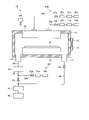
図1は、本開示の第1の実施形態における基板処理装置10の一例を示す概略断面図である。基板処理装置10は、例えば化学真空蒸着(CVD)により、被処理基板Wに有機膜を成膜する装置である。被処理基板Wは、例えば半導体ウエハである。
(First Embodiment)
[Structure of substrate processing device 10]
FIG. 1 is a schematic cross-sectional view showing an example of a
本実施形態では、2種類の原料Aおよび原料Bにより、被処理基板Wに有機膜が成膜される。例えば、被処理基板Wに成膜される有機膜がポリ尿素の有機膜である場合、原料Aは、例えばジイソシアネートモノマーであり、原料Bは、例えばジアミンモノマーである。原料Aは、第1のモノマーの一例であり、原料Bは、第2のモノマーの一例である。基板処理装置10を用いて、被処理基板Wの表面においてジイソシアネートおよびジアミンを蒸着重合させることによって、被処理基板Wの表面にポリ尿素の有機膜が成膜される。
In the present embodiment, the organic film is formed on the substrate W to be processed by the two types of raw materials A and B. For example, when the organic film formed on the substrate W to be treated is an organic film of polyurea, the raw material A is, for example, a diisocyanate monomer, and the raw material B is, for example, a diamine monomer. The raw material A is an example of the first monomer, and the raw material B is an example of the second monomer. An organic film of polyurea is formed on the surface of the substrate W to be treated by vapor-depositing and polymerizing diisocyanate and diamine on the surface of the substrate W to be treated using the
基板処理装置10は、チャンバ11、プラズマ発生装置30、排気管40、圧力調整バルブ41、排気装置42、制御装置100、および第1のガス供給部200を備える。プラズマ発生装置30は、エネルギー供給装置の一例である。排気管40は、第1の排気管の一例である。
The
チャンバ11は、真空雰囲気を区画する内壁を有する真空容器である。ここで、真空雰囲気は、例えば、中真空(100~0.1Pa)である。チャンバ11内には、被処理基板Wを載置する載置台15が設けられている。載置台15には、被処理基板Wの温度を制御するための図示しない温度制御機構が内蔵されている。当該温度制御機構により、被処理基板Wが原料Aおよび原料Bの重合反応に適した温度に制御される。
The
チャンバ11の側壁には、被処理基板Wを搬入および搬出するための開口12が形成されており、開口12は、ゲートバルブ13によって開閉可能となっている。また、チャンバ11の内壁には、当該内壁を加熱するためのヒータが埋め込まれている。当該ヒータによってチャンバ11の内壁が加熱されることにより、チャンバ11の内壁に付着するデポが低減される。
An
チャンバ11の上部には、第1のガス供給部200から供給された原料Aおよび原料Bの気体をチャンバ11内に供給するためのシャワーヘッド16が設けられている。シャワーヘッド16内には図示しないヒータが設けられており、当該ヒータによってシャワーヘッド16の内壁が加熱される。これにより、シャワーヘッド16内において原料Aおよび原料Bの気体の重合反応が抑制される。
A
また、チャンバ11の側壁の下方には、排気口14が設けられており、チャンバ11内のガスは、排気口14を介してチャンバ11の外部へ排気される。
Further, an
第1のガス供給部200は、原料供給源20a、原料供給源20b、気化器21a、気化器21b、流量制御器22a、流量制御器22b、バルブ23a、およびバルブ23bを有する。原料供給源20aは、第1の原料としての原料Aの液体を収容しており、液体の状態における原料Aを気化器21aに供給する。気化器21aは、原料供給源20aから供給される原料Aの液体を気化させる。気化器21aは、例えば図示しないヒータを有し、原料供給源20aから供給される原料Aの液体を加熱することにより気化させる。
The first
流量制御器22aは、気化器21aによって気化された原料Aの流量を制御する。バルブ23aは、流量制御器22aによって流量が制御された原料Aの気体のシャワーヘッド16への供給および供給遮断を制御する。バルブ23aを介して供給された原料Aの気体は、供給配管24aを介してシャワーヘッド16に供給される。供給配管24aには、供給配管24a内を流動する原料Aの気体の温度を調節する機構、例えば、供給配管24aを加熱するヒータが設けられている。
The
原料供給源20bは、第2の原料としての原料Bの液体を収容しており、液体の状態における原料Bを気化器21bに供給する。気化器21bは、原料供給源20bから供給される原料Bの液体を気化させる。気化器21bは、例えばヒータを有し、原料供給源20bから供給される原料Bの液体を加熱することにより気化させる。
The raw
流量制御器22bは、気化器21bによって気化された原料Bの流量を制御する。バルブ23bは、流量制御器22bによって流量が制御された原料Bの気体のシャワーヘッド16への供給および供給遮断を制御する。バルブ23bを介して供給された原料Bの気体は、供給配管24bを介してシャワーヘッド16に供給される。供給配管24bには、供給配管24b内を流動する原料Bの気体の温度を調節する機構、例えば、供給配管24bを加熱するヒータが設けられている。
The
なお、第1のガス供給部200からシャワーヘッド16を介してチャンバ11内に供給されるガスには、原料Aおよび原料Bの気体に加えて、N2ガスやArガス等の不活性ガスが添加されていてもよい。
The gas supplied from the first
排気口14には、排気管40を介して、圧力調整バルブ41および排気装置42が接続されている。排気装置42は、真空ポンプを有し、排気管40および圧力調整バルブ41を介してチャンバ11内のガスを排気する。圧力調整バルブ41は、開度を調整することにより、排気装置42による排気量を調整し、チャンバ11内の圧力を所定の圧力に制御する。
A
排気口14と圧力調整バルブ41との間の排気管40には、プラズマ発生装置30が設けられている。プラズマ発生装置30は、排気管40内を流れるガスに高周波電力を供給することにより、排気管40内を流れるガスをプラズマ化する。本実施形態において、プラズマ発生装置30は、誘導結合プラズマにより、排気管40内を流れるガスをプラズマ化する。
A
なお、他の形態として、プラズマ発生装置30は、誘導結合以外の方式のプラズマにより、排気管40内を流れるガスをプラズマ化してもよい。誘導結合以外の方式のプラズマとしては、例えば、容量結合型プラズマ(CCP)、マイクロ波励起表面波プラズマ(SWP)、電子サイクロトン共鳴プラズマ(ECP)、およびヘリコン波励起プラズマ(HWP)等が挙げられる。
As another form, the
制御装置100は、メモリ、プロセッサ、および入出力インターフェイスを有する。プロセッサは、メモリに格納されたプログラムやレシピを読み出して実行することにより、入出力インターフェイスを介して基板処理装置10の各部を制御する。制御装置100は、メモリに格納されたプログラムやレシピを読み出して実行することにより、入出力インターフェイスを介して、気化器21a、気化器21b、流量制御器22a、および流量制御器22bを制御する。また、制御装置100は、メモリに格納されたプログラムやレシピを読み出して実行することにより、入出力インターフェイスを介して、バルブ23a、バルブ23b、プラズマ発生装置30、圧力調整バルブ41、および排気装置42を制御する。
The
ここで、被処理基板Wに2種類のモノマーの重合体である有機膜を成膜する場合、シャワーヘッド16から2種類のモノマーを含むガスがチャンバ11内に供給される。しかし、チャンバ11内に供給されたガスに含まれるモノマーは、全てが反応に寄与するわけではないため、反応に寄与しなかったモノマーは、排気装置42によってチャンバ11内から排気される。
Here, when an organic film which is a polymer of two kinds of monomers is formed on the substrate W to be treated, a gas containing two kinds of monomers is supplied from the
チャンバ11内から排気されたモノマーは、排気経路を流れる過程で、排気経路に存在する部材の表面において重合反応により重合体のデポを形成する場合がある。圧力調整バルブ41や排気装置42等にデポが形成されると、圧力調整バルブ41や排気装置42の性能が劣化する。そのため、圧力調整バルブ41や排気装置42等を加熱することにより、重合反応を抑制することも考えられるが、加熱部材の配置による装置の大型化や消費電力の増大等の問題がある。
The monomer exhausted from the
そこで、本実施形態の基板処理装置10では、チャンバ11と排気装置42の間の排気経路上に、排気されるガスをプラズマ化するプラズマ発生装置30が設けられている。排気されるガスにプラズマ発生装置30によって生成されたプラズマを照射することにより、排気されるガスに含まれる、重合反応に寄与しなかった2種類のモノマー、即ち未反応成分の少なくともいずれか一方が、低分子化される。例えば、排気されるガスに含まれる、重合反応に寄与しなかった2種類のモノマーの少なくともいずれか一方の官能基が、脱官能基化(官能基が分解)される。これにより、排気経路上において、プラズマ発生装置30の下流側では、排気されたガスによる重合反応が抑制される。これにより、圧力調整バルブ41や排気装置42等に付着する重合体のデポを抑制することができ、圧力調整バルブ41や排気装置42等の性能劣化を抑制することができる。
Therefore, in the
なお、2種類のモノマーの少なくともいずれか一方の未反応成分が全て低分子化されなかったとしても、プラズマ発生装置30によるプラズマの照射がない場合に比べて、圧力調整バルブ41や排気装置42等に付着する重合体のデポの量を抑制することができる。これにより、圧力調整バルブ41や排気装置42等の部材のクリーニングの周期を長くすることができ、プロセスのスループットを向上させることができる。
Even if all the unreacted components of at least one of the two types of monomers are not reduced in molecular weight, the
以上、第1の実施形態について説明した。本実施形態における基板処理装置10は、チャンバ11と、第1のガス供給部200と、排気装置42と、排気管40と、プラズマ発生装置30とを備える。チャンバ11は、被処理基板Wを収容する。第1のガス供給部200は、第1のモノマーを含むガスと、第1のモノマーと重合反応することにより重合体を形成する第2のモノマーを含むガスとをチャンバ11内に供給することにより、被処理基板Wに重合体の膜を形成する。排気装置42は、チャンバ11内のガスを排気する。排気管40は、チャンバ11と排気装置42とを接続する。プラズマ発生装置30は、排気管40内を流れるガスにエネルギーを供給することにより、チャンバ11から排気されるガスに含まれる第1のモノマーおよび第2のモノマーの少なくともいずれか一方の未反応成分を低分子化する。これにより、圧力調整バルブ41や排気装置42等に付着する重合体のデポを抑制することができ、圧力調整バルブ41や排気装置42等の性能劣化を抑制することができる。
The first embodiment has been described above. The
また、上記した実施形態において、プラズマ発生装置30は、排気管40内を流れるガスに高周波電力を供給することにより生成されるプラズマによって排気管40内を流れるガスにエネルギーを供給することにより、チャンバ11から排気されるガスに含まれる第1のモノマーおよび第2のモノマーの少なくともいずれか一方の未反応成分を低分子化する。これにより、排気経路上において、プラズマ発生装置30の下流側では、排気されたガスによる重合反応が抑制される。
Further, in the above-described embodiment, the
(第2の実施形態)
第1の実施形態のプラズマ発生装置30は、チャンバ11内から排気されるガスのみを用いてプラズマを生成するため、排気管40内を流れるガスの条件によっては、プラズマを安定的に生成することが難しい場合がある。そこで、本実施形態のプラズマ発生装置30では、プラズマ発生装置30の上流の排気経路において、排気経路を流れるガスに、プラズマの安定的な生成を補助するためのガスが添加される。プラズマの安定的な生成を補助するためのガスとしては、例えばArガス等の不活性ガスが挙げられる。
(Second embodiment)
Since the
[基板処理装置10の構成]
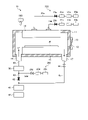
図2は、本開示の第2の実施形態における基板処理装置10の一例を示す概略断面図である。本実施形態における基板処理装置10は、例えば図2に示されるように、チャンバ11、プラズマ発生装置30、排気管40、圧力調整バルブ41、排気装置42、制御装置100、第1のガス供給部200、および第2のガス供給部201を備える。なお、以下に説明する点を除き、図2において、図1と同じ符号が付された構成は、図1において説明された構成と同一または同様の機能を有するため説明を省略する。
[Structure of substrate processing device 10]
FIG. 2 is a schematic cross-sectional view showing an example of the
第2のガス供給部201は、ガス供給源20c、流量制御器22c、およびバルブ23cを有する。ガス供給源20cは、例えばArガス等のプラズマの安定的な生成を補助するための添加ガスを供給する。流量制御器22cは、ガス供給源20cから供給されるガスの流量を制御する。バルブ23cは、流量制御器22cによって流量が制御されたガスの排気管40への供給および供給遮断を制御する。バルブ23cを介して供給された添加ガスは、供給配管24cを介して、排気口14とプラズマ発生装置30との間の排気管40内に供給される。
The second
プラズマ発生装置30は、チャンバ11から排気されたガスと、第2のガス供給部201から供給された添加ガスとの混合ガスに高周波電力を供給することにより、排気管40内を流れるガスをプラズマ化する。
The
以上、第2の実施形態について説明した。本実施形態における基板処理装置10は、チャンバ11とプラズマ発生装置30との間の排気管40内に不活性ガスを供給する第2のガス供給部201を備える。これにより、排気経路を流れるガスを用いて、プラズマをより安定的に生成することができる。そのため、排気されるガスに含まれる2種類のモノマーの少なくともいずれか一方の未反応成分のより多くを、低分子化することができ、圧力調整バルブ41や排気装置42等に付着する重合体のデポを効果的に抑制することができる。
The second embodiment has been described above. The
(第3の実施形態)
上記した第1および第2の実施形態におけるプラズマ発生装置30は、成膜処理時にチャンバ11から排気されるガスによって排気経路内に付着するデポを、プラズマを用いて低減する。これに対し、本実施形態のプラズマ発生装置30は、さらに、プラズマに含まれる活性種をチャンバ11内に供給することにより、重合反応によりチャンバ11内に付着したデポをクリーニングする。
(Third embodiment)
The
[基板処理装置10の構成]
図3は、本開示の第3の実施形態における基板処理装置10の一例を示す概略断面図である。本実施形態における基板処理装置10は、例えば図3に示されるように、チャンバ11、プラズマ発生装置30、排気管40、圧力調整バルブ41、排気装置42、制御装置100、第1のガス供給部200、および第3のガス供給部202を備える。また、本実施形態における基板処理装置10は、例えば図3に示されるように、バルブ43、バルブ44、および排気管45を備える。なお、以下に説明する点を除き、図3において、図1と同じ符号が付された構成は、図1において説明された構成と同一または同様の機能を有するため説明を省略する。
[Structure of substrate processing device 10]
FIG. 3 is a schematic cross-sectional view showing an example of the
チャンバ11の側壁の下方には、排気口14および排気口17が設けられており、チャンバ11内のガスは、排気口14および排気口17のいずれか一方を介してチャンバ11の外部へ排気される。
An
排気口17には、バルブ44を介して排気管45の一端が接続されている。排気管45の他端は、プラズマ発生装置30と圧力調整バルブ41との間の排気管40に接続されている。バルブ43は、排気管40と排気管45との接続位置とプラズマ発生装置30との間の排気管40に設けられている。バルブ43は、第1のバルブの一例であり、バルブ44は、第2のバルブの一例である。排気管45は、第2の排気管の一例である。
One end of the
第3のガス供給部202は、ガス供給源20d、流量制御器22d、およびバルブ23dを有する。ガス供給源20dは、クリーニングガスを供給する。クリーニングガスは、例えば酸素含有ガスである。本実施形態において、酸素含有ガスは、例えば不活性ガスとO2ガスの混合ガスである。不活性ガスは、例えばArガスである。なお、酸素含有ガスは、例えば不活性ガスとO3ガス等の混合ガスであってもよい。
The third
流量制御器22dは、ガス供給源20dから供給されるクリーニングガスの流量を制御する。バルブ23dは、流量制御器22dによって流量が制御されたクリーニングガスの排気管40への供給および供給遮断を制御する。バルブ23dを介して供給されたクリーニングガスは、供給配管24dを介して、プラズマ発生装置30とバルブ43との間の排気管40内に供給される。
The
基板処理装置10によって成膜処理が行われる場合、プラズマ発生装置30は、チャンバ11から排気されたガスに高周波電力を供給することにより、排気管40内を流れるガスをプラズマ化する。また、基板処理装置10によってクリーニング処理が行われる場合、プラズマ発生装置30は、第3のガス供給部202から供給されたクリーニングガスに高周波電力を供給することにより、クリーニングガスをプラズマ化する。
When the film forming process is performed by the
[成膜処理]
図4は、成膜処理時の各バルブの状態の一例を示す図である。基板処理装置10によって成膜処理が行われる場合、例えば図4に示さるように、バルブ23dおよびバルブ44が閉じられ、バルブ23a、バルブ23b、およびバルブ43が開かれる。なお、図4において、開かれているバルブは白抜きで描かれており、閉じられているバルブは黒塗りで描かれている。
[Film film processing]
FIG. 4 is a diagram showing an example of the state of each valve during the film forming process. When the film forming process is performed by the
これにより、原料Aおよび原料Bを含む気体が第1のガス供給部200からチャンバ11内に供給され、被処理基板W上に原料Aおよび原料Bの重合体の有機膜が成膜される。そして、成膜に寄与しなかった原料Aおよび原料Bを含むガスは、排気口14および排気管40を介してプラズマ発生装置30に供給され、プラズマ発生装置30によってプラズマ化される。これによって、排気ガスに含まれる原料Aおよび原料Bの未反応成分が低分子化され、排気される。
As a result, the gas containing the raw material A and the raw material B is supplied into the
[クリーニング処理]
図5は、クリーニング処理時の各バルブの状態の一例を示す図である。基板処理装置10によってクリーニング処理が行われる場合、例えば図5に示さるように、バルブ23a、バルブ23b、およびバルブ43が閉状態に制御され、バルブ23dおよびバルブ44が開状態に制御される。なお、図5において、開かれているバルブは白抜きで描かれており、閉じられているバルブは黒塗りで描かれている。また、クリーニング処理時には、載置台15の上面を保護するために、載置台15には、ダミーウエハW’が載置されることが好ましい。
[Cleaning process]
FIG. 5 is a diagram showing an example of the state of each valve during the cleaning process. When the cleaning process is performed by the
第3のガス供給部202は、クリーニングガスをプラズマ発生装置30に供給する。プラズマ発生装置30は、第3のガス供給部202から供給されたクリーニングガスに高周波電力を供給することにより、クリーニングガスをプラズマ化する。プラズマ化されたクリーニングガスに含まれる酸素ラジカル等の活性種は、排気管40および排気口14を介してチャンバ11内に供給される。チャンバ11内に供給された活性種により、チャンバ11、載置台15、およびシャワーヘッド16の表面に付着したデポが除去される。クリーニング処理では、チャンバ11内のガスは、排気口17からバルブ44および排気管45を介して排気される。
The third
[実験結果]
図6および図7は、クリーニングレートの実験結果の一例を示す図である。実験では、有機膜が成膜された被処理基板Wが載置台15上に載置され、図5に示されたように各バルブの状態が制御された。そして、プラズマ発生装置30によって生成されたプラズマに含まれる活性種による被処理基板W上の有機膜のエッチングレートがクリーニングレートとして測定された。実験の主な条件は、以下の通りである。
チャンバ11内の圧力:1[Torr]
処理時間:180[秒]
Ar/O2=500[sccm]/300[sccm]
[Experimental result]
6 and 7 are diagrams showing an example of the experimental results of the cleaning rate. In the experiment, the substrate W to be processed on which the organic film was formed was placed on the mounting table 15, and the state of each valve was controlled as shown in FIG. Then, the etching rate of the organic film on the substrate W to be treated by the active species contained in the plasma generated by the
Pressure in chamber 11: 1 [Torr]
Processing time: 180 [seconds]
Ar / O 2 = 500 [sccm] / 300 [sccm]
図6および図7に示されるように、被処理基板Wの温度が90℃~120℃のいずれであっても、被処理基板W上の有機膜がクリーニングされている。図6および図7の実験結果では、被処理基板Wの温度が高くなるほどクリーニングレートが高くなる傾向が見られた。従って、クリーニング処理の際には、チャンバ11内の温度を、成膜処理時の際の温度よりも高くすることにより、より効率よくデポを除去することができると考えられる。
As shown in FIGS. 6 and 7, the organic film on the substrate W to be processed is cleaned regardless of whether the temperature of the substrate W to be processed is 90 ° C to 120 ° C. In the experimental results of FIGS. 6 and 7, the cleaning rate tended to increase as the temperature of the substrate W to be processed increased. Therefore, it is considered that the depot can be removed more efficiently by raising the temperature in the
以上、第3の実施形態について説明した。本実施形態における基板処理装置10は、バルブ43と、バルブ44と、排気管45と、第3のガス供給部202とをさらに備える。バルブ43は、プラズマ発生装置30と排気装置42との間の排気管40に設けられる。バルブ44は、排気管45に設けられる。排気管45は、チャンバ11と排気装置42とを接続する。第3のガス供給部202は、プラズマ発生装置30とバルブ43との間の排気管40内に酸素含有ガスを供給する。被処理基板Wに重合体の膜を形成する場合、バルブ43が開かれ、バルブ44が閉じられ、チャンバ11から排気管40を介して排気装置42へ流れるガスにプラズマ発生装置30によって生成されたプラズマが照射される。また、チャンバ11内のクリーニングが行われる場合、バルブ43が閉じられ、バルブ44が開かれ、第3のガス供給部202から供給された酸素含有ガスがプラズマ発生装置30によってプラズマ化され、プラズマに含まれる活性種によってチャンバ11内がクリーニングされる。これにより、プラズマ発生装置30を用いて、排気経路へのデポの付着の抑制と、チャンバ11内のクリーニングとを実現することができる。
The third embodiment has been described above. The
また、上記した第3の実施形態において、酸素含有ガスには、O2ガスまたはO3ガスが含まれる。これにより、酸素含有ガスのプラズマに含まれる活性種により、チャンバ11内のデポを除去することができる。
Further, in the third embodiment described above, the oxygen-containing gas includes O 2 gas or O 3 gas. Thereby, the depot in the
[その他]
なお、本願に開示された技術は、上記した実施形態に限定されるものではなく、その要旨の範囲内で数々の変形が可能である。
[others]
The technique disclosed in the present application is not limited to the above-described embodiment, and many modifications can be made within the scope of the gist thereof.
例えば、上記した第1~第3の実施形態の基板処理装置10では、エネルギー供給装置の一例としてプラズマ発生装置30が用いられたが、開示の技術はこれに限られない。例えば、基板処理装置10には、エネルギー供給装置の他の例として、排気管40内を流れるガスに紫外線を照射する紫外線照射装置が用いられてもよい。
For example, in the
例えば、成膜処理の際、紫外線照射装置は、排気管40内を流れるガスに紫外線を照射することによって排気管40内を流れるガスにエネルギーを供給する。これにより、紫外線照射装置から照射された紫外線によって、チャンバ11から排気されるガスに含まれる第1のモノマーおよび第2のモノマーの少なくともいずれか一方の未反応成分が低分子化される。
For example, during the film forming process, the ultraviolet irradiation device supplies energy to the gas flowing in the
また、クリーニング処理の際、紫外線照射装置は、第3のガス供給部202から供給されたクリーニングガスに紫外線を照射することにより、活性種を生成し、生成された活性種によってチャンバ11内をクリーニングする。プラズマ発生装置30に代えて、紫外線照射装置が設けられることによっても、排気経路へのデポの付着の抑制と、チャンバ11内のクリーニングとを実現することができる。
Further, during the cleaning process, the ultraviolet irradiation device generates an active species by irradiating the cleaning gas supplied from the third
また、上記した第3の実施形態の基板処理装置10においても、上記した第2の実施形態の基板処理装置10と同様に、プラズマ発生装置30の上流の排気経路において、排気経路を流れるガスに、プラズマの安定的な生成を補助するためのガスが添加されてもよい。
Further, also in the
なお、今回開示された実施形態は全ての点で例示であって制限的なものではないと考えられるべきである。実に、上記した実施形態は多様な形態で具現され得る。また、上記の実施形態は、添付の特許請求の範囲およびその趣旨を逸脱することなく、様々な形態で省略、置換、変更されてもよい。 It should be noted that the embodiments disclosed this time are exemplary in all respects and are not restrictive. Indeed, the above embodiments can be embodied in a variety of forms. Moreover, the above-mentioned embodiment may be omitted, replaced or changed in various forms without departing from the scope of the attached claims and the purpose thereof.
W 被処理基板
W’ ダミーウエハ
10 基板処理装置
11 チャンバ
12 開口
13 ゲートバルブ
14 排気口
15 載置台
16 シャワーヘッド
17 排気口
200 第1のガス供給部
201 第2のガス供給部
202 第3のガス供給部
20a 原料供給源
21a 気化器
22a 流量制御器
23a バルブ
24a 供給配管
20b 原料供給源
21b 気化器
22b 流量制御器
23b バルブ
24b 供給配管
20c ガス供給源
22c 流量制御器
23c バルブ
24c 供給配管
20d ガス供給源
22d 流量制御器
23d バルブ
24d 供給配管
30 プラズマ発生装置
40 排気管
41 圧力調整バルブ
42 排気装置
43 バルブ
44 バルブ
45 排気管
100 制御装置
W Processed
Claims (4)
第1のモノマーを含むガスと、前記第1のモノマーと重合反応することにより重合体を形成する第2のモノマーを含むガスとを前記チャンバ内に供給することにより、前記被処理基板に前記重合体の膜を形成する第1のガス供給部と、
前記チャンバ内のガスを排気する排気装置と、
前記チャンバと前記排気装置とを接続する第1の排気管と、
前記第1の排気管内を流れるガスに高周波電力を供給することにより生成されるプラズマによって前記第1の排気管内を流れるガスにエネルギーを供給することにより、前記チャンバから排気されるガスに含まれる第1のモノマーおよび第2のモノマーの少なくともいずれか一方の未反応成分を低分子化するエネルギー供給装置と、
前記チャンバと前記排気装置とを接続する第2の排気管と、
前記エネルギー供給装置と前記排気装置との間の前記第1の排気管に設けられた第1のバルブと、
前記第2の排気管に設けられた第2のバルブと、
前記エネルギー供給装置と前記第1のバルブとの間の前記第1の排気管内に酸素含有ガスを供給する第3のガス供給部と
を備え、
前記被処理基板に前記重合体の膜を形成する場合、前記第1のバルブが開かれ、前記第2のバルブが閉じられ、前記チャンバから前記第1の排気管を介して前記排気装置へ流れるガスに前記エネルギー供給装置によって生成されたプラズマが照射され、
前記チャンバ内のクリーニングが行われる場合、前記第1のバルブが閉じられ、前記第2のバルブが開かれ、前記第3のガス供給部から供給された酸素含有ガスが前記エネルギー供給装置によってプラズマ化され、前記プラズマに含まれる活性種によって前記チャンバ内がクリーニングされることを特徴とする基板処理装置。 A chamber that houses the substrate to be processed and
By supplying the gas containing the first monomer and the gas containing the second monomer, which forms a polymer by polymerizing with the first monomer, into the chamber, the weight of the substrate to be treated is increased. A first gas supply unit that forms a coalesced film,
An exhaust device that exhausts the gas in the chamber,
A first exhaust pipe connecting the chamber and the exhaust device,
A first contained in the gas exhausted from the chamber by supplying energy to the gas flowing in the first exhaust pipe by plasma generated by supplying high frequency power to the gas flowing in the first exhaust pipe. An energy supply device for reducing the molecular weight of at least one of the unreacted components of the first monomer and the second monomer, and
A second exhaust pipe connecting the chamber and the exhaust device,
A first valve provided in the first exhaust pipe between the energy supply device and the exhaust device,
The second valve provided in the second exhaust pipe and
With a third gas supply unit that supplies oxygen-containing gas into the first exhaust pipe between the energy supply device and the first valve.
Equipped with
When the film of the polymer is formed on the substrate to be processed, the first valve is opened, the second valve is closed, and the gas flows from the chamber to the exhaust device through the first exhaust pipe. The gas is irradiated with the plasma generated by the energy supply device, and the gas is irradiated with the plasma.
When the inside of the chamber is cleaned, the first valve is closed, the second valve is opened, and the oxygen-containing gas supplied from the third gas supply unit is turned into plasma by the energy supply device. The substrate processing apparatus is characterized in that the inside of the chamber is cleaned by the active species contained in the plasma .
第1のモノマーを含むガスと、前記第1のモノマーと重合反応することにより重合体を形成する第2のモノマーを含むガスとを前記チャンバ内に供給することにより、前記被処理基板に前記重合体の膜を形成する第1のガス供給部と、
前記チャンバ内のガスを排気する排気装置と、
前記チャンバと前記排気装置とを接続する第1の排気管と、
前記第1の排気管内を流れるガスに紫外線を照射することによって前記第1の排気管内を流れるガスにエネルギーを供給することにより、前記チャンバから排気されるガスに含まれる第1のモノマーおよび第2のモノマーの少なくともいずれか一方の未反応成分を低分子化するエネルギー供給装置と、
前記チャンバと前記排気装置とを接続する第2の排気管と、
前記エネルギー供給装置と前記排気装置との間の前記第1の排気管に設けられた第1のバルブと、
前記第2の排気管に設けられた第2のバルブと、
前記エネルギー供給装置と前記第1のバルブとの間の前記第1の排気管内に酸素含有ガスを供給する第3のガス供給部と
を備え、
前記被処理基板に前記重合体の膜を形成する場合、前記第1のバルブが開かれ、前記第2のバルブが閉じられ、前記チャンバから前記第1の排気管を介して前記排気装置へ流れるガスに前記エネルギー供給装置から紫外線が照射され、
前記チャンバ内のクリーニングが行われる場合、前記第1のバルブが閉じられ、前記第2のバルブが開かれ、前記第3のガス供給部から供給された酸素含有ガスが前記エネルギー供給装置から照射された紫外線により生成された活性種によって前記チャンバ内がクリーニングされることを特徴とする基板処理装置。 A chamber that houses the substrate to be processed and
By supplying the gas containing the first monomer and the gas containing the second monomer, which forms a polymer by polymerizing with the first monomer, into the chamber, the weight of the substrate to be treated is increased. A first gas supply unit that forms a coalesced film,
An exhaust device that exhausts the gas in the chamber,
A first exhaust pipe connecting the chamber and the exhaust device,
The first monomer and the second monomer contained in the gas exhausted from the chamber by supplying energy to the gas flowing in the first exhaust pipe by irradiating the gas flowing in the first exhaust pipe with ultraviolet rays . An energy supply device that reduces the molecular weight of at least one of the unreacted components of the monomer of
A second exhaust pipe connecting the chamber and the exhaust device,
A first valve provided in the first exhaust pipe between the energy supply device and the exhaust device,
The second valve provided in the second exhaust pipe and
With a third gas supply unit that supplies oxygen-containing gas into the first exhaust pipe between the energy supply device and the first valve.
Equipped with
When the polymer film is formed on the substrate to be processed, the first valve is opened, the second valve is closed, and the gas flows from the chamber to the exhaust device through the first exhaust pipe. The gas is irradiated with ultraviolet rays from the energy supply device, and the gas is irradiated with ultraviolet rays.
When the inside of the chamber is cleaned, the first valve is closed, the second valve is opened, and the oxygen-containing gas supplied from the third gas supply unit is irradiated from the energy supply device. A substrate processing apparatus characterized in that the inside of the chamber is cleaned by an active species generated by ultraviolet rays .
Priority Applications (5)
| Application Number | Priority Date | Filing Date | Title |
|---|---|---|---|
| JP2018166546A JP7080140B2 (en) | 2018-09-06 | 2018-09-06 | Board processing equipment |
| TW108131165A TWI780354B (en) | 2018-09-06 | 2019-08-30 | Substrate processing device |
| KR1020190108765A KR102492099B1 (en) | 2018-09-06 | 2019-09-03 | Substrate processing apparatus |
| US16/560,151 US11081321B2 (en) | 2018-09-06 | 2019-09-04 | Substrate processing apparatus |
| CN201910842127.0A CN110880463B (en) | 2018-09-06 | 2019-09-06 | Substrate processing apparatus |
Applications Claiming Priority (1)
| Application Number | Priority Date | Filing Date | Title |
|---|---|---|---|
| JP2018166546A JP7080140B2 (en) | 2018-09-06 | 2018-09-06 | Board processing equipment |
Publications (2)
| Publication Number | Publication Date |
|---|---|
| JP2020038947A JP2020038947A (en) | 2020-03-12 |
| JP7080140B2 true JP7080140B2 (en) | 2022-06-03 |
Family
ID=69719686
Family Applications (1)
| Application Number | Title | Priority Date | Filing Date |
|---|---|---|---|
| JP2018166546A Active JP7080140B2 (en) | 2018-09-06 | 2018-09-06 | Board processing equipment |
Country Status (5)
| Country | Link |
|---|---|
| US (1) | US11081321B2 (en) |
| JP (1) | JP7080140B2 (en) |
| KR (1) | KR102492099B1 (en) |
| CN (1) | CN110880463B (en) |
| TW (1) | TWI780354B (en) |
Families Citing this family (3)
| Publication number | Priority date | Publication date | Assignee | Title |
|---|---|---|---|---|
| TWI783382B (en) * | 2020-03-18 | 2022-11-11 | 日商國際電氣股份有限公司 | Substrate processing apparatus, exhaust apparatus, and manufacturing method of semiconductor device |
| US20220033260A1 (en) * | 2020-07-29 | 2022-02-03 | Illinois Tool Works Inc. | Systems and methods for ozone degradation for a plasma treatment system |
| US20230390811A1 (en) * | 2022-06-06 | 2023-12-07 | Applied Materials, Inc. | Throttle valve and foreline cleaning using a microwave source |
Citations (5)
| Publication number | Priority date | Publication date | Assignee | Title |
|---|---|---|---|---|
| JP2000021867A (en) | 1998-07-07 | 2000-01-21 | Ulvac Corp | Semiconductor manufacturing apparatus and method of cleaning the apparatus |
| JP2003273081A (en) | 2002-03-14 | 2003-09-26 | Shibaura Mechatronics Corp | Plasma processing apparatus |
| JP2004237162A (en) | 2003-02-04 | 2004-08-26 | Seiko Epson Corp | Gas treatment device and method for producing semiconductor device |
| JP2010199497A (en) | 2009-02-27 | 2010-09-09 | Semiconductor Energy Lab Co Ltd | Apparatus for manufacturing semiconductor device and method for manufacturing semiconductor device |
| WO2010103953A1 (en) | 2009-03-13 | 2010-09-16 | 東京エレクトロン株式会社 | Substrate processing apparatus, trap device, method for controlling substrate processing apparatus, and method for controlling trap device |
Family Cites Families (17)
| Publication number | Priority date | Publication date | Assignee | Title |
|---|---|---|---|---|
| EP0173715B1 (en) * | 1984-02-13 | 1992-04-22 | SCHMITT, Jerome J. III | Method and apparatus for the gas jet deposition of conducting and dielectric thin solid films and products produced thereby |
| JPH05132759A (en) * | 1991-11-08 | 1993-05-28 | Ulvac Japan Ltd | Vapor-deposition polymerization device |
| JP2872637B2 (en) * | 1995-07-10 | 1999-03-17 | アプライド マテリアルズ インコーポレイテッド | Microwave plasma based applicator |
| JPH09306892A (en) * | 1996-05-14 | 1997-11-28 | Hitachi Ltd | Cleaning method and semiconductor manufacturing apparatus |
| JPH1070110A (en) * | 1997-07-07 | 1998-03-10 | Hitachi Ltd | Dry-etching method |
| JP4019258B2 (en) * | 2002-06-25 | 2007-12-12 | 日本電気株式会社 | Method for producing copolymerized polymer film |
| JP4113755B2 (en) * | 2002-10-03 | 2008-07-09 | 東京エレクトロン株式会社 | Processing equipment |
| JP2005085956A (en) * | 2003-09-08 | 2005-03-31 | Mitsubishi Heavy Ind Ltd | Cleaning method and cvd apparatus |
| JP2005307274A (en) * | 2004-04-21 | 2005-11-04 | Ebara Corp | Substrate treatment device |
| US20070267143A1 (en) * | 2006-05-16 | 2007-11-22 | Applied Materials, Inc. | In situ cleaning of CVD system exhaust |
| JP5277161B2 (en) | 2007-04-16 | 2013-08-28 | 株式会社アルバック | Polyurea film and method for forming the same |
| JP5179389B2 (en) * | 2008-03-19 | 2013-04-10 | 東京エレクトロン株式会社 | Shower head and substrate processing apparatus |
| US20090246399A1 (en) * | 2008-03-28 | 2009-10-01 | Asm Japan K.K. | Method for activating reactive oxygen species for cleaning carbon-based film deposition |
| SG10201601916TA (en) * | 2011-03-28 | 2016-04-28 | Applied Materials Inc | Method and apparatus for the selective deposition of epitaxial germanium stressor alloys |
| KR101870491B1 (en) * | 2014-03-11 | 2018-06-22 | 도쿄엘렉트론가부시키가이샤 | Plasma processing appratus, substrate processing system, fabrication method of thin film transistor, and storage medium |
| JP6349796B2 (en) * | 2014-03-11 | 2018-07-04 | 東京エレクトロン株式会社 | Plasma processing apparatus, thin film transistor manufacturing method, and storage medium |
| KR102477302B1 (en) * | 2015-10-05 | 2022-12-13 | 주성엔지니어링(주) | Substrate treatment apparatus having exhaust gas cracker and exhaust gas treatment method of the same |
-
2018
- 2018-09-06 JP JP2018166546A patent/JP7080140B2/en active Active
-
2019
- 2019-08-30 TW TW108131165A patent/TWI780354B/en active
- 2019-09-03 KR KR1020190108765A patent/KR102492099B1/en active IP Right Grant
- 2019-09-04 US US16/560,151 patent/US11081321B2/en active Active
- 2019-09-06 CN CN201910842127.0A patent/CN110880463B/en active Active
Patent Citations (5)
| Publication number | Priority date | Publication date | Assignee | Title |
|---|---|---|---|---|
| JP2000021867A (en) | 1998-07-07 | 2000-01-21 | Ulvac Corp | Semiconductor manufacturing apparatus and method of cleaning the apparatus |
| JP2003273081A (en) | 2002-03-14 | 2003-09-26 | Shibaura Mechatronics Corp | Plasma processing apparatus |
| JP2004237162A (en) | 2003-02-04 | 2004-08-26 | Seiko Epson Corp | Gas treatment device and method for producing semiconductor device |
| JP2010199497A (en) | 2009-02-27 | 2010-09-09 | Semiconductor Energy Lab Co Ltd | Apparatus for manufacturing semiconductor device and method for manufacturing semiconductor device |
| WO2010103953A1 (en) | 2009-03-13 | 2010-09-16 | 東京エレクトロン株式会社 | Substrate processing apparatus, trap device, method for controlling substrate processing apparatus, and method for controlling trap device |
Also Published As
| Publication number | Publication date |
|---|---|
| KR102492099B1 (en) | 2023-01-27 |
| CN110880463A (en) | 2020-03-13 |
| US11081321B2 (en) | 2021-08-03 |
| CN110880463B (en) | 2024-07-30 |
| TW202016332A (en) | 2020-05-01 |
| JP2020038947A (en) | 2020-03-12 |
| TWI780354B (en) | 2022-10-11 |
| KR20200028306A (en) | 2020-03-16 |
| US20200083029A1 (en) | 2020-03-12 |
Similar Documents
| Publication | Publication Date | Title |
|---|---|---|
| JP7079686B2 (en) | Film formation method and film formation equipment | |
| US9340879B2 (en) | Substrate processing apparatus, method for manufacturing semiconductor device and computer-readable recording medium | |
| JP7080140B2 (en) | Board processing equipment | |
| KR101701024B1 (en) | High growth rate process for conformal aluminum nitride | |
| TWI806323B (en) | System, method and device for processing target body | |
| KR102648956B1 (en) | Method for cleaning components of plasma processing apparatus | |
| TWI591201B (en) | Film forming apparatus, film forming method, and non-transitory computer-readable storage medium | |
| US20150259799A1 (en) | Vertical heat treatment apparatus, method of operating vertical heat treatment apparatus, and storage medium | |
| KR102626138B1 (en) | Method for processing target object | |
| WO2010024036A1 (en) | Plasma processing device and method for cleaning plasma processing device | |
| JP6763274B2 (en) | Film forming equipment, cleaning method of film forming equipment and storage medium | |
| JP2020065079A (en) | Plasma processing device and method for exposure to atmosphere | |
| US20230230811A1 (en) | Surface modification for metal-containing photoresist deposition | |
| JP5715361B2 (en) | Cleaning method | |
| JP2012169409A (en) | Semiconductor manufacturing device and semiconductor device manufacturing method | |
| WO2021092197A1 (en) | Plasma-enhanced atomic layer deposition with radio-frequency power ramping | |
| KR20210049173A (en) | Etching method | |
| JP2016164932A (en) | Method and device for forming silicon nitride film | |
| JP2023529359A (en) | In-feature wet etch rate ratio reduction | |
| JP2021141285A (en) | Semiconductor manufacturing apparatus and manufacturing method for semiconductor device | |
| KR102125473B1 (en) | Deposition Method of Thin Film | |
| JP2020167186A (en) | Plasma etching device and plasma etching method | |
| WO2024053386A1 (en) | Substrate treatment system | |
| TWI850625B (en) | Plasma treatment device and plasma treatment method | |
| JP2010272551A (en) | Substrate treating device, and method of treating substrate |
Legal Events
| Date | Code | Title | Description |
|---|---|---|---|
| A621 | Written request for application examination |
Free format text: JAPANESE INTERMEDIATE CODE: A621 Effective date: 20210303 |
|
| A977 | Report on retrieval |
Free format text: JAPANESE INTERMEDIATE CODE: A971007 Effective date: 20211224 |
|
| A131 | Notification of reasons for refusal |
Free format text: JAPANESE INTERMEDIATE CODE: A131 Effective date: 20220104 |
|
| A521 | Request for written amendment filed |
Free format text: JAPANESE INTERMEDIATE CODE: A523 Effective date: 20220225 |
|
| TRDD | Decision of grant or rejection written | ||
| A01 | Written decision to grant a patent or to grant a registration (utility model) |
Free format text: JAPANESE INTERMEDIATE CODE: A01 Effective date: 20220426 |
|
| A61 | First payment of annual fees (during grant procedure) |
Free format text: JAPANESE INTERMEDIATE CODE: A61 Effective date: 20220524 |
|
| R150 | Certificate of patent or registration of utility model |
Ref document number: 7080140 Country of ref document: JP Free format text: JAPANESE INTERMEDIATE CODE: R150 |