JP5268436B2 - Optical filter and imaging device - Google Patents
Optical filter and imaging device Download PDFInfo
- Publication number
- JP5268436B2 JP5268436B2 JP2008149637A JP2008149637A JP5268436B2 JP 5268436 B2 JP5268436 B2 JP 5268436B2 JP 2008149637 A JP2008149637 A JP 2008149637A JP 2008149637 A JP2008149637 A JP 2008149637A JP 5268436 B2 JP5268436 B2 JP 5268436B2
- Authority
- JP
- Japan
- Prior art keywords
- optical member
- multilayer film
- optical
- optical filter
- image sensor
- Prior art date
- Legal status (The legal status is an assumption and is not a legal conclusion. Google has not performed a legal analysis and makes no representation as to the accuracy of the status listed.)
- Expired - Fee Related
Links
Images


Classifications
-
- G—PHYSICS
- G02—OPTICS
- G02B—OPTICAL ELEMENTS, SYSTEMS OR APPARATUS
- G02B5/00—Optical elements other than lenses
- G02B5/20—Filters
-
- G—PHYSICS
- G02—OPTICS
- G02B—OPTICAL ELEMENTS, SYSTEMS OR APPARATUS
- G02B5/00—Optical elements other than lenses
- G02B5/20—Filters
- G02B5/28—Interference filters
- G02B5/285—Interference filters comprising deposited thin solid films
-
- G—PHYSICS
- G02—OPTICS
- G02B—OPTICAL ELEMENTS, SYSTEMS OR APPARATUS
- G02B1/00—Optical elements characterised by the material of which they are made; Optical coatings for optical elements
- G02B1/10—Optical coatings produced by application to, or surface treatment of, optical elements
- G02B1/11—Anti-reflection coatings
- G02B1/113—Anti-reflection coatings using inorganic layer materials only
- G02B1/115—Multilayers
Landscapes
- Physics & Mathematics (AREA)
- General Physics & Mathematics (AREA)
- Optics & Photonics (AREA)
- Optical Filters (AREA)
- Surface Treatment Of Optical Elements (AREA)
- Blocking Light For Cameras (AREA)
- Studio Devices (AREA)
Abstract
Description
本発明は、撮影レンズと撮像素子の間に配置され、該撮像素子に導かれる光束の高周波成分を減衰するとともに、光束の赤外波長成分をカットするのに好適な光学フィルタ及び撮像装置に関する。 The present invention relates to an optical filter and an imaging apparatus that are disposed between a photographing lens and an imaging device and are suitable for attenuating a high-frequency component of a light beam guided to the imaging device and cutting an infrared wavelength component of the light beam.
従来からデジタルカメラ等の撮像装置において、ローパスフィルタ及び赤外吸収フィルタを有する光学フィルタが撮像素子の前面に配置されている。ローパスフィルタは、CCDやCMOS等よりなる撮像素子における被写界像の擬似信号による偽色発生を抑制する。また、赤外吸収フィルタは、撮像素子の感度を人間の視感度に近似させる。 Conventionally, in an imaging apparatus such as a digital camera, an optical filter having a low-pass filter and an infrared absorption filter is disposed on the front surface of the imaging element. The low-pass filter suppresses the generation of false colors due to the pseudo signal of the object scene image in the image sensor made up of CCD, CMOS, or the like. The infrared absorption filter approximates the sensitivity of the image sensor to human visibility.
このようにした光学フィルタの最前面は、空気中に露呈しているために、浮遊する塵埃やカメラ内部で発生する塵等の異物が付着してしまうことは避けられない。その結果、撮像された画像に該異物が映り込んでしまい、画像としての品位を低下させることがあった。 Since the forefront of the optical filter thus formed is exposed to the air, it is inevitable that foreign matters such as floating dust and dust generated inside the camera will adhere. As a result, the foreign matter is reflected in the captured image, and the quality of the image may be reduced.
そこで、光学フィルタへの異物付着を予防したり、光学フィルタに付着した異物を除去したりするためには、以下の方式を用いることが有効である。
(1)光学フィルタに振動を加えて異物を振り落とす。
(2)光学フィルタの静電気を除去することで、異物付着を防止する。
(3)光学フィルタ表面に異物が付着しにくいコートを施す。
Therefore, in order to prevent foreign matters from adhering to the optical filter or to remove foreign matters adhering to the optical filter, it is effective to use the following method.
(1) Apply vibration to the optical filter to shake off foreign matter.
(2) Preventing adhesion of foreign matters by removing static electricity from the optical filter.
(3) Apply a coating on the surface of the optical filter to prevent foreign matter from adhering
ここで、(1)の光学ローパスフィルタに付着した異物を振り落とす方式に関しては、特許文献1等において、光学ローパスフィルタを圧電素子と密着配置し、光学ローパスフィルタを圧電素子の伸縮運動に追従させる提案がなされている。 Here, regarding the method (1) of shaking off the foreign matter attached to the optical low-pass filter, in Patent Document 1 or the like, the optical low-pass filter is placed in close contact with the piezoelectric element, and the optical low-pass filter follows the expansion and contraction motion of the piezoelectric element. Proposals have been made.
(2)の光学フィルタに静電気による電荷が溜まらないようにする方式に関しては、特許文献2において、光学フィルタの反射防止膜の表面から二層目以上の少なくとも一層をITO(スズドープ酸化インジウム)等の導電性膜で構成する提案がなされている。同様に、特許文献3においても、ITO膜を生成し、コート層表面の導電性を高める提案がなされている。 Regarding the method (2) for preventing electric charges from accumulating in the optical filter, in Patent Document 2, at least one second layer or more from the surface of the antireflection film of the optical filter is made of ITO (tin-doped indium oxide) or the like. There have been proposals for the construction of a conductive film. Similarly, Patent Document 3 proposes to generate an ITO film and increase the conductivity of the surface of the coat layer.
(3)の光学フィルタ表面に異物が付着しにくいコートを施す方式に関しては、特許文献4において、フッ素を含んだ高分子材料、或いはMgF2(フッ化マグネシウム)のコートを施すことが提案されている。これにより、光学フィルタの表面エネルギーを下げ、エアブロアー等を利用してゴミを落とし易くすることができる。 Regarding the method of applying a coating that does not allow foreign matter to adhere to the optical filter surface in (3), Patent Document 4 proposes to apply a fluorine-containing polymer material or MgF 2 (magnesium fluoride) coating. Yes. Thereby, the surface energy of the optical filter can be lowered, and dust can be easily removed using an air blower or the like.
一般的に撮像素子の画素に対応したカラーフィルタの配列は、RGBGの4画素からなるベイヤー配列を基本としている。光学ローパスフィルタにスポットの1点ビームを入射させたとき、4点のビームに分離する、いわゆる4点点像分離を行うことによって撮影画像における偽色の発生を軽減している。 In general, the color filter array corresponding to the pixels of the image sensor is based on a Bayer array including four RGBG pixels. Generation of false colors in the photographed image is reduced by performing so-called four-point point image separation, which separates the four-point beam when a spot one-point beam is incident on the optical low-pass filter.
図14は、4点点像分離を行うために4枚の光学部材を貼り合わせた一般的な光学フィルタの構成を示したものである。300は水晶等の複屈折材料であり、水平方向に2点分離するための回転角0°の複屈折水晶板が用いられる。301は赤外吸収フィルタであり、CCD等の撮像素子の分光感度と人間の視感度を概一致させるためのものである。302は水晶からなる偏光解消板(λ/4波長板)であり、複屈折水晶板300を通過することで直線偏光となった被写界光束の偏光解消を行う。303は回転角90°の複屈折水晶板であり、被写界光束が複屈折水晶板303を通ることで上下方向に点像分離がなされる。かかる光学フィルタにより、撮像素子106には最終的には4点分離の被写界光束が入射することとなり、撮影画像の偽色発生を軽減している。なお、309は撮像素子106の受光部106aをパッケージ部106b内部に封止するためのカバーガラスである。
FIG. 14 shows a configuration of a general optical filter in which four optical members are bonded to perform four-point image separation.
通常、撮影レンズ側の複屈折水晶板300の表面には、40層程度のUV−IRカットコート401が配され、赤外吸収フィルタ301の波長吸収特性との相互作用により、撮像素子106に入射する所望の分光透過率が得られるようになっている。さらに、被写界光路において各媒質の界面における反射光を低減するために、複屈折水晶板303の撮像素子側の面及びカバーガラス309の両面に反射防止のためのARコート402が配される。
Usually, a UV-
ここで、UV−IRカットコート401は、その層数が多いこともあって、蒸着を行う蒸着器内の壁に付着した不要な蒸着物質の清掃を行うタイミングは、光学性能維持、生産効率の面で非常に重要である。また、UV−IRカットコート、ARコートには、通常SiO2、TiO2といった蒸着物質を用いるが、フッ素系材料は基本的に樹脂であり、これらの蒸着物質の蒸着条件となる蒸着対象物の基板温度、蒸着材料の加熱温度等が両者の蒸着において大幅に異なる。そのため、一回の工程で蒸着を行うのは生産効率上困難を伴う。さらに、フッ素系材料の蒸着を行った後に、蒸着器内壁に付着した同物質が次回以降の蒸着に影響を与えないように、通常よりもいっそう頻繁に内壁の清掃を行う必要がある。もしも清掃を怠るならば、SiO2、TiO2といった蒸着材料へのフッ素系材料の混入により、ヘイズ(曇り)の増加、分光の異常、欠陥の増加といった性能低下を引き起こすことになるからである。また、清掃の回数増は、直接ローパスフィルタのコスト増という問題にも直結している。
Here, the UV-
一方、静電気による異物付着を避けるために、光学フィルタ上に静電気による電荷が溜まらなくするよう、光学基材に透明性導電膜(ITO膜)を蒸着するという方式がある。しかしながら、透明性導電膜の蒸着を、光学薄膜を蒸着する一般的な機器である真空蒸着器で行うためには、その釜内部を酸素雰囲気下にする必要がある等の制約を伴う。そこで、透明性導電膜の蒸着方法は一般的にスパッタリング法にて行われており、透明性導電膜を蒸着するだけのために専用の蒸着器を工程内に設置する必要があった。 On the other hand, there is a method of depositing a transparent conductive film (ITO film) on an optical substrate so as to prevent static charges from accumulating on the optical filter in order to avoid foreign matter adhesion due to static electricity. However, in order to perform the deposition of the transparent conductive film with a vacuum deposition apparatus, which is a general device for depositing an optical thin film, there is a restriction that the interior of the kettle needs to be in an oxygen atmosphere. Therefore, the vapor deposition method of the transparent conductive film is generally performed by a sputtering method, and it is necessary to install a dedicated vapor deposition device in the process only for vapor deposition of the transparent conductive film.
以上のことから、光学フィルタの撮影レンズ側の面において、透明性導電膜を使用せずに静電気が溜まらない蒸着膜構成であって、かつ、その最表層に異物付着防止膜を設けることで異物の付着を低減することのできる光学フィルタを高品質、低コストで製造できる蒸着膜構成が望まれていた。 From the above, the surface of the optical filter on the photographic lens side has a vapor deposition film configuration that does not use a transparent conductive film and does not accumulate static electricity, and is provided with a foreign matter adhesion prevention film on the outermost layer. Therefore, there has been a demand for a vapor deposition film configuration that can produce an optical filter that can reduce the adhesion of the film with high quality and low cost.
本発明の光学フィルタは、撮像素子の前に配置される光学フィルタであって、前記光学フィルタは、第一の光学部材と、前記第一の光学部材よりも前記撮像素子側に配置され、赤外成分を吸収する第二の光学部材と、前記第一の光学部材の入射面を露出させるとともに、前記第一の光学部材の射出面と前記第二の光学部材の入射面までの間に密閉空間が形成されるように前記第一の光学部材と前記第二の光学部材とを保持する保持部材とを備え、前記第一の光学部材の入射面に導電性を有する反射防止多層膜を成膜し、前記密閉空間内となる面に、赤外光及び紫外光を遮断するダイクロイック多層膜を成膜し、前記反射防止多層膜の層数は前記ダイクロイック多層膜の層数よりも少なく構成され、前記反射防止多層膜の最表層にフッ素を含む材料からなる膜を成膜し、前記反射防止多層膜は、ポーラス状に成膜されたSiO2及びTiO2から構成されることを特徴とする。 The optical filter of the present invention is an optical filter disposed in front of the image sensor, and the optical filter is disposed on the image sensor side of the first optical member and the first optical member. The second optical member that absorbs an external component and the incident surface of the first optical member are exposed and sealed between the exit surface of the first optical member and the incident surface of the second optical member. A holding member for holding the first optical member and the second optical member so that a space is formed, and an antireflection multilayer film having conductivity is formed on the incident surface of the first optical member. A dichroic multilayer film that blocks infrared light and ultraviolet light is formed on the surface that is in the sealed space, and the number of layers of the antireflection multilayer film is less than the number of layers of the dichroic multilayer film. The outermost layer of the antireflection multilayer film contains fluorine Film is formed consisting of fees, the antireflection multilayer film is composed of SiO2 and TiO2 that was deposited in the porous characterized Rukoto.
本発明によれば、光学フィルタの撮影レンズ側の面において静電気を帯びにくくなり、異物の付着を低減することができる。それでも付着した異物は、異物付着防止膜を最表層に設けている効果によって、第一の光学部材の振動による異物除去動作や、撮影者自らエアーブローをかけることにより容易に除去可能である。さらに、静電気の問題を気にすることなく、赤外光及び紫外光カット効果を有するダイクロイック多層膜を、良好な分光特性かつ高信頼性のコーティングにて配することができる。以上のように、本発明によれば、光学フィルタを高品質、低コストで製造することが可能となる。 According to the present invention, the surface of the optical filter on the photographing lens side is less likely to be charged with static electricity, and foreign matter can be reduced. The foreign matter still attached can be easily removed by the foreign matter removal operation by the vibration of the first optical member or the photographer himself applying air blow due to the effect that the foreign matter adhesion preventing film is provided on the outermost layer. Furthermore, a dichroic multilayer film having an infrared light and ultraviolet light cut effect can be provided with a coating having good spectral characteristics and high reliability without worrying about the problem of static electricity. As described above, according to the present invention, an optical filter can be manufactured with high quality and low cost.
以下、添付図面を参照して、本発明の好適な実施形態について説明する。
(第1の実施の形態)
図1は、本発明を適用した第1の実施形態のデジタル一眼レフカメラの概略構成を示す図である。同図において、101はCPU(中央演算処理装置)であり、本デジタルカメラの動作を制御する。
Preferred embodiments of the present invention will be described below with reference to the accompanying drawings.
(First embodiment)
FIG. 1 is a diagram showing a schematic configuration of a digital single-lens reflex camera according to a first embodiment to which the present invention is applied. In the figure,
105は撮影レンズであり、撮影被写界光を撮像素子106上に結像させる。撮影レンズ105は、カメラの本体に着脱可能なレンズユニットに内蔵されている。106はCCDに代表される撮像素子である。133は撮影レンズ105から撮像素子106に到達する撮影被写界の光量を制御するフォーカルプレーンシャッタである。
121は半透過メインミラー、122はサブミラーであり、撮影被写界光はその一部が半透過メインミラー121、サブミラー122によって公知の位相差方式焦点検出ユニットに導かれる。これにより、撮影レンズ105にて結像された被写界光のピントが撮像素子106の受光面に対してどの方向に、どれ位ずれているか、いわゆるデフォーカス量として検出することができる。位相差方式焦点検出ユニットにおいて、123はフィールドレンズ、124は2次結像レンズ、119は焦点検出用のCCDラインセンサであり、ファインダ画面上の縦横3×5の計15ヶ所からなる領域の焦点検出が可能となっている。
125はレンズユニット内に設けられた撮影レンズ駆動制御部である。上記算出されたデフォーカス量に対して、撮影レンズ105のレンズ駆動敏感度(レンズ固有の制御の細かさ)を考慮し、CPU101は撮影レンズ駆動制御部125に撮影レンズ105の駆動させるための駆動量パルスを送る。撮影レンズ駆動制御部125は、送られてきたパルスに応じてパルスモータを駆動させ、撮影レンズ105を合焦位置に駆動させることで自動焦点調節を行う。
A photographing lens
126は接眼レンズ、127は像反転させるための光学反転手段であるペンタプリズム、128は撮影レンズ105の撮像素子106結像面と等価の結像面に置かれたピント板である。撮影レンズ105を通った被写界光は、半透過メインミラー121で反射されピント板128に結像する。ペンタプリズム127、接眼レンズ126を通じてカメラの撮影者はピント板128に結像した被写界像を見ることのできる、いわゆるTTL方式の光学ファインダ構成となっている。
126 is an eyepiece lens, 127 is a pentaprism which is an optical reversing means for reversing the image, and 128 is a focusing plate placed on an imaging surface equivalent to the imaging surface of the
130は結像レンズ、131は撮影被写界の可視光の輝度を測定する測光センサである。結像レンズ130によって、ピント板128上に結像された被写界像が測光センサ131上に2次結像される。測光センサ131は、縦×横、各々3×5に分割された受光領域を有しており、カメラのファインダ視野(被写界領域)の主要領域を3×5の領域に分割して測光することができる。
Fは光学フィルタであり、撮影レンズ105と撮像素子106の間に配置され、該撮像素子106に導かれる光束の高周波成分を減衰するとともに、光束の赤外波長成分をカットする。光学フィルタFは、詳しくは後述するが、複数の光学部材300〜303から構成される。撮影レンズ105側に配置された複屈折水晶板300は、外部から振動が与えられることで表面に付着した塵埃等の異物の除去を行う。
F is an optical filter which is disposed between the photographing
132はTFTカラー液晶からなる外部表示部である。
撮影者がレリーズSW114(図2を参照)を押下すると、メインミラー121は撮影レンズ105の光路外に退避し、撮影レンズ105によって集光された被写界光はフォーカルプレーンシャッタ133で光量制御がなされる。そして、撮像素子106によって被写界像として光電変換処理表示された後、画像データとしてフラッシュメモリ等の記録媒体に記録される。一方では、撮影済み画像として表示部132に表示される。
When the photographer presses the release SW 114 (see FIG. 2), the
図2は、第1の実施形態のデジタル一眼レフカメラの概略構成を示す電気ブロック図であり、図1に示した構成要素と同一のものには同一の符号を付して説明する。CPU101には、制御プログラムを記憶しているROM(リードオンリーメモリ)102、RAM(ランダムアクセスメモリ)103、データ格納手段104、画像処理部108、振動制御部109、LCD制御部111、レリーズSW114、DC/DCコンバータ117、焦点検出制御部120、レンズ駆動部125、測光センサ131が接続する。
FIG. 2 is an electric block diagram illustrating a schematic configuration of the digital single-lens reflex camera according to the first embodiment, and the same components as those illustrated in FIG. 1 are denoted by the same reference numerals. The
画像処理部108には、撮像素子制御部107、さらには撮像素子106が接続する。撮像素子106は、有効画素数約820万画素(3504×2336)を有する。LCD制御部111には、表示駆動部112、さらには表示部132が接続する。表示部132は、撮像素子106で撮像された画像を変換処理した320×240の画像を表示する。DC/DCコンバータ117には、電源を供給する電池116が接続する。
An image
光学フィルタFの撮影レンズ105側に配置された複屈折水晶板300には、振動素子(ピエゾ圧電素子)305が接着固定されており、異物除去のために振動を発生する。振動制御部109は、振動素子305を振動させるための回路を含む。振動素子305の制御については特許文献1等に説明がなされているのでここでは省略するが、CPU101が振動制御部109に命令を行って振動制御を行っている。
A vibration element (piezoelectric element) 305 is bonded and fixed to the
CPU101は、ROM102内の制御プログラムに基づいて各種制御を行う。これらの制御の中には、画像処理部108から出力された撮影画像信号を読み込み、RAM103へDMA転送を行う処理がある。また、RAM103より表示駆動部112へデータをDMA転送する処理がある。また、画像データをJPEG圧縮しファイル形式でデータ格納手段104へ格納する処理がある。さらに、CPU101は、撮像素子106、撮像素子制御部107、画像処理部108、LCD制御部111等に対してデータ取り込み画素数やデジタル画像処理の変更指示を行う。
The
焦点検出制御部120は、焦点検出用の一対のCCDラインセンサ119から得た電圧をA/D変換して、CPU101に送る。また、CPU101の指示の下で、焦点検出制御部120はCCDラインセンサ119の蓄積時間とAGC(オートゲインコントロール)の制御も行う。CPU101は、焦点検出制御部120から送られてきた信号を処理することで、主要被写体に対する現在の焦点検出状態から主要被写体が合焦に至るためのレンズ駆動量を算出し、撮影レンズ駆動部125に指示を与える。撮影レンズ駆動部125は、該指示に基づいて撮影レンズ105の中の焦点調節レンズを移動させることで、主被写体にピントを合わせることが可能となっている。
The focus
測光センサ131は、被写界の輝度を検出して、CPU101に信号を送る。CPU101は、この輝度情報に基づいてカメラの露光量を算出し、シャッタ秒時、撮影レンズ105の絞り値のいずれか、或いは両方を決定する。
The
CPU101は、レリーズSW114の操作に伴う撮影動作の指示、さらに各素子への電源の供給をコントロールするための制御信号をDC/DCコンバータ117に対して出力する処理等も制御する。
The
RAM103は、画像展開エリア103a、ワークエリア103b、VRAM103c、一時退避エリア103dを備える。画像展開エリア103aは、画像処理部108より送られてきた撮影画像(YUVデジタル信号)やデータ格納手段104から読み出されたJPEG圧縮画像データを一時的に格納するためのテンポラリバッファとして使用される。また、画像圧縮処理、解凍処理のための画像専用ワークエリアとして使用される。ワークエリア103bは、各種プログラムのためのワークエリアである。VRAM103cは、表示部132へ表示する表示データを格納するVRAMとして使用される。また、一時退避エリア103dは各種データを一時退避させるためのエリアとして使用される。
The
データ格納手段104は、CPU101によりJPEG圧縮された撮影画像データ、或いはアプリケーションより参照される各種付属データ等をファイル形式で格納しておくためのフラッシュメモリである。
The
撮像素子制御部107は、撮像素子106に転送クロック信号やシャッタ信号を供給するためのタイミングジェネレータ、撮像素子出力信号のノイズ除去、ゲイン処理を行うための回路、アナログ信号を10ビットデジタル信号に変換するためのA/D変換回路等を含む。
The image
画像処理部108は、撮像素子制御部107より出力された10ビットデジタル信号をガンマ変換、色空間変換、ホワイトバランス、AE、フラッシュ補正等の画像処理を行い、YUV(4:2:2)フォーマットの8ビットデジタル信号出力を行う。
The
LCD制御部111は、画像処理部108から転送されたYUVデジタル画像データ、或いはデータ格納手段104の中の画像ファイルに対してJPEGの解凍を行ったYUVデジタル画像データを受け取る。そして、RGBデジタル信号へ変換した後、表示駆動部112に出力する処理を行う。表示駆動部112は、表示部132を駆動するための制御を行う。
The
レリーズSW114は、撮影動作の開始を指示するためのスイッチである。レリーズSW114は、不図示のレリーズボタンの押下圧によって2段階のスイッチポジションがある。1段目のポジション(SW1-ON)の検出で、ホワイトバランス、AE等のカメラ設定のロック動作が行われ、2段目のポジション(SW2-ON)の検出で、被写界画像信号の取り込み動作が行われる。
The
電池116は、リチャーチャブルの2次電池或いは乾電池である。また、DC/DCコンバータ117は、電池116からの電源供給を受け、昇圧、レギュレーションを行うことにより複数の電源を作り出し、CPU101を初めとする各素子に必要な電圧の電源を供給する。DC/DCコンバータ117は、CPU101の制御の下で、各々の電圧の供給開始、停止を制御できるようになっている。
The
次に、図3を参照して、本実施形態のデジタル一眼レフカメラの動作について説明する。以下の各動作は、CPU101が、ROM102に記憶された制御プログラムを読み出して実行することにより実現される。
Next, the operation of the digital single-lens reflex camera of this embodiment will be described with reference to FIG. The following operations are realized by the
まずカメラの不作動状態から不図示の電源スイッチがONになり、カメラの電源がONされると(ステップS200)、塵埃等の異物除去のために、光学フィルタFの複屈折水晶板300を振動素子305によって加振する(ステップS201)。
First, when the power switch (not shown) is turned on from the camera inoperative state and the camera is turned on (step S200), the
また、レリーズボタンが押し込まれてレリーズSW114のSW1がONされるまで待機する(ステップS202)。ステップS202においてSW1がONされた場合、測光センサ131より撮影被写界を3×5に分割した被写界輝度情報を得た後、メモリに記憶する(ステップS203)。また、ステップS203において得られた被写界輝度情報に基づいて、所定の測光アルゴリズム演算に従ってカメラの露出値である撮影レンズの絞り値とシャッタ秒時を決定する。測光センサ131から得られる各々3×5の輝度情報から最適露出値算出を行うアルゴリズムは、単純な加算平均でも良いし、下記ステップS206で決定される焦点検出領域に対応した測光領域に最大の重み付けを行った演算でも良い。
Further, the process waits until the release button is pressed and SW1 of the
次に、カメラの焦点検出領域選択モードが手動モードに設定されているか否かの判定を行う(ステップS204)。手動モードに設定されている場合、撮影者が不図示のスイッチダイヤル操作で複数の焦点検出領域の内の1個を選択する任意選択が可能である。一方、焦点検出領域自動モードに設定されている場合、位相差方式焦点検出ユニットの15個の焦点検出領域表示部に対応した焦点検出領域におけるデフォーカス量を基に、焦点検出領域自動選択サブルーチンによって前記15個の焦点検出領域内の1個を選択する(ステップS205)。焦点検出領域自動選択のアルゴリズムとしてはいくつかの方法が考えられるが、多点AFカメラでは公知となっている中央焦点検出領域に重み付けを置いた近点優先アルゴリズムが有効である。このように焦点検出領域選択モードが、手動モード或いは自動モードに設定されていても、結果的に一つの焦点検出領域が決定される(ステップS206)。 Next, it is determined whether or not the focus detection area selection mode of the camera is set to the manual mode (step S204). When the manual mode is set, the photographer can arbitrarily select one of a plurality of focus detection areas by operating a switch dial (not shown). On the other hand, when the focus detection area automatic mode is set, the focus detection area automatic selection subroutine is executed based on the defocus amount in the focus detection area corresponding to the 15 focus detection area display units of the phase difference type focus detection unit. One of the 15 focus detection areas is selected (step S205). Although several methods are conceivable as algorithms for automatically selecting a focus detection area, a near point priority algorithm in which a weight is assigned to a central focus detection area, which is well known in a multipoint AF camera, is effective. As described above, even if the focus detection area selection mode is set to the manual mode or the automatic mode, one focus detection area is determined as a result (step S206).
次に、ステップS206において決定した焦点検出領域で得られた焦点検出ずれ量(デフォーカス量)とカメラに装着された撮影レンズ105のレンズ駆動敏感度から最終的に求めるべきレンズ繰り出し量を決定する。そして、レンズ駆動を行う前の状態でCCDラインセンサ119の信号に従って撮影レンズ駆動制御部125に信号を送って所定量撮影レンズ105を駆動する(ステップS207)。
Next, the lens extension amount to be finally obtained is determined from the focus detection deviation amount (defocus amount) obtained in the focus detection region determined in step S206 and the lens drive sensitivity of the photographing
一方、ステップS206において決定した焦点検出領域に対応した焦点検出領域表示部(不図示)が点灯し、被写界領域のどこに撮影レンズ105の焦点が合っているのかの表示を行う。撮影者が合焦表示がなされた状態のファインダ視野を見て、引き続きSW1がONされ続けられ(ステップS208)、さらにレリーズボタンを押し込んでSW2がONされた場合(ステップS209)、不図示のシャッタ制御部、絞り駆動部、撮像素子制御部107に信号を送信して、公知の撮影動作を行う(ステップS210)。
On the other hand, a focus detection area display unit (not shown) corresponding to the focus detection area determined in step S206 is turned on to display where in the object field area the photographing
ステップS208においてSW1がOFFと判断された場合は、ステップS202に戻って、SW1のON待ちの状態となる。また、ステップS209においてSW2がONでない場合、ステップS208に戻って、SW2のON待ちの状態となる。 If it is determined in step S208 that SW1 is OFF, the process returns to step S202, and SW1 is awaiting ON. If SW2 is not ON in step S209, the process returns to step S208 and waits for SW2 to be turned on.
撮影動作は、まず不図示のモータ制御部を介してモータに通電して半透過メインミラー121をアップさせ、撮影レンズ105の絞りを絞り込む。その後、シャッタ133のマグネットに通電し、シャッタ133の先幕を開放することで撮像素子106への被写界光の蓄積が開始される。所定のシャッタ秒時経過後、マグネットに通電し、シャッタ133の後幕が閉じることで撮像素子106への被写界光の蓄積が終了する。次にモータに再度通電がなされ、メインミラーダウン、シャッタチャージを行い、一連のシャッタレリーズシーケンスの動作(撮影動作)が終了する。かかる動作により、撮像素子106には被写界像からの光量が蓄積されることになる。
In the photographing operation, first, the motor is energized via a motor control unit (not shown) to raise the semi-transmissive
以上のステップS210の撮影動作によって、撮像素子106に露光された被写界像は光電変換がなされ、画像処理部108にて約820万画素(3504×2336)のデジタルデータに変換された後、RAM103aに一時的に格納される。RAM103aに格納された3504×2336画素の画像デジタルデータは、表示部132に表示するために320×240画素の画像データに変換され、表示用のVRAM103cに再格納される。320×240画素の画像データが表示部132に表示されることで、撮影者は撮影された画像を確認することができる。一方、RAM103aに格納された3504×2336画素の画像デジタルデータは、JPEG圧縮処理された後、画像データとしてデータ格納手段104(コンパクトフラッシュ(登録商標)等の記録媒体)に記録される(ステップS211)。
Through the photographing operation in step S210, the object scene image exposed to the
次に、SW1のON/OFFを判定し(ステップS212)、その間画像を表示し続ける。SW1がONされたままである場合、表示部132の全体画像表示を消灯し、ステップS209に戻り、SW2のON待ちの状態となる。SW1がOFFされた場合、ステップS202に戻り、SW1のON待ちの状態となる。
Next, it is determined whether SW1 is ON / OFF (step S212), and the image is continuously displayed. If SW1 remains ON, the entire image display on the
以下、図4〜9を参照して、光学フィルタFについての詳細な説明を行う。図4は、光学フィルタF及び撮像素子106まわりの断面拡大図である。本実施形態のデジタル一眼レフカメラは、撮像素子のカラーフィルタの配列(ベイヤー配列)における撮影画像の偽色発生を抑制するために4点点像分離を行う光学ローパスフィルタ構成を採用している。
Hereinafter, the optical filter F will be described in detail with reference to FIGS. FIG. 4 is an enlarged cross-sectional view around the optical filter F and the
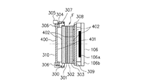
300は回転角0°の複屈折水晶板であり、被写界像を水平方向に2つに分離する(水平2点分離)。水晶の複屈折作用による点像分離幅は、切り出し角度45°の水晶厚み1mmにつき約5.87μであることから、必要な分離幅を得るためには、水晶の厚みをこの値に比例倍することによって容易に算出することができる。複屈折水晶板300が第一の光学部材を構成する。
301は赤外吸収フィルタであり、撮像素子106の分光感度と人間の視感度を概一致させる役目を持つ。302は水晶からなる偏光解消板(λ/4板)であり、複屈折水晶板300を通過することで直線偏光となった被写界光束の偏光解消を行い、再度円偏光に戻して射出する。赤外吸収フィルタ301と偏光解消板302とを貼り合わせて接合することで第二の光学部材を構成する。
303は回転角90°の複屈折水晶板であり、被写界像を上下方向に2つに分離する(上下2点分離)。複屈折水晶板303が第三の光学部材を構成する。複屈折水晶板303は、セラミックパッケージ106bに接着されることで撮像素子106の受光部(受光チップ)106aを保護する役目も果たす。
既述したように、複屈折水晶板300の上端部には振動素子305が接着固定される。振動素子305が複屈折水晶板300を振動させることにより、複屈折水晶板300の撮影レンズ105側の表面に付着する塵埃等の異物を除去することができる。振動素子305は、圧電体と内部電極とを交互に積層してなる積層型の圧電素子であり、積層方向により大きな振幅(変位)を発生するので、複屈折水晶板300を撮影光軸に直交する方向に大きく振動変位させることができる。
As described above, the
以上のように、第一の光学部材〜第三の光学部材により構成される光学フィルタFによってローパスフィルタ効果と赤外吸収(視感度補正)効果を持たせている。このように光学フィルタを3つの光学部材に分けることによって得られる利点は、異物除去のために振動を与える第一の光学部材(複屈折水晶板300)のみについて形状を含めて最適化することで、部材を効率良く振動を発生させることが可能となる点にある。さらに、図14で説明した光学フィルタの構成における撮像素子のカバーガラス309を光学フィルタの一部である第三の光学部材(複屈折水晶板303)で置き換えることでコストダウン可能となる点にある。
As described above, the low-pass filter effect and the infrared absorption (visibility correction) effect are provided by the optical filter F constituted by the first optical member to the third optical member. The advantage obtained by dividing the optical filter into three optical members in this way is that by optimizing only the first optical member (birefringent crystal plate 300) that gives vibration for removing foreign matters, including the shape. This is in that the member can efficiently generate vibration. Furthermore, the cost can be reduced by replacing the
次に、第一の光学部材〜第三の光学部材まわりの構成について説明する。307は第一の光学部材(複屈折水晶板300)と第二の光学部材(赤外吸収フィルタ301及び偏光解消板302の接合体)との間に配置された保持部材である。304は保持部材307と複屈折水晶板300との間に介在させた弾性部材であり、エラストマー(高分子物質)で形成されている。306はバネ性を有する金属板からなる押圧部材であり、複屈折水晶板300を弾性部材304に押圧することにより、複屈折水晶板300が保持部材307に対し浮遊保持される。これにより、圧電素子305の伸縮に追従した複屈折水晶板300の振動が許容されるとともに、振動により複屈折水晶板300が傷つくことが防止される。また、同時に複屈折水晶板300は、周囲四辺の近傍で、保持部材307に対して弾性部材304を介して隙間がないように密閉される。308は粘着シートであり、第一の光学部材及び第二の光学部材で構成されるフィルタユニット部と第三の光学部材(複屈折水晶板303)との間に異物が入り込まないように両者を密着固定する。
Next, the configuration around the first optical member to the third optical member will be described.
以上の構成より、光学フィルタFを、その有効光学範囲を密封空間に配置することができ、一度フィルタユニットの組立がなされれば、外部からの異物進入は阻止されることとなる。 With the above configuration, the effective optical range of the optical filter F can be arranged in a sealed space, and once the filter unit is assembled, entry of foreign matter from the outside is prevented.
ここで、第一の光学部材(複屈折水晶板300)の撮影レンズ105側の面には、導電性を有する反射防止多層膜である反射防止コート(ARコート)400が蒸着されている。ARコート400は、フッ素を含む材料からなる異物付着防止膜を最表層(最表面)としたものとなっている。また、第一の光学部材(複屈折水晶板300)の撮像素子106側の面には、撮影画像の色再現性を向上させるために、赤外光及び紫外光カット効果を有するダイクロイック多層膜であるUV−IRカットコート401が蒸着されている。
Here, on the surface of the first optical member (birefringent crystal plate 300) on the photographing
第二の光学部材(赤外吸収フィルタ301及び偏光解消板302の接合体)の両面、さらには撮像素子106に接着されている第三の光学部材(複屈折水晶板303)の両面には、通常の反射防止コート(ARコート)402が施されている。
On both surfaces of the second optical member (a joined body of the
フッ素を含む材料からなる異物付着防止膜の下層を、通常のUV−IRカットコートではなく、ARコート400にして、光学フィルタFの撮影レンズ105側の面に配置した理由は二つある。
There are two reasons why the lower layer of the foreign matter adhesion preventing film made of a material containing fluorine is not an ordinary UV-IR cut coat but an
一つ目の理由は、ARコート400の層数がUV−IRカットコートの層数に比べて一桁少ないので、フッ素材料と反射防止用材料の蒸着を行った際、蒸着物質が対象物以外に飛び散った微小粒子、いわゆるゴミ発生が少なくなるからである。すなわち、蒸着釜内部の清掃を行う回数を、フッ素材料とUV−IRカット用材料の蒸着組み合わせの場合に比べて、数分の一に減らすことが可能であり、これら工程負荷の改善によって光学フィルタのコストダウンに寄与することになる。
The first reason is that the number of layers of
二つ目の理由は、UV−IRカットコート401を光学フィルタの撮影レンズ105側の面に配置しないので、UV−IRカットコート401が静電気を帯びても、光学フィルタFの最前面の異物付着には直接関係がなくなるからである。これにより、通常の真空蒸着よりも信頼性、及び光学性能面で優っているイオンアシスト法にてUV−IRカットコート401の蒸着を行うことが可能となる。
The second reason is that the UV-
ここで、さらに図5を参照して、第一の光学部材(複屈折水晶板300)の表面に成膜された異物付着防止膜を有するARコート400、UV−IRカットコート401について説明する。図5は、複屈折水晶板300の厚み方向の様子を模式的に拡大した図である。実際には、複屈折水晶板300の厚みは1mm弱、蒸着層の蒸着物質であるSiO2、TiO2の一層あたりの厚みは100nm程度である。
Here, with reference to FIG. 5, the
まず、異物付着防止膜を有するARコート400について説明する。複屈折水晶板300の撮影レンズ105側の面には、真空蒸着にて、SiO2とびTiO2を交互に積層した5層のARコート400が成膜されており、その最表層には異物付着防止膜400aが成膜されている。
First, the
異物付着防止膜400aについて説明すると、異物の付着防止には、フッ素原子を含んだ物質を基材表面にコートすることが有効である。フッ素原子は原子半径及び分極率が小さいため、電気陰性度は元素の中で最も高い。また、炭素とフッ素の結合構成は、その結合エネルギーが非常に大きいため、耐熱性、耐光性に優れ、さらには分極率が小さいことから分子間凝集力が小さくなり、表面自由エネルギーを低くすることができる。表面自由エネルギーには、ファンデルワールス力に起因する分散項成分、クーロン静電力に関する極性項成分、水素結合力に基づく項、そのほか金属結合力等の分子間力が関係している。塵埃等の異物の付着防止には、該表面自由エネルギーが小さくなるフッ素系の材料をコートすることが有効である。
The foreign matter
フッ素系の材料には、炭化水素基の水素をフッ素に置き換えた、いわゆるパーフルオロアルキル基を含有する化合物、例えばパーフルオロアルキルシラン等が望ましい。また、特許文献4に記載されているように、フッ素化合物の一種であり、一般的な蒸着材料でもあるMgF2を表面コートすることも、フッ素系樹脂コートほどの効果までは及ばないが、やはり異物付着防止に適している。 As the fluorine-based material, a compound containing a so-called perfluoroalkyl group in which hydrogen of a hydrocarbon group is replaced with fluorine, for example, perfluoroalkylsilane is desirable. Further, as described in Patent Document 4, surface coating with MgF 2 , which is a kind of fluorine compound and also a general vapor deposition material, is not as effective as the fluorine resin coating, Suitable for preventing foreign matter adhesion.
しかしながら、単に基板表面にこれら異物付着防止膜400aを成膜すれば、異物の付着を充分に防げるという訳ではなく、異物付着防止膜400aの下層の膜、本実施形態ではARコート層が帯電していれば、静電気力による異物の付着が発生し易くなる。以下、この異物付着防止膜400aの下層の膜であるARコート層について説明する。
However, simply depositing the foreign matter
図5のARコート層を構成するSiO2とTiO2は、最も一般的に行われている通常の真空蒸着法にて蒸着がなされている。これらの蒸着物質は真空蒸着法にて蒸着がなされると、その蒸着層はポーラス状になる。この様子を図6の上図に示す。図6は、水晶基板の上に蒸着したUV−IR多層膜コートの断面をSEM(走査型電子顕微鏡)で撮影した写真である。図6の上図に示すように、とりわけTiO2がポーラス状に成膜されていることが分かる。一方、図6の下図はSiO2とTa2O5の蒸着物質を真空蒸着の一種であるイオンアシスト法(IAD)で成膜したUV−IR多層膜コートの断面写真である。上記通常の真空蒸着法のコートに対してSiO2とTa2O5が緻密な膜として成膜されていることがわかる。 The SiO 2 and TiO 2 constituting the AR coating layer in FIG. 5 are deposited by the usual vacuum deposition method that is most commonly performed. When these vapor deposition materials are vapor-deposited by a vacuum vapor deposition method, the vapor deposition layer becomes porous. This is shown in the upper diagram of FIG. FIG. 6 is a photograph of a cross section of the UV-IR multilayer coating deposited on the quartz substrate taken with a SEM (scanning electron microscope). As shown in the upper diagram of FIG. 6, it can be seen that TiO 2 is particularly formed in a porous form. On the other hand, the lower part of FIG. 6 is a cross-sectional photograph of a UV-IR multilayer coating in which SiO 2 and Ta 2 O 5 deposition materials are formed by an ion assist method (IAD) which is a kind of vacuum deposition. It can be seen that SiO 2 and Ta 2 O 5 is deposited as a dense film with respect to the normal vacuum evaporation coating.
イオンアシスト法は、真空蒸着中に数百eVのガスイオンを基板に照射して行われるもので、緻密な蒸着膜を成膜することができる。これに対して、通常の真空蒸着法では、成膜されたポーラス状層は密度が低く、吸水性を持ち、水分を含むことで蒸着層の屈折率変化、ひいてはコーティングの分光特性の変化を引き起こすことが一般的知られている。また、一方では、これらポーラス状層はその内部に水分を吸着することで蒸着層自体の電気抵抗が変化することが考えられる。 The ion assist method is performed by irradiating a substrate with gas ions of several hundred eV during vacuum deposition, and can form a dense deposited film. On the other hand, in a normal vacuum deposition method, the deposited porous layer has a low density, has water absorption, and moisture content causes a change in the refractive index of the deposited layer, and thus a change in the spectral characteristics of the coating. It is generally known. On the other hand, it is considered that the electrical resistance of the vapor deposition layer itself is changed by adsorbing moisture in the porous layer.
本出願人は、複屈折水晶板300の蒸着面を強制的に帯電させて、蒸着表面をGNDレベルに導電線にて接地させたとき、蒸着表面に電荷が残るか否か(0Vになるか否か)を測定するという実験を行った。図7に、本実験の概要を示す。図7において複屈折水晶板300の蒸着面に電荷を与えるのは帯電直流装置であり、帯電バーを水晶板に近接させることで容易に電荷を帯びさせることができる。次に、複屈折水晶板300の蒸着面に表面電位計のプローブを近づけ、蒸着面が500V以上帯電していることを確認した後、蒸着面をGNDレベルに導電線にて接地させる。このときに蒸着表面に電荷が残るか否か(0Vになるか否か)を表面電位計で再度測定するという実験を行うことで、複屈折水晶板300の蒸着面の電荷抜けの判定を行った。
Applicant has forcibly charged the vapor deposition surface of the
表1が実験の結果である。試料はすべて水晶板に各種コートを施してある。UV−IR1は、SiO2を最表面にして以下水晶基板に向かってTiO2、SiO2を交互に各膜厚100nm前後で40層積層させた一般的なUV−IRカットコートである。UV−IR1は、通常の真空蒸着法で成膜されたものである。また、UV−IR2は、SiO2を最表層にして以下水晶基板に向かってTa2O5、SiO2を交互に各膜厚100nm前後で40層積層させたUV−IR1と同分光仕様のUV−IRカットコートである。UV−IR2は、イオンアシスト法で成膜されたものである。これらコートについて上記帯電実験を行ったところ、通常真空蒸着で成膜されたUV−IR1コートでは、導電線の接地により電荷が抜けて蒸着表面が0Vに落ちることが確認できた。しかしながら、イオンアシスト法で成膜されたUV−IR2コートでは、ほとんど電荷の変化がなく、電荷除去が行われなかった。 Table 1 shows the results of the experiment. All samples have various coatings on the quartz plate. UV-IR1 is a general UV-IR cut coat in which 40 layers of TiO 2 and SiO 2 are alternately laminated with a thickness of around 100 nm toward the quartz substrate with SiO 2 as the outermost surface. UV-IR1 is formed by a normal vacuum deposition method. UV-IR2 has the same spectroscopic specification as UV-IR1 in which 40 layers of Ta 2 O 5 and SiO 2 are alternately laminated with a thickness of about 100 nm toward the quartz substrate with SiO 2 as the outermost layer. -IR cut coat. UV-IR2 is formed by an ion assist method. As a result of conducting the above charging experiment on these coats, it was confirmed that in the UV-IR1 coat, which was usually formed by vacuum deposition, the charge was released by the grounding of the conductive wire and the deposition surface dropped to 0V. However, in the UV-IR2 coat formed by the ion assist method, there was almost no change in charge, and charge removal was not performed.
また、AR1は、SiO2を最表層にして以下ZrO2、Al2O3の3層からなる一般的な反射防止コートである。AR1コートについて上記帯電実験を行ったところ、電荷除去が行われなかった。 AR1 is a general antireflection coating composed of three layers of ZrO 2 and Al 2 O 3 with SiO 2 as the outermost layer. When the above charging experiment was performed on the AR1 coat, charge removal was not performed.
また、AR2は、UV−IR1と同様な膜構成であるSiO2を表面にして水晶基板に向かってTiO2、SiO2を交互に各膜厚100nm前後で5層に積層させ、さらに表面のSiO2の上に100nm程度のMgF2を異物付着防止膜として最表層に成膜したARコートである。AR2コートについて上記帯電実験を行ったところ、電荷除去が確認できた。また、AR2コートのMgF2の代わりに異物付着防止膜として最表層にフッ素系材料を10nm程度に成膜したAR3コートについて上記帯電実験を行ったところ、電荷除去が確認できた。 In addition, AR2 has a film structure similar to that of UV-IR1, with SiO 2 as the surface, and TiO 2 and SiO 2 are alternately laminated in five layers with a film thickness of about 100 nm toward the quartz substrate. In this AR coating, MgF 2 having a thickness of about 100 nm is formed on the outermost layer as a foreign matter adhesion preventing film. When the above charging experiment was performed on the AR2 coat, charge removal was confirmed. In addition, when the above charging experiment was performed on the AR3 coat in which a fluorine-based material was formed on the outermost layer as a foreign matter adhesion prevention film instead of the AR2 coat MgF 2 , the charge removal was confirmed.

以上のことから、水晶基板上に通常真空蒸着にてSiO2、TiO2を交互に成膜することによってできたTiO2のポーラス状膜組織を有するコートは、その蒸着表面を接地すれば電荷除去が可能であることが分かった。さらには、その表面のSiO2上に異物付着防止膜としてコートしたフッ素を含む高分子材料、或いはMgF2(フッ化マグネシウム)の層は、除電を行う上で障害とならないことがわかった。 From the above, a coat having a porous film structure of TiO 2 formed by alternately depositing SiO 2 and TiO 2 on a quartz substrate by normal vacuum deposition removes the charge if the deposition surface is grounded. Was found to be possible. Furthermore, it has been found that a fluorine-containing polymer material or MgF 2 (magnesium fluoride) layer coated on SiO 2 on the surface as a foreign matter adhesion preventing film does not become an obstacle to static elimination.
そこで、本実施形態では、複屈折水晶板300に異物が付着するのを防止するために、複屈折水晶板300に対し、蒸着層の蒸着物質であるSiO2、TiO2を交互に真空蒸着で成膜し、その最表層に異物付着防止膜400aを成膜した構成をとる。これにより、静電気力を発生しない、表面自由エネルギーの低い、つまり異物付着の少ないARコート400を配することが可能となっている。
Therefore, in this embodiment, in order to prevent foreign matter from adhering to the
次に、UV−IRカットコート401について説明を行う。UV−IRカットコート401を行う目的は、赤外吸収フィルタ301のみでは撮像素子の分光感度を視感度に一致するようにはできないために、特定の波長領域をカットすることにある。具体的には、次の3つの波長領域のカット効果を持たせている。すなわち、撮影レンズ105の青色のにじみを改善するために、400nm近傍をカットする。赤外吸収フィルタ301が赤色700nm近傍で緩やかな吸収、減光をするのをシャープにカットする。1000nmを超えた赤外領域にて赤外吸収フィルタ301の透過率が徐々に高くなるのをカットする。
Next, the UV-
UV−IRカットコート401は、図5に示すように、SiO2を最表層にして、以下水晶基板に向かってTiO2、SiO2を交互に各膜厚100nm前後真空蒸着にて40層程度積層したものである。或いは、SiO2を最表層にして、以下水晶基板に向かってTa2O5、SiO2をイオンアシスト法で40層程度積層させたものでも良い。
As shown in FIG. 5, the UV-
上述したように、ARコート400が、赤外吸収フィルタ301を含む光学フィルタFの最前面に配置され、異物付着を防止するための帯電防止効果が要求される。それに対して、UV−IRカットコート401は、光学フィルタF内部に配置されることになるため、帯電を気にする必要はない。したがって、より緻密で強度が強く、分光特性の変化がほとんどない膜を成膜することのできるイオンアシスト法にて蒸着することが可能となり、分光特性上、環境信頼性上も大きな利点となる。
As described above, the
なお、図4では、UV−IRカットコート401を複屈折水晶板300の裏面(撮像素子106側の面)に配置しているが、その裏面と対向する面である赤外吸収フィルタ301の撮影レンズ105側の面に配置しても良い。
In FIG. 4, the UV-
また、第二の光学部材において、赤外吸収フィルタ301と偏光解消板302を反転して(前後逆に)配置してもその作用は全く同じである。反転させた場合は、やはり複屈折水晶板300の裏面と対向する面である偏光解消板302の撮影レンズ105側の面にUV−IRカットコート401を配置する。
In the second optical member, even if the
すなわち、UV−IRカットコート401は、第一の光学部材の裏面(撮像素子106側の面)、又は、第二の光学部材の撮影レンズ105側の面に成膜することとする。この理由を図8、図9を用いて説明する。
That is, the UV-
図8は、図4から光学要素のみを抜き出した図であり、光学要素の配置及びその表面に施されたコートは図4で説明した通りである。また、図9は、UV−IRカットコート401の分光透過率、赤外吸収フィルタ301の透過率、さらにこの2つの透過率をかけ合わせた総合の透過率を示す特性図である。撮像素子106に入射する被写界光の分光は、この総合透過率で決定される。同図から分かるように、UV−IRカットコート401の赤外側の透過率は、670nm近傍で50%透過率になるように設計がなされており、逆に言うと670nmから赤外領域においては50%以上の高い反射率となっている。一方では、400nm〜670nmの間の反射率は2%以内に抑えられている。
FIG. 8 is a diagram in which only the optical element is extracted from FIG. 4, and the arrangement of the optical element and the coating applied to the surface thereof are as described in FIG. FIG. 9 is a characteristic diagram showing the spectral transmittance of the UV-
図8に説明を戻し、被写界に配置したスポット光が、撮像のゴースト光としてどのように撮像素子106に入射するか(撮像されるか)について説明する。撮影レンズ105から入射した被写界のスポット光は、複屈折水晶板300、赤外吸収フィルタ301及び偏光解消板302を通り、さらには複屈折水晶板303を透過して、撮像素子106の受光部106aに入射する。通常、ARコート400、402は、400nm〜700nmの可視域においておおよそ1%以下の反射率であるが、受光部106aの反射率は広帯域に渡って約6%と比較的高い。そのため、受光部106a表面のA1点において反射光束が発生する。ここで反射した光束は再度光学フィルタFに戻ることになるが、光学フィルタFの中で可視域における反射率の高いのは、上述したように可視域670nm〜700nmにおいて50%以上あるUV−IRカットコート401である。したがって、A1点で反射したスポット光束はA2点にて再度反射され、撮像素子106の受光部106a表面のA3点に再入射する。結果として、撮像された画像は焦点の合った被写体であるスポット光と近接してA1−A3を略直径としたピントのずれたゴースト光が発生することになる。
Returning to FIG. 8, description will be given of how the spot light arranged in the object field enters the
ただし、A1点で反射したスポット光束は最終的にA3点に至るまでに、赤外吸収フィルタ301をさらに2回透過することになる。670nm〜700nmにおける赤外吸収フィルタ301の透過率は10%強であることから、670nm〜700nm波長において、受光部106a表面のA3点の反射率を6%、UV−IRカットコート401の平均反射率を75%としても、6%×0.75×0.1×0.1=0.045%の強度にまで減衰してしまう。一方、ARコートされた媒質各界面での反射も撮像素子106にゴースト光として入射するが、これらの強度は400nm〜700nmの可視域において、ARコート400の反射率は約1%であることから、6%×0.01=0.06%となる。これが界面の数、計5面で発生する。したがって、以上のゴースト光が重なり合ったとしても、400nm〜700nmの可視域波長において平坦な分光で、かつ直接光強度の0.3〜0.4%程度の違和感のないゴースト光として撮像がなされることになる。
However, the spot light beam reflected at the point A1 finally passes through the
本実施形態では、UV−IRカットコート401の蒸着面を複屈折水晶板300の裏面に配置しているが、赤外吸収フィルタ301の表面(撮影レンズ105側の面)に設けるようにしてもよい。この場合、ゴーストの大きさはやや小さくなり、強度は若干強くなるという違いはあるが、ほぼ同様のゴーストが撮像されることとなる。
In this embodiment, the vapor deposition surface of the UV-
一方、UV−IRカットコート401を赤外吸収フィルタ301よりも撮像素子106側に配した場合のゴースト強度について説明する。例えば偏光解消板302の撮像素子106側に面にUV−IRカットコート401を成膜した場合を想定して上記同様ゴースト光強度について考えてみる。図8において、受光部106aの表面のA1点において発生した6%の反射光束は、偏光解消板302の表面で670nm〜700nmにおいて平均75%の高い反射率で反射し、この反射光束はそのまま受光部106aに入射してしまう。この反射率を上記同様670nm〜700nm波長において計算すると、6%×0.75=4.5%の強い強度となる。他の界面での反射率は上記同様0.06%が5面で発生することから、ゴーストの重なり強度としても可視域400nm〜700nm全体で約5%、そのうち670nm〜700nm波長の強度が約90%を占めることになる。その結果、撮像された画像は焦点の合った被写体であるスポット光と近接してA1−B2を略直径とし、上記例よりも大きさは小さいが非常に強度の強い赤いゴースト光が発生することになり、画像の品位を著しく低下させることになってしまう。
On the other hand, the ghost intensity when the UV-
したがって、赤外吸収フィルタ301よりも撮影レンズ105側にUV−IRカットコート401を配置することは、ゴースト光を目立たなくするために画像品位上重要となる。
Therefore, disposing the UV-
(第2の実施の形態)
次に、図10を参照して、本発明の第2の実施形態を説明する。図10は、光学フィルタF及び撮像素子106まわりの断面拡大図であり、第1の実施形態における図4に相当する。なお、図4に示した構成要素と同一のものには同一の符号を付して説明する。
(Second Embodiment)
Next, a second embodiment of the present invention will be described with reference to FIG. FIG. 10 is an enlarged cross-sectional view around the optical filter F and the
第1の実施形態との相違点は、第二の光学部材が、第1の実施形態では赤外吸収フィルタ301及び偏光解消板302の接合体であったのに対して、さらに回転角90°の複屈折水晶板303が追加されており、計3つの光学要素が貼り合わされた構成となっていることにある。
The difference from the first embodiment is that the second optical member is a joined body of the
第一の光学部材(複屈折水晶板300)の撮影レンズ105側の面には、異物付着防止膜を最表層としたARコート400が蒸着されており、裏面には、UV−IRカットコート401が蒸着されている点は第1の実施形態と同じである。ただし、ローパス効果はこの第一の光学要素と第二の光学要素で完結するので、撮像素子106の受光部106aを保護する役目はカバーガラス(保護ガラス)309となっている。もちろん、第1の実施形同様、UV−IRカットコート401が成膜される面は、複屈折水晶板300の裏面ではなく、第二の光学要素の撮影レンズ105側の面であっても良い。
An
第2の実施形態では、撮像素子106にカバーガラス309を使用するという極一般的な撮像素子を使用できることから、撮像素子を製造するメーカの選択自由度が増え、撮像素子の供給、コスト上有利となる。これは、第1の実施形態の構成である複屈折水晶板303をセラミックパッケージ106bに高い信頼性を持って貼り付けられた撮像素子を作るためには、セラミックパッケージ106bの材料の線膨張率を極力、水晶のものに近づけるという技術等が必要となるためである。
In the second embodiment, since a very general image pickup device using the
(第3の実施の形態)
次に、図11を参照して、本発明の第3の実施形態を説明する。図11は、光学フィルタF及び撮像素子106まわりの断面拡大図であり、第1の実施形態における図4に相当する。なお、図4に示した構成要素と同一のものには同一の符号を付して説明する。
(Third embodiment)
Next, a third embodiment of the present invention will be described with reference to FIG. FIG. 11 is an enlarged cross-sectional view around the optical filter F and the
第1の実施形態との相違点は、第二の光学部材が赤外吸収フィルタ301のみになっていることにある。
The difference from the first embodiment is that the second optical member is only the
第一の光学部材(複屈折水晶板300)の撮影レンズ105側の面には、異物付着防止膜を最表層としたARコート400が蒸着されており、裏面には、UV−IRカットコート401が蒸着されている点は第1の実施形態と同じである。また、第2の実施形態と同様、撮像素子106の保護はカバーガラス309で行っている。
An
第3の実施形態では、複屈折水晶板が1枚のみであり、水平方向2点点像分離しかしないため、垂直方向のローパス効果はなく偽色が発生する確率は高くなるが、水晶板を2枚削減できるので、低コストタイプのカメラに適している。もちろん、複屈折水晶板には回転角0°の代わりに90°のものを使用しても良い。 In the third embodiment, since there is only one birefringent quartz plate and only two point images are separated in the horizontal direction, there is no low-pass effect in the vertical direction and the probability of generating false colors is high. Since it can reduce the number of images, it is suitable for low-cost cameras. Of course, a birefringent quartz plate having a rotation angle of 90 ° instead of 0 ° may be used.
(第4の実施の形態)
次に、図12を参照して、本発明の第4の実施形態を説明する。図12は、光学フィルタF及び撮像素子106まわりの断面拡大図であり、第1の実施形態における図4に相当する。なお、図4に示した構成要素と同一のものには同一の符号を付して説明する。
(Fourth embodiment)
Next, a fourth embodiment of the present invention will be described with reference to FIG. FIG. 12 is an enlarged cross-sectional view around the optical filter F and the
第1の実施形態との相違点は、第3の実施形態と同様、第二の光学部材が赤外吸収フィルタ301のみになっていることにある。そして、赤外吸収フィルタ301が撮像素子106に接着されることで、撮像素子106の受光チップ106aを保護する役目を兼ねている。
The difference from the first embodiment is that the second optical member is only the
第一の光学部材(複屈折水晶板300)の撮影レンズ105側の面には、異物付着防止膜を最表層としたARコート400が蒸着されており、裏面には、UV−IRカットコート401が蒸着されている点は第1の実施形態と同じである。
An
第4の実施形態でも、上述した第3の実施形態と同様、水平2点点像分離タイプであるが、さらにカバーガラス309が不要となるため、さらなるコストダウンが可能である。ただし、セラミックパッケージ106b材料の線膨張係数を、UV−IRカットコート401の線膨張係数に近い材料に設定する必要がある。
The fourth embodiment is also a horizontal two-point image separation type as in the third embodiment described above. However, since the
(第5の実施の形態)
次に、図13を参照して、本発明の第5の実施形態を説明する。図13は、光学フィルタF及び撮像素子106まわりの断面拡大図であり、第1の実施形態における図4に相当する。なお、図4に示した構成要素と同一のものには同一の符号を付して説明する。
(Fifth embodiment)
Next, a fifth embodiment of the present invention will be described with reference to FIG. FIG. 13 is an enlarged cross-sectional view around the optical filter F and the
本実施形態では、図14でも説明した4枚貼り合せ構造の光学フィルタそのもの(回転角0°の複屈折水晶板300、赤外吸収フィルタ301、偏光解消板302、回転角90°の複屈折水晶板303)を第二の光学部材とした構造となっている。この4枚貼り合せの光学フィルタの最前面が、通常の反射防止コート402になっている。
In the present embodiment, the optical filter having the four-layer structure described with reference to FIG. 14 itself (
一方、S−BSL7なる光学的特性の良いガラス板310が第一の光学部材を構成する。第一の光学部材(ガラス板310)の撮影レンズ105側の面には、異物付着防止膜を最表層としたARコート400が蒸着されており、裏面には、UV−IRカットコート401が蒸着されている点は第1の実施形態と同じである。また、本実施形態では、ガラス板310がその撮影レンズ105側の表面に付着した異物を振動によって除去するための振動対象物になっている。
On the other hand, a
第5の実施形態では、異物除去のための振動発生の最適化を行う上で、従来の光学ローパスフィルタと赤外吸収フィルタからなる光学フィルタFはそのままに、振動対象であるガラス板310についてのみ、その材質、厚み、形状、さらには振動素子の駆動電圧、駆動波形といった振動を発生する上に決定すべきパラメータを最適化すれば良い。そして、一旦振動の最適化がなされれば、光学フィルタFの仕様が変更されても、振動メカニズムを変更する必要がないという利点がある。
In the fifth embodiment, in optimizing the generation of vibration for removing foreign matters, the optical filter F composed of the conventional optical low-pass filter and infrared absorption filter is left as it is, and only the
F 光学フィルタ
101 CPU
105 撮影レンズ
106 撮像素子
106a 受光部
300 複屈折水晶板(回転角90°)
301 赤外吸収フィルタ
302 偏光解消板
303 複屈折水晶板(回転角90°)
310 ガラス板
400 反射防止コート
401 UV−IRカットコート
402 反射防止コート
105
301 Infrared Absorption Filter 302
310
Claims (10)
前記光学フィルタは、第一の光学部材と、前記第一の光学部材よりも前記撮像素子側に配置され、赤外成分を吸収する第二の光学部材と、前記第一の光学部材の入射面を露出させるとともに、前記第一の光学部材の射出面と前記第二の光学部材の入射面までの間に密閉空間が形成されるように前記第一の光学部材と前記第二の光学部材とを保持する保持部材とを備え、
前記第一の光学部材の入射面に導電性を有する反射防止多層膜を成膜し、前記密閉空間内となる面に、赤外光及び紫外光を遮断するダイクロイック多層膜を成膜し、前記反射防止多層膜の層数は前記ダイクロイック多層膜の層数よりも少なく構成され、前記反射防止多層膜の最表層にフッ素を含む材料からなる膜を成膜し、前記反射防止多層膜は、ポーラス状に成膜されたSiO 2 及びTiO 2 から構成されることを特徴とする光学フィルタ。 An optical filter disposed in front of the image sensor,
The optical filter includes a first optical member, a second optical member that is disposed closer to the imaging element than the first optical member, and absorbs an infrared component, and an incident surface of the first optical member The first optical member and the second optical member so that a sealed space is formed between the exit surface of the first optical member and the incident surface of the second optical member. A holding member for holding
An antireflection multilayer film having conductivity is formed on the incident surface of the first optical member, and a dichroic multilayer film that blocks infrared light and ultraviolet light is formed on the surface that is in the sealed space, The number of layers of the antireflection multilayer film is less than the number of layers of the dichroic multilayer film, and a film made of a material containing fluorine is formed on the outermost layer of the antireflection multilayer film. an optical filter, characterized in Rukoto consists SiO 2 and from TiO 2 which is formed on Jo.
前記光学フィルタは、前記撮像素子の前に配置される第一の光学部材と、前記第一の光学部材よりも撮像素子側に配置され、赤外成分を吸収する第二の光学部材と、前記第一の光学部材の入射面を露出させるとともに、前記第一の光学部材の射出面と前記第二の光学部材の入射面までの間に密閉空間が形成されるように前記第一の光学部材と前記第二の光学部材とを保持する保持部材とを備え、
前記第一の光学部材の入射面に導電性を有する反射防止多層膜を成膜し、前記密閉空間内となる面に、赤外光及び紫外光を遮断するダイクロイック多層膜を成膜し、前記反射防止多層膜の層数は前記ダイクロイック多層膜の層数よりも少なく構成され、前記反射防止多層膜の最表層にフッ素を含む材料からなる膜を成膜し、前記反射防止多層膜は、ポーラス状に成膜されたSiO 2 及びTiO 2 から構成されることを特徴とする撮像装置。 An imaging device comprising an imaging element and an optical filter disposed in front of the imaging element,
The optical filter includes a first optical member disposed in front of the image sensor, a second optical member that is disposed closer to the image sensor than the first optical member, and absorbs an infrared component; The first optical member is exposed such that an incident surface of the first optical member is exposed and a sealed space is formed between the exit surface of the first optical member and the incident surface of the second optical member. And a holding member for holding the second optical member,
An antireflection multilayer film having conductivity is formed on the incident surface of the first optical member, and a dichroic multilayer film that blocks infrared light and ultraviolet light is formed on the surface that is in the sealed space, The number of layers of the antireflection multilayer film is less than the number of layers of the dichroic multilayer film, and a film made of a material containing fluorine is formed on the outermost layer of the antireflection multilayer film. Jo consists the formed SiO 2 and TiO 2 in the imaging apparatus according to claim Rukoto.
Priority Applications (3)
| Application Number | Priority Date | Filing Date | Title |
|---|---|---|---|
| JP2008149637A JP5268436B2 (en) | 2008-06-06 | 2008-06-06 | Optical filter and imaging device |
| CN200910142384XA CN101598828B (en) | 2008-06-06 | 2009-06-04 | Optical filter and imaging apparatus |
| US12/478,269 US20090303590A1 (en) | 2008-06-06 | 2009-06-04 | Optical filter and imaging apparatus |
Applications Claiming Priority (1)
| Application Number | Priority Date | Filing Date | Title |
|---|---|---|---|
| JP2008149637A JP5268436B2 (en) | 2008-06-06 | 2008-06-06 | Optical filter and imaging device |
Related Child Applications (1)
| Application Number | Title | Priority Date | Filing Date |
|---|---|---|---|
| JP2013054967A Division JP5677491B2 (en) | 2013-03-18 | 2013-03-18 | Optical filter and imaging device |
Publications (3)
| Publication Number | Publication Date |
|---|---|
| JP2009294532A JP2009294532A (en) | 2009-12-17 |
| JP2009294532A5 JP2009294532A5 (en) | 2011-07-21 |
| JP5268436B2 true JP5268436B2 (en) | 2013-08-21 |
Family
ID=41400062
Family Applications (1)
| Application Number | Title | Priority Date | Filing Date |
|---|---|---|---|
| JP2008149637A Expired - Fee Related JP5268436B2 (en) | 2008-06-06 | 2008-06-06 | Optical filter and imaging device |
Country Status (3)
| Country | Link |
|---|---|
| US (1) | US20090303590A1 (en) |
| JP (1) | JP5268436B2 (en) |
| CN (1) | CN101598828B (en) |
Families Citing this family (13)
| Publication number | Priority date | Publication date | Assignee | Title |
|---|---|---|---|---|
| WO2011158635A1 (en) | 2010-06-18 | 2011-12-22 | 株式会社大真空 | Infrared blocking filter |
| JP5703825B2 (en) * | 2011-02-22 | 2015-04-22 | ソニー株式会社 | Imaging device and camera module |
| JP5765052B2 (en) * | 2011-05-13 | 2015-08-19 | 旭硝子株式会社 | Optical components and optical devices |
| JP2013033225A (en) | 2011-06-30 | 2013-02-14 | Canon Inc | Imaging apparatus and image forming apparatus |
| CN102759768B (en) * | 2012-07-31 | 2014-12-31 | 杭州科汀光学技术有限公司 | Optical filter |
| DE102015114877B4 (en) * | 2015-09-04 | 2020-10-01 | Schott Ag | Scratch-resistant anti-reflective coating and mobile electronic device |
| CN106054299B (en) * | 2016-07-29 | 2019-05-28 | 利达光电股份有限公司 | A kind of cutoff filter and its film plating process of easy cleaning |
| CN107870379A (en) * | 2016-11-04 | 2018-04-03 | 江苏日久光电股份有限公司 | Display screen screen sticking film |
| CN106814411A (en) * | 2017-02-22 | 2017-06-09 | 深圳市保千里电子有限公司 | A kind of eyeglass of mobile phone full shot, full shot and imaging method |
| KR102426728B1 (en) * | 2017-04-10 | 2022-07-29 | 삼성전자주식회사 | Method and electronic device for focus control |
| US11231533B2 (en) * | 2018-07-12 | 2022-01-25 | Visera Technologies Company Limited | Optical element having dielectric layers formed by ion-assisted deposition and method for fabricating the same |
| US11314004B2 (en) | 2019-04-08 | 2022-04-26 | Visera Technologies Company Limited | Optical filters and methods for forming the same |
| CN111443418B (en) * | 2020-05-12 | 2022-04-08 | 苏州江泓电子科技有限公司 | Polarizing multilayer film for vacuum ultraviolet band of 70-100 nm and preparation method thereof |
Family Cites Families (18)
| Publication number | Priority date | Publication date | Assignee | Title |
|---|---|---|---|---|
| US3561934A (en) * | 1967-09-11 | 1971-02-09 | Crucible Inc | Sintered steel particles containing dispersed carbides |
| JPH0763056B2 (en) * | 1986-08-06 | 1995-07-05 | 三菱電機株式会社 | Thin film forming equipment |
| JPH03261047A (en) * | 1990-03-09 | 1991-11-20 | Toshiba Corp | Display unit |
| WO1996017498A1 (en) * | 1994-11-30 | 1996-06-06 | Philips Electronics N.V. | Imaging device with anti-condensation provision |
| US6287683B1 (en) * | 1997-04-09 | 2001-09-11 | Canon Kabushiki Kaisha | Anti-fogging coating and optical part using the same |
| US6280848B1 (en) * | 1998-10-06 | 2001-08-28 | Minolta Co., Ltd. | Antireflection coating |
| JP3989296B2 (en) * | 2002-05-20 | 2007-10-10 | オリンパス株式会社 | Camera and image sensor unit |
| US6818962B2 (en) * | 2002-10-25 | 2004-11-16 | Omnivision International Holding Ltd | Image sensor having integrated thin film infrared filter |
| JP4426946B2 (en) * | 2004-10-27 | 2010-03-03 | オリンパス株式会社 | Digital camera system |
| JP4171362B2 (en) * | 2003-07-10 | 2008-10-22 | Agcテクノグラス株式会社 | Transparent substrate with antireflection film |
| JP2005148379A (en) * | 2003-11-14 | 2005-06-09 | Nikon Corp | Optical element and imaging device |
| JP2005308968A (en) * | 2004-04-20 | 2005-11-04 | Olympus Corp | Optical multilayer film and optical element |
| JP2006163275A (en) * | 2004-12-10 | 2006-06-22 | Kyocera Kinseki Corp | Optical component |
| TWI382280B (en) * | 2005-07-27 | 2013-01-11 | Shinetsu Chemical Co | Resist protective coating material and patterning process |
| JP4958536B2 (en) * | 2006-01-12 | 2012-06-20 | 富士フイルム株式会社 | Anti-reflection coating |
| JP4804251B2 (en) * | 2006-07-20 | 2011-11-02 | キヤノン株式会社 | Imaging device and imaging unit |
| TWI408404B (en) * | 2006-07-25 | 2013-09-11 | Pentax Ricoh Imaging Co Ltd | Imaging device |
| US20080258043A1 (en) * | 2007-04-17 | 2008-10-23 | Koji Suzuki | Optical element and optical equipment |
-
2008
- 2008-06-06 JP JP2008149637A patent/JP5268436B2/en not_active Expired - Fee Related
-
2009
- 2009-06-04 US US12/478,269 patent/US20090303590A1/en not_active Abandoned
- 2009-06-04 CN CN200910142384XA patent/CN101598828B/en not_active Expired - Fee Related
Also Published As
| Publication number | Publication date |
|---|---|
| CN101598828A (en) | 2009-12-09 |
| JP2009294532A (en) | 2009-12-17 |
| CN101598828B (en) | 2011-09-28 |
| US20090303590A1 (en) | 2009-12-10 |
Similar Documents
| Publication | Publication Date | Title |
|---|---|---|
| JP5268436B2 (en) | Optical filter and imaging device | |
| JP4462197B2 (en) | Optical low-pass filter | |
| US7903158B2 (en) | Image capturing apparatus with adhesion suppressing capabilities | |
| JP5121443B2 (en) | Imaging device and optical filter | |
| JP5280321B2 (en) | Camera body and imaging device | |
| US7476042B2 (en) | Image capture apparatus | |
| EP1650957B1 (en) | Optical device and control method thereof | |
| US20080018775A1 (en) | Image pickup apparatus and image pickup unit having device for removing foreign substance deposited on surface of optical member | |
| JP2010103921A (en) | Imaging apparatus and method for controlling the same | |
| US20080019686A1 (en) | Image pickup apparatus having device for removing foreign substance deposited on surface of optical member | |
| JP2001272708A (en) | Image pickup device for both of visible ray and ir ray | |
| JP2011175107A (en) | Optical device and optical apparatus | |
| JP5677491B2 (en) | Optical filter and imaging device | |
| JP2005148379A (en) | Optical element and imaging device | |
| US6965134B2 (en) | Image pick-up unit including an image pick-up device and optical filter layers | |
| JP5111219B2 (en) | Optical equipment | |
| JP4788384B2 (en) | Imaging device | |
| JP2015232669A (en) | Optical filter of imaging apparatus | |
| JP4795286B2 (en) | Imaging device | |
| JP2006243674A (en) | Optical element and optical equipment | |
| JP5018835B2 (en) | Imaging device, optical apparatus, and manufacturing method of imaging device | |
| JP2008244770A (en) | Manufacturing method of optical apparatus, optical element, and cover member | |
| JP2004297398A (en) | Imaging optical system and image pickup device using the same | |
| JP2006060712A (en) | Electronic camera | |
| JP2008042488A (en) | Image equipment and camera |
Legal Events
| Date | Code | Title | Description |
|---|---|---|---|
| A521 | Written amendment |
Free format text: JAPANESE INTERMEDIATE CODE: A523 Effective date: 20110603 |
|
| A621 | Written request for application examination |
Free format text: JAPANESE INTERMEDIATE CODE: A621 Effective date: 20110603 |
|
| A977 | Report on retrieval |
Free format text: JAPANESE INTERMEDIATE CODE: A971007 Effective date: 20120528 |
|
| A131 | Notification of reasons for refusal |
Free format text: JAPANESE INTERMEDIATE CODE: A131 Effective date: 20120605 |
|
| A521 | Written amendment |
Free format text: JAPANESE INTERMEDIATE CODE: A523 Effective date: 20120730 |
|
| A131 | Notification of reasons for refusal |
Free format text: JAPANESE INTERMEDIATE CODE: A131 Effective date: 20130115 |
|
| A521 | Written amendment |
Free format text: JAPANESE INTERMEDIATE CODE: A523 Effective date: 20130313 |
|
| TRDD | Decision of grant or rejection written | ||
| A01 | Written decision to grant a patent or to grant a registration (utility model) |
Free format text: JAPANESE INTERMEDIATE CODE: A01 Effective date: 20130409 |
|
| A61 | First payment of annual fees (during grant procedure) |
Free format text: JAPANESE INTERMEDIATE CODE: A61 Effective date: 20130507 |
|
| R151 | Written notification of patent or utility model registration |
Ref document number: 5268436 Country of ref document: JP Free format text: JAPANESE INTERMEDIATE CODE: R151 |
|
| LAPS | Cancellation because of no payment of annual fees |