JP5111219B2 - Optical equipment - Google Patents
Optical equipment Download PDFInfo
- Publication number
- JP5111219B2 JP5111219B2 JP2008111770A JP2008111770A JP5111219B2 JP 5111219 B2 JP5111219 B2 JP 5111219B2 JP 2008111770 A JP2008111770 A JP 2008111770A JP 2008111770 A JP2008111770 A JP 2008111770A JP 5111219 B2 JP5111219 B2 JP 5111219B2
- Authority
- JP
- Japan
- Prior art keywords
- conductive portion
- optical
- foreign matter
- optical member
- state
- Prior art date
- Legal status (The legal status is an assumption and is not a legal conclusion. Google has not performed a legal analysis and makes no representation as to the accuracy of the status listed.)
- Expired - Fee Related
Links
Images


Description
本発明は、デジタルカメラ等の光学機器に関する。 The present invention relates to an optical equipment such as a digital camera.
従来から、レンズ交換式デジタル一眼レフカメラの撮影レンズの焦点面近傍に塵埃等の異物が存在すると、その異物が影となって画像に写り込んでしまうという問題がある。このような異物が発生する原因としては、レンズ交換時に塵埃が外部から侵入したり、カメラ内部でのシャッタやミラーの動作に伴い、その構造部材である樹脂等の微細な磨耗紛が発生したりすることが考えられている。 Conventionally, when a foreign substance such as dust is present in the vicinity of the focal plane of the taking lens of the interchangeable lens type digital single-lens reflex camera, there is a problem that the foreign substance is reflected in an image as a shadow. The cause of such foreign matter is that dust enters from the outside during lens replacement, or fine wear powder such as resin, which is a structural member, is generated with the operation of the shutter and mirror inside the camera. It is considered to be.
上記のような原因で発生した異物が、特に固体撮像素子の保護用のカバーガラスとカバーガラスの前面に配設されている赤外カットフィルタや光学ローパスフィルタ等の光学フィルタとの間に入り込んでしまった場合には、その異物を除去するためにカメラを分解しなければならなかった。そのため、カバーガラスと光学フィルタとの間に異物が入り込まないように密閉構造にすることは極めて有効なものであった。 The foreign matter generated due to the above-mentioned causes has entered especially between the cover glass for protecting the solid-state imaging device and an optical filter such as an infrared cut filter or an optical low-pass filter disposed in front of the cover glass. If it did, the camera had to be disassembled to remove the foreign material. For this reason, it has been extremely effective to provide a sealed structure so that foreign matter does not enter between the cover glass and the optical filter.
しかしながら、光学フィルタのうち固体撮像素子との対向面と反対側の表面に異物が付着した場合、それが焦点面近傍である場合には、その異物が影となって画像に写り込んでしまうという問題が依然として残っている。 However, if a foreign object adheres to the surface of the optical filter opposite to the surface facing the solid-state imaging device, if the object is near the focal plane, the foreign object will appear as a shadow in the image. The problem remains.
上記のような問題を解決するために、固体撮像素子のカバーガラスの表面をワイパーや植毛紙で清掃するものが提案されている(例えば特許文献1及び特許文献2を参照)。また、光学フィルタ等の光学部材に振動を加えることで、その表面に付着した異物を除去するものが提案されている(例えば特許文献3を参照)。
In order to solve the above problems, there has been proposed a method of cleaning the surface of a cover glass of a solid-state imaging device with a wiper or a flocked paper (for example, see
ところで、カメラが置かれる環境によっては、カバーガラスや光学フィルタの表面に結露が発生することがある。この場合、カバーガラス(もしくは光学フィルタ)の表面に付着した異物が水分を吸収したり、異物とカバーガラス(もしくは光学フィルタ)の表面との間に液架橋が発生したりすることにより、異物の付着力が増加する。そのため、ワイパーや植毛紙を動作させたり、光学部材に振動を加えたりして異物除去動作を行っても、異物を除去することができない場合がある。 By the way, depending on the environment in which the camera is placed, condensation may occur on the surface of the cover glass or the optical filter. In this case, foreign matter adhering to the surface of the cover glass (or optical filter) absorbs moisture, or liquid cross-linking occurs between the foreign matter and the surface of the cover glass (or optical filter). Adhesion increases. Therefore, there are cases where foreign matter cannot be removed even if the foreign matter removal operation is performed by operating a wiper or flocked paper or applying vibration to the optical member.
そこで、カメラの焦点面近傍の環境に応じて異物除去機構を制御するものが提案されている(例えば特許文献4を参照)。特許文献4では、焦点面近傍に配設された湿度センサでカメラ本体内の湿度を検出している。そして、湿度が非常に高くなった(結露もしくは結露寸前)と判断された場合には、焦点面近傍に配設されたガラス板の表面にコーティングされた透明導電薄膜に通電することにより、ガラス板を加熱し、D-SLR本体内の湿度を低下させることが可能になる。これにより、結露により異物の付着力が増加するのを防ぐことができるので、光学機器の環境に依らず、焦点面近傍の光学部材の表面に付着した異物を効果的に除去することができる。 Therefore, there has been proposed one that controls the foreign matter removal mechanism in accordance with the environment near the focal plane of the camera (see, for example, Patent Document 4). In Patent Document 4, the humidity in the camera body is detected by a humidity sensor disposed near the focal plane. And when it is judged that humidity became very high (condensation or just before dew condensation), by energizing the transparent conductive thin film coated on the surface of the glass plate arranged near the focal plane, the glass plate And the humidity in the D-SLR main body can be lowered. Accordingly, it is possible to prevent an increase in the adhesion force of the foreign matter due to condensation, so that the foreign matter attached to the surface of the optical member near the focal plane can be effectively removed regardless of the environment of the optical device.
しかしながら、湿度センサをカメラ本体内に設置する必要があるため、コスト及びスペースの面で不利になる。また、ガラス板の表面に透明導電薄膜をコーティングするため、その分コストが増加すると共に、光学的に透過率が低下してしまうという不具合も発生する。 However, since it is necessary to install the humidity sensor in the camera body, it is disadvantageous in terms of cost and space. In addition, since the transparent conductive thin film is coated on the surface of the glass plate, the cost increases correspondingly, and the inconvenience that the transmittance is optically reduced also occurs.
本発明は上記のような点に鑑みてなされたものであり、コスト及びスペースの面で不利にならず、かつ、光学的な不具合が発生することなく結露を検出できるようにすることを目的とする。 The present invention has been made in view of the above points, and it is an object of the present invention to detect dew condensation without causing disadvantages in terms of cost and space and without causing optical defects. To do.
本発明の光学機器は、光学部材と、前記光学部材の表面のうち、光学有効範囲の外側の略全周にわたって配置される第1の導電部と、前記第1の導電部と所定のギャップを保って、前記光学部材の表面のうち、前記光学有効範囲の外側の略全周にわたって配置される第2の導電部と、前記光学部材の表面に配置され、前記光学部材の前記光学有効範囲を露出させる第1の開口部と前記第1の導電部および前記第2の導電部を露出させる第2の開口部が形成されるマスク部材と、前記第1の導電部と前記第2の導電部との間に電圧を印加する電源と、前記第1の導電部と前記第2の導電部とをともに接地電位に接続する状態と前記第1の導電部と前記第2の導電部との間に前記電源の電圧を印加する状態とに切り換える切換手段と、前記切換手段により前記第1の導電部と前記第2の導電部との間に前記電源の電圧を印加する状態で、前記第1の導電部と前記第2の導電部との間の抵抗値又は容量を検知する検知手段とを備えたことを特徴とする。 The optical apparatus according to the present invention includes an optical member, a first conductive portion disposed over substantially the entire outer periphery of the optical effective range, and a predetermined gap between the first conductive portion and the surface of the optical member. And maintaining the optically effective range of the optical member, the second conductive part being disposed over substantially the entire circumference outside the optically effective range of the surface of the optical member, and disposed on the surface of the optical member. A mask member having a first opening to be exposed, a second opening to expose the first conductive portion and the second conductive portion , the first conductive portion and the second conductive portion A power source for applying a voltage between the first conductive portion and the second conductive portion, and a state in which both the first conductive portion and the second conductive portion are connected to a ground potential, and between the first conductive portion and the second conductive portion. and switching means for switching into a state of applying a voltage of said power source to said switching換手The resistance or capacitance between the state of applying the voltage of the power supply, wherein the second conductive portion and the first conductive portion between the first conductive portion and the second conductive portion by And detecting means for detecting.
本発明によれば、光学部材の表面を接地状態にする導電部を利用して結露の発生を検出する構成としたので、コスト及びスペースの面で不利にならず、かつ、光学的な不具合が発生することなく結露を検出することができる。これにより、光学機器の環境に依らずに光学部材の表面に付着した異物を効果的に除去することが可能になる。 According to the present invention, since it is configured to detect the occurrence of condensation using the conductive portion that grounds the surface of the optical member, there is no disadvantage in terms of cost and space, and there is an optical defect. Condensation can be detected without occurrence. As a result, it is possible to effectively remove the foreign matter adhering to the surface of the optical member regardless of the environment of the optical device.
以下、添付図面を参照して、本発明の好適な実施形態について説明する。
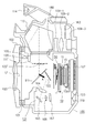
図1は、本実施形態に係るレンズ交換式デジタル一眼レフカメラ(以下、D-SLRと称する)の構成を示す概略構成図である。D-SLRは、CCDやCMOSセンサ等の撮像素子を用いた単板式のデジタルカラーカメラであり、撮像素子を連続的又は単発的に駆動して動画像又は静止画像を表わす画像信号を得る。撮像素子は、露光した光を画素毎に電気信号に変換して受光量に応じた電荷を蓄積し、蓄積された電荷を読み出すタイプのエリアセンサである。
Preferred embodiments of the present invention will be described below with reference to the accompanying drawings.
FIG. 1 is a schematic configuration diagram illustrating a configuration of a lens interchangeable digital single-lens reflex camera (hereinafter referred to as D-SLR) according to the present embodiment. The D-SLR is a single-plate digital color camera using an image sensor such as a CCD or a CMOS sensor, and obtains an image signal representing a moving image or a still image by driving the image sensor continuously or once. The imaging element is an area sensor of a type that converts exposed light into an electrical signal for each pixel, accumulates charges according to the amount of received light, and reads the accumulated charges.
具体的に説明すると、カメラ本体100のマウント機構101にはレンズユニット102が着脱可能に装着され、レンズユニット102がカメラ本体100に電気的、機械的に接続される。焦点距離の異なるレンズユニット102をカメラ本体100に装着することによって、様々な画角の撮影画面を得ることが可能である。
More specifically, the
レンズユニット102が備える撮影光学系103からフォーカルプレンシャッタ50を経て撮像部10に至る光路(光軸)L1が形成される。フォーカルプレンシャッタ50は、撮像部10に入射する光量を調節する。光軸L1上には、フォーカルプレンシャッタ50の後方に、赤外カットフィルタや、水晶等の位相板が積層された光学素子11が配置され、更にその後方に撮像部10が配置される。光学素子11は、撮像部10に含まれる固体撮像素子15b上に物体像(光学像)の必要以上に高い空間周波数成分が伝達されないように撮影光学系103のカットオフ周波数を制限する。
An optical path (optical axis) L1 from the photographing
固体撮像素子15bは、例えば増幅型固体撮像素子の1つであるCMOSプロセスコンパチブルのセンサ(以下、CMOSセンサと略す)である。固体撮像素子15bから読み出された信号は、所定の処理が施された後、画像データとしてディスプレイユニット107に表示される。ディスプレイユニット107はカメラ本体100の背面に配設されており、ユーザはディスプレイユニット107での表示を直接観察できるようになっている。ディスプレイユニット107を有機EL空間変調素子や液晶空間変調素子、微粒子の電気泳動を利用した空間変調素子等により構成すれば、消費電力を小さくでき、かつ、ディスプレイユニット107の薄型化を図ることができる。これにより、D-SLRの省電力化及び小型化を図ることができる。
The solid-
CMOSセンサの特長の一つとして、エリアセンサ部のMOSトランジスタと撮像装置駆動回路、AD変換回路、画像処理回路といった周辺回路を同一工程で形成できるので、マスク枚数、プロセス工程がCCDと比較して大幅に削減することができる。また、任意の画素へのランダムアクセスが可能であり、ディスプレイ用に間引いた読み出しが容易であって、ディスプレイユニット107において高い表示レートでリアルタイム表示を行うことができる。固体撮像素子15bは、上述した特長を利用し、ディスプレイ画像出力動作(固体撮像素子15bの受光領域のうち一部を間引いた領域での読み出し)及び高精彩画像出力動作(全受光領域での読み出し)を行う。
One of the features of the CMOS sensor is that the MOS transistors in the area sensor and the peripheral circuits such as the imaging device drive circuit, AD converter circuit, and image processing circuit can be formed in the same process. It can be greatly reduced. In addition, random access to any pixel is possible, reading that is thinned out for display is easy, and real-time display can be performed on the
カメラ本体100内のミラーボックスには可動型のハーフミラー111が設置され、ハーフミラー111の背後(像面側)には可動型のサブミラー122が設置される。
A
ハーフミラー111は、第1の光路分割状態(図1中の実線)と、第2の光路分割状態(図1中の点線)とを取り得る。第1の光路分割状態は、撮影光学系103からの光束をペンタプリズム112の方向へ導くために、ハーフミラー111が光軸L1に対して45°の角度に保持される状態である。また、第2の光路分割状態は、撮影光学系103からの光束を撮像部10の方向へ導くために、ハーフミラー111が光軸L1上から退避した位置に保持される状態である。サブミラー122は、ハーフミラー111の保持部材に設けられた回転軸を中心に回転し、ハーフミラー111の動きに連動する。なお、ハーフミラー111の屈折率はおよそ15であり、厚さが0.5mmである。
The
第1の光路分割状態で、ハーフミラー111は、撮影光学系103からの光束のうち一部を反射させるとともに、残りを透過させる。撮影光学系103によって形成される物体像の予定結像面にはフォーカシングスクリーン105が配置されている。フォーカシングスクリーン105上に結像された物体像は、ファインダレンズ109−1〜109−3を介して観察することができる。これらフォーカシングスクリーン105、ペンタプリズム112及びファインダレンズ109−1〜109−3はファインダ光学系を構成する。なお、フォーカシングスクリーン105上には、光学ファインダ内情報表示ユニット180により特定の情報を表示させることができる。また、セルフタイマー撮影時にファインダ光学系からの逆入光が固体撮像素子15bに入射してゴーストとなるのを防ぐためにアイピースシャッタ163が設けられている。
In the first optical path division state, the
また、ハーフミラー111を透過した光束のうち光軸L1に近い光束はサブミラー122で反射し、焦点検出ユニット121に導かれる。焦点検出ユニット121は、サブミラー122からの光束を受光して位相差検出方式による焦点検出を行う。焦点検出ユニット121は、光束の取り込み窓となるコンデンサーレンズ164、反射ミラー165、再結像レンズ166、焦点検出用センサ167により構成される。第1の光路分割状態においてサブミラー122で反射した光束は、ミラーボックス下部のコンデンサーレンズ164に入射した後、反射ミラー165で偏向し、再結像レンズ166の作用によって焦点検出用センサ167上に物体の2次像を形成する。焦点検出用センサ167には少なくとも2つの画素列が備えられており、2つの画素列の出力信号波形間には、焦点検出視野上に撮影光学系103によって形成された物体像の結像状態に応じて、相対的に横シフトした状態が観測される。前ピン、後ピンでは出力信号波形のシフト方向が逆になり、相関演算等の手法を用いてこの位相差(シフト量)を方向を含めて検出するのが焦点検出の原理である。
Further, of the light beams transmitted through the
カメラ本体100の上部には可動式の閃光発光ユニット114が設置されている。閃光発光ユニット114は、カメラ本体100に収納される収納位置と、カメラ本体100から突出した発光位置との間で移動可能である。
A movable flash
また、カメラ本体100には、メインスイッチ119、レリーズボタン120、異物除去スイッチ123が備えられている。メインスイッチ119は、D-SLRを起動させるためのスイッチである。レリーズボタン120は、2段階で押圧操作されるボタンであり、半押し操作(SW1のON)で撮影準備動作(測光動作や焦点調節動作等)が開始され、全押し操作(SW2のON)で撮影動作(固体撮像素子15bから読み出された画像データの記録媒体への記録)が開始される。異物除去スイッチ123は、任意のタイミングで後述する異物除去動作を行うためのスイッチである。
The
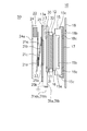
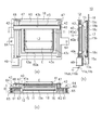
図2は、フォーカルプレンシャッタ50及び撮像部10の構成を説明するための断面図である。撮像部10は、光学素子11、保持部材12、圧電素子30、防塵ガラス31、除振部材32、マスク部材13、固体撮像装置15、シール部材16、基板17、保持板18を主な構成要素としてユニット化されている。
FIG. 2 is a cross-sectional view for explaining the configuration of the
光学素子11は、保持部材12により保持されている。防塵ガラス31は、光学素子11の前方に配置されている。圧電素子30は、防塵ガラス31に振動を加えることにより、防塵ガラス31の表面に付着した異物を除去する。すなわち、本実施形態では、圧電素子30が本発明でいう異物除去手段に相当し、防塵ガラス31が本発明でいう光学部材に相当する。
The
除振部材32は、防塵ガラス31と光学素子11との間を密閉すると共に、防塵ガラス31の振動が光学素子11に伝わるのを防止する。マスク部材13は、防塵ガラス31の光学有効範囲外に不要光が入射するのを防止するものであり、撮像のためにその略中央部に開口13aが形成されている。
The vibration isolation member 32 seals between the dust-
固体撮像装置15は、固体撮像素子15bと、固体撮像素子15bを保護するためのカバーガラス15aとを含んで構成される。シール部材16は、固体撮像装置15のカバーガラス15aと光学素子11との間を密封する。
The solid-
基板17には、固体撮像装置15の接続端子15cが接続するとともに、D-SLRの動作を制御する制御回路を構成する電気素子が搭載されている。
On the
保持板18は、その略中央部に開口18bを有すると共に、固体撮像装置15との接合部18cを有し、この接合部18cにて半田付け等により固体撮像装置15と一体化している。保持板18は、固体撮像装置15と一体化した状態で、不図示のシャーシにビス等によって固定される。
The holding
ここで、詳細は後述するが、防塵ガラス31の表面には、GND線31a及び31bが配設されている。これらGND線31a及び31bは、切換手段たるスイッチ31ab及び31bbを介して基板17の不図示のGND部もしくはD-SLRのGND電位部に接続する。すなわち、防塵ガラス31の表面は接地されている構造となっている。
Here, although details will be described later,
一方、撮像部10の前方に配置されるフォーカルプレンシャッタ50は、先幕21、後幕22、先幕21及び後幕22の駆動スペースを分割する中間板23、後幕22の押え板24、先幕21の押え板であるカバー板25を主な構成要素としてユニット化されている。
On the other hand, the
先幕21は、複数のシャッタ羽根21a〜21dにより構成される。後幕22も、同じく複数のシャッタ羽根により構成される。先幕21及び後幕22を構成するシャッタ羽根は、それぞれ単一もしくは複数の不図示の駆動レバーによって一体的に開閉動作を行うようになっている。また、先幕21及び後幕22を構成するシャッタ羽根は、開閉動作時の摩擦負荷や摩擦帯電を防止するために、導電性の材料で形成されていたり、その表面に摺動性を向上させたり帯電を防止したりする表面処理が施されていたりする。
The front curtain 21 includes a plurality of
押え板24には、撮像のためにその略中央部に開口24aが形成されている。カバー板25には、撮像のためにその略中央部に開口25aが形成されている。カバー板25は、導電性の部材であると共に接続部25bを有し、該接続部25bはGND線31a及び31bと同じく基板17の不図示のGND部もしくはD-SLRのGND電位部に不図示のビス等によって接続する。すなわち、カバー板25は接地されている構造となっている。カバー板25は、先幕21を構成するシャッタ羽根21aの表面と当接した状態でフォーカルプレンシャッタ50を構成する。これにより、シャッタ羽根21aが接地されているので、先幕21全体が接地状態になる。
The
以上の構成により、対面する先幕21及び防塵ガラス31の表面は共に接地状態になるので、両者の間には電位差が生じない(同電位となっている)。これにより、先幕21と防塵ガラス31との間の空間に塵埃等の異物が存在しても、異物はどちらにも吸引されることがないので、防塵ガラス31の表面に異物が付着するのを抑制することができる。
With the above configuration, since the front curtain 21 and the surface of the dust-
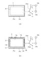
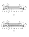
図3は、防塵ガラス31の正面図である。より詳細には、図3(a)は防塵ガラス31の正面図、図3(b)は防塵ガラス31にマスク部材13を配設した状態の正面図である。図3(a)に示すように、防塵ガラス31の表面のうち、光学有効範囲Eの外側には、GND線31a及び31bが配設される。GND線31a及び31bは、防塵ガラス31の略全周にわたって所定のギャップを持って略平行に配置されている。また、図3(b)に示すように、GND線31a及び31bは、マスク部材13に形成された開口部13bを介して露出する。
FIG. 3 is a front view of the dust-
通常、GND線31a及び31bはスイッチ31ab及び31bbにより接地状態にあるが、後述するようにD-SLR内の湿度検出時には、GND線31a及び31bがスイッチ31ab及び31bbにより電源34aに接続される。スイッチ31bb側には電流計34bが接続されており、電流計34bにより検出された電流値と電源34aの電圧値から抵抗値を算出し、その抵抗値を後述のカメラシステム制御回路135に出力する。
Normally, the GND lines 31a and 31b are grounded by the switches 31ab and 31bb. However, as described later, when detecting the humidity in the D-SLR, the GND lines 31a and 31b are connected to the
図4は、D-SLRのカメラシステムの電気的構成を示すブロック図である。なお、図1で説明した構成要素と同じものには同一の符号を付す。 FIG. 4 is a block diagram showing an electrical configuration of the D-SLR camera system. In addition, the same code | symbol is attached | subjected to the same thing as the component demonstrated in FIG.
まず、物体像の撮像、記録に関する部分から説明する。カメラシステムは、撮像系、画像処理系、記録再生系及び制御系を有する。撮像系は、撮影光学系103及び固体撮像装置15を有する。画像処理系は、A/D変換器130、RGB画像処理回路131及びYC処理回路132を有する。記録再生系は、記録処理回路133及び再生処理回路134を有する。制御系は、カメラシステム制御回路(制御手段)135、操作検出回路136、撮像素子駆動回路137を有する。
First, an explanation will be given from the part related to the imaging and recording of object images. The camera system has an imaging system, an image processing system, a recording / reproducing system, and a control system. The imaging system includes a photographing
撮像系は、物体からの光を、撮影光学系103を介して固体撮像装置15の撮像面に結像させる光学処理系である。撮影光学系103内に設けられた絞り104の駆動を制御するとともに、必要に応じてシャッタ制御回路145によりフォーカルプレンシャッタ50の駆動を行うことによって、適切な光量の物体光を固体撮像装置15で受光させることができる。
The imaging system is an optical processing system that forms an image of light from an object on the imaging surface of the solid-
固体撮像装置15の固体撮像素子15bとして、正方画素が長辺方向に3700個、短辺方向に2800個並べられ、合計約1000万個の画素数を有する撮像素子が用いられている。各画素にはR(赤色)G(緑色)B(青色)のカラーフィルタが交互に配置され、4画素が一組となるいわゆるベイヤー配列を構成している。ベイヤー配列では、観察者が画像を見たときに強く感じやすいGの画素をRやBの画素よりも多く配置することで、総合的な画像性能を上げている。一般に、この方式の撮像素子を用いる画像処理では、輝度信号は主にGから生成し、色信号はR、G、Bから生成する。
As the solid-state
固体撮像素子15bから読み出された信号は、A/D変換器130を介して画像処理系に供給され、この画像処理系での画像処理によって画像データが生成される。A/D変換器130は、固体撮像素子15bの各画素から読み出された信号の振幅に応じて、例えば固体撮像素子15bの出力信号を10ビットのデジタル信号に変換して出力する信号変換回路であり、以降の画像処理はデジタル処理にて実行される。
The signal read from the solid-
画像処理系は、R、G、Bのデジタル信号から所望の形式の画像信号を得る信号処理回路であり、R、G、Bの色信号を輝度信号Y及び色差信号(R−Y)、(B−Y)にて表わされるYC信号等に変換する。RGB画像処理回路131は、A/D変換器130の出力信号を処理する信号処理回路であり、ホワイトバランス回路、ガンマ補正回路、補間演算による高解像度化を行う補間演算回路を有する。YC処理回路132は、輝度信号Y及び色差信号R−Y、B−Yを生成する信号処理回路である。このYC処理回路132は、高域輝度信号YHを生成する高域輝度信号発生回路、低域輝度信号YLを生成する低域輝度信号発生回路及び色差信号R−Y、B−Yを生成する色差信号発生回路を有する。輝度信号Yは、高域輝度信号YHと低域輝度信号YLを合成することによって形成される。
The image processing system is a signal processing circuit that obtains an image signal in a desired format from R, G, and B digital signals. The R, G, and B color signals are converted into a luminance signal Y and a color difference signal (R−Y), ( (B-Y) and the like. The RGB
記録再生系は、不図示のメモリへの画像信号の出力と、ディスプレイユニット107への画像信号の出力とを行う処理系である。記録処理回路133はメモリへの画像信号の書き込み処理及び読み出し処理を行い、再生処理回路134はメモリから読み出した画像信号を再生して、ディスプレイユニット107に出力する。
The recording / reproducing system is a processing system that outputs an image signal to a memory (not shown) and outputs an image signal to the
記録処理回路133は、静止画データ及び動画データを表わすYC信号を所定の圧縮形式にて圧縮するとともに、圧縮されたデータを伸張させる圧縮伸張回路を内部に有する。圧縮伸張回路は、信号処理のためのフレームメモリ等を有し、このフレームメモリに画像処理系からのYC信号をフレーム毎に蓄積し、複数のブロックのうち各ブロックから蓄積された信号を読み出して圧縮符号化する。圧縮符号化は、例えばブロック毎の画像信号を2次元直交変換、正規化及びハフマン符号化することにより行われる。
The
再生処理回路134は、輝度信号Y及び色差信号R−Y、B−Yをマトリクス変換して、例えばRGB信号に変換する回路である。再生処理回路134により変換された信号はディスプレイユニット107に出力され、可視画像として表示(再生)される。再生処理回路134及びディスプレイユニット107は、Bluetooth(登録商標)等の無線通信を介して接続されていてもよく、このように構成すれば、このカメラで撮像された画像を離れたところからモニタすることができる。
The
一方、制御系における操作検出回路136は、メインスイッチ119、レリーズボタン120、異物除去スイッチ123等(他のスイッチは不図示)の操作を検出して、この検出結果をカメラシステム制御回路135に出力する。カメラシステム制御回路135は、操作検出回路136からの検出信号を受けることで、検出結果に応じた動作を行う。また、カメラシステム制御回路135は、撮像動作を行う際のタイミング信号を生成して、撮像素子駆動回路137に出力する。撮像素子駆動回路137は、カメラシステム制御回路135からの制御信号を受けることで固体撮像装置15を駆動させるための駆動信号を生成する。情報表示回路142は、カメラシステム制御回路135からの制御信号を受けて光学ファインダ内情報表示ユニット180の駆動を制御する。
On the other hand, the
制御系は、D-SLRに設けられた各種スイッチの操作に応じて撮像系、画像処理系及び記録再生系での駆動を制御する。例えば、レリーズボタン120の操作によってSW2がONとなった場合、制御系(カメラシステム制御回路135)は、固体撮像装置15の駆動、RGB画像処理回路131の動作、記録処理回路133の圧縮処理等を制御する。さらに、制御系は、情報表示回路142を介して光学ファインダ内情報表示ユニット180の駆動を制御することによって、光学ファインダ内での表示(表示セグメントの状態)を変更する。
The control system controls driving in the imaging system, the image processing system, and the recording / reproducing system in accordance with operations of various switches provided in the D-SLR. For example, when SW2 is turned ON by operating the
次に、撮影光学系103の焦点調節動作に関して説明する。カメラシステム制御回路135は、AF制御回路140と接続する。また、レンズユニット102をカメラ本体100に装着することで、カメラシステム制御回路135は、マウント接点100a、102aを介してレンズユニット102内のレンズシステム制御回路141と接続される。AF制御回路140及びレンズシステム制御回路141と、カメラシステム制御回路135とは、特定の処理の際に必要となるデータを相互に通信する。
Next, the focus adjustment operation of the photographic
焦点検出ユニット121(焦点検出用センサ167)は、撮影画面内の所定位置に設けられた焦点検出領域での検出信号をAF制御回路140に出力する。AF制御回路140は、焦点検出ユニット121からの出力信号に基づいて焦点検出信号を生成し、撮影光学系103の焦点調節状態(デフォーカス量)を検出する。そして、AF制御回路140は、検出したデフォーカス量を撮影光学系103の一部の要素であるフォーカスレンズの駆動量に変換し、フォーカスレンズの駆動量に関する情報を、カメラシステム制御回路135を介してレンズシステム制御回路141に送信する。
The focus detection unit 121 (focus detection sensor 167) outputs a detection signal in a focus detection area provided at a predetermined position in the shooting screen to the
ここで、移動する物体に対して焦点調節を行う場合、AF制御回路140は、レリーズボタン120が全押し操作されてから実際の撮像制御が開始されるまでのタイムラグを勘案して、フォーカスレンズの適切な停止位置を予測する。そして、予測した停止位置へのフォーカスレンズの駆動量に関する情報をレンズシステム制御回路141に送信する。
Here, when the focus adjustment is performed on the moving object, the
一方、カメラシステム制御回路135は、固体撮像装置15の出力信号に基づいて物体の輝度が低く、十分な焦点検出精度が得られないと判定したときには、閃光発光ユニット114又はD-SLRに設けられた不図示の白色LEDや蛍光管を駆動することによって物体を照明する。
On the other hand, the camera
レンズシステム制御回路141は、カメラシステム制御回路135からフォーカスレンズの駆動量に関する情報を受信すると、レンズユニット102内に配置されたAFモータ147の駆動を制御する。これにより、不図示の駆動機構を介してフォーカスレンズを上記駆動量の分だけ光軸L1方向に移動させる。その結果、撮影光学系103が合焦状態となる。なお、フォーカスレンズが液体レンズ等で構成されている場合には、界面形状を変化させることになる。
When the lens
また、レンズシステム制御回路141は、カメラシステム制御回路135から露出値(絞り値)に関する情報を受信すると、レンズユニット102内の絞り駆動アクチュエータ143の駆動を制御する。これにより、上記絞り値に応じた絞り開口径となるように絞り104を動作させる。また、シャッタ制御回路145は、カメラシステム制御回路135からのシャッタ速度に関する情報を受信すると、フォーカルプレンシャッタ50の駆動源51の駆動を制御する。これにより、上記シャッタ速度になるようにフォーカルプレンシャッタ50を動作させる。このフォーカルプレンシャッタ50と絞り104の動作により、適切な光量の物体光を像面側に向かわせることができる。
When the lens
AF制御回路140において物体にピントが合ったことが検出されると、この情報はカメラシステム制御回路135に送信される。このとき、レリーズボタン120の全押し操作によってSW2がON状態になれば、上述したように撮像系、画像処理系及び記録再生系によって撮影動作が行われる。
When the
接続端子138は、外部のコンピュータ等に接続され、データの送受信を行うために規格化された接続端子である。このようにしたカメラシステムは、不図示の小型燃料電池からの電力供給を受けて駆動する。
The
また、PZT制御部33は、防塵ガラス31を振動させる圧電素子30の駆動を制御する。
The
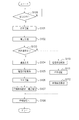
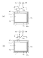
図5は、結露検出時の動作を示すフローチャートである。また、図6(a)〜(c)は、結露検出時の防塵ガラス31の表面に設けられたGND線の接続状態を説明するための図である。図5のフローチャート及び図6(a)〜(c)の動作説明図を用いて、例えばD-SLRの電源ON時に結露検出を実行する場合の動作について説明する。
FIG. 5 is a flowchart showing the operation when dew condensation is detected. FIGS. 6A to 6C are diagrams for explaining the connection state of the GND lines provided on the surface of the dust-
ステップS100で、カメラシステム制御回路135は、メインスイッチ119が操作されてD-SLRの電源がONになったか否かの検出を行う。メインスイッチ119の操作により電源がONになったことを検出したら、D-SLRはスリープモードを脱してステップS101へと進む。このとき、図6(a)に示すように、スイッチ31ab及び31bbは接地位置にあり、防塵ガラス31の表面はGND電位になっている。この状態では、上述したように、先幕21と防塵ガラス31の表面との間に電位差が生じないので、防塵ガラス31の表面への異物付着が抑制される。
In step S100, the camera
次にステップS101で、スイッチ31ab及び31bbを接地位置から切り換えて、図6(b)に示すように、GND線31a及び31bを電源34aに接続する。
Next, in step S101, the switches 31ab and 31bb are switched from the ground position, and the GND lines 31a and 31b are connected to the
次にステップS102で、電源34aから所定の電圧を印加して、電流計34bにより検出された電流値と電源34aの電圧値とからGND線31a及び31b間の抵抗値を算出(検知)する。
Next, in step S102, a predetermined voltage is applied from the
次にステップS103で、カメラシステム制御回路135は、ステップS102において検知した抵抗値が、不図示のメモリ部に記憶された初期抵抗値に比べて所定量だけ変化しているか否かの検出を行う。
In step S103, the camera
ここで、図6(b)に示した状態であれば、GND線31a及び31b間の抵抗値は変化しない。ところが、図6(c)に示すように、防塵ガラス31の表面に結露が発生すると、GND線31a及び31b間のギャップに結露した液滴Dが付着するため(範囲Wを参照)、GND線31a及び31b間の抵抗値が小さくなる。すなわち、ステップS103において抵抗値が所定量だけ変化している場合は、防塵ガラス31の表面に結露が発生したと判定し、ステップS104へと進む。一方、ステップS103において抵抗値の変化がない場合は、防塵ガラス31の表面に結露が発生していないと判定し、ステップS110へと進む。
Here, in the state shown in FIG. 6B, the resistance value between the GND lines 31a and 31b does not change. However, as shown in FIG. 6C, when condensation occurs on the surface of the dust-
ステップS104では、ステップS103において防塵ガラス31の表面に結露が発生したと判定されたので、防塵ガラス31の表面に付着した異物の除去動作を通常時の異物除去動作とは異ならせる旨の通告表示をディスプレイユニット107に表示する。
In step S104, since it is determined in step S103 that condensation has occurred on the surface of the dust-
続くステップS105では、電源34aを制御し、GND線31a及び31bに電圧を印加する状態を解除して、ステップS106へと進む。
In subsequent step S105, the
続くステップS106では、スイッチ31ab及び31bbを接地位置に切り換えて(図6(a)の状態)、ステップS107へと進む。 In the subsequent step S106, the switches 31ab and 31bb are switched to the ground position (state shown in FIG. 6A), and the process proceeds to step S107.
続くステップS107では、結露発生時の異物除去動作を実行する。防塵ガラス31の表面に結露が発生していると、付着力の増加により、通常時の異物除去動作を行っても全ての異物が除去されないおそれがある。そこで、カメラシステム制御回路135は、PZT制御部33を介して、例えば通常の倍の電圧を圧電素子30に印加したり、通常よりも長い時間圧電素子30により加振させたりする制御を行うことにより、結露により除去しにくくなった異物を確実に除去するようにする。その後、ステップS108へと進む。
In a succeeding step S107, a foreign matter removing operation is performed when condensation occurs. If dew condensation occurs on the surface of the dust-
一方、ステップS110では、電源34aを制御し、GND線31a及び31bに電圧を印加する状態を解除して、ステップS111へと進む。
On the other hand, in step S110, the
続くステップS111では、スイッチ31ab及び31bbの接地位置に切り換えて(図6(a)の状態)、ステップS112へと進む。 In the subsequent step S111, the switches 31ab and 31bb are switched to the ground positions (the state shown in FIG. 6A), and the process proceeds to step S112.
続くステップS112では、通常時の異物除去動作を実行する。その後、ステップS108へと進む。 In the subsequent step S112, a normal foreign matter removing operation is executed. Thereafter, the process proceeds to step S108.
ステップS108では、ステップS107又はステップS112での異物除去動作が完了しているので待機状態となり、ユーザによるメインスイッチ119やレリーズボタン120等の各種スイッチ類の操作を検出する。
In step S108, since the foreign substance removal operation in step S107 or step S112 has been completed, the standby state is entered, and the operation of various switches such as the
以上述べた構成により、次のような効果が得られる。防塵ガラス31の表面に結露が発生した状態では、通常の倍の電圧を圧電素子30に印加したり、異物除去動作の時間を長くしたりすることにより、防塵ガラス31の表面に付着した異物を確実に除去することができる。したがって、光学機器の環境に依らずに焦点面近傍の光学部材の表面に付着した異物を効果的に除去することが可能となる。
With the configuration described above, the following effects can be obtained. In a state where condensation occurs on the surface of the dust-
しかも、防塵ガラス31の表面に結露が発生したかどうかは、防塵ガラス31の表面を接地状態にする導電部(GND線31a及び31b)を利用して検出するので、コスト及びスペースの面で不利にならず、かつ、光学的な不具合が発生することもない。
In addition, whether or not condensation has occurred on the surface of the dust-
(第2の実施形態)
第2の実施形態では、異物除去手段として、光学素子11の表面に接触しながら移動することにより、光学素子11の表面を直接払拭し、表面に付着した異物を除去する異物除去部材を有する光学機器を説明する。なお、以下では、第1の実施形態で説明したものと同様の構成要素には同一の符号を付し、その説明を省略する。
(Second Embodiment)
In the second embodiment, as a foreign matter removing means, an optical device having a foreign matter removing member that wipes the surface of the
図7は、本実施形態に係るレンズ交換式デジタル一眼レフカメラ(D-SLR)の構成を示す概略構成図である。図7において、40は異物除去部材であり、光学素子11の表面に接触しながら移動することにより、その表面に付着した異物を除去する。
FIG. 7 is a schematic configuration diagram showing the configuration of the interchangeable lens digital single-lens reflex camera (D-SLR) according to the present embodiment. In FIG. 7,
図8は、撮像部10の構成を説明するための断面図である。また、図9は、異物除去部材40の断面図である。上記第1の実施形態では、防塵ガラス31が本発明でいう光学部材に相当するが、本実施形態では、防塵ガラス31を設置しておらず、光学素子11が本発明でいう光学部材に相当する。
FIG. 8 is a cross-sectional view for explaining the configuration of the
支持板43は、光学素子11の表面と当接した状態で光学素子11と保持部材12とを一体化させる。支持板43には開口幅L2の開口部が形成されており、短辺(左右辺)側の開口縁43aは光学素子11の光学有効範囲Eの外側に位置する。また、長辺(上辺)側の開口縁43bは、開口縁43aと同一平面には設けられておらず、光学素子11の端面側に設けられている。これにより、後述する異物除去部材40の移動に干渉するのを避けるとともに、光学素子11の入光面の略全域を払拭することができる。
The
異物除去部材40は、図9に示すように、板状の基材40dと、基材40dのうち光学素子11の対向面側に接着層を介して設けられた繊維40eとにより構成される。このようにした異物除去部材40は、後述するリードスクリュ48及びモータ49により、図8(b)に示す位置40aから、光学素子11の表面に対向する位置40bを通過して、位置40cまで移動可能となっている。すなわち、異物除去部材40は光学素子11の入光面の略全域に対して移動可能であり、その移動過程において、繊維40eにより光学素子11の入光面の略全域に付着した異物を払拭して除去する。
As shown in FIG. 9, the foreign
異物除去部材40の基材40dは金属製であり、繊維40eも少なくともその一部が導電性を有するとともに、接着層にも導電性の接着剤が用いられる。これにより、異物除去部材40は、図8(a)に示すように、D-SLRの筐体もしくは基板17上に設けられたGND端子に接続されることによって接地され、異物を除去するための払拭動作により光学素子11が帯電するのを防ぐことができる。したがって、帯電により光学素子11の表面に異物を引き寄せることもなくなるので、異物の付着を抑制することもできる。
The
異物除去部材40まわりについて詳細に説明する。保持板18と対向するようにベース板60が配置される。ベース板60には、光学素子11に対応する開口60aが形成されている。
The area around the foreign
ベース板60のうち保持板18との対向面と逆側の面には、開口60aを挟んで両サイドにガイド軸47が設置され、一方のサイドにはガイド軸47と平行にリードスクリュ48がさらに設置される。異物除去部材40の両端にはガイド部42が設けられており、一端のガイド部42はガイド軸47を挿通するとともにリードスクリュ48に係合し、他端のガイド部42はガイド軸47に挿通する。モータ49によりリードスクリュ48が回転すると、異物除去部材40はガイド軸47にガイドされながら位置40a〜40cを移動する。
A
また、図8(c)に示すように、保持板18の両サイドには永久磁石62が設置されるとともに、ベース板60のうち保持板18との対向面には、各永久磁石62に対向する形でコイル61が設けられる。
Further, as shown in FIG. 8C,
さらに、保持板18には永久磁石62よりも外側位置に軸64が立設されており、これら軸64がベース板60を貫通する。軸64には付勢手段としてコイルスプリング65が組み付けられており、ベース板60は軸64にガイドされながら光軸方向(図8(c)の矢印B方向)に付勢されている。
Furthermore,
コイル61に通電していないとき、図8(c)に示すように、コイルスプリング65の付勢力により、ベース板60は保持板18から離れた状態にある。すなわち、ベース板60に取り付けられている異物除去部材40が光学素子11の表面から離れた状態にあり、繊維40eが光学素子11の表面に接触していない。このようにD-SLRの通常の撮影時や保管時には、異物除去部材40が光学素子11から離れた状態に保たれるので、繊維40eに曲げクセが付くような不具合が発生しない。
When the
図8(c)の状態からコイル61に通電すると、その磁気作用によりコイル61が永久磁石62に吸引され、ベース板60はコイルスプリング65の付勢力に抗して矢印Bとは逆方向に移動する。すなわち、ベース板60に取り付けられている異物除去部材40が光学素子11の表面に近づいた状態となり、繊維40eを光学素子11の表面に接触させることができる。このようにD-SLRの異物除去動作時等には、異物除去部材40を光学素子11の表面に接触させた状態とすることができる。
When the
また、D-SLRの筐体には、異物除去部材40により光学素子11の表面から除去した異物を捕獲するための不図示の吸着部(具体的には粘着テープ等)が設けられる。
Further, the D-SLR housing is provided with an unillustrated suction portion (specifically, an adhesive tape or the like) for capturing the foreign matter removed from the surface of the
図10は、光学素子11の正面図である。より詳細には、図10(a)は光学素子11の正面図、図10(b)は光学素子11に支持板43を配設した状態の正面図である。図10(b)に示すように、光学素子11の表面のうち、光学有効範囲Eの外側には、GND線11a及び11bが配設される。GND線11aは反時計周り方向に延伸し、GND線11bは時計回り方向に延伸することにより、光学素子11の略全周にわたって配置されるが、GND線11a及び11bの先端において互いに離間した状態となっている(検出部11c)。また、図10(b)に示すように、GND線11a及び11b、並びに検出部11cは、支持板43に形成された開口部43cを介して露出する。
FIG. 10 is a front view of the
上記第1の実施形態と同様、通常、GND線11a及び11bはスイッチ11ab及び11bbにより接地状態にあるが、後述するようにD-SLR内の湿度検出時には、GND線11a及び11bがスイッチ11ab及び11bbにより電源34aに接続される。スイッチ11bb側には電流計34bが接続されており、電流計34bにより検出された電流値と電源34aの電圧値から抵抗値を算出し、その抵抗値を後述のカメラシステム制御回路135に出力する。
As in the first embodiment, the GND lines 11a and 11b are normally grounded by the switches 11ab and 11bb. However, as described later, when detecting humidity in the D-SLR, the GND lines 11a and 11b are connected to the switches 11ab and 11bb. 11bb is connected to the
図11は、D-SLRのカメラシステムの電気的構成を示すブロック図である。ここで、上記第1の実施形態や図7で説明した構成要素と同様のものには同一符号を付す。本実施形態では、モータ49の駆動を制御するモータ制御部46を備える。
FIG. 11 is a block diagram showing an electrical configuration of a D-SLR camera system. Here, the same components as those described in the first embodiment and FIG. In the present embodiment, a
図12は、結露検出時の動作を示すフローチャートである。また、図13(a)、(b)は、異物除去部材40の動作を説明するための図である。また、図14(a)〜(c)は、結露検出時の光学素子11の表面に設けられたGND線の接続状態を説明するための図である。また、図15は、GND線11a及び11bの導通状態を説明するための部分拡大図である。図12のフローチャート及び図13〜15の動作説明図を用いて、例えばD-SLRの電源ON時に結露検出を実行する場合の動作について説明する。
FIG. 12 is a flowchart showing an operation when dew condensation is detected. 13A and 13B are diagrams for explaining the operation of the foreign
ステップS200で、カメラシステム制御回路135は、メインスイッチ119が操作されてD-SLRの電源がONになったか否かの検出を行う。メインスイッチ119の操作により電源がONになったことを検出したら、D-SLRはスリープモードを脱してステップS201へと進む。このとき、図14(a)に示すように、スイッチ11ab及び11bbは接地位置にあり、光学素子11の表面はGND電位になっている。この状態では、第1の実施形態で述べたのと同様に、先幕21と光学素子11の表面との間に電位差が生じないので、光学素子11の表面への異物付着が抑制される。また、このとき、異物除去部材40は位置40aに位置している(図8(a)を参照)。
In step S200, the camera
次にステップS201で、スイッチ21ab及び21bbを接地位置から切り換えて、図14(b)に示すように、GND線11a及び11bを電源34aに接続する。
In step S201, the switches 21ab and 21bb are switched from the ground position, and the GND lines 11a and 11b are connected to the
次にステップS202で、電源34aから所定の電圧を印加して、電流計34bにより検出された電流値と電源34aの電圧値とからGND線11a及び11b間の抵抗値を算出(検知)する。
Next, in step S202, a predetermined voltage is applied from the
次にステップS203で、カメラシステム制御回路135は、ステップS202において検知した抵抗値が、不図示のメモリ部に記憶された初期抵抗値に比べて所定量だけ変化しているか否かの検出を行う。
In step S203, the camera
ここで、図14(b)に示した状態であれば、GND線11a及び11b間の抵抗値は変化しない。ところが、図15に示すように、光学素子11の表面に結露が発生すると、GND線11a及び11b間のギャップに結露した液滴41aが付着するため、GND線11a及び11b間の抵抗値が小さくなる。すなわち、ステップS203において抵抗値が所定量だけ変化している場合は、光学素子11の表面に結露が発生したと判定し、ステップS204へと進む。一方、ステップS203において抵抗値の変化がない場合は、光学素子11の表面に結露が発生していないと判定し、ステップS220へと進む。
Here, in the state shown in FIG. 14B, the resistance value between the GND lines 11a and 11b does not change. However, as shown in FIG. 15, when condensation occurs on the surface of the
ステップS204では、ステップS203において光学素子11の表面に結露が発生したと判定されたので、光学素子11の表面の結露を除去する旨の通告表示をディスプレイユニット107に表示する。
In step S204, since it is determined in step S203 that condensation has occurred on the surface of the
続くステップS205では、コイル61に通電する。これにより、図13(b)に示すように、磁気作用によりコイル61が永久磁石62に吸引され、ベース板60がコイルスプリング65の付勢力に抗して矢印C方向に移動して、異物除去部材40の繊維40eが光学素子11の表面に接触することになる。その結果、上述したように繊維40eの一部が導電性であるので、GND線11a及び11b間が繊維40eにより導通する。これにより、電源34aから所定の電圧をGND線11a及び11bに印加することで、光学素子11の表面を加熱することができ、光学素子11の表面の結露を除去することができる。
In subsequent step S205, the
続くステップS206では、カメラシステム制御回路135が有する不図示のタイマ部にて、所定秒時のカウントを行い、電源34aからの電圧印加を所定時間だけ続ける。
In the subsequent step S206, a timer unit (not shown) included in the camera
続くステップS207では、コイル61への通電を停止する。これにより、図13(a)に示すように、ベース板60がコイルスプリング65の付勢力により保持板18から離れ、異物除去部材40の繊維40eが光学素子11の表面から離れることになる。
In continuing step S207, the electricity supply to the
続くステップS208では、上記ステップS203と同様、電流計34bにより検出された電流値と電源34aの電圧値とから算出されるGND線11a及び11b間の抵抗値が、不図示のメモリ部に記憶された初期抵抗値に比べて所定量だけ変化しているか否かの検出を行う。これは、ステップS206における結露除去動作により、光学素子11の結露が除去されて、抵抗値が初期抵抗値になっていないかどうかを確認するためである。
In the subsequent step S208, as in step S203, the resistance value between the GND lines 11a and 11b calculated from the current value detected by the
ステップS208において検知された抵抗値が初期抵抗値と異なる場合、つまりステップS206における結露除去が不十分だった場合は、ステップS205に戻って、再度結露除去動作を行う。一方、ステップS208において検知された抵抗値が初期抵抗値と略同等の場合、ステップS206における結露除去が十分であったとして、ステップS204において表示した通告表示を解除した上で(ステップS210)、ステップS220へと進む。 If the resistance value detected in step S208 is different from the initial resistance value, that is, if the condensation removal in step S206 is insufficient, the process returns to step S205 and the condensation removal operation is performed again. On the other hand, if the resistance value detected in step S208 is substantially equal to the initial resistance value, the notification display displayed in step S204 is canceled (step S210), assuming that condensation removal in step S206 is sufficient (step S210). Proceed to S220.
ステップS220では、電源34aを制御し、GND線11a及び11bに電圧を印加する状態を解除して、ステップS221へと進む。
In step S220, the
続くステップS221では、スイッチ11ab及び11bbの接地位置に切り換えて(図14(a)の状態)、ステップS222へと進む。 In the following step S221, the switches 11ab and 11bb are switched to the ground positions (the state shown in FIG. 14A), and the process proceeds to step S222.
続くステップS222では、光学素子11の表面が結露していないので、モータ制御部46によりモータ49を駆動する。これにより、上述したように異物除去部材40が光学素子11の表面に接触しながら位置40aから位置40cまで往復動作するので、光学素子11の表面に付着した異物を除去することができる。その後、ステップS223へと進む。なお、異物除去動作時には、コイル61に通電し、異物除去部材40を光学素子11の表面に接触させることは既述したとおりである。
In the subsequent step S222, since the surface of the
ステップS223では、ステップS222での異物除去動作が完了しているので待機状態となり、ユーザによるメインスイッチ119やレリーズボタン120等の各種スイッチ類の操作を検出する。
In step S223, since the foreign substance removal operation in step S222 is completed, a standby state is entered, and the operation of various switches such as the
以上述べた構成により、次のような効果が得られる。光学素子11の表面に結露が発生した状態では、GND線11a及び11bに通電することにより、光学素子11の表面を加熱して結露を除去してから異物除去動作を行うことができる。したがって、光学機器の環境に依らずに焦点面近傍の光学部材の表面に付着した異物を効果的に除去することが可能となる。
With the configuration described above, the following effects can be obtained. In the state where condensation occurs on the surface of the
しかも、光学素子11の表面に結露が発生したかどうかは、光学素子11の表面を接地状態にする導電部(GND線11a及び11b)を利用して検出するので、コスト及びスペースの面で不利にならず、かつ、光学的な不具合が発生することもない。
In addition, whether or not condensation has occurred on the surface of the
以上述べた第1、2の実施形態では、防塵ガラス31もしくは光学素子11の表面の結露状態を検出したが、これに限定されるものではない。例えば、図16に示すように、フォーカルプレンシャッタ50と固体撮像装置15のカバーガラス15aとが近接しているようなデジタルカラーカメラの場合、フォーカルプレンシャッタ50と固定撮像装置15との間に異物除去部材40が配設される。この場合は、固体撮像装置15のカバーガラス15aの表面にGND線11a及び11bを設けることにより、カバーガラス15aの表面の結露状態が検出可能になる。
In the first and second embodiments described above, the dew condensation state on the surface of the dust-
また、第1、2の実施形態では、GND線31a(11a)及び31b(11b)間の抵抗値を検知するようにしたが、例えばGND線31a(11a)及び31b(11b)間の容量(静電容量(電気容量))の容量を検知することでも同様の効果が得られる。GND線31a(11a)及び31b(11b)間に結露により液滴が付着した場合には、GND線31a(11a)及び31b(11b)間の静電容量が変化するからである。
In the first and second embodiments, the resistance value between the
10:撮像部
11:光学素子
11a、11b:GND線
11ab、11bb:スイッチ
15:固体撮像装置
15b:固体撮像素子
30:圧電素子
31:防塵ガラス
31a、31b:GND線
31ab、31bb:スイッチ
34a:電源
34b:電流計
40:異物除去部材
135:カメラシステム制御回路
DESCRIPTION OF SYMBOLS 10: Imaging part 11:
Claims (4)
前記光学部材の表面のうち、光学有効範囲の外側の略全周にわたって配置される第1の導電部と、
前記第1の導電部と所定のギャップを保って、前記光学部材の表面のうち、前記光学有効範囲の外側の略全周にわたって配置される第2の導電部と、
前記光学部材の表面に配置され、前記光学部材の前記光学有効範囲を露出させる第1の開口部と前記第1の導電部および前記第2の導電部を露出させる第2の開口部が形成されるマスク部材と、
前記第1の導電部と前記第2の導電部との間に電圧を印加する電源と、
前記第1の導電部と前記第2の導電部とをともに接地電位に接続する状態と前記第1の導電部と前記第2の導電部との間に前記電源の電圧を印加する状態とに切り換える切換手段と、
前記切換手段により前記第1の導電部と前記第2の導電部との間に前記電源の電圧を印加する状態で、前記第1の導電部と前記第2の導電部との間の抵抗値又は容量を検知する検知手段とを備えたことを特徴とする光学機器。 An optical member;
Of the surface of the optical member, a first conductive portion disposed over substantially the entire circumference outside the optical effective range ;
A second conductive portion disposed over substantially the entire circumference outside the optical effective range of the surface of the optical member while maintaining a predetermined gap with the first conductive portion;
A first opening that is disposed on the surface of the optical member and exposes the optical effective range of the optical member, and a second opening that exposes the first conductive portion and the second conductive portion are formed. A mask member,
A power supply for applying a voltage between the first conductive portion and the second conductive portion ;
A state in which the first conductive portion and the second conductive portion are both connected to a ground potential, and a state in which the voltage of the power source is applied between the first conductive portion and the second conductive portion. Switching means for switching;
A resistance value between the first conductive portion and the second conductive portion in a state where the voltage of the power source is applied between the first conductive portion and the second conductive portion by the switching means. Or an optical device comprising a detecting means for detecting a capacity.
前記検知手段により検知される抵抗値又は容量に基づいて結露の発生を判定し、結露が発生したと判定した場合には、前記異物除去手段による異物除去動作を結露が発生していないと判定した場合の異物除去動作よりも異物除去能力の高い異物除去動作を実行する制御手段とを備えたことを特徴とする請求項1又は2に記載の光学機器。 Foreign matter removing means for removing foreign matter attached to the surface of the optical member;
The occurrence of condensation is determined based on the resistance value or the capacitance detected by the detection means, and when it is determined that condensation has occurred, the foreign substance removal operation by the foreign substance removal means is determined as no condensation has occurred. the optical apparatus according to claim 1 or 2 than the foreign matter removing operation, characterized in that a control means for executing a high foreign substance removing operation of the foreign matter removing ability of the case.
前記異物除去手段を前記光学部材の表面に近づけたり、離したりする駆動機構とを備え、
前記異物除去手段は導電性を有し、前記異物除去手段を前記光学部材の表面に接触させたときに前記第1の導電部と前記第2の導電部との間が導通する構成にしたことを特徴とする請求項1又は2に記載の光学機器。 Foreign matter removing means for removing foreign matter attached to the surface of the optical member by moving while contacting the surface of the optical member;
A drive mechanism for moving the foreign matter removing means closer to or away from the surface of the optical member;
The foreign matter removing means has conductivity, and the first conductive portion and the second conductive portion are electrically connected when the foreign matter removing means is brought into contact with the surface of the optical member. The optical apparatus according to claim 1 or 2.
Priority Applications (1)
| Application Number | Priority Date | Filing Date | Title |
|---|---|---|---|
| JP2008111770A JP5111219B2 (en) | 2008-04-22 | 2008-04-22 | Optical equipment |
Applications Claiming Priority (1)
| Application Number | Priority Date | Filing Date | Title |
|---|---|---|---|
| JP2008111770A JP5111219B2 (en) | 2008-04-22 | 2008-04-22 | Optical equipment |
Publications (3)
| Publication Number | Publication Date |
|---|---|
| JP2009267531A JP2009267531A (en) | 2009-11-12 |
| JP2009267531A5 JP2009267531A5 (en) | 2011-06-02 |
| JP5111219B2 true JP5111219B2 (en) | 2013-01-09 |
Family
ID=41392870
Family Applications (1)
| Application Number | Title | Priority Date | Filing Date |
|---|---|---|---|
| JP2008111770A Expired - Fee Related JP5111219B2 (en) | 2008-04-22 | 2008-04-22 | Optical equipment |
Country Status (1)
| Country | Link |
|---|---|
| JP (1) | JP5111219B2 (en) |
Cited By (1)
| Publication number | Priority date | Publication date | Assignee | Title |
|---|---|---|---|---|
| US10785390B2 (en) | 2016-09-08 | 2020-09-22 | SZ DJI Technology Co., Ltd. | Imaging device, imaging system, movable object, method, and program |
Families Citing this family (2)
| Publication number | Priority date | Publication date | Assignee | Title |
|---|---|---|---|---|
| US10005108B2 (en) | 2016-10-17 | 2018-06-26 | Robert Bosch Gmbh | Lens cleaning method for a surveillance camera |
| JP6662362B2 (en) * | 2017-08-31 | 2020-03-11 | 株式会社デンソー | Dust concentration detector |
Family Cites Families (4)
| Publication number | Priority date | Publication date | Assignee | Title |
|---|---|---|---|---|
| JP4282226B2 (en) * | 2000-12-28 | 2009-06-17 | オリンパス株式会社 | camera |
| JP4770220B2 (en) * | 2005-03-23 | 2011-09-14 | 旭硝子株式会社 | Condensation detection sensor and vehicle window plate |
| JP4766665B2 (en) * | 2005-08-16 | 2011-09-07 | キヤノン株式会社 | Imaging apparatus, control method therefor, and program |
| JP2007295166A (en) * | 2006-04-24 | 2007-11-08 | Fujifilm Corp | Digital camera |
-
2008
- 2008-04-22 JP JP2008111770A patent/JP5111219B2/en not_active Expired - Fee Related
Cited By (1)
| Publication number | Priority date | Publication date | Assignee | Title |
|---|---|---|---|---|
| US10785390B2 (en) | 2016-09-08 | 2020-09-22 | SZ DJI Technology Co., Ltd. | Imaging device, imaging system, movable object, method, and program |
Also Published As
| Publication number | Publication date |
|---|---|
| JP2009267531A (en) | 2009-11-12 |
Similar Documents
| Publication | Publication Date | Title |
|---|---|---|
| US7476042B2 (en) | Image capture apparatus | |
| JP4708965B2 (en) | Imaging device | |
| JP4819575B2 (en) | Imaging device | |
| US8259209B2 (en) | Optical device and control method thereof | |
| US8085336B2 (en) | Optical apparatus having device for removing foreign substance | |
| US7969500B2 (en) | Optical apparatus having device for removing foreign substance | |
| JP2005292404A (en) | Accessory device | |
| JP5111219B2 (en) | Optical equipment | |
| JP4429183B2 (en) | Accessory device | |
| JP4863440B2 (en) | Optical apparatus and control method thereof | |
| JP2006060428A (en) | Electronic camera | |
| JP5028163B2 (en) | Optical equipment | |
| JP2007187846A (en) | Optical instrument | |
| JP2006293036A (en) | Optical equipment, and foreign matter removing method for optical equipment | |
| JP5283837B2 (en) | Optical equipment | |
| US8122556B2 (en) | Cleaning device | |
| JP4788384B2 (en) | Imaging device | |
| JP4468150B2 (en) | Cleaning device | |
| JP2007240663A (en) | Imaging apparatus, and cleaning method for the imaging apparatus | |
| JP4455305B2 (en) | Cleaning device | |
| JP2007124006A (en) | Imaging unit and imaging apparatus | |
| JP2009188838A (en) | Optical apparatus | |
| JP2008244770A (en) | Manufacturing method of optical apparatus, optical element, and cover member | |
| JP2007110550A (en) | Imaging apparatus |
Legal Events
| Date | Code | Title | Description |
|---|---|---|---|
| A521 | Request for written amendment filed |
Free format text: JAPANESE INTERMEDIATE CODE: A523 Effective date: 20110414 |
|
| A621 | Written request for application examination |
Free format text: JAPANESE INTERMEDIATE CODE: A621 Effective date: 20110414 |
|
| A977 | Report on retrieval |
Free format text: JAPANESE INTERMEDIATE CODE: A971007 Effective date: 20120426 |
|
| A131 | Notification of reasons for refusal |
Free format text: JAPANESE INTERMEDIATE CODE: A131 Effective date: 20120501 |
|
| A521 | Request for written amendment filed |
Free format text: JAPANESE INTERMEDIATE CODE: A523 Effective date: 20120629 |
|
| TRDD | Decision of grant or rejection written | ||
| A01 | Written decision to grant a patent or to grant a registration (utility model) |
Free format text: JAPANESE INTERMEDIATE CODE: A01 Effective date: 20120911 |
|
| A01 | Written decision to grant a patent or to grant a registration (utility model) |
Free format text: JAPANESE INTERMEDIATE CODE: A01 |
|
| A61 | First payment of annual fees (during grant procedure) |
Free format text: JAPANESE INTERMEDIATE CODE: A61 Effective date: 20121009 |
|
| FPAY | Renewal fee payment (event date is renewal date of database) |
Free format text: PAYMENT UNTIL: 20151019 Year of fee payment: 3 |
|
| R151 | Written notification of patent or utility model registration |
Ref document number: 5111219 Country of ref document: JP Free format text: JAPANESE INTERMEDIATE CODE: R151 |
|
| FPAY | Renewal fee payment (event date is renewal date of database) |
Free format text: PAYMENT UNTIL: 20151019 Year of fee payment: 3 |
|
| LAPS | Cancellation because of no payment of annual fees |