JP5268054B2 - Driving device, display device having the same, and driving method thereof - Google Patents
Driving device, display device having the same, and driving method thereof Download PDFInfo
- Publication number
- JP5268054B2 JP5268054B2 JP2008144538A JP2008144538A JP5268054B2 JP 5268054 B2 JP5268054 B2 JP 5268054B2 JP 2008144538 A JP2008144538 A JP 2008144538A JP 2008144538 A JP2008144538 A JP 2008144538A JP 5268054 B2 JP5268054 B2 JP 5268054B2
- Authority
- JP
- Japan
- Prior art keywords
- voltage
- drive
- driving
- output
- gamma
- Prior art date
- Legal status (The legal status is an assumption and is not a legal conclusion. Google has not performed a legal analysis and makes no representation as to the accuracy of the status listed.)
- Active
Links
- 238000000034 method Methods 0.000 title claims description 10
- 239000004973 liquid crystal related substance Substances 0.000 description 17
- 238000010586 diagram Methods 0.000 description 14
- 239000003990 capacitor Substances 0.000 description 4
- 239000010409 thin film Substances 0.000 description 3
- 239000000470 constituent Substances 0.000 description 2
- 238000002834 transmittance Methods 0.000 description 2
- 230000000694 effects Effects 0.000 description 1
- 239000011159 matrix material Substances 0.000 description 1
- 238000012986 modification Methods 0.000 description 1
- 230000004048 modification Effects 0.000 description 1
- 230000001360 synchronised effect Effects 0.000 description 1
Images


Classifications
-
- G—PHYSICS
- G09—EDUCATION; CRYPTOGRAPHY; DISPLAY; ADVERTISING; SEALS
- G09G—ARRANGEMENTS OR CIRCUITS FOR CONTROL OF INDICATING DEVICES USING STATIC MEANS TO PRESENT VARIABLE INFORMATION
- G09G3/00—Control arrangements or circuits, of interest only in connection with visual indicators other than cathode-ray tubes
- G09G3/20—Control arrangements or circuits, of interest only in connection with visual indicators other than cathode-ray tubes for presentation of an assembly of a number of characters, e.g. a page, by composing the assembly by combination of individual elements arranged in a matrix no fixed position being assigned to or needed to be assigned to the individual characters or partial characters
- G09G3/34—Control arrangements or circuits, of interest only in connection with visual indicators other than cathode-ray tubes for presentation of an assembly of a number of characters, e.g. a page, by composing the assembly by combination of individual elements arranged in a matrix no fixed position being assigned to or needed to be assigned to the individual characters or partial characters by control of light from an independent source
- G09G3/36—Control arrangements or circuits, of interest only in connection with visual indicators other than cathode-ray tubes for presentation of an assembly of a number of characters, e.g. a page, by composing the assembly by combination of individual elements arranged in a matrix no fixed position being assigned to or needed to be assigned to the individual characters or partial characters by control of light from an independent source using liquid crystals
- G09G3/3611—Control of matrices with row and column drivers
- G09G3/3648—Control of matrices with row and column drivers using an active matrix
- G09G3/3666—Control of matrices with row and column drivers using an active matrix with the matrix divided into sections
-
- G—PHYSICS
- G09—EDUCATION; CRYPTOGRAPHY; DISPLAY; ADVERTISING; SEALS
- G09G—ARRANGEMENTS OR CIRCUITS FOR CONTROL OF INDICATING DEVICES USING STATIC MEANS TO PRESENT VARIABLE INFORMATION
- G09G5/00—Control arrangements or circuits for visual indicators common to cathode-ray tube indicators and other visual indicators
- G09G5/003—Details of a display terminal, the details relating to the control arrangement of the display terminal and to the interfaces thereto
-
- G—PHYSICS
- G02—OPTICS
- G02F—OPTICAL DEVICES OR ARRANGEMENTS FOR THE CONTROL OF LIGHT BY MODIFICATION OF THE OPTICAL PROPERTIES OF THE MEDIA OF THE ELEMENTS INVOLVED THEREIN; NON-LINEAR OPTICS; FREQUENCY-CHANGING OF LIGHT; OPTICAL LOGIC ELEMENTS; OPTICAL ANALOGUE/DIGITAL CONVERTERS
- G02F1/00—Devices or arrangements for the control of the intensity, colour, phase, polarisation or direction of light arriving from an independent light source, e.g. switching, gating or modulating; Non-linear optics
- G02F1/01—Devices or arrangements for the control of the intensity, colour, phase, polarisation or direction of light arriving from an independent light source, e.g. switching, gating or modulating; Non-linear optics for the control of the intensity, phase, polarisation or colour
- G02F1/13—Devices or arrangements for the control of the intensity, colour, phase, polarisation or direction of light arriving from an independent light source, e.g. switching, gating or modulating; Non-linear optics for the control of the intensity, phase, polarisation or colour based on liquid crystals, e.g. single liquid crystal display cells
- G02F1/133—Constructional arrangements; Operation of liquid crystal cells; Circuit arrangements
-
- G—PHYSICS
- G09—EDUCATION; CRYPTOGRAPHY; DISPLAY; ADVERTISING; SEALS
- G09G—ARRANGEMENTS OR CIRCUITS FOR CONTROL OF INDICATING DEVICES USING STATIC MEANS TO PRESENT VARIABLE INFORMATION
- G09G3/00—Control arrangements or circuits, of interest only in connection with visual indicators other than cathode-ray tubes
- G09G3/20—Control arrangements or circuits, of interest only in connection with visual indicators other than cathode-ray tubes for presentation of an assembly of a number of characters, e.g. a page, by composing the assembly by combination of individual elements arranged in a matrix no fixed position being assigned to or needed to be assigned to the individual characters or partial characters
- G09G3/34—Control arrangements or circuits, of interest only in connection with visual indicators other than cathode-ray tubes for presentation of an assembly of a number of characters, e.g. a page, by composing the assembly by combination of individual elements arranged in a matrix no fixed position being assigned to or needed to be assigned to the individual characters or partial characters by control of light from an independent source
- G09G3/36—Control arrangements or circuits, of interest only in connection with visual indicators other than cathode-ray tubes for presentation of an assembly of a number of characters, e.g. a page, by composing the assembly by combination of individual elements arranged in a matrix no fixed position being assigned to or needed to be assigned to the individual characters or partial characters by control of light from an independent source using liquid crystals
- G09G3/3611—Control of matrices with row and column drivers
- G09G3/3696—Generation of voltages supplied to electrode drivers
-
- G—PHYSICS
- G09—EDUCATION; CRYPTOGRAPHY; DISPLAY; ADVERTISING; SEALS
- G09G—ARRANGEMENTS OR CIRCUITS FOR CONTROL OF INDICATING DEVICES USING STATIC MEANS TO PRESENT VARIABLE INFORMATION
- G09G2310/00—Command of the display device
- G09G2310/08—Details of timing specific for flat panels, other than clock recovery
-
- G—PHYSICS
- G09—EDUCATION; CRYPTOGRAPHY; DISPLAY; ADVERTISING; SEALS
- G09G—ARRANGEMENTS OR CIRCUITS FOR CONTROL OF INDICATING DEVICES USING STATIC MEANS TO PRESENT VARIABLE INFORMATION
- G09G2320/00—Control of display operating conditions
- G09G2320/02—Improving the quality of display appearance
- G09G2320/0271—Adjustment of the gradation levels within the range of the gradation scale, e.g. by redistribution or clipping
- G09G2320/0276—Adjustment of the gradation levels within the range of the gradation scale, e.g. by redistribution or clipping for the purpose of adaptation to the characteristics of a display device, i.e. gamma correction
-
- G—PHYSICS
- G09—EDUCATION; CRYPTOGRAPHY; DISPLAY; ADVERTISING; SEALS
- G09G—ARRANGEMENTS OR CIRCUITS FOR CONTROL OF INDICATING DEVICES USING STATIC MEANS TO PRESENT VARIABLE INFORMATION
- G09G2330/00—Aspects of power supply; Aspects of display protection and defect management
- G09G2330/04—Display protection
Landscapes
- Engineering & Computer Science (AREA)
- Physics & Mathematics (AREA)
- General Physics & Mathematics (AREA)
- Theoretical Computer Science (AREA)
- Computer Hardware Design (AREA)
- Crystallography & Structural Chemistry (AREA)
- Chemical & Material Sciences (AREA)
- Nonlinear Science (AREA)
- Mathematical Physics (AREA)
- Optics & Photonics (AREA)
- Control Of Indicators Other Than Cathode Ray Tubes (AREA)
- Liquid Crystal (AREA)
- Liquid Crystal Display Device Control (AREA)
Description
本発明は、駆動装置並びにこれを有する表示装置及びその駆動方法に関し、さらに詳細には、データ駆動部の損傷を防止することができる駆動装置並びにこれを有する表示装置及びその駆動方法に関する。 The present invention relates to a driving device, a display device having the driving device, and a driving method thereof, and more particularly to a driving device capable of preventing damage to a data driving unit, a display device having the driving device, and a driving method thereof.
一般的に液晶表示装置は、画像を表示する液晶表示パネル及び液晶表示パネルを駆動する駆動装置を含む。駆動装置は、液晶表示パネルにゲート信号を供給するゲート駆動部及びデータ信号を供給するデータ駆動部からなる。また、駆動装置には、ゲート駆動部及びデータ駆動部に駆動電圧を印加するための電圧発生部とガンマ電圧を生成するガンマ電圧発生部とがさらに具備され得る。 Generally, a liquid crystal display device includes a liquid crystal display panel that displays an image and a drive device that drives the liquid crystal display panel. The driving device includes a gate driving unit that supplies a gate signal to the liquid crystal display panel and a data driving unit that supplies a data signal. The driving device may further include a voltage generator for applying a driving voltage to the gate driver and the data driver, and a gamma voltage generator for generating a gamma voltage.
液晶表示パネルが大型化すれば、電圧発生部から出力される駆動電圧の出力容量が不足する可能性があるため、最近の駆動装置には複数の電圧発生部が具備され得る。一例として、二つの電圧発生部が具備される場合、データ駆動部は液晶表示パネルの左側に具備される左側駆動チップ及び液晶表示パネルの右側に具備される右側駆動チップに区分される。左側駆動チップと右側駆動チップは、二つの電圧発生部から相違する駆動電圧を受信する。 If the liquid crystal display panel is increased in size, the output capacity of the drive voltage output from the voltage generation unit may be insufficient, so that a recent drive device may be provided with a plurality of voltage generation units. For example, when two voltage generating units are provided, the data driving unit is divided into a left driving chip provided on the left side of the liquid crystal display panel and a right driving chip provided on the right side of the liquid crystal display panel. The left driving chip and the right driving chip receive different driving voltages from the two voltage generators.
しかし、二つの電圧発生部から出力される駆動電圧の間に時間差が生じ得る。即ち、互いに時間差を有する二つの駆動電圧が、左側及び右側の駆動チップにそれぞれ印加されると、左側及び右側の駆動チップの動作時点に時間差が生じる。その結果、液晶表示パネルに視認される左/右側の画面の間にも時間差が生じ、これによって液晶表示パネルの表示品質が低下する。
一方、ガンマ電圧発生部は、二つの電圧発生部のうちどちらか一つから駆動電圧を受信して複数のガンマ電圧を生成し、生成された複数のガンマ電圧は左側及び右側駆動チップに供給される。
However, there may be a time difference between the drive voltages output from the two voltage generators. That is, when two drive voltages having a time difference are applied to the left and right drive chips, a time difference is generated at the operation time of the left and right drive chips. As a result, a time difference is also generated between the left / right screens visually recognized on the liquid crystal display panel, thereby reducing the display quality of the liquid crystal display panel.
Meanwhile, the gamma voltage generator receives a driving voltage from one of the two voltage generators to generate a plurality of gamma voltages, and the generated plurality of gamma voltages are supplied to the left and right driving chips. The
二つの電圧発生部から出力される駆動電圧の間に時間差が生じると、左側及び右側駆動チップのうちどちらか一つは駆動電圧よりも先に複数のガンマ電圧を受信し得る。しかし、駆動チップ内では駆動電圧が複数のガンマ電圧より常に高い電位を有するように設計されているため、複数のガンマ電圧が先に受信された場合は、逆電位が形成されて駆動チップに損傷が発生するおそれがあるという問題がある。 If a time difference occurs between the drive voltages output from the two voltage generators, one of the left and right drive chips may receive a plurality of gamma voltages before the drive voltage. However, because the drive voltage is designed to always have a higher potential than the multiple gamma voltages in the drive chip, if multiple gamma voltages are received first, a reverse potential is formed and the drive chip is damaged. There is a problem that may occur.
そこで、本発明は上記従来の液晶表示装置における問題点に鑑みてなされたものであって、本発明の目的は、データ駆動部の損傷を防止することができる駆動装置を提供することにある。 Accordingly, the present invention has been made in view of the problems in the above-described conventional liquid crystal display device, and an object of the present invention is to provide a driving device capable of preventing damage to a data driving unit.
また、本発明の他の目的は、表示品質を改善し、且つデータ駆動部の損傷を防止することができる表示装置を提供することにある。
また、本発明のさらに他の目的は、前記表示装置を駆動するために適用される方法を提供することにある。
Another object of the present invention is to provide a display device that can improve display quality and prevent damage to a data driver.
Another object of the present invention is to provide a method applied to drive the display device.
上記目的を達成するためになされた本発明による駆動装置は、外部からの電源電圧を受けて第1駆動電圧を出力する第1電圧発生部と、前記電源電圧を受けて第2駆動電圧を出力する第2電圧発生部と、前記第1及び第2電圧発生部からの前記第1及び第2駆動電圧をそれぞれ受けて、所定の時点で第3駆動電圧を出力する出力タイミング制御部と、前記出力タイミング制御部から前記第3駆動電圧を受けて複数のガンマ電圧を出力するガンマ電圧発生部と、前記出力タイミング制御部からの前記第3駆動電圧に応答して動作し、前記ガンマ電圧発生部から供給された前記複数のガンマ電圧に基づいて第1画像信号を第1データ信号に変換する第1データ駆動部と、前記出力タイミング制御部からの前記第3駆動電圧に応答して動作し、前記ガンマ電圧発生部から供給された前記複数のガンマ電圧に基づいて第2画像信号を第2データ信号に変換する第2データ駆動部とを有することを特徴とする。 In order to achieve the above object, a driving apparatus according to the present invention includes a first voltage generator that outputs a first driving voltage in response to an external power supply voltage, and outputs a second driving voltage in response to the power supply voltage. A second voltage generator, an output timing controller that receives the first and second drive voltages from the first and second voltage generators and outputs a third drive voltage at a predetermined time, and A gamma voltage generator that receives the third drive voltage from the output timing controller and outputs a plurality of gamma voltages; and operates in response to the third drive voltage from the output timing controller; and the gamma voltage generator A first data driver that converts a first image signal into a first data signal based on the plurality of gamma voltages supplied from the first data signal; and an operation in response to the third drive voltage from the output timing controller; Above And having a second data driver which converts the second image signal to the second data signal based on the plurality of gamma voltages supplied from the comma voltage generator.
また、上記目的を達成するためになされた本発明による駆動装置は、外部からの電源電圧を受けて複数の駆動電圧をそれぞれ出力する複数の電圧発生部と、前記複数の電圧発生部からの前記複数の駆動電圧を受け、所定の時点でタイミング制御信号に応答して共通駆動電圧を出力する出力タイミング制御部と、前記出力タイミング制御部からの前記共通駆動電圧を受けて複数のガンマ電圧を出力するガンマ電圧発生部と、前記出力タイミング制御部からの前記共通駆動電圧に応答して動作し、前記ガンマ電圧発生部から提供された前記複数のガンマ電圧に基づいて画像信号をデータ信号に変換する複数のデータ駆動部とを有することを特徴とする。 Further, a driving device according to the present invention made to achieve the above object includes a plurality of voltage generators that respectively receive a power supply voltage from the outside and output a plurality of driving voltages, and the plurality of voltage generators. An output timing control unit that receives a plurality of driving voltages and outputs a common driving voltage in response to a timing control signal at a predetermined time point, and outputs a plurality of gamma voltages in response to the common driving voltage from the output timing control unit And a gamma voltage generating unit that operates in response to the common driving voltage from the output timing control unit, and converts an image signal into a data signal based on the plurality of gamma voltages provided from the gamma voltage generating unit. And a plurality of data driving units.
上記目的を達成するためになされた本発明による表示装置は、外部からの電源電圧を受けて第1駆動電圧を出力する第1電圧発生部と、前記電源電圧を受けて第2駆動電圧を出力する第2電圧発生部と、前記第1及び第2電圧発生部からの前記第1及び第2駆動電圧をそれぞれ受けて、所定の時点で第3駆動電圧を出力する出力タイミング制御部と、前記出力タイミング制御部からの前記第3駆動電圧を受けて複数のガンマ電圧を出力するガンマ電圧発生部と、前記出力タイミング制御部からの前記第3駆動電圧に応答して動作し、前記ガンマ電圧発生部から供給された前記複数のガンマ電圧に基づいて第1画像信号を第1データ信号に変換する第1データ駆動部と、前記出力タイミング制御部からの前記第3駆動電圧に応答して動作し、前記ガンマ電圧発生部から供給された前記複数のガンマ電圧に基づいて第2画像信号を第2データ信号に変換する第2データ駆動部と、前記第1及び第2電圧発生部のうちの何れか一つから出力されたゲートオン電圧及びゲートオフ電圧を受けてゲート信号を順次に出力するゲート駆動部と、前記ゲート信号に応答して、前記第1及び第2データ信号を受信して画像を表示する表示パネルとを有することを特徴とする。 In order to achieve the above object, a display device according to the present invention includes a first voltage generator that outputs a first drive voltage in response to an external power supply voltage, and outputs a second drive voltage in response to the power supply voltage. A second voltage generator, an output timing controller that receives the first and second drive voltages from the first and second voltage generators and outputs a third drive voltage at a predetermined time, and A gamma voltage generator that outputs a plurality of gamma voltages in response to the third drive voltage from the output timing controller, and operates in response to the third drive voltage from the output timing controller, and generates the gamma voltage A first data driver that converts a first image signal into a first data signal based on the plurality of gamma voltages supplied from the output unit, and an operation in response to the third drive voltage from the output timing controller. ,Previous One of a second data driver that converts a second image signal into a second data signal based on the plurality of gamma voltages supplied from the gamma voltage generator, and one of the first and second voltage generators. Receiving a gate-on voltage and a gate-off voltage output from the gate, and sequentially displaying a gate signal, and a display for receiving the first and second data signals and displaying an image in response to the gate signal And a panel.
上記目的を達成するためになされた本発明による表示装置の駆動方法は、外部からの電源電圧を受け、第1及び第2駆動電圧を出力するステップと、前記第1及び第2駆動電圧がすべて“ハイ”状態である時、第3駆動電圧を出力するステップと、前記第3駆動電圧に応答して複数のガンマ電圧を出力するステップと、前記第3駆動電圧に応答して第1画像信号を前記複数のガンマ電圧に基づいて第1データ信号に変換するステップと、前記第3駆動電圧に応答して第2画像信号を前記複数のガンマ電圧に基づいて第2データ信号に変換するステップと、ゲート信号を順次に出力するステップと、前記ゲート信号に応答して前記第1及び第2データ信号に対応する画像を表示するステップとを有し、前記第1駆動電圧と前記第2駆動電圧は、互いに異なる時間に“ロウ”状態から“ハイ”状態に変化することを特徴とする。 In order to achieve the above object, a driving method of a display device according to the present invention includes a step of receiving a power supply voltage from the outside and outputting first and second driving voltages, and the first and second driving voltages are all When in a “high” state, outputting a third drive voltage; outputting a plurality of gamma voltages in response to the third drive voltage; and a first image signal in response to the third drive voltage Converting to a first data signal based on the plurality of gamma voltages; converting a second image signal to a second data signal based on the plurality of gamma voltages in response to the third drive voltage; , Sequentially outputting gate signals, and displaying images corresponding to the first and second data signals in response to the gate signals, the first driving voltage and the second driving voltage. Is Wherein the change from "low" state at different times are in the "high" state.
本発明に係る駆動装置並びにこれを有する表示装置及びその駆動方法によれば、第1及び第2電圧発生部を具備する場合、出力タイミング制御部は第1及び第2電圧発生部から出力される複数の駆動電圧の間に生じる時間差を除去する。したがって、表示パネルの左/右側にそれぞれ具備される第1及び第2データ駆動部の駆動時点を一致させることができ、結果的に表示パネルの左/右側の画面表示における時間差を除去することで表示品質を改善できるという効果がある。 According to the driving device, the display device having the driving device, and the driving method thereof according to the present invention, when the first and second voltage generating units are provided, the output timing control unit is output from the first and second voltage generating units. A time difference generated between a plurality of driving voltages is removed. Accordingly, the driving time points of the first and second data driving units respectively provided on the left / right sides of the display panel can be matched, and as a result, the time difference in the screen display on the left / right side of the display panel can be eliminated. The display quality can be improved.
また、ガンマ電圧発生部は出力タイミング制御部から第3駆動電圧を受信して複数のガンマ電圧を出力するので、複数のガンマ電圧は第3駆動電圧より後で第1及び第2データ駆動部に印加することができる。即ち、第1及び第2データ駆動部内で複数のガンマ電圧と第3駆動電圧との間に逆電位が発生することを防止でき、これによって第1及び第2データ駆動部の損傷を防止することができるという効果がある。 The gamma voltage generator receives the third driving voltage from the output timing controller and outputs a plurality of gamma voltages, so that the plurality of gamma voltages are sent to the first and second data drivers after the third driving voltage. Can be applied. That is, it is possible to prevent a reverse potential from being generated between the plurality of gamma voltages and the third driving voltage in the first and second data driving units, thereby preventing the first and second data driving units from being damaged. There is an effect that can be.
次に、本発明に係る駆動装置並びにこれを有する表示装置及びその駆動方法を実施するための最良の形態の具体例を図面を参照しながら説明する。 Next, a specific example of the best mode for carrying out the driving device, the display device having the driving device, and the driving method according to the present invention will be described with reference to the drawings.
図1は、本発明の一実施形態による駆動装置のブロック図である。
図1に示すように、駆動装置100は、第1及び第2電圧発生部110、120と、出力タイミング制御部130と、ガンマ電圧発生部140と、第1及び第2データ駆動部150、160と、を含む。
FIG. 1 is a block diagram of a driving apparatus according to an embodiment of the present invention.
As shown in FIG. 1, the
第1及び第2電圧発生部110、120は、外部から電源電圧Vpowerを受けて、第1駆動電圧AVDD1及び第2駆動電圧AVDD2をそれぞれ出力する。第1及び第2駆動電圧AVDD1、AVDD2は、相違する電圧発生部から別々に生成されるため、時間によって少しずつ異なる電圧レベルを有し得る。例えば、第2駆動電圧AVDD2が第1駆動電圧AVDD1より少し後で生成され得る。
The first and
第1及び第2電圧発生部110、120から各々出力された第1及び第2駆動電圧AVDD1、AVDD2は、出力タイミング制御部130に供給される。出力タイミング制御部130は、時間差を有して発生された第1及び第2駆動電圧AVDD1、AVDD2を受けて、予め決められた所定の時点で第1及び第2出力端子OT1、OT2に第3駆動電圧AVDD3を同時に出力する。即ち、出力タイミング制御部130は、互いに時間差を有して発生された第1及び第2駆動電圧AVDD1、AVDD2を同期させる。
The first and second drive voltages AVDD1 and AVDD2 output from the first and
ガンマ電圧発生部140は、出力タイミング制御部130の第1出力端子OT1に電気的に接続され、第1出力端子OT1から第3駆動電圧AVDD3を受ける。ガンマ電圧発生部140は、第3駆動電圧AVDD3に基づいて、互いに異なる電圧レベルを有する複数のガンマ電圧VGMMAを出力する。具体的には、ガンマ電圧発生部140は、第3駆動電圧AVDD3とソース電圧(図示せず)との間に接続された抵抗ストリングを含む。ここで、ソース電圧は、接地電圧と同一、又は接地電圧より低い電圧レベルを有し得る。
The
ガンマ電圧発生部140は、第3駆動電圧AVDD3とソース電圧との間の電圧レベルを有する複数のガンマ電圧VGMMAを出力する。即ち、抵抗ストリングに含まれた抵抗の個数をRとすると、ガンマ電圧発生部140は、R個の抵抗によって分割されたR−1個のガンマ電圧VGMMAを出力することができる。
The
第1データ駆動部150は、出力タイミング制御部130の第1出力端子OT1に電気的に接続され、第3駆動電圧AVDD3に応答して動作する。第2データ駆動部160は、出力タイミング制御部130の第2出力端子OT2に電気的に接続され、第3駆動電圧AVDD3に応答して動作する。
また、第1及び第2データ駆動部150、160は、ガンマ電圧発生部140から複数のガンマ電圧VGMMAを受ける。
The
The first and
ガンマ電圧発生部140は、出力タイミング制御部130から出力された第3駆動電圧AVDD3に基づいて複数のガンマ電圧VGMMAを発生させるので、複数のガンマ電圧VGMMAは、第3駆動電圧AVDD3より後で第1及び第2データ駆動部150、160に供給される。第3駆動電圧AVDD3の電圧レベルが複数のガンマ電圧VGMMAの電圧レベルより低い場合は、逆電位が発生して第1及び第2データ駆動部150、160それぞれのPN接合(junction)部分に損傷が生じ得る。
Since the
しかし、本発明において、複数のガンマ電圧VGMMAは、常に第3駆動電圧AVDD3より後で発生するので、第1及び第2データ駆動部150、160では第3駆動電圧AVDD3の電圧レベルが複数のガンマ電圧VGMMAの電圧レベルより低い逆電位は発生しない。
したがって、第1及び第2データ駆動部150、160のそれぞれのPN接合(junction)部分の損傷を防止できる。
However, in the present invention, since the plurality of gamma voltages V GMMA are always generated after the third drive voltage AVDD3, the first and
Accordingly, it is possible to prevent damage to the PN junction portions of the first and
第1データ駆動部150は、複数のガンマ電圧VGMMAに基づいて、外部から供給された第1画像信号を第1データ信号D1〜Dmに変換して出力する。第2データ駆動部160は、複数のガンマ電圧VGMMAに基づいて、外部から供給された第2画像信号を第2データ信号Dm+1〜D2mに変換して出力する。
The
図2は、図1に示した出力タイミング制御部の回路図であって、図3は、図2に示した出力タイミング制御部の入/出力波形図である。
図2及び図3に示すように、出力タイミング制御部130は、第1電圧発生部110(図1参照)から第1駆動電圧AVDD1を受ける第1入力端子IT1と、第2電圧発生部120(図1参照)から第2駆動電圧AVDD2を受ける第2入力端子IT2と、第3駆動電圧AVDD3を同時に出力する第1及び第2出力端子OT1、OT2とを含む。
FIG. 2 is a circuit diagram of the output timing controller shown in FIG. 1, and FIG. 3 is an input / output waveform diagram of the output timing controller shown in FIG.
As shown in FIGS. 2 and 3, the
なお、出力タイミング制御部130は、第1入力端子IT1と第1出力端子OT1との間に配置された第1トランジスタTr1及び第2入力端子IT2と第2出力端子OT2との間に配置された第2トランジスタTr2を有する。
具体的には、第1トランジスタTr1は、第1入力端子IT1に接続された入力電極と、第2入力端子IT2に接続された制御電極と、第1出力端子OT1に接続された出力電極とで構成される。第2トランジスタTr2は、第2入力端子IT2に接続された入力電極と、第1入力端子IT1に接続された制御電極と、第2出力端子OT2に接続された出力電極とで構成される。
The
Specifically, the first transistor Tr1 includes an input electrode connected to the first input terminal IT1, a control electrode connected to the second input terminal IT2, and an output electrode connected to the first output terminal OT1. Composed. The second transistor Tr2 includes an input electrode connected to the second input terminal IT2, a control electrode connected to the first input terminal IT1, and an output electrode connected to the second output terminal OT2.
したがって、第1トランジスタTr1は、第2駆動電圧AVDD2に応答して第3駆動電圧AVDD3を出力し、第2トランジスタTr2は、第1駆動電圧AVDD1に応答して第3駆動電圧AVDD3を出力する。即ち、第1及び第2駆動電圧AVDD1、AVDD2がすべて“ハイ”状態である時、第1及び第2トランジスタTr1、Tr2はそれぞれ“ハイ”状態の第3駆動電圧AVDD3を同時に第1及び第2出力端子OT1、OT2に出力する。しかし、第1及び第2駆動電圧AVDD1、AVDD2のうち少なくとも一つが“ロー”状態であると、第1及び第2トランジスタTr1、Tr2は“ハイ”状態の第3駆動電圧AVDD3を出力しない。 Accordingly, the first transistor Tr1 outputs the third drive voltage AVDD3 in response to the second drive voltage AVDD2, and the second transistor Tr2 outputs the third drive voltage AVDD3 in response to the first drive voltage AVDD1. That is, when the first and second drive voltages AVDD1 and AVDD2 are all in the “high” state, the first and second transistors Tr1 and Tr2 simultaneously apply the third drive voltage AVDD3 in the “high” state to the first and second at the same time. Output to output terminals OT1 and OT2. However, when at least one of the first and second drive voltages AVDD1 and AVDD2 is in the “low” state, the first and second transistors Tr1 and Tr2 do not output the third drive voltage AVDD3 in the “high” state.
結果として、出力タイミング制御部130は、第1及び第2駆動電圧AVDD1、AVDD2がすべて“ハイ”状態で発生される時点のみで第1及び第2出力端子OT1、OT2に第3駆動電圧AVDD3を同時に出力でき、出力された第3駆動電圧AVDD3は、ガンマ電圧発生部140、第1及び第2データ駆動部150、160に供給される。ガンマ電圧発生部140は第3駆動電圧AVDD3に基づいて複数のガンマ電圧VGMMAを発生させるので、複数のガンマ電圧VGMMAは常に第3駆動電圧AVDD3より後で第1及び第2データ駆動部150、160に印加することができる。したがって、複数のガンマ電圧VGMMAが第3駆動電圧AVDD3より高い電位を有する逆電位現象による第1及び第2データ駆動部150、160の損傷を防止できる。
As a result, the
図4は、図1に示した第2データ駆動部を概略的に示す断面図である。
図4に示すように、第2データ駆動部160には、P型ダイオード(P−diode)が具備され得る。P型ダイオード(P−diode)のN型ドーピング領域N+には第3駆動電圧AVDD3が印加され、P型ドーピング領域P+にはガンマ電圧VGMMAが印加される。
FIG. 4 is a cross-sectional view schematically illustrating the second data driver shown in FIG.
As shown in FIG. 4, the
ここで、ガンマ電圧VGMMAが第3駆動電圧AVDD3より高い電位を有すれば、P型ダイオード(P−diode)では逆電位が発生しPN接合部分が破壊され得る。しかし、本発明による第2データ駆動部160には、ガンマ電圧VGMMAが常に第3駆動電圧AVDD3より後で印加されるため、ガンマ電圧VGMMAは常に第3駆動電圧AVDD3より低い電位を有する。したがって、第2データ駆動部160で逆電位によりPN接合部分が破壊されることを防止できる。ここで、AVSSは接地電圧または接地電圧より低い電圧であり得る。
Here, if the gamma voltage V GMMA has a higher potential than the third drive voltage AVDD3, a reverse potential is generated in the P-type diode (P-diode), and the PN junction portion can be destroyed. However, since the gamma voltage V GMMA is always applied after the third drive voltage AVDD3 to the
図5は、本発明の他の実施形態による駆動装置のブロック図であって、図6は、図5に示した出力タイミング制御部の回路図であって、図7は、図6に示した出力タイミング制御部の入/出力波形図である。但し、図5に示した構成要素の中で図1に示したものと同じ構成要素には同じ参照符号を付け、その具体的な説明を省略する。 FIG. 5 is a block diagram of a driving apparatus according to another embodiment of the present invention, FIG. 6 is a circuit diagram of the output timing controller shown in FIG. 5, and FIG. 7 is shown in FIG. It is an input / output waveform diagram of the output timing control unit. However, among the constituent elements shown in FIG. 5, the same constituent elements as those shown in FIG.
図5に示すように、本発明の他の実施形態による駆動装置190は、出力タイミング制御部170に対しタイミング制御信号CTLを出力するタイミングコントローラ180をさらに含む。
具体的には、タイミングコントローラ180は、外部装置から様々な制御信号O−CS及び画像信号I−DATAを受信する。タイミングコントローラ180は、様々な制御信号O−CSに基づいて第1及び第2データ制御信号CS1、CS2を生成し、出力タイミング制御部170を制御するためのタイミング制御信号CTLを生成する。
As shown in FIG. 5, the driving
Specifically, the
第1データ駆動部150は、第1データ制御信号CS1に応答して第1画像信号DATA1を受信し、複数のガンマ電圧VGMMAに基づいて第1画像信号DATA1を第1データ信号D1〜Dmに変換して出力する。第2データ駆動部160は、第2データ制御信号CS2に応答して第2画像信号DATA2を受信し、複数のガンマ電圧VGMMAに基づいて第2画像信号DATA2を第2データ信号Dm+1〜D2mに変換して出力する。
一方、出力タイミング制御部170は、タイミング制御信号CTLに基づいて出力タイミング制御部170から第3駆動電圧AVDD3が出力される時点を制御する。
The
On the other hand, the output
図6及び図7に示すように、出力タイミング制御部170は、第1電圧発生部110(図5参照)から第1駆動電圧AVDD1を受ける第1入力端子IT1と、第2電圧発生部120(図5参照)から第2駆動電圧AVDD2を受ける第2入力端子IT2と、タイミング制御信号CTLを受信する第3入力端子IT3と、第3駆動電圧AVDD3を同時に出力する第1及び第2出力端子OT1、OT2とを含む。なお、出力タイミング制御部170は、第1入力端子IT1と第1出力端子OT1との間に配置された第3トランジスタTr3及び第2入力端子IT2と前記第2出力端子OT2との間に配置された第4トランジスタTr4を具備する。
6 and 7, the
具体的には、第3トランジスタTr3は、第1入力端子IT1に接続された入力電極と、第3入力端子IT3に接続された制御電極と、第1出力端子OT1に接続された出力電極とで構成される。第4トランジスタTr4は、第2入力端子IT2に接続された入力電極と、第3入力端子IT3に接続された制御電極と、第2出力端子OT2に接続された出力電極とで構成される。 Specifically, the third transistor Tr3 includes an input electrode connected to the first input terminal IT1, a control electrode connected to the third input terminal IT3, and an output electrode connected to the first output terminal OT1. Composed. The fourth transistor Tr4 includes an input electrode connected to the second input terminal IT2, a control electrode connected to the third input terminal IT3, and an output electrode connected to the second output terminal OT2.
したがって、第3及び第4トランジスタTr3、Tr4は、タイミング制御信号CTLに応答して第3駆動電圧AVDD3を出力する。即ち、タイミング制御信号CTLが“ハイ”状態で発生されると、第3及び第4トランジスタTr3、Tr4は、各々“ハイ”状態の第3駆動電圧AVDD3を同時に第1及び第2出力端子OT1、OT2に出力する。
ここで、タイミング制御信号CTLは、第1及び第2駆動電圧AVDD1、AVDD2がすべて“ハイ”状態である期間で“ハイ”状態で発生される。このようなタイミング制御信号CTLの状態は、タイミングコントローラ180により制御される。
Accordingly, the third and fourth transistors Tr3 and Tr4 output the third drive voltage AVDD3 in response to the timing control signal CTL. That is, when the timing control signal CTL is generated in a “high” state, the third and fourth transistors Tr3 and Tr4 simultaneously apply the third drive voltage AVDD3 in the “high” state to the first and second output terminals OT1, Output to OT2.
Here, the timing control signal CTL is generated in a “high” state during a period in which the first and second drive voltages AVDD1 and AVDD2 are all in a “high” state. The state of the timing control signal CTL is controlled by the
結果として、出力タイミング制御部170は、第1及び第2駆動電圧AVDD1、AVDD2がすべて“ハイ”状態で発生される時点のみで第1及び第2出力端子OT1、OT2に第3駆動電圧AVDD3を同時に出力でき、出力された第3駆動電圧AVDD3は、ガンマ電圧発生部140と第1及び第2データ駆動部150、160に供給される。
As a result, the
ガンマ電圧発生部140は、第3駆動電圧AVDD3に基づいて複数のガンマ電圧VGMMAを発生させるので、複数のガンマ電圧VGMMAは常に第3駆動電圧AVDD3より後で第1及び第2データ駆動部150、160に印加することができる。したがって、複数のガンマ電圧VGMMAが第3駆動電圧AVDD3より高い電位を有する逆電位現象による第1及び第2データ駆動部150、160の損傷を防止できる。
Since the
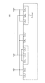
図8は、本発明の一実施形態による表示装置のブロック図である。
図8に示すように、表示装置400は、表示パネル300、メイン印刷回路基板210、第1及び第2データ印刷回路基板220、230、第1及び第2データ駆動部261、262、及び第1及び第2ゲート駆動部271、272を含む。
FIG. 8 is a block diagram of a display device according to an embodiment of the present invention.
As shown in FIG. 8, the
メイン印刷回路基板210上には、第1及び第2電圧発生部110、120、出力タイミング制御部130及びガンマ電圧発生部140が具備される。第1及び第2電圧発生部110、120、出力タイミング制御部130及びガンマ電圧発生部140は、各々別途のチップからなり、メイン印刷回路基板210上に実装され得る。第1及び第2電圧発生部110、120、出力タイミング制御部130及びガンマ電圧発生部140については、図1のところで具体的に説明したので、詳しい説明は省略する。
First and
メイン印刷回路基板210は、フレキシブル回路基板240を通して第1及び第2データ印刷回路基板220、230に電気的に接続される。したがって、出力タイミング制御部130から出力された第3共通電圧AVDD3と、ガンマ電圧発生部140から出力された複数のガンマ電圧VGMMAとは、フレキシブル回路基板240を介して第1及び第2データ印刷回路基板220、230側に伝達される。
The main printed
第1データ印刷回路基板220は、複数の第1テープキャリアパッケージ251を介して表示パネル300に電気的に接続され、第2データ印刷回路基板230は、複数の第2テープキャリアパッケージ252を介して表示パネル300に電気的に接続される。
The first data printed
第1及び第2データ駆動部261、262は、各々複数の第1駆動チップ261a及び複数の第2駆動チップ262aで構成される。複数の第1及び第2駆動チップ261a、262aは、複数の第1及び第2テープキャリアパッケージ251、252上にそれぞれ実装され得る。したがって、複数の第1及び第2駆動チップ261a、262aはメイン印刷回路基板210から出力された第3駆動電圧AVDD3と複数のガンマ電圧VGMMAに応答して動作できる。
Each of the first and second
表示パネル300には、複数のゲートラインGL1〜GLnと複数のデータライン(DL1〜DLm、DLm+1〜DL2m)が具備される。複数のゲートラインGL1〜GLnと複数のデータライン(DL1〜DLm、DLm+1〜DL2m)は互いに直交する方向に延長され、互いに絶縁して交差する。特に、複数のデータライン(DL1〜DLm、DLm+1〜DL2m)は、表示パネル300を左右に二等分する仮想線CLを基準に左側に具備される第1グループDL1〜DLm及び仮想線CLを基準に右側に具備される第2グループDLm+1〜DL2mに区分される。
複数の第1駆動チップ261aは、第1グループDL1〜DLmに電気的に接続され、第1データ信号を印加し、複数の第2駆動チップ262aは、第2グループDLm+1〜DL2mに電気的に接続され、第2データ信号を印加する。
The
The plurality of
一方、複数のゲートラインGL1〜GLnの両端部に隣接して、第1及び第2ゲート駆動部271、272がそれぞれ具備される。第1及び第2ゲート駆動部271、272はメイン印刷回路基板210から供給されたゲートオン電圧及びゲートオフ電圧をそれぞれ受けて、ゲート信号を順次に出力する。第1及び第2ゲート駆動部271、272から出力されたゲート信号はゲートラインの両端部を介して複数のゲートラインGL1〜GLnに順次に印加され得る。
Meanwhile, first and second
表示パネル300には複数のゲートラインGL1〜GLnと複数のデータライン(DL1〜DLm、DLm+1〜DL2m)によってマトリックス状に複数の画素領域が定義され、複数の画素領域には、複数の画素がそれぞれ具備される。各画素は薄膜トランジスタTFT及び液晶キャパシタCLCで構成される。本発明の一例として、一番目の画素P1において、薄膜トランジスタTFTは、第1ゲートラインGL1に接続されたゲート電極と、第1データラインDL1に接続されたソース電極と、液晶キャパシタCLCに接続されたドレイン電極とで構成される。
In the
したがって、薄膜トランジスタTFTはゲート信号に応答して第1データ信号をドレイン電極に出力する。液晶キャパシタCLCはドレイン電極に接続された第1電極、共通電圧を受ける第2電極、及び第1電極と第2電極との間に介在する液晶層(図示せず)で構成される。したがって、液晶キャパシタCLCにはドレイン電極に印加された第1データ信号と共通電圧との電位差に該当する電圧が充電され、充電された電圧の大きさによって液晶層の光透過度が制御される。 Accordingly, the thin film transistor TFT outputs the first data signal to the drain electrode in response to the gate signal. The liquid crystal capacitor CLC includes a first electrode connected to the drain electrode, a second electrode that receives a common voltage, and a liquid crystal layer (not shown) interposed between the first electrode and the second electrode. Accordingly, the liquid crystal capacitor C LC is charged with a voltage corresponding to the potential difference between the first data signal applied to the drain electrode and the common voltage, and the light transmittance of the liquid crystal layer is controlled according to the magnitude of the charged voltage. .
表示パネル300は、表示パネル300の後面又は前面から提供される光の透過度を液晶層によって制御して、表示パネル300の画面上に所望の階調の画像を表示できる。
表示パネル300が大型化すれば、電圧発生部から出力される駆動電圧の出力容量が不足する可能性があるため、上述したようにメイン印刷回路基板210には第1及び第2電圧発生部110、120が具備される。また、第1及び第2電圧発生部110、120から出力される第1及び第2駆動電圧AVDD1、AVDD2の間に時間差が生じ得るので、メイン印刷回路基板210には出力タイミング制御部130がさらに具備され得る。
The
If the
出力タイミング制御部130は、第1及び第2駆動電圧AVDD1、AVDD2を受けて第3駆動電圧AVDD3を第1及び第2データ駆動部261、262に同時に供給する。したがって、第3駆動電圧AVDD3によって、第1及び第2データ駆動部261、262の駆動時点を同期することができ、その結果、仮想線CLを基準に表示パネル300の左右側の画面に画像を同時に表示することができる。
The
また、ガンマ電圧発生部140は、出力タイミング制御部130からの第3駆動電圧AVDD3に基づいて複数のガンマ電圧VGMMAを発生させて、複数のガンマ電圧VGMMAは常に第3駆動電圧AVDD3より後で第1及び第2データ駆動部150、160に印加することができる。したがって、複数のガンマ電圧VGMMAと第3駆動電圧AVDD3間の逆電位現象を防止し、逆電位現象による第1及び第2データ駆動部150、160の損傷を防止できる。
The
尚、本発明は、上述の実施形態に限られるものではない。本発明の技術的範囲から逸脱しない範囲内で多様に変更実施することが可能である。 The present invention is not limited to the embodiment described above. Various modifications can be made without departing from the technical scope of the present invention.
100、190 駆動装置
110 第1電圧発生部
120 第2電圧発生部
130、170 出力タイミング制御部
140 ガンマ電圧発生部
150、261 第1データ駆動部
160、262 第2データ駆動部
180 タイミングコントローラ
210 メイン印刷回路基板
220 第1データ印刷回路基板
230 第2データ印刷回路基板
240 フレキシブル回路基板
251 第1テープキャリアパッケージ
252 第2テープキャリアパッケージ
261a 第1駆動チップ
262a 第2駆動チップ
271 第1ゲート駆動部
272 第2ゲート駆動部
300 表示パネル
400 表示装置
100, 190
Claims (12)
前記電源電圧を受けて第2駆動電圧を出力する第2電圧発生部と、
前記第1及び第2電圧発生部からの前記第1及び第2駆動電圧をそれぞれ受けて、所定の時点で第3駆動電圧を出力する出力タイミング制御部と、
前記出力タイミング制御部から前記第3駆動電圧を受けて複数のガンマ電圧を出力するガンマ電圧発生部と、
前記出力タイミング制御部からの前記第3駆動電圧に応答して動作し、前記ガンマ電圧発生部から供給された前記複数のガンマ電圧に基づいて第1画像信号を第1データ信号に変換する第1データ駆動部と、
前記出力タイミング制御部からの前記第3駆動電圧に応答して動作し、前記ガンマ電圧発生部から供給された前記複数のガンマ電圧に基づいて第2画像信号を第2データ信号に変換する第2データ駆動部と、を有することを特徴とする駆動装置。 A first voltage generator for receiving a power supply voltage from the outside and outputting a first drive voltage;
A second voltage generator for receiving the power supply voltage and outputting a second drive voltage;
An output timing controller that receives the first and second drive voltages from the first and second voltage generators and outputs a third drive voltage at a predetermined time; and
A gamma voltage generator that receives the third drive voltage from the output timing controller and outputs a plurality of gamma voltages;
A first operation is performed in response to the third drive voltage from the output timing control unit, and a first image signal is converted into a first data signal based on the plurality of gamma voltages supplied from the gamma voltage generation unit. A data driver;
The second image signal operates in response to the third driving voltage from the output timing control unit, and converts a second image signal into a second data signal based on the plurality of gamma voltages supplied from the gamma voltage generation unit. And a data drive unit.
前記複数の電圧発生部からの前記複数の駆動電圧を受け、所定の時点でタイミング制御信号に応答して共通駆動電圧を出力する出力タイミング制御部と、
前記出力タイミング制御部からの前記共通駆動電圧を受けて複数のガンマ電圧を出力するガンマ電圧発生部と、
前記出力タイミング制御部からの前記共通駆動電圧に応答して動作し、前記ガンマ電圧発生部から提供された前記複数のガンマ電圧に基づいて画像信号をデータ信号に変換する複数のデータ駆動部と、を有することを特徴とする駆動装置。 A plurality of voltage generators for receiving a power supply voltage from the outside and outputting a plurality of driving voltages respectively;
An output timing controller that receives the plurality of driving voltages from the plurality of voltage generators and outputs a common driving voltage in response to a timing control signal at a predetermined time;
A gamma voltage generator that receives the common drive voltage from the output timing controller and outputs a plurality of gamma voltages;
A plurality of data driving units that operate in response to the common driving voltage from the output timing control unit and convert an image signal into a data signal based on the plurality of gamma voltages provided from the gamma voltage generation unit; A drive device comprising:
前記複数のトランジスタの各々は、前記複数の入力端子のうち対応する入力端子に接続される入力電極と、前記タイミング制御信号を受信する制御電極と、前記複数の出力端子のうち対応する出力端子に接続される出力電極と、を含み、前記タイミング制御信号に応答して前記共通駆動電圧を前記対応する出力端子に出力することを特徴とする請求項3に記載の駆動装置。 The output timing controller includes a plurality of transistors connected between a plurality of input terminals that respectively receive a plurality of drive voltages and a plurality of output terminals that output the common drive voltage,
Each of the plurality of transistors includes an input electrode connected to a corresponding input terminal among the plurality of input terminals, a control electrode receiving the timing control signal, and a corresponding output terminal among the plurality of output terminals. The drive device according to claim 3 , further comprising: an output electrode connected to the output device, wherein the common drive voltage is output to the corresponding output terminal in response to the timing control signal.
前記電源電圧を受けて第2駆動電圧を出力する第2電圧発生部と、
前記第1及び第2電圧発生部からの前記第1及び第2駆動電圧をそれぞれ受けて、所定の時点で第3駆動電圧を出力する出力タイミング制御部と、
前記出力タイミング制御部からの前記第3駆動電圧を受けて複数のガンマ電圧を出力するガンマ電圧発生部と、
前記出力タイミング制御部からの前記第3駆動電圧に応答して動作し、前記ガンマ電圧発生部から供給された前記複数のガンマ電圧に基づいて第1画像信号を第1データ信号に変換する第1データ駆動部と、
前記出力タイミング制御部からの前記第3駆動電圧に応答して動作し、前記ガンマ電圧発生部から供給された前記複数のガンマ電圧に基づいて第2画像信号を第2データ信号に変換する第2データ駆動部と、
前記第1及び第2電圧発生部のうちの何れか一つから出力されたゲートオン電圧及びゲートオフ電圧を受けてゲート信号を順次に出力するゲート駆動部と、
前記ゲート信号に応答して、前記第1及び第2データ信号を受信して画像を表示する表示パネルと、を有することを特徴とする表示装置。 A first voltage generator for receiving a power supply voltage from the outside and outputting a first drive voltage;
A second voltage generator for receiving the power supply voltage and outputting a second drive voltage;
An output timing controller that receives the first and second drive voltages from the first and second voltage generators and outputs a third drive voltage at a predetermined time; and
A gamma voltage generator that receives the third drive voltage from the output timing controller and outputs a plurality of gamma voltages;
A first operation is performed in response to the third drive voltage from the output timing control unit, and a first image signal is converted into a first data signal based on the plurality of gamma voltages supplied from the gamma voltage generation unit. A data driver;
The second image signal operates in response to the third driving voltage from the output timing control unit, and converts a second image signal into a second data signal based on the plurality of gamma voltages supplied from the gamma voltage generation unit. A data driver;
A gate driver that sequentially receives a gate-on voltage and a gate-off voltage output from any one of the first and second voltage generators and outputs a gate signal;
And a display panel for receiving the first and second data signals and displaying an image in response to the gate signal.
前記第1及び第2駆動電圧がすべて“ハイ”状態である時、第3駆動電圧を出力するステップと、
前記第3駆動電圧に応答して複数のガンマ電圧を出力するステップと、
前記第3駆動電圧に応答して第1画像信号を前記複数のガンマ電圧に基づいて第1データ信号に変換するステップと、
前記第3駆動電圧に応答して第2画像信号を前記複数のガンマ電圧に基づいて第2データ信号に変換するステップと、
ゲート信号を順次に出力するステップと、
前記ゲート信号に応答して前記第1及び第2データ信号に対応する画像を表示するステップと、を有し、
前記第1駆動電圧と前記第2駆動電圧は、互いに異なる時間に“ロウ”状態から“ハイ”状態に変化することを特徴とする表示装置の駆動方法。 Receiving a power supply voltage from outside and outputting first and second drive voltages;
Outputting a third drive voltage when all of the first and second drive voltages are in a “high” state;
Outputting a plurality of gamma voltages in response to the third drive voltage;
Converting a first image signal into a first data signal based on the plurality of gamma voltages in response to the third drive voltage;
Converting a second image signal into a second data signal based on the plurality of gamma voltages in response to the third drive voltage;
Sequentially outputting gate signals;
Displaying images corresponding to the first and second data signals in response to the gate signal;
The display device driving method, wherein the first driving voltage and the second driving voltage change from a “low” state to a “high” state at different times.
Applications Claiming Priority (2)
| Application Number | Priority Date | Filing Date | Title |
|---|---|---|---|
| KR10-2007-0073094 | 2007-07-20 | ||
| KR1020070073094A KR101410955B1 (en) | 2007-07-20 | 2007-07-20 | Display apparatus and method of driving the display apparatus |
Publications (3)
| Publication Number | Publication Date |
|---|---|
| JP2009025802A JP2009025802A (en) | 2009-02-05 |
| JP2009025802A5 JP2009025802A5 (en) | 2011-07-07 |
| JP5268054B2 true JP5268054B2 (en) | 2013-08-21 |
Family
ID=39816943
Family Applications (1)
| Application Number | Title | Priority Date | Filing Date |
|---|---|---|---|
| JP2008144538A Active JP5268054B2 (en) | 2007-07-20 | 2008-06-02 | Driving device, display device having the same, and driving method thereof |
Country Status (6)
| Country | Link |
|---|---|
| US (2) | US8379011B2 (en) |
| EP (1) | EP2017815B1 (en) |
| JP (1) | JP5268054B2 (en) |
| KR (1) | KR101410955B1 (en) |
| CN (1) | CN101350180A (en) |
| TW (1) | TWI452556B (en) |
Families Citing this family (19)
| Publication number | Priority date | Publication date | Assignee | Title |
|---|---|---|---|---|
| WO2010051485A1 (en) * | 2008-10-31 | 2010-05-06 | Medtronic Inc | Interference mitigation for implantable device recharging |
| US8284147B2 (en) * | 2008-12-29 | 2012-10-09 | Himax Technologies Limited | Source driver, display device using the same and driving method of source driver |
| TWI409781B (en) * | 2009-03-26 | 2013-09-21 | Himax Tech Ltd | Source driver, display device using the same and driving method of source driver |
| TWI418970B (en) * | 2010-01-20 | 2013-12-11 | Novatek Microelectronics Corp | Silicon intellectual property architecture capable of adjusting control timing and related driving chip |
| US8537043B1 (en) * | 2012-04-12 | 2013-09-17 | Analog Devices, Inc. | Digital-to-analog converter with controlled gate voltages |
| TWI464731B (en) | 2012-09-20 | 2014-12-11 | Au Optronics Corp | Display-driving structure and signal transmission method thereof, displaying device and manufacturing method thereof |
| DE102013211850A1 (en) * | 2013-06-21 | 2014-12-24 | Gilupi Gmbh | Rapid test for detection of pathogen material, in particular to support the diagnosis of sepsis, and kit and device for performing a sepsis test |
| KR20160062372A (en) | 2014-11-25 | 2016-06-02 | 삼성디스플레이 주식회사 | Data driving device and display device having the same |
| KR102331176B1 (en) | 2015-06-11 | 2021-11-26 | 삼성디스플레이 주식회사 | Display Device |
| JP6543522B2 (en) * | 2015-07-06 | 2019-07-10 | 株式会社ジャパンディスプレイ | Display device |
| KR102513369B1 (en) * | 2015-09-22 | 2023-03-24 | 삼성디스플레이 주식회사 | Display panel driving apparatus, method of driving display panel using the same and display apparatus having the same |
| CN105161070A (en) * | 2015-10-30 | 2015-12-16 | 京东方科技集团股份有限公司 | Driving circuit used for display panel and display device |
| CN105632445B (en) * | 2016-03-17 | 2018-11-27 | 武汉华星光电技术有限公司 | Display driver circuit and display panel |
| KR102526613B1 (en) * | 2016-07-29 | 2023-04-28 | 엘지디스플레이 주식회사 | Display Device and Method of Driving the same |
| KR102517759B1 (en) * | 2016-08-31 | 2023-04-03 | 엘지디스플레이 주식회사 | Power supply unit and display device including the same |
| CN107068101B (en) * | 2017-05-22 | 2018-05-18 | 惠科股份有限公司 | Driving circuit and driving method of display device and display device |
| CN107680555B (en) * | 2017-11-22 | 2020-07-31 | 深圳市华星光电技术有限公司 | Drive circuit board of liquid crystal display panel and liquid crystal display device |
| CN111798757A (en) * | 2020-07-10 | 2020-10-20 | Tcl华星光电技术有限公司 | Display panel and display device |
| CN112687221B (en) * | 2020-12-24 | 2024-04-05 | 厦门天马微电子有限公司 | Display module and display device |
Family Cites Families (20)
| Publication number | Priority date | Publication date | Assignee | Title |
|---|---|---|---|---|
| US3464036A (en) * | 1966-02-07 | 1969-08-26 | Mc Graw Edison Co | R.f. attenuator with electronic switching |
| JPH08334743A (en) * | 1995-06-07 | 1996-12-17 | Hitachi Ltd | Liquid crystal display device |
| KR0176429B1 (en) * | 1996-02-28 | 1999-04-01 | 윤종용 | DC shock prevention method of LCD module |
| KR100237685B1 (en) * | 1997-09-09 | 2000-01-15 | 윤종용 | Liquid crystal display device with electric power control circuit |
| TW407256B (en) | 1998-10-16 | 2000-10-01 | Samsung Electronics Co Ltd | Power supply apparatus of an LCD and voltage sequence control method |
| JP2000322018A (en) | 1999-05-10 | 2000-11-24 | Sharp Corp | Display device |
| KR100843685B1 (en) * | 2001-12-27 | 2008-07-04 | 엘지디스플레이 주식회사 | Method and apparatus for driving liquid crystal display |
| JP2003202837A (en) | 2001-12-28 | 2003-07-18 | Pioneer Electronic Corp | Device and method for driving display panel |
| KR20050018287A (en) | 2003-08-16 | 2005-02-23 | 삼성전자주식회사 | Driving IC of Liquid Crystal Display |
| KR100998119B1 (en) | 2003-12-02 | 2010-12-02 | 엘지디스플레이 주식회사 | Liquid crystal display |
| KR100982121B1 (en) * | 2003-12-23 | 2010-09-14 | 엘지디스플레이 주식회사 | Liquid Crysyal Display And Driving Method Thereof |
| KR100983712B1 (en) | 2003-12-30 | 2010-09-24 | 엘지디스플레이 주식회사 | Unit of driving liquid crystal display |
| KR20060020074A (en) | 2004-08-31 | 2006-03-06 | 삼성전자주식회사 | Display apparatus |
| KR101096712B1 (en) * | 2004-12-28 | 2011-12-22 | 엘지디스플레이 주식회사 | A liquid crystal display device and a method for the same |
| TWI277793B (en) | 2005-05-10 | 2007-04-01 | Novatek Microelectronics Corp | Source driving device and timing control method thereof |
| KR101154341B1 (en) * | 2005-08-03 | 2012-06-13 | 삼성전자주식회사 | Display device, method and apparatus for driving the same |
| KR101123716B1 (en) * | 2005-09-16 | 2012-03-15 | 삼성전자주식회사 | Display apparatus and control method thereof |
| KR101197057B1 (en) * | 2005-12-12 | 2012-11-06 | 삼성디스플레이 주식회사 | Display device |
| KR101231840B1 (en) * | 2005-12-28 | 2013-02-08 | 엘지디스플레이 주식회사 | Liquid crystal display and method for driving the same |
| KR20070080623A (en) * | 2006-02-08 | 2007-08-13 | 삼성전자주식회사 | Gamma voltage generating apparatus and display device having the same |
-
2007
- 2007-07-20 KR KR1020070073094A patent/KR101410955B1/en active IP Right Grant
-
2008
- 2008-03-29 EP EP08006204.5A patent/EP2017815B1/en active Active
- 2008-06-02 JP JP2008144538A patent/JP5268054B2/en active Active
- 2008-06-25 US US12/145,825 patent/US8379011B2/en active Active
- 2008-07-03 TW TW097125058A patent/TWI452556B/en active
- 2008-07-17 CN CNA2008101338433A patent/CN101350180A/en active Pending
-
2012
- 2012-11-30 US US13/691,029 patent/US8723853B2/en active Active
Also Published As
| Publication number | Publication date |
|---|---|
| EP2017815B1 (en) | 2018-03-07 |
| US8723853B2 (en) | 2014-05-13 |
| KR101410955B1 (en) | 2014-07-03 |
| EP2017815A2 (en) | 2009-01-21 |
| TW200912841A (en) | 2009-03-16 |
| US8379011B2 (en) | 2013-02-19 |
| JP2009025802A (en) | 2009-02-05 |
| EP2017815A3 (en) | 2011-05-11 |
| US20090021507A1 (en) | 2009-01-22 |
| US20130088478A1 (en) | 2013-04-11 |
| TWI452556B (en) | 2014-09-11 |
| CN101350180A (en) | 2009-01-21 |
| KR20090009640A (en) | 2009-01-23 |
Similar Documents
| Publication | Publication Date | Title |
|---|---|---|
| JP5268054B2 (en) | Driving device, display device having the same, and driving method thereof | |
| US9230496B2 (en) | Display device and method of driving the same | |
| KR101260838B1 (en) | Liquid crystal display device | |
| JP2004094014A (en) | Display device | |
| KR102455584B1 (en) | Organic Light Emitting Diode display panel and Organic Light Emitting Diode display device using the same | |
| JP2012047894A (en) | Display device | |
| KR101942984B1 (en) | Gate driver and image display device including the same | |
| KR102203773B1 (en) | Display panel and Organic Light Emitting Diode display device using the same | |
| KR102379188B1 (en) | Display device and driving method of the same | |
| KR20090054205A (en) | Liquid crystal display | |
| KR20220089884A (en) | Residual charge processing display apparatus | |
| KR20160083565A (en) | Display Device | |
| KR102238637B1 (en) | Display Device | |
| US10304406B2 (en) | Display apparatus with reduced flash noise, and a method of driving the display apparatus | |
| KR101785339B1 (en) | Common voltage driver and liquid crystal display device including thereof | |
| US20180061319A1 (en) | Display device and controller | |
| KR102674253B1 (en) | Display device | |
| JP7300496B2 (en) | Display device including multiplexer | |
| JP2014098863A (en) | Display device and display method | |
| KR20170140624A (en) | Display Device Including Power Supplying Part | |
| KR20170051777A (en) | Gate driver, display panel and display device | |
| KR101953173B1 (en) | Organic light emitting decvice | |
| KR101968204B1 (en) | Liquid crystal display device and method of driving the same | |
| TWI567720B (en) | Image display device and method for manufacturing the same | |
| KR20200058893A (en) | Display Device And Method Of Driving The Same |
Legal Events
| Date | Code | Title | Description |
|---|---|---|---|
| A521 | Request for written amendment filed |
Free format text: JAPANESE INTERMEDIATE CODE: A523 Effective date: 20110523 |
|
| A621 | Written request for application examination |
Free format text: JAPANESE INTERMEDIATE CODE: A621 Effective date: 20110523 |
|
| A521 | Request for written amendment filed |
Free format text: JAPANESE INTERMEDIATE CODE: A523 Effective date: 20120522 |
|
| A977 | Report on retrieval |
Free format text: JAPANESE INTERMEDIATE CODE: A971007 Effective date: 20121031 |
|
| A711 | Notification of change in applicant |
Free format text: JAPANESE INTERMEDIATE CODE: A712 Effective date: 20121213 |
|
| TRDD | Decision of grant or rejection written | ||
| A01 | Written decision to grant a patent or to grant a registration (utility model) |
Free format text: JAPANESE INTERMEDIATE CODE: A01 Effective date: 20130416 |
|
| A61 | First payment of annual fees (during grant procedure) |
Free format text: JAPANESE INTERMEDIATE CODE: A61 Effective date: 20130430 |
|
| R150 | Certificate of patent or registration of utility model |
Free format text: JAPANESE INTERMEDIATE CODE: R150 Ref document number: 5268054 Country of ref document: JP Free format text: JAPANESE INTERMEDIATE CODE: R150 |
|
| R250 | Receipt of annual fees |
Free format text: JAPANESE INTERMEDIATE CODE: R250 |
|
| R250 | Receipt of annual fees |
Free format text: JAPANESE INTERMEDIATE CODE: R250 |
|
| R250 | Receipt of annual fees |
Free format text: JAPANESE INTERMEDIATE CODE: R250 |
|
| R250 | Receipt of annual fees |
Free format text: JAPANESE INTERMEDIATE CODE: R250 |
|
| R250 | Receipt of annual fees |
Free format text: JAPANESE INTERMEDIATE CODE: R250 |
|
| R250 | Receipt of annual fees |
Free format text: JAPANESE INTERMEDIATE CODE: R250 |
|
| R250 | Receipt of annual fees |
Free format text: JAPANESE INTERMEDIATE CODE: R250 |
|
| R250 | Receipt of annual fees |
Free format text: JAPANESE INTERMEDIATE CODE: R250 |
|
| R250 | Receipt of annual fees |
Free format text: JAPANESE INTERMEDIATE CODE: R250 |