JP5259678B2 - Single pole multi throw switch - Google Patents
Single pole multi throw switch Download PDFInfo
- Publication number
- JP5259678B2 JP5259678B2 JP2010244873A JP2010244873A JP5259678B2 JP 5259678 B2 JP5259678 B2 JP 5259678B2 JP 2010244873 A JP2010244873 A JP 2010244873A JP 2010244873 A JP2010244873 A JP 2010244873A JP 5259678 B2 JP5259678 B2 JP 5259678B2
- Authority
- JP
- Japan
- Prior art keywords
- switching unit
- unit
- switching
- coupled
- common port
- Prior art date
- Legal status (The legal status is an assumption and is not a legal conclusion. Google has not performed a legal analysis and makes no representation as to the accuracy of the status listed.)
- Active
Links
- 230000003071 parasitic effect Effects 0.000 claims description 54
- 230000005540 biological transmission Effects 0.000 claims description 11
- 238000000034 method Methods 0.000 claims description 11
- 230000003213 activating effect Effects 0.000 claims description 3
- 239000003990 capacitor Substances 0.000 description 9
- 238000010586 diagram Methods 0.000 description 9
- 238000003780 insertion Methods 0.000 description 8
- 230000037431 insertion Effects 0.000 description 8
- 239000004065 semiconductor Substances 0.000 description 4
- 101100532456 Rattus norvegicus Slc28a2 gene Proteins 0.000 description 3
- 230000001413 cellular effect Effects 0.000 description 3
- 229910044991 metal oxide Inorganic materials 0.000 description 3
- 150000004706 metal oxides Chemical class 0.000 description 3
- 230000000295 complement effect Effects 0.000 description 2
- 230000000694 effects Effects 0.000 description 2
- 238000002955 isolation Methods 0.000 description 2
- 230000008569 process Effects 0.000 description 2
- 230000004913 activation Effects 0.000 description 1
- 230000008901 benefit Effects 0.000 description 1
- 230000015556 catabolic process Effects 0.000 description 1
- 238000004891 communication Methods 0.000 description 1
- 230000009849 deactivation Effects 0.000 description 1
- 238000005516 engineering process Methods 0.000 description 1
- 238000010295 mobile communication Methods 0.000 description 1
- 238000012545 processing Methods 0.000 description 1
- 230000009467 reduction Effects 0.000 description 1
- 238000012552 review Methods 0.000 description 1
Images
Classifications
-
- H—ELECTRICITY
- H01—ELECTRIC ELEMENTS
- H01P—WAVEGUIDES; RESONATORS, LINES, OR OTHER DEVICES OF THE WAVEGUIDE TYPE
- H01P1/00—Auxiliary devices
- H01P1/10—Auxiliary devices for switching or interrupting
- H01P1/15—Auxiliary devices for switching or interrupting by semiconductor devices
-
- H—ELECTRICITY
- H03—ELECTRONIC CIRCUITRY
- H03K—PULSE TECHNIQUE
- H03K17/00—Electronic switching or gating, i.e. not by contact-making and –breaking
- H03K17/51—Electronic switching or gating, i.e. not by contact-making and –breaking characterised by the components used
- H03K17/56—Electronic switching or gating, i.e. not by contact-making and –breaking characterised by the components used by the use, as active elements, of semiconductor devices
- H03K17/687—Electronic switching or gating, i.e. not by contact-making and –breaking characterised by the components used by the use, as active elements, of semiconductor devices the devices being field-effect transistors
- H03K17/693—Switching arrangements with several input- or output-terminals, e.g. multiplexers, distributors
Landscapes
- Electronic Switches (AREA)
- Transceivers (AREA)
- Waveguide Switches, Polarizers, And Phase Shifters (AREA)
Description
単極N投無線周波(RF)スイッチでは、挿入損失が、切り替えアクティブ要素(例えば、CMOSトランジスタ、相補形金属膜酸化半導体トランジスタ)のオン抵抗により低減し、ポート間絶縁を改良するために使用されるオフポートシャントの抵抗の1/(N−1)に直列するオフポートの寄生容量の(N−1)倍だけ低減する。抵抗を、シャントのサイズ(例えば、長さまたは幅)を増大させることにより低減することができ、静電容量は外部LC整合回路網により整合される。アンテナ切り替え用途の場合、例えば、ESD保護および低周波数帯域での寄生容量の補償のために並列インダクタが追加される一方で、直列インダクタ−並列キャパシタ回路網が高帯域整合に使用される。 In single-pole N-throw radio frequency (RF) switches, insertion loss is reduced by the on-resistance of switching active elements (eg, CMOS transistors, complementary metal oxide semiconductor transistors) and used to improve inter-port isolation. The resistance of the off-port shunt is reduced by (N-1) times the parasitic capacitance of the off-port in series with 1 / (N-1). The resistance can be reduced by increasing the size (eg, length or width) of the shunt and the capacitance is matched by an external LC matching network. For antenna switching applications, for example, a parallel inductor is added for ESD protection and parasitic capacitance compensation in the low frequency band, while a series inductor-parallel capacitor network is used for high band matching.
既知のスイッチのいくつかは、挿入損失が高いという欠点を有する。既知のスイッチの他のいくつかは、離散要素または外部構成要素が多いという欠点を有する。 Some known switches have the disadvantage of high insertion loss. Some other known switches have the disadvantage that there are many discrete or external components.
様々な態様が本明細書に開示される。例えば、いくつかの態様は単極多投スイッチに関する。このスイッチは、第1の切り替えユニットと、共通ポートに結合され、オフ状態寄生静電容量を備える第2の切り替えユニットと、整合ユニットとを備え得る。整合ユニットは、第1の切り替えユニットと共通ポートとの間に結合することができ、整合ユニットは、第1の切り替えユニットがアクティブであり、第2の切り替えユニットが非アクティブである場合、第2の切り替えユニットのオフ状態寄生静電容量と併せて、インピーダンス整合に寄与するように構成される。 Various aspects are disclosed herein. For example, some aspects relate to single pole multiple throw switches. The switch may comprise a first switching unit, a second switching unit coupled to the common port and having an off-state parasitic capacitance, and a matching unit. The matching unit can be coupled between the first switching unit and the common port, and the matching unit can be configured as a second if the first switching unit is active and the second switching unit is inactive. Together with the off-state parasitic capacitance of the switching unit, the switching unit is configured to contribute to impedance matching.
本開示のこれらおよび他の態様は、以下の詳細な説明の検討から明らかになるであろう。 These and other aspects of the disclosure will become apparent from a review of the following detailed description.
例示的な様々な実施形態について、添付図を参照して以下にさらに詳細に説明する。 Various exemplary embodiments are described in further detail below with reference to the accompanying drawings.
以下では、同じ参照番号が部分的に、同じまたは同様の機能特性を有する機能ユニットおよび他の要素に使用され、1つの図に関する記述は実施形態の説明の冗長性を低減するために他の図にも当てはまる。 In the following, the same reference numerals will be used in part for functional units and other elements having the same or similar functional characteristics , and the description with respect to one figure will be reduced to other figures in order to reduce the redundancy of the description of the embodiments . Also applies.
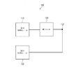
図1は、例示的な実施形態による単極多投スイッチ100のブロック図を示す。単極多投スイッチ100は、第1の切り替えユニット110、第2の切り替えユニット120、および整合ユニット130を備える。第2の切り替えユニット120は、共通ポート102に結合され、オフ状態寄生静電容量を備える。整合ユニット130は、第1の切り替えユニット110と共通ポート102との間に電気的に結合される。さらに、整合ユニット130は、第1の切り替えユニット110がアクティブであり、第2の切り替えユニット120が非アクティブの場合、第2の切り替えユニット120のオフ状態寄生静電容量と併せて、インピーダンス整合に寄与するように構成される。
FIG. 1 shows a block diagram of a single pole
2つの別個の切り替えユニットを有する単極多投スイッチ100を実施し、第1の切り替えユニット110の出力整合のために第2の切り替えユニット120のオフ状態寄生静電容量を使用することにより、スイッチ100の挿入損失を大幅に低減することができる。さらに、インピーダンス整合する整合ユニット130の共通ポート側で有効な第2の切り替えユニット120のオフ状態寄生静電容量を使用することにより、例えば、整合ユニット130の一部としてインピーダンス整合に従来必要な整合キャパシタがもはや必要なくなり得る。このようにして、スイッチの要素または外部構成要素の数を低減し得る。スイッチの要素数の低減により、スイッチのコストも低減し得る。さらに、第1の切り替えユニット110(または第1の切り替えユニットを通る経路)および/または第2の切り替えユニット120(または第2の切り替えユニットを通る経路)に対する(例えば、共通ポートでの)インピーダンス整合を改良させ得る。
By implementing a single pole
単極多投スイッチ100の単極は、共通ポート102で表される。さらに、各切り替えユニット110、120は、共通ポート102に提供される信号を受信するか、または共通ポート102から受信される信号を提供する、スイッチ100の「投」ポートに結合された少なくとも1つの入力端子および/または出力端子を備える。
A single pole of the single-pole
共通ポート102は、例えば、信号を受信または送信するアンテナまたは伝送線に結合し得る。
The
整合ユニット130は、第1の切り替えユニット110がアクティブな場合、共通ポート102から第1の切り替えユニット110に、または第1の切り替えユニット110から共通ポート102に流れる信号に対するインピーダンスを整合させるためオフ状態寄生静電容量を利用するように構成され得る。換言すれば、整合ユニット130は、まるで、第2の切り替えユニット120のオフ状態寄生静電容量が整合ユニット130の要素または構成要素であるかのように設計され得る。
The matching
第1の切り替えユニット110および第2の切り替えユニット120はそれぞれ、少なくとも1つの信号経路を備える。切り替えユニットの信号経路がオンに切り替えられると、切り替えユニットを通って共通ポート102から切り替えユニットの出力に、または切り替えユニットの入力から共通ポート102に信号が通ることができるように、切り替えユニットはアクティブである。当然ながら、切り替えユニットの「投」ポートは入力/出力ポートであり得るように、切り替えユニットは双方向であり得る。他方、切り替えユニットは、切り替えユニットの信号経路がオンに切り替えられず、信号が切り替えユニットを通ることができない場合、非アクティブである。
Each of the
整合ユニット130は、第1の切り替えユニットがアクティブである場合、第2の切り替えユニット120のオフ状態寄生静電容量と併せて、インピーダンス整合に寄与する。これは、例えば、第1の切り替えユニット110を通る(例えば、第1の切り替えユニットの「投」ポートから共通ポートに向かう)信号の反射を、整合ユニット130を有さないスイッチと比較して低減し得る。
The matching
さらに、整合ユニット130は、第1の切り替えユニット110が非アクティブであり、第2の切り替えユニット120がアクティブな場合、インピーダンス整合に寄与し得る。換言すれば、整合ユニット130は、第2の切り替えユニット120を通る(例えば、第2の切り替えユニットの「投」ポートから共通ポートに向かう)信号の反射を低減することもできる。
Furthermore, the matching
第1の切り替えユニット110もオフ状態寄生静電容量を備えるが、第2の切り替えユニット120を通る信号のインピーダンス整合に対する第1の切り替えユニット110のオフ状態寄生静電容量の影響は、第1の切り替えユニット110を通る信号のインピーダンス整合に対する第2の切り替えユニット120のオフ状態寄生静電容量の影響よりも低い。その理由は、第1の切り替えユニット110が整合ユニット130を通して共通ポート102に結合される一方で、第2の切り替えユニット120は、好ましくは、(例えば、いかなる集中要素も介在させずに)共通ポートに直接結合されるためである。これは、第2の切り替えユニット120を通る信号に対する第1の切り替えユニット110のオフ状態寄生静電容量の影響を低減し得る。換言すれば、整合ユニット130は、第2の切り替えユニットがアクティブである場合、インピーダンス整合に対する第1の切り替えユニット110のオフ状態寄生静電容量の寄与が、第1の切り替えユニット110がアクティブな場合、インピーダンス整合に対する第2の切り替えユニット120のオフ状態寄生静電容量の寄与よりも低くなるように構成される。
Although the
いくつかの実施形態では、第2の切り替えユニット120は共通ポート102に直接接続される。この場合、「直接接続」は、共通ポート102と第2の切り替えユニット120との結合が、ワイヤまたは他の単なる半導体のみにより実現されることを意味する。例えば、インダクタまたは静電容量として別個の要素が、第2の切り替えユニット120と共通ポート102との間(例えば、第2の切り替えユニットの切り替え装置と共通ポートとの間)に電気的に結合されない。換言すれば、例えば、接続線のインダクタンスを考えると、第2の切り替えユニット120と共通ポート102との電気接続は通常、整合ユニット130を通る第1の切り替えユニット110から共通ポート102までの電気経路のインダクタンスの10%未満(または0.1%未満、1%未満、5%未満、20%未満、50%未満)のインダクタンスを備える。
In some embodiments, the
単極多投スイッチ100は、第1の切り替えユニット110を使用して高周波信号を切り替え、第2の切り替えユニット120を使用して低周波信号を切り替えるために使用し得る。換言すれば、スイッチ100は、共通ポート102において異なる周波数の信号を(同時に、または順次)受信または提供し得る。これら信号のうちのいくつかは、他方の信号よりも高い周波数を備える。したがって、信号を高周波信号および低周波信号に分けることができ、低周波と高周波との境目は特定の用途に適合し得る。例えば、携帯電話またはセルラハンドセット用途では、1GHz未満の周波数を有する信号は「低周波信号」と定義され、1GHzよりも高い周波数を有する信号は「高周波信号」と定義され得る。したがって、第1の切り替えユニット110を通る共通ポート102からの信号経路のインピーダンス整合は、第2の切り替えユニット120により切り替えられる信号よりも高い周波数を有する信号に対して、整合ユニット130により改良させることができる。換言すれば、単極多投スイッチ100は、少なくとも1つの低周波信号および少なくとも1つの高周波信号を切り替え可能であり得、整合ユニット130は、第1の切り替えユニット110により切り替えられた場合の高周波に対する整合ユニット130により行われるインピーダンス整合のほうが、第2の切り替えユニット120により切り替えられる場合の高周波信号に対するインピーダンス整合よりも良好なように設計され得る。さらに換言すれば、整合ユニットは、第1の切り替えユニット110を通る信号経路が、第1の周波数を有する信号のプリセットインピーダンス整合を達成し、第2の切り替えユニット120を通る信号経路が、第1の周波数の50%(または80%、30%、10%、1%)未満の第2の周波数を有する信号に対してさえもプリセットインピーダンス整合を達成しないように構成され得る。さらに、共通ポート102から第2の切り替えユニット120を通る信号経路のインピーダンス整合は、第1の切り替えユニット110により切り替えられる信号よりも低い周波数を有する信号に対して整合ユニット130により改良し得る。換言すれば、整合ユニット130は、場合によっては、第2の切り替えユニット120により切り替えられた場合の低周波信号に対して整合ユニット130によって行われるインピーダンス整合のほうが、第1の切り替えユニット110により切り替えられた場合の低周波信号に対するインピーダンス整合よりも良好であるように設計され得る。
The single pole
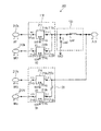
図2は、例示的な実施形態による単極多投スイッチ200のブロック図を示す。単極多投スイッチ200は、図1に示される概念のより詳細な例を示す。この例では、各切り替えユニット110、120は、少なくとも2つの信号経路216a、b、216c、dを備え、各信号経路216a−216bは各自のポート212a−212d(ポートRF1、RF2、RF3、RFn)に結合され、切り替え装置214を備える。
FIG. 2 shows a block diagram of a single pole
図2では、共通ポート102は入力として示され、切り替えユニット110、120の信号経路216a〜216dのポート212a〜212dは、共通ポート102において受信される信号の出力として示される。あるいは、切り替えユニットの信号経路216a〜216dのポート212a〜212dを入力として定義し、共通ポート102を、共通ポート102において提供される信号の出力として定義し得る。共通ポート102および切り替えユニットの信号経路216a〜216dのポート212a〜212dは、共通ポート102において信号を受信および提供する入力および出力として使用してもよい。したがって、単極多投スイッチ200は、受信器、送信器、または送受信器に使用し得る。以下において、スイッチは共通ポート102での信号の受信および/または提供に使用し得るため、入力として示される端子は、出力または入出力端子とでもあり得る。
In FIG. 2, the
各切り替え装置214は、整合ユニット130に結合された第1の端子と、共通ポート102に提供される信号を受信し、または共通ポート102から受信した信号を提供する対応する信号経路216のポートに結合された第2の端子とを備える。さらに、各切り替え装置214は、制御信号を受信する制御入力を備える。制御信号は、切り替え装置214のアクティブ化または非アクティブ化に関して切り替え装置214を制御し得る。
Each
切り替え装置214は、例えば、トランジスタ、中継器、または微小機械スイッチを含み得る。
The
単極多投スイッチ200を使用して、切り替えユニットの異なるポート212a〜212dにおいて異なる周波数範囲の信号を提供(または、送信)し、および/または受信し得る。上述した例によれば、第1の切り替えユニット110のポート212a、bは、第2の切り替えユニット120のポート212c、dにおいて受信または提供される信号の周波数よりも高い周波数を有する信号を受信または提供し得る。換言すれば、第1の切り替えユニット110のポート212a、bは、比較的高い周波数を有する信号を提供または処理するように構成された信号源または信号ドレインに結合し得、第2の切り替えユニット120のポート212c、212dは、比較的低い周波数を有する信号を提供または処理するように構成された信号源または信号ドレインに結合し得る。そのような用途の場合、整合ユニット130が、高周波信号(第1の切り替えユニット110のポート212a、bにおいて受信または提供される信号)のインピーダンス整合を改良し得るように設計され得る。アンテナに結合された共通ポートに結合されたスイッチの場合、異なる周波数を有する複数の信号を切り替えユニットのポート212a〜dにおいて受信かつ提供し得、比較的高い周波数を有する信号は、上述したインピーダンス整合により、第2の切り替えユニット120よりも第1の切り替えユニット110からのほうがより良好な品質で提供し得る。さらに、整合ユニット130は、低周波信号(第2の切り替えユニット120のポート212c、dにおいて提供または受信される信号)のインピーダンス整合も改良するように設計され得る。
Single pole
図2に示される例では、整合ユニット130は、直列インダクタLserおよび並列インダクタLesdを備える。直列インダクタLserは、共通ポート102に結合される第1の端子と、第1の切り替えユニット110の各切り替え装置に(例えば、直接)結合される第2の端子とを備える。並列インダクタンスLesdは、基準電位供給(例えば、接地、GND、0V)に結合される第1の端子と、第1の切り替えユニット110と直列インダクタLserとの間のノードに電気的に結合される第2の端子とを備える。この例では、整合ユニット130は、第2の切り替えユニット120のオフ状態寄生静電容量と組み合わせて、インピーダンス整合に寄与するインダクタ−静電容量整合回路網(L−C回路網)を表す。インピーダンス整合に第2の切り替えユニット120のオフ状態寄生静電容量を使用することにより、L−C回路網の追加キャパシタは必要ない。したがって、既知のスイッチと比較して、スイッチの構成要素数を低減し得る。
In the example shown in FIG. 2, the
あるいは、並列インダクタLesdの第2の端子を、第1の切り替えユニット110と直列インダクタLserとの間のノードではなく、共通ポート102に電気的に結合してもよい。
Alternatively, the second terminal of the parallel inductor Lesd may be electrically coupled to the
別の例では、図2に示されるインダクタ構成が好ましいが、直列インダクタLserおよび/または並列インダクタLesdをキャパシタおよび/または抵抗で置換し得る。 In another example, the inductor configuration shown in FIG. 2 is preferred, but the series inductor Lser and / or the parallel inductor Lesd may be replaced with capacitors and / or resistors.
インピーダンス整合への寄与に加えて、並列インダクタLesdをESD(静電気放電)保護に使用し得る。 In addition to contributing to impedance matching, the parallel inductor Lesd can be used for ESD (electrostatic discharge) protection.
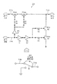
図3は、切り替え装置214を表す電気回路の概略図を示し、トランジスタN1〜N4をバイアスするため存在しても、または存在しなくてもよいバイアス回路は、簡明化のために省かれている。図3に示される切り替え装置214は、図2に示される単極多投スイッチ内に実装される切り替え装置の一例であり、単極単投スイッチ(SPSTスイッチ)と呼ぶこともできる。切り替えユニット214は、(整合ユニット130の横にある第1の切り替えユニット110が、共通ポート102から離れている場合、および整合ユニット130の横にある第2の切り替えユニット120が、共通ポート102に結合されている場合)整合ユニットに結合される入力ポート214aと、切り替え装置の対応する信号経路のポートに結合される出力ポート214bと、制御信号を受信する制御ポート214cとを備える。
FIG. 3 shows a schematic diagram of an electrical circuit representing the
図3の例に関して示されるように、切り替え装置は複数の直列トランジスタを備え得、直列トランジスタのすべてのゲートは、切り替え装置の制御入力に結合される。さらに、複数の直列トランジスタのうちの第1のトランジスタは、切り替え装置の第1の端子に結合され、複数の直列トランジスタのうちの最後のトランジスタは、切り替え装置の第2の端子に結合される。 As shown with respect to the example of FIG. 3, the switching device may comprise a plurality of series transistors, all gates of which are coupled to the control input of the switching device. Further, a first transistor of the plurality of series transistors is coupled to the first terminal of the switching device, and a last transistor of the plurality of series transistors is coupled to the second terminal of the switching device.
図3に示される例は、直列の2つの切り替えトランジスタ(N3、N4)およびシャントトランジスタ(N1、N2)を有するSPSTブロックを示す。直列するオントランジスタおよびシャントトランジスタ(例えば、高周波金属酸化膜半導体トランジスタ、hfmos)の数は、異なる切り替え電力および整合の場合に様々であり得る。ドライバD1およびD2は、例えば、スイッチの切り替えに使用される論理信号(ドライバD2に対してインバータI1により反転し得る)を正電圧に変換して、対応するトランジスタをオンにするか、または負電圧(または0V)に変換して、トランジスタをオフに切り替える。例えば、導電状態(SPSTブロック214のオン状態)では、N1およびN2はオフ(D2出力が負電圧または0V)であり、N3および図4はオン(D1出力が正電圧)である。制御電圧は、積層トランジスタ数ひいてはIC面積を最低限に抑えるために、破壊限界に近いものを選択し得る。ゲート抵抗R1〜R4は、切り替えトランジスタのゲート間の不十分なRF絶縁および低出力インピーダンスゲートドライバによる追加の損失およびひずみを回避するために、高値を有し得る。電力処理能力Pmaxは、例えば、制御電圧Vc、閾値電圧Vth、システムインピーダンスZo、および積層トランジスタ数nに依存する。

図3に示される切り替え装置は、CMOS SPST RFスイッチ(双補形金属酸化膜半導体単極単投無線周波スイッチ)構築ブロックであり得る。 The switching device shown in FIG. 3 may be a CMOS SPST RF switch (double complementary metal oxide semiconductor single pole single throw radio frequency switch) building block.
以下に、本発明による概念の可能な用途について説明する。例えば、特に、セルラ電話分野において規定される通信規格の数の上昇により、6つ以上の異なる帯域を切り替える需要が増大した。同時に、単一PA(電力増幅器)概念および複数受信器が使用されるにつれ、システム部品表内のスイッチの総数(または相対的な総数)が増大する。例えば、単極多投スイッチは、共通ポート(例えば、アンテナポート)と各切り替え(RF)ポートとの間の1つ以上の切り替え要素または切り替え装置(「オントランジスタ」)(例として、CMOSまたはPHEMTトランジスタ、シュードモルフィック高電子移動度トランジスタ)および各切り替えポートとRF接地との間の切り替え要素(「シャントトランジスタ」)により実施し得る。切り替え要素は、オフ状態でかなりの寄生容量を有し、オン状態では有限抵抗を有するため、例えば、寄生低Q容量の値は、切り替えるべきRFポートの数に伴って急激に増大する。高電力信号の場合、寄生容量を直列のトランジスタの数により数分の1減少させるために、より多数の切り替えトランジスタが直列に結合されるが、挿入損失を低減するための非常に大きなトランジスタ幅による寄生容量の増大のほうがより大きいため、性能はスイッチサイズに伴って低減する。RFスイッチ、特にオン抵抗(Ron)および切り替え要素のノード間の寄生容量(Coff)の構築に使用される技術は、性能向上の鍵である。積Ron*Coffは、性能指数として使用し得る。ZoインピーダンスシステムでのnポートSPnTスイッチ(単極多投スイッチ)の挿入損失は、
である。
In the following, possible uses of the concept according to the invention will be described. For example, the demand for switching between six or more different bands has increased, especially with the increase in the number of communication standards defined in the cellular telephone field. At the same time, as single PA (power amplifier) concepts and multiple receivers are used, the total number of switches in the system parts in the table (or relative total) increases. For example, a single pole multiple throw switch may include one or more switching elements or switching devices (“on-transistors”) between a common port (eg, antenna port) and each switching (RF) port (eg, CMOS or PHEMT Transistors, pseudomorphic high electron mobility transistors ) and switching elements between each switching port and RF ground ("shunt transistor"). Since the switching element has a considerable parasitic capacitance in the off state and a finite resistance in the on state, for example, the value of the parasitic low Q capacitance increases rapidly with the number of RF ports to be switched. For high power signals , a larger number of switching transistors are coupled in series to reduce the parasitic capacitance by a fraction of the number of transistors in series , but with a very large transistor width to reduce insertion loss for more of the increase in parasitic capacitance is larger, performance is reduced in accordance with the switch size. The technology used to build the RF switch, particularly the on-resistance (Ron) and the parasitic capacitance (Coff) between the nodes of the switching element , is the key to improving performance. The product Ron * Coff can be used as a figure of merit. The insertion loss of an n-port SPnT switch (single pole multiple throw switch) in a Zo impedance system is
It is.
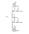
例えば、ポート数の増大に伴って、容量性負荷は増大し、それにより、整合回路網の変換係数および低Q整合構成要素の損失も同様に増大する。例えば、セルラハンドセット用途で切り替えられる帯域のうちのいくつかは、切り替えられる帯域の残りと比較してむしろ低いRF周波数であるため、SPnTスイッチをSP(n−m)T(単極(n−m)投)およびSPmT(単極m投)に分けることが可能である。但し、mは低周波数帯域ポートの数である。そのような回路構成の例を図2に示し、均等回路400を図4に示す(1つの広帯域ポートがアクティブであり、第1の切り替えユニット110の1つのポートがアクティブである)。C1(図4の第1の切り替えユニットのオフ状態寄生静電容量)の効果が低周波で小さいため、低帯域ポート(第2の切り替えユニット120のポート212c、d)は、直列になった並列インダクタLesdおよびLserにより整合され、その一方で、広帯域ノード(第1の切り替えユニット110のポート212a、b)は、Lesd、Lser、および低帯域トランジスタの寄生容量C2(第2の切り替えユニットのオフ状態寄生静電容量)により整合される。アンテナの低帯域ポート間に直接接続(第2の切り替えユニットから共通ポートへの接続)を提供すること、広帯域ポートの数を低減すること(例えば、従来のスイッチと比較して)、および/または整合キャパシタ(例えば、共通ポートにおけるシャント静電容量として通常配置される集中キャパシタ)を低帯域ポート切り替え要素の寄生容量(第2の切り替えユニットのオフ状態寄生静電容量)で置換することにより、部品表を低減すると共に、動作周波数範囲全体内のSPnTスイッチの挿入損失を改良することができる。
For example, as the number of ports increases, the capacitive load increases, thereby increasing the conversion factor of the matching network and the loss of low Q matching components as well. For example, since some of the bands switched in cellular handset applications are rather low RF frequencies compared to the rest of the switched band , SPnT switches can be SP (n−m) T (single pole (n−m ) Throw) and SPmT (single pole m throw). Here, m is the number of low frequency band ports. An example of such a circuit configuration is shown in FIG. 2 and an
この例では、整合ユニット130または整合回路網は、第1の切り替えユニット110に結合される側にシャントインダクタLesd、第1の切り替えユニット110と共通ポート102との間に直列インダクタLser、および共通ポート102に結合される側にシャントキャパシタとして第2の切り替えユニット120のオフ状態寄生静電容量を備える第1の切り替えユニット110と共通ポート102との間のπ要素が有効であるように設計され得、そして、直列インダクタLserの直列接続、シャントインダクタLesdの並列接続、および第1の切り替えユニット110のオフ状態寄生静電容量で構成されるシャントインピーダンスが、有効であるように設計され得る。
In this example, the
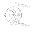
さらに、図5は、図4に示される概略図でシミュレートされた100MHz〜5GHzの周波数範囲での本発明によるスイッチの整合を示すスミス図500を示す。2つの周波数のうちの一方または両方の周波数のインピーダンス整合を既知のスイッチと比較して改良することができる。 In addition, FIG. 5 shows a Smith diagram 500 illustrating the matching of a switch according to the present invention in the frequency range of 100 MHz to 5 GHz simulated in the schematic shown in FIG. Impedance matching at one or both of the two frequencies can be improved compared to known switches.
以下に、図2に示される実施形態のいくつかの変形を説明する。 In the following, some variations of the embodiment shown in FIG. 2 will be described.
いくつかの実施形態は、第1の切り替えユニット110、第2の切り替えユニット120、および整合ユニット130を備える単極多投スイッチに関する。第2の切り替えユニット120は、共通ポート102に結合され、オフ状態寄生静電容量を備える。整合ユニット130は、第1の切り替えユニット110と共通ポート102との間に直接結合される。さらに、整合ユニット130は、第1の切り替えユニット110がアクティブであり、第2の切り替えユニット120が非アクティブである場合、第2の切り替えユニット120のオフ状態寄生静電容量と併せて、インピーダンス整合に寄与するように構成される。第1の切り替えユニット110は、第1の切り替え装置および第2の切り替え装置を備え、第2の切り替えユニット120は、第1の切り替え装置および第2の切り替え装置を備える。さらに、整合ユニット130は、直列インダクタLserおよび並列インダクタLesdを備える。整合ユニットの直列インダクタLserは、第1の切り替えユニット110と共通ポート102との間に電気的に結合され、並列インダクタLesdは、第1の端子で基準電位供給に結合されると共に、第2の端子で、第1の切り替えユニット110と直列インダクタLserとの間のノードに電気的に結合される。
Some embodiments relate to a single pole multiple throw switch comprising a
第1の切り替えユニット110の第1の切り替え装置は、整合ユニット130の直列インダクタLserおよび並列インダクタLesdに結合される第1の端子214aと、第1の切り替えユニット110の第1のポート212a(入力および/または出力)に結合される第2の端子214bとを備える。さらに、第1の切り替えユニット110の第1の切り替え装置は、制御信号を受信する制御入力214cを備える。
The first switching device of the
第1の切り替えユニット110の第2の装置は、整合ユニット130と第1の切り替えユニット110の第1の切り替え装置との間のノードに結合される第1の端子214aと、第1の切り替えユニット110の第2のポート212bに結合される第2の端子214bとを備える。さらに、第1の切り替えユニット110の第2の切り替え装置は、制御信号を受信する制御入力214cを備える。
The second device of the
第2の切り替えユニット120の第1の切り替え装置は、共通ポート102に結合される第1の端子214aと、第2の切り替えユニット120の第1のポート212cに結合される第2の端子214bとを備える。さらに、第2の切り替えユニット120の第1の切り替え装置は、制御信号を受信する制御入力214cを備える。
The first switching device of the
第2の切り替えユニット120の第2の切り替え装置は、共通ポート102に結合される第1の端子214aと、第2の切り替えユニット120の第2のポート212dに結合される第2の端子214bとを備える。さらに、第2の切り替えユニット120の第2の切り替え装置は、制御信号を受信する制御入力214cを備える。
The second switching device of the
いくつかのさらなる実施形態は、第1の切り替えユニット110、第2の切り替えユニット120、および整合ユニット130を備える単極多投スイッチに関する。第2の切り替えユニット120は、共通ポート102に結合され、オフ状態寄生静電容量を備える。整合ユニット130は、第1の切り替えユニット110と共通ポート102との間に電気的に結合され、第1の切り替えユニット110がアクティブであり、第2の切り替えユニット120が非アクティブである場合、第2の切り替えユニット120のオフ状態寄生静電容量と併せて、インピーダンス整合に寄与する。さらに、整合ユニット130は、第1の切り替えユニット110が非アクティブであり、第2の切り替えユニット120がアクティブである場合、インピーダンス整合に寄与する。単極多投スイッチは、少なくとも1つの低周波信号および少なくとも1つの高周波信号を切り替えるように構成され、整合ユニット130は、第1の切り替えユニット110により切り替えられる場合の高周波信号に対して整合ユニット130によって行われるインピーダンス整合のほうが、第2の切り替えユニット120により切り替えられる場合の高周波信号に対するインピーダンス整合よりも良好なように構成される。
Some further embodiments relate to a single pole multiple throw switch comprising a
いくつかの実施形態は、複数の送信ユニットおよび上述した概念による単極多投スイッチを備えるマルチバンド送信器に関する。単極多投スイッチの第1の切り替えユニットに結合された複数の送信ユニットの各送信ユニットは、第2の切り替えユニットに結合された複数の送信ユニットのすべての送信ユニットにより提供される信号のすべての周波数よりも高い周波数を有する信号を提供する。 Some embodiments relate to a multiband transmitter comprising a plurality of transmission units and a single pole multiple throw switch according to the concepts described above. Each transmission unit of the plurality of transmission units coupled to the first switching unit of the single pole multi-throw switch has all of the signals provided by all transmission units of the plurality of transmission units coupled to the second switching unit. Providing a signal having a higher frequency than
同じように、複数の受信ユニットおよび説明された概念による単極多投スイッチを備えるマルチバンド受信器も実現し得る。この場合、単極多投スイッチの第1の切り替えユニットに結合された複数の受信ユニットの各受信ユニットは、第2の切り替えユニットに結合された複数の受信ユニットのすべての受信ユニットにより受信される信号のすべての周波数よりも高い周波数を有する信号を受信するように構成される。 Similarly, a multi-band receiver comprising a plurality of receiving units and a single pole multi throw switch according to the described concept may be realized. In this case, each receiving unit of the plurality of receiving units coupled to the first switching unit of the single-pole multi-throw switch is received by all the receiving units of the plurality of receiving units coupled to the second switching unit. It is configured to receive a signal having a higher frequency than all the frequencies of the signal.
さらに、上述したマルチバンド送信器とマルチバンド受信器の概念を組み合わせることにより、マルチバンド送受信器を実現し得る。 Furthermore, a multiband transmitter / receiver can be realized by combining the concepts of the multiband transmitter and the multiband receiver described above.
上述した概念によりこのようにして、第1の切り替えユニット110を通る信号経路は、第2の切り替えユニットにより切り替えられる信号の周波数よりも高い周波数を有する信号に使用される。
The signal path through the
いくつかの実施形態は、単極多投RFスイッチに関する。 Some embodiments relate to a single pole multiple throw RF switch.
上述した概念に関連する用語RF(無線周波数)は、例えば、100MHz〜100GHzの周波数を含む。例えば、モバイル通信用途の周波数範囲全体が含まれる。しかし、より低い周波数(例えば、1MHz、またはそれよりも低い周波数から開始される)を無線周波数と考えてもよい。 The term RF (radio frequency) related to the concept described above includes, for example, frequencies from 100 MHz to 100 GHz. For example, the entire frequency range for mobile communication applications is included. However, lower frequencies (eg, starting from 1 MHz or lower) may be considered radio frequencies.
提案される回路は、単極多投RFスイッチの挿入損失を改良するのと同時に、アンテナポート整合回路網内の外部構成要素の数(既知のスイッチのスイッチ寄生容量を補償するために使用される)を低減することができる。 The proposed circuit is used to improve the insertion loss of single-pole multi-throw RF switches, while at the same time compensating the switch parasitic capacitance of the number of external components in the antenna port matching network ) Can be reduced.
提案されるRFスイッチは、2つの別個の切り替えブロック(切り替えユニット)を有し、例えば、1つは低周波で動作するチャネル専用であり、スイッチの共通ポートに直接接続され、ひいては整合キャパシタをスイッチの第2の広帯域部分の代わりにする。1つの並列インダクタおよび1つの直列インダクタからなる整合回路網(整合ユニット)から要求される低い変換係数が、有利であり、例えば、広帯域スイッチに必要なポート数が少なく、これはより低い全体挿入損失に繋がり、既知のスイッチにより使用される並列キャパシタをなくすことができる。 The proposed RF switch is has two separate switching blocks (switching units), for example, one is a channel dedicated to operate at a low frequency, the switch is connected directly to the common port of the switch, hence the matching capacitor to instead of the second wide-band part of. The low conversion factor required from a matching network consisting of one parallel inductor and one series inductor (matching unit) is advantageous, for example, fewer ports are required for a broadband switch, which results in lower overall insertion loss. The parallel capacitor used by the known switch can be eliminated.
単極多投スイッチを2つ以上のより小型のスイッチに分割し、部品数を低減したダイプレクサにより一緒に組み合わせる方法を提供し得、部品数の低減は、RFスイッチ自体の寄生容量を使用することにより達成し得る。高周波信号はスイッチの第1の部分(第1の切り替えユニット)により切り替えることができ、低周波信号はスイッチの第2の部分(第2の切り替えユニット)により切り替えることができるため、上述した単極多投スイッチはダイプレクサを表し得る。 A single-pole multi-throw switch can be divided into two or more smaller switches and combined together by a diplexer with a reduced number of parts, which can be reduced by using the parasitic capacitance of the RF switch itself Can be achieved. RF signals can be switched by a first part of the switch (first switching unit), unipolar low-frequency signal because it can be switched by the second part of the switch (second switching unit), the above-mentioned A multi-throw switch can represent a diplexer.
図6は、例示的な実施形態による単極多投スイッチを使用する方法600のフローチャートを示す。単極多投スイッチは、第1の切り替えユニット、第2の切り替えユニット、および整合ユニットを備える。第2の切り替えユニットは、共通ポートに結合され、オフ状態寄生静電容量を備える。整合ユニットは、第1の切り替えユニットと共通ポートとの間に電気的に結合され、第1の切り替えユニットがアクティブであり、第2の切り替えユニットが非アクティブの場合、第2の切り替えユニットの寄生オフ状態寄生容量と併せて、インピーダンス整合に寄与する。方法600は、共通ポートにおいて第1の周波数を有する信号を受信または提供するために第1の切り替えユニットをアクティブ化すること(610)および共通ポートにおいて第2の周波数を有する信号を受信または提供するために第2の切り替えユニットをアクティブ化すること(620)を含む。第1の周波数は第2の周波数よりも高い。
FIG. 6 shows a flowchart of a
いくつかの態様を装置の文脈で説明したが、これら態様が対応する方法の説明も表し、ブロックまたは装置が方法ステップまたは方法ステップの特徴に対応することが明らかである。同様に、方法ステップの文脈で説明された態様も、対応する装置の対応するブロック、アイテム、または特徴の説明を表す。 Although several aspects have been described in the context of an apparatus, it is clear that these aspects also represent a description of the corresponding method, and that a block or apparatus corresponds to a method step or method step feature. Similarly, aspects described in the context of method steps also represent descriptions of corresponding blocks, items, or features of corresponding devices.
請求項によっては、他の1つの請求項のみに関連するものもあるが、さらなる複数の請求項との組み合わせも可能であり得る。 Some claims may relate to only one other claim, but combinations with more than one claim may be possible.
100、200 単極多投スイッチ
102 共通ポート
110 第1の切り替えユニット
120 第2の切り替えユニット
130 整合ユニット
212a〜d ポート
214 切り替え装置
214a 第1の端子
214b 第2の端子
214c 制御入力
216a〜d 信号経路
400 均等回路
500 スミス図
100, 200 single-pole
Claims (14)
共通ポートに結合され、オフ状態寄生静電容量を備える第2の切り替えユニットと、
前記第1の切り替えユニットと前記共通ポートとの間に結合される整合ユニットであって、前記第1の切り替えユニットがアクティブであり、前記第2の切り替えユニットが非アクティブである場合、前記第2の切り替えユニットの前記オフ状態寄生静電容量と併せて、インピーダンス整合に寄与するように構成される、整合ユニットと
を備え、
前記第1の切り替えユニットおよび前記第2の切り替えユニットのそれぞれは切り替え装置を備え、各切り替え装置は、前記整合ユニットに結合される第1の端子と、前記共通ポートに提供する信号を受信すること、または前記共通ポートから受信される信号を提供することのうちの少なくとも一方を実行するように構成される第2の端子と、制御入力とを備え、
各切り替え装置は、前記制御入力において受信される制御信号によりアクティブ化されるように構成される、単極多投スイッチ。 A first switching unit;
A second switching unit coupled to the common port and comprising an off-state parasitic capacitance;
A matching unit coupled between the first switching unit and the common port, wherein the first switching unit is active and the second switching unit is inactive; together with the off-state parasitic capacitance of the switching unit, configured to contribute to impedance matching, and a matching unit,
Each of the first switching unit and the second switching unit includes a switching device, and each switching device receives a first terminal coupled to the matching unit and a signal provided to the common port. A second terminal configured to perform at least one of providing a signal received from the common port, and a control input,
Each switching device, Ru is configured to be activated by a control signal received at said control input, single pole multi throw switch.
共通ポートに結合され、オフ状態寄生静電容量を備える第2の切り替えユニットと、
前記第1の切り替えユニットと前記共通ポートとの間に結合される整合ユニットであって、前記第1の切り替えユニットがアクティブであり、前記第2の切り替えユニットが非アクティブである場合、前記第2の切り替えユニットの前記オフ状態寄生静電容量と併せて、インピーダンス整合に寄与するように構成される、整合ユニットと
を備え、
前記第1の切り替えユニットは、第1の切り替え装置および第2の切り替え装置を備え、前記第2の切り替えユニットは、第1の切り替え装置および第2の切り替え装置を備え、
前記整合ユニットは、直列インダクタおよび並列インダクタを備え、前記整合ユニットの前記直列インダクタは、前記第1の切り替え装置と前記共通ポートとの間に結合され、前記並列インダクタは、基準電位供給に結合された第1の端子と、前記第1の切り替えユニットと前記直列インダクタとの間のノードに結合される第2の端子とを備え、
前記第1の切り替えユニットの前記第1の切り替え装置は、前記整合ユニットの前記直列インダクタおよび前記並列インダクタに結合される第1の端子と、前記第1の切り替えユニットの第1のポートに結合される第2の端子とを備え、前記第1の切り替えユニットの前記第1の切り替え装置は、制御信号を受信するように構成される制御入力を備え、
前記第1の切り替えユニットの前記第2の切り替え装置は、前記整合ユニットと前記第1の切り替えユニットの前記第1の切り替え装置との間のノードに結合される第1の端子と、前記第1の切り替えユニットの第2のポートに結合される第2の端子とを備え、前記第1の切り替えユニットの前記第2の切り替え装置は、制御信号を受信するように構成される制御入力を備え、
前記第2の切り替えユニットの前記第1の切り替え装置は、前記共通ポートに直接結合される第1の端子と、前記第2の切り替えユニットの第1のポートに結合される第2の端子とを備え、前記第2の切り替えユニットの前記第1の切り替え装置は、制御信号を受信するように構成される制御入力を備え、
前記第2の切り替えユニットの前記第2の切り替え装置は、前記共通ポートに直接結合される第1の端子と、前記第2の切り替えユニットの第2のポートに結合される第2の端子とを備え、前記第2の切り替えユニットの前記第2の切り替え装置は、制御信号を受信するように構成される制御入力を備える、単極多投スイッチ。 A first switching unit;
A second switching unit coupled to the common port and comprising an off-state parasitic capacitance;
A matching unit coupled between the first switching unit and the common port, wherein the first switching unit is active and the second switching unit is inactive; A matching unit configured to contribute to impedance matching in conjunction with the off-state parasitic capacitance of the switching unit of
The first switching unit includes a first switching device and a second switching device, and the second switching unit includes a first switching device and a second switching device,
The matching unit comprises a series inductor and a parallel inductor, wherein the series inductor of the matching unit is coupled between said first switching device and the common port, wherein the parallel inductor is coupled to the reference potential supply A first terminal and a second terminal coupled to a node between the first switching unit and the series inductor;
The first switching device of the first switching unit is coupled to a first terminal coupled to the series inductor and the parallel inductor of the matching unit, and to a first port of the first switching unit. The first switching device of the first switching unit comprises a control input configured to receive a control signal;
The second switching device of the first switching unit includes a first terminal coupled to a node between the matching unit and the first switching device of the first switching unit, and the first And a second terminal coupled to a second port of the switching unit, wherein the second switching device of the first switching unit comprises a control input configured to receive a control signal,
Wherein said second switching unit first switching device has a first terminal coupled directly to the common port, and a second terminal coupled to a first port of the second switching unit The first switching device of the second switching unit comprises a control input configured to receive a control signal;
The second switching device of the second switching unit includes a first terminal directly coupled to the common port, and a second terminal coupled to the second port of the second switching unit. And the second switching device of the second switching unit comprises a control input configured to receive a control signal.
共通ポートに結合され、オフ状態寄生静電容量を備える第2の切り替えユニットと、
前記第1の切り替えユニットと前記共通ポートとの間に結合される整合ユニットであって、前記第1の切り替えユニットがアクティブであり、前記第2の切り替えユニットが非アクティブである場合、前記第1の切り替えユニットと前記共通ポートとの間のπ整合回路網として、前記第2の切り替えユニットの前記オフ状態寄生静電容量と併せて、インピーダンス整合に寄与するように構成される、整合ユニットと
を備え、
前記整合ユニットは、前記第1の切り替えユニットが非アクティブであり、前記第2の切り替えユニットがアクティブである場合、前記共通ポートと基準電位供給との間のシャント整合回路網として、インピーダンス整合に寄与するように構成され、
前記単極多投スイッチは、少なくとも1つの低周波信号および少なくとも1つの高周波信号を切り替えるように構成され、前記整合ユニットは、前記第1の切り替えユニットにより切り替えられる場合の高周波信号に対して前記整合ユニットにより行われるインピーダンス整合のほうが、前記第2の切り替えユニットにより切り替えられる場合の高周波信号に対して前記整合ユニットにより行われるインピーダンス整合よりも良好なように構成され、
前記第1の切り替えユニットおよび前記第2の切り替えユニットのそれぞれは切り替え装置を備え、各切り替え装置は、前記整合ユニットに結合される第1の端子と、前記共通ポートに提供する信号を受信すること、または前記共通ポートから受信される信号を提供することのうちの少なくとも一方を実行するように構成される第2の端子と、制御入力とを備え、
各切り替え装置は、前記制御入力において受信される制御信号によりアクティブ化されるように構成される、単極多投スイッチ。 A first switching unit;
A second switching unit coupled to the common port and comprising an off-state parasitic capacitance;
A matching unit coupled between the first switching unit and the common port, wherein the first switching unit is active and the second switching unit is inactive; A matching unit configured to contribute to impedance matching, together with the off-state parasitic capacitance of the second switching unit, as a π matching network between the switching unit and the common port Prepared,
The matching unit contributes to impedance matching as a shunt matching network between the common port and a reference potential supply when the first switching unit is inactive and the second switching unit is active. Configured to
The single-pole multi-throw switch is configured to switch between at least one low-frequency signal and at least one high-frequency signal, and the matching unit is configured to match the high-frequency signal when switched by the first switching unit. The impedance matching performed by the unit is configured to be better than the impedance matching performed by the matching unit for high-frequency signals when switched by the second switching unit ,
Each of the first switching unit and the second switching unit includes a switching device, and each switching device receives a first terminal coupled to the matching unit and a signal provided to the common port. A second terminal configured to perform at least one of providing a signal received from the common port, and a control input,
Each switching device, Ru is configured to be activated by a control signal received at said control input, single pole multi throw switch.
単極多投スイッチと
を備える、マルチバンド送信器であって、前記単極多投スイッチは、
第1の切り替えユニットと、
共通ポートに結合され、オフ状態寄生静電容量を備える第2の切り替えユニットと、
前記第1の切り替えユニットと前記共通ポートとの間に結合される整合ユニットであって、前記第1の切り替えユニットがアクティブであり、前記第2の切り替えユニットが非アクティブである場合、前記第2の切り替えユニットの前記オフ状態寄生静電容量と併せて、インピーダンス整合に寄与するように構成される、整合ユニットと
を備え、
前記第1の切り替えユニットに結合される前記複数の送信ユニットの各送信ユニットは、前記第2の切り替えユニットに結合された前記複数の送信ユニットのすべての送信ユニットにより提供される信号のすべての周波数よりも高い周波数の信号を提供するように構成され、
前記第1の切り替えユニットおよび前記第2の切り替えユニットのそれぞれは切り替え装置を備え、各切り替え装置は、前記整合ユニットに結合される第1の端子と、前記共通ポートに提供する信号を受信すること、または前記共通ポートから受信される信号を提供することのうちの少なくとも一方を実行するように構成される第2の端子と、制御入力とを備え、
各切り替え装置は、前記制御入力において受信される制御信号によりアクティブ化されるように構成される、マルチバンド送信器。 Multiple transmission units;
A multi-band transmitter comprising a single-pole multi-throw switch, wherein the single-pole multi-throw switch comprises:
A first switching unit;
A second switching unit coupled to the common port and comprising an off-state parasitic capacitance;
A matching unit coupled between the first switching unit and the common port, wherein the first switching unit is active and the second switching unit is inactive; A matching unit configured to contribute to impedance matching in conjunction with the off-state parasitic capacitance of the switching unit of
Each transmission unit of the plurality of transmission units coupled to the first switching unit has all frequencies of signals provided by all transmission units of the plurality of transmission units coupled to the second switching unit. Configured to provide a higher frequency signal ,
Each of the first switching unit and the second switching unit includes a switching device, and each switching device receives a first terminal coupled to the matching unit and a signal provided to the common port. A second terminal configured to perform at least one of providing a signal received from the common port, and a control input,
Each switching device, Ru is configured to be activated by a control signal received at said control input, a multi-band transmitter.
単極多投スイッチと
を備える、マルチバンド受信器であって、前記単極多投スイッチは、
第1の切り替えユニットと、
共通ポートに結合され、オフ状態寄生静電容量を備える第2の切り替えユニットと、
前記第1の切り替えユニットと前記共通ポートとの間に結合される整合ユニットであって、前記第1の切り替えユニットがアクティブであり、前記第2の切り替えユニットが非アクティブである場合、前記第2の切り替えユニットの前記オフ状態寄生静電容量と併せて、インピーダンス整合に寄与するように構成される、整合ユニットと
を備え、
前記第1の切り替えユニットに結合される前記複数の受信ユニットの各受信ユニットは、前記第2の切り替えユニットに結合された前記複数の受信ユニットのすべての受信ユニットにより受信される信号のすべての周波数よりも高い周波数の信号を受信するように構成され、
前記第1の切り替えユニットおよび前記第2の切り替えユニットのそれぞれは切り替え装置を備え、各切り替え装置は、前記整合ユニットに結合される第1の端子と、前記共通ポートに提供する信号を受信すること、または前記共通ポートから受信される信号を提供することのうちの少なくとも一方を実行するように構成される第2の端子と、制御入力とを備え、
各切り替え装置は、前記制御入力において受信される制御信号によりアクティブ化されるように構成される、マルチバンド受信器。 Multiple receiving units;
A multi-band receiver comprising a single-pole multi-throw switch, wherein the single-pole multi-throw switch is
A first switching unit;
A second switching unit coupled to the common port and comprising an off-state parasitic capacitance;
A matching unit coupled between the first switching unit and the common port, wherein the first switching unit is active and the second switching unit is inactive; A matching unit configured to contribute to impedance matching in conjunction with the off-state parasitic capacitance of the switching unit of
Each receiving unit of the plurality of receiving units coupled to the first switching unit has all frequencies of signals received by all receiving units of the plurality of receiving units coupled to the second switching unit. Configured to receive higher frequency signals ,
Each of the first switching unit and the second switching unit includes a switching device, and each switching device receives a first terminal coupled to the matching unit and a signal provided to the common port. A second terminal configured to perform at least one of providing a signal received from the common port, and a control input,
Each switching device, Ru is configured to be activated by a control signal received at said control input, a multi-band receiver.
第1の周波数を有する信号を前記共通ポートにおいて受信または提供するために前記第1の切り替えユニットをアクティブ化すること、および
第2の周波数を有する信号を前記共通ポートにおいて受信または提供するために前記第2の切り替えユニットをアクティブ化すること
を含み、前記第1の周波数は前記第2の周波数よりも高い、方法。 A method of using a single-pole multi-throw switch, wherein the single-pole multi-throw switch includes a first switching unit, a second switching unit, and a matching unit, and the second switching unit is coupled to a common port An off-state parasitic capacitance, wherein the matching unit is coupled between the first switching unit and the common port, each of the first switching unit and the second switching unit switching Each switching device includes: a first terminal coupled to the matching unit; receiving a signal provided to the common port; or providing a signal received from the common port. A second terminal configured to perform at least one and a control input, wherein each switching device is received at the control input. Is configured to be activated by that control signal, the first switching unit is is active, if the second switching unit is inactive, the off-state parasitic electrostatic the second switching unit In combination with capacitance, configured to contribute to impedance matching, the method includes:
Activating the first switching unit to receive or provide a signal having a first frequency at the common port, and to receive or provide a signal having a second frequency at the common port Activating a second switching unit, wherein the first frequency is higher than the second frequency.
共通ポートに結合され、オフ状態寄生静電容量を備える第2の切り替え手段と、
前記第1の切り替えユニットと前記共通ポートとの間に結合され、前記第1の切り替えユニットがアクティブであり、前記第2の切り替えユニットが非アクティブである場合、前記第2の切り替えユニットの前記オフ状態寄生静電容量と併せて、インピーダンス整合に寄与する、整合手段と
を備え、
前記第1の切り替え手段および前記第2の切り替え手段のそれぞれは切り替え装置を備え、各切り替え装置は、前記整合手段に結合される第1の端子と、前記共通ポートに提供する信号を受信すること、または前記共通ポートから受信される信号を提供することのうちの少なくとも一方を実行するように構成される第2の端子と、制御入力とを備え、
各切り替え装置は、前記制御入力において受信される制御信号によりアクティブ化されるように構成される、単極多投スイッチ。 First switching means;
A second switching means coupled to the common port and comprising an off-state parasitic capacitance;
Coupled between the first switching unit and the common port, the first switching unit being active and the second switching unit being inactive, the off of the second switching unit; Along with the state parasitic capacitance, the matching means contributes to impedance matching ,
Each of the first switching unit and the second switching unit includes a switching device, and each switching device receives a first terminal coupled to the matching unit and a signal provided to the common port. A second terminal configured to perform at least one of providing a signal received from the common port, and a control input,
Each switching device, Ru is configured to be activated by a control signal received at said control input, single pole multi throw switch.
Applications Claiming Priority (2)
| Application Number | Priority Date | Filing Date | Title |
|---|---|---|---|
| US12/609,199 | 2009-10-30 | ||
| US12/609,199 US8306481B2 (en) | 2009-10-30 | 2009-10-30 | Single pole multi throw switch |
Publications (2)
| Publication Number | Publication Date |
|---|---|
| JP2011097590A JP2011097590A (en) | 2011-05-12 |
| JP5259678B2 true JP5259678B2 (en) | 2013-08-07 |
Family
ID=43587244
Family Applications (1)
| Application Number | Title | Priority Date | Filing Date |
|---|---|---|---|
| JP2010244873A Active JP5259678B2 (en) | 2009-10-30 | 2010-11-01 | Single pole multi throw switch |
Country Status (4)
| Country | Link |
|---|---|
| US (1) | US8306481B2 (en) |
| EP (1) | EP2320514A1 (en) |
| JP (1) | JP5259678B2 (en) |
| CN (1) | CN102185594B (en) |
Families Citing this family (29)
| Publication number | Priority date | Publication date | Assignee | Title |
|---|---|---|---|---|
| US8421438B2 (en) | 2010-06-07 | 2013-04-16 | Skyworks Solutions, Inc. | Apparatus and method for diffusion sensing |
| US8249524B2 (en) * | 2010-09-10 | 2012-08-21 | Texas Instruments Incorporated | Transmit and receive performance of a near field communication device that uses a single antenna |
| US9100060B2 (en) | 2011-12-14 | 2015-08-04 | Infineon Technologies Ag | System and method for a radio frequency switch |
| WO2013106484A1 (en) * | 2012-01-09 | 2013-07-18 | Skyworks Solutions, Inc. | Devices and methods related to electrostatic discharge-protected cmos switches |
| US9588171B2 (en) | 2012-05-16 | 2017-03-07 | Infineon Technologies Ag | System and method for testing an integrated circuit |
| CN102970066B (en) * | 2012-09-17 | 2016-06-08 | 西安天和防务技术股份有限公司 | A kind of based on the transmodulator of microwave concentration of transmissions with dispersion transmission |
| JP6166608B2 (en) * | 2013-07-18 | 2017-07-19 | 太陽誘電株式会社 | Switch device and module |
| EP2871775B1 (en) * | 2013-11-12 | 2019-01-09 | Skyworks Solutions, Inc. | Devices and methods related to radio-frequency switches having improved performance |
| US11901243B2 (en) | 2013-11-12 | 2024-02-13 | Skyworks Solutions, Inc. | Methods related to radio-frequency switching devices having improved voltage handling capability |
| US9401706B2 (en) | 2014-01-27 | 2016-07-26 | Lattice Semiconductor Corporation | Apparatus, system and method for providing switching with a T-coil circuit |
| CN103928769B (en) * | 2014-03-25 | 2016-03-30 | 联想(北京)有限公司 | Aerial matching method, circuit and electronic equipment |
| US9641201B2 (en) | 2014-04-29 | 2017-05-02 | Infineon Technologies Ag | System and method for a radio frequency integrated circuit |
| US9847804B2 (en) * | 2014-04-30 | 2017-12-19 | Skyworks Solutions, Inc. | Bypass path loss reduction |
| US9515645B2 (en) * | 2014-06-03 | 2016-12-06 | Infineon Technologies Ag | System and method for a radio frequency switch |
| CN105429605B (en) | 2014-09-16 | 2019-03-08 | 天工方案公司 | The multiband equipment loaded with reduced frequency band |
| US9712197B2 (en) | 2015-08-28 | 2017-07-18 | Skyworks Solutions, Inc. | Tunable notch filter and contour tuning circuit |
| US9712196B2 (en) | 2015-08-28 | 2017-07-18 | Skyworks Solutions, Inc. | Tunable notch filter |
| US9966982B2 (en) | 2015-09-02 | 2018-05-08 | Skyworks Solutions, Inc. | Contour tuning circuit |
| CN105119591A (en) * | 2015-09-11 | 2015-12-02 | 天津大学 | CMOS (Complementary Metal Oxide Semiconductor) single-pole multi-throw switch for array detector |
| US9991889B2 (en) | 2016-02-09 | 2018-06-05 | Psemi Corporation | High throw-count RF switch |
| JP2017152896A (en) * | 2016-02-24 | 2017-08-31 | ソニー株式会社 | Semiconductor device, antenna switch circuit, module device, and wireless communication device |
| CN109412565B (en) * | 2017-08-18 | 2022-07-15 | 深圳指芯智能科技有限公司 | Multi-channel signal selection control circuit |
| US10491182B2 (en) * | 2017-10-12 | 2019-11-26 | Ethertronics, Inc. | RF signal aggregator and antenna system implementing the same |
| CN108365839A (en) * | 2018-04-28 | 2018-08-03 | 广东电网有限责任公司 | A Single Pole Multiple Throw Switch with Ring Structure |
| EP3588559B1 (en) * | 2018-06-29 | 2021-10-20 | Intel Corporation | Circuit for electrostatic discharge protection for wide frequency range multi-band interfaces |
| CN112468132A (en) * | 2020-10-30 | 2021-03-09 | 西安科锐盛创新科技有限公司 | Multi-coil coupling type single-pole four-throw switch and radio frequency integrated circuit |
| CN114826230B (en) * | 2022-04-28 | 2023-04-25 | 电子科技大学 | Ultra-wideband single-pole multi-throw radio frequency switch applying reconfigurable filter network |
| US20240154406A1 (en) * | 2022-11-08 | 2024-05-09 | Qualcomm Incorporated | Symmetric radio frequency (rf) electrostatic discharge (esd) dissipation switch |
| US20250105861A1 (en) * | 2023-09-22 | 2025-03-27 | Northrop Grumman Systems Corporation | Super-lattice castellated field effect transistor (slcfet) switch system |
Family Cites Families (25)
| Publication number | Priority date | Publication date | Assignee | Title |
|---|---|---|---|---|
| US5652599A (en) * | 1995-09-11 | 1997-07-29 | Qualcomm Incorporated | Dual-band antenna system |
| JP4351343B2 (en) * | 1999-12-24 | 2009-10-28 | 京セラ株式会社 | High frequency circuit |
| JP3736356B2 (en) | 2001-02-01 | 2006-01-18 | 日本電気株式会社 | High frequency switch circuit |
| US7057472B2 (en) | 2001-08-10 | 2006-06-06 | Hitachi Metals, Ltd. | Bypass filter, multi-band antenna switch circuit, and layered module composite part and communication device using them |
| JP4210978B2 (en) * | 2001-08-10 | 2009-01-21 | 日立金属株式会社 | Multiband antenna switch circuit, multiband antenna switch laminated module composite component, and communication device using the same |
| US6985712B2 (en) | 2001-08-27 | 2006-01-10 | Matsushita Electric Industrial Co., Ltd. | RF device and communication apparatus using the same |
| JP2003158467A (en) * | 2001-08-27 | 2003-05-30 | Matsushita Electric Ind Co Ltd | RF device and communication device using the same |
| JP2003078441A (en) | 2001-09-03 | 2003-03-14 | Matsushita Electric Ind Co Ltd | High frequency circuit device and mobile communication device |
| US6804502B2 (en) | 2001-10-10 | 2004-10-12 | Peregrine Semiconductor Corporation | Switch circuit and method of switching radio frequency signals |
| JP4009553B2 (en) | 2002-05-17 | 2007-11-14 | 日本電気株式会社 | High frequency switch circuit |
| JP3807615B2 (en) | 2002-12-05 | 2006-08-09 | 日立金属株式会社 | Multiband antenna switch circuit |
| JP3810011B2 (en) | 2003-08-08 | 2006-08-16 | Tdk株式会社 | High frequency switch module and multilayer substrate for high frequency switch module |
| US7236044B2 (en) * | 2003-10-14 | 2007-06-26 | The Board Of Trustees Of The Leland Stanford Junior University | Apparatus and method for adjusting the substrate impedance of a MOS transistor |
| JP2005123910A (en) * | 2003-10-16 | 2005-05-12 | Kyocera Corp | Composite demultiplexing circuit, chip part using the same, high frequency module, and wireless communication device |
| CN100530958C (en) * | 2003-10-16 | 2009-08-19 | 京瓷株式会社 | Composite channel splitting circuit, chip element using same, high-frequency model and wireless communication apparatus |
| JP2005191649A (en) | 2003-12-24 | 2005-07-14 | Toyota Central Res & Dev Lab Inc | High frequency switching circuit with filter function |
| US7391282B2 (en) | 2004-11-17 | 2008-06-24 | Matsushita Electric Industrial Co., Ltd. | Radio-frequency switch circuit and semiconductor device |
| US20060193730A1 (en) | 2005-02-25 | 2006-08-31 | Jacob Rosenstein | Method and apparatus for controlling microfluidic flow |
| US7504677B2 (en) | 2005-03-28 | 2009-03-17 | Freescale Semiconductor, Inc. | Multi-gate enhancement mode RF switch and bias arrangement |
| JP2006332778A (en) | 2005-05-23 | 2006-12-07 | Matsushita Electric Ind Co Ltd | High frequency switch circuit and semiconductor device using the same |
| JP4642570B2 (en) * | 2005-07-06 | 2011-03-02 | 日本電信電話株式会社 | High frequency switch circuit, wireless device and signal path switcher |
| US7910993B2 (en) | 2005-07-11 | 2011-03-22 | Peregrine Semiconductor Corporation | Method and apparatus for use in improving linearity of MOSFET's using an accumulated charge sink |
| JP2007110469A (en) | 2005-10-14 | 2007-04-26 | Matsushita Electric Ind Co Ltd | High frequency switch device |
| JP2008011503A (en) | 2006-05-31 | 2008-01-17 | Matsushita Electric Ind Co Ltd | High frequency switch circuit, high frequency switch device, and transmission module device |
| US7960772B2 (en) | 2007-04-26 | 2011-06-14 | Peregrine Semiconductor Corporation | Tuning capacitance to enhance FET stack voltage withstand |
-
2009
- 2009-10-30 US US12/609,199 patent/US8306481B2/en active Active
-
2010
- 2010-10-26 EP EP10188897A patent/EP2320514A1/en not_active Withdrawn
- 2010-10-29 CN CN2010106249594A patent/CN102185594B/en active Active
- 2010-11-01 JP JP2010244873A patent/JP5259678B2/en active Active
Also Published As
| Publication number | Publication date |
|---|---|
| US20110105055A1 (en) | 2011-05-05 |
| CN102185594A (en) | 2011-09-14 |
| EP2320514A1 (en) | 2011-05-11 |
| US8306481B2 (en) | 2012-11-06 |
| JP2011097590A (en) | 2011-05-12 |
| CN102185594B (en) | 2013-11-20 |
Similar Documents
| Publication | Publication Date | Title |
|---|---|---|
| JP5259678B2 (en) | Single pole multi throw switch | |
| US7808342B2 (en) | Harmonic phase tuning filter for RF switches | |
| CN105049012B (en) | For the system and method for RF IC | |
| US9166640B2 (en) | Adjustable impedance matching network | |
| EP0893882B1 (en) | High frequency switch device, front end unit and transceiver | |
| US7839234B2 (en) | Switching module with harmonic phase tuning filter | |
| KR101301209B1 (en) | CMOS switch for use in radio frequency switching and isolation enhancement method | |
| US20250070810A1 (en) | Configurable wideband split lna | |
| JP2005136948A (en) | Antenna switch circuit | |
| JP2007129571A (en) | High frequency switch circuit and semiconductor device | |
| CN105049016B (en) | The single-pole double throw RF switch and hilted broadsword of single-pole single-throw(SPST RF switch and its composition throw RF switch more | |
| JP2018050129A (en) | Receiving circuit, radio communication module, and radio communication apparatus | |
| US12425058B2 (en) | Radio frequency circuit and communication device | |
| US10951252B2 (en) | 5G NR configurable wideband RF front-end LNA | |
| US10511344B1 (en) | Transceiver resonant receive switch | |
| TWI790053B (en) | Radio frequency switch | |
| US20080238570A1 (en) | Spst Switch, Spdt Switch and Mpmt Switch | |
| WO2016125424A1 (en) | Power source supply circuit, amplifier, communication device, base station, and power source supply method | |
| CN108233912B (en) | Double-pole double-throw radio frequency switch | |
| US20230198565A1 (en) | Radio frequency switch | |
| CN103095269A (en) | Switch | |
| CN114785332B (en) | Three-frequency band single-pole multi-throw radio frequency switch based on reconfigurable filter network | |
| JP6373543B2 (en) | High frequency switch | |
| US20240030944A1 (en) | Configurable radio frequency (rf) multiplexing switch for rf front end in 4g/5g applications | |
| US20140062831A1 (en) | Switching circuit |
Legal Events
| Date | Code | Title | Description |
|---|---|---|---|
| A977 | Report on retrieval |
Free format text: JAPANESE INTERMEDIATE CODE: A971007 Effective date: 20120711 |
|
| A131 | Notification of reasons for refusal |
Free format text: JAPANESE INTERMEDIATE CODE: A131 Effective date: 20120724 |
|
| A601 | Written request for extension of time |
Free format text: JAPANESE INTERMEDIATE CODE: A601 Effective date: 20121022 |
|
| A601 | Written request for extension of time |
Free format text: JAPANESE INTERMEDIATE CODE: A601 Effective date: 20121023 |
|
| A602 | Written permission of extension of time |
Free format text: JAPANESE INTERMEDIATE CODE: A602 Effective date: 20121025 |
|
| A602 | Written permission of extension of time |
Free format text: JAPANESE INTERMEDIATE CODE: A602 Effective date: 20121026 |
|
| A521 | Request for written amendment filed |
Free format text: JAPANESE INTERMEDIATE CODE: A523 Effective date: 20130122 |
|
| TRDD | Decision of grant or rejection written | ||
| A01 | Written decision to grant a patent or to grant a registration (utility model) |
Free format text: JAPANESE INTERMEDIATE CODE: A01 Effective date: 20130402 |
|
| A61 | First payment of annual fees (during grant procedure) |
Free format text: JAPANESE INTERMEDIATE CODE: A61 Effective date: 20130424 |
|
| FPAY | Renewal fee payment (event date is renewal date of database) |
Free format text: PAYMENT UNTIL: 20160502 Year of fee payment: 3 |
|
| R150 | Certificate of patent or registration of utility model |
Ref document number: 5259678 Country of ref document: JP Free format text: JAPANESE INTERMEDIATE CODE: R150 Free format text: JAPANESE INTERMEDIATE CODE: R150 |
|
| R250 | Receipt of annual fees |
Free format text: JAPANESE INTERMEDIATE CODE: R250 |
|
| R250 | Receipt of annual fees |
Free format text: JAPANESE INTERMEDIATE CODE: R250 |
|
| R250 | Receipt of annual fees |
Free format text: JAPANESE INTERMEDIATE CODE: R250 |
|
| R250 | Receipt of annual fees |
Free format text: JAPANESE INTERMEDIATE CODE: R250 |
|
| R250 | Receipt of annual fees |
Free format text: JAPANESE INTERMEDIATE CODE: R250 |
|
| R250 | Receipt of annual fees |
Free format text: JAPANESE INTERMEDIATE CODE: R250 |
|
| R250 | Receipt of annual fees |
Free format text: JAPANESE INTERMEDIATE CODE: R250 |
|
| R250 | Receipt of annual fees |
Free format text: JAPANESE INTERMEDIATE CODE: R250 |
|
| R250 | Receipt of annual fees |
Free format text: JAPANESE INTERMEDIATE CODE: R250 |
|
| R250 | Receipt of annual fees |
Free format text: JAPANESE INTERMEDIATE CODE: R250 |