JP5259666B2 - Nonvolatile semiconductor memory device - Google Patents
Nonvolatile semiconductor memory device Download PDFInfo
- Publication number
- JP5259666B2 JP5259666B2 JP2010212720A JP2010212720A JP5259666B2 JP 5259666 B2 JP5259666 B2 JP 5259666B2 JP 2010212720 A JP2010212720 A JP 2010212720A JP 2010212720 A JP2010212720 A JP 2010212720A JP 5259666 B2 JP5259666 B2 JP 5259666B2
- Authority
- JP
- Japan
- Prior art keywords
- memory cell
- voltage
- word line
- write
- nth
- Prior art date
- Legal status (The legal status is an assumption and is not a legal conclusion. Google has not performed a legal analysis and makes no representation as to the accuracy of the status listed.)
- Active
Links
Images


Classifications
-
- G—PHYSICS
- G11—INFORMATION STORAGE
- G11C—STATIC STORES
- G11C11/00—Digital stores characterised by the use of particular electric or magnetic storage elements; Storage elements therefor
- G11C11/56—Digital stores characterised by the use of particular electric or magnetic storage elements; Storage elements therefor using storage elements with more than two stable states represented by steps, e.g. of voltage, current, phase, frequency
- G11C11/5621—Digital stores characterised by the use of particular electric or magnetic storage elements; Storage elements therefor using storage elements with more than two stable states represented by steps, e.g. of voltage, current, phase, frequency using charge storage in a floating gate
- G11C11/5628—Programming or writing circuits; Data input circuits
-
- G—PHYSICS
- G11—INFORMATION STORAGE
- G11C—STATIC STORES
- G11C16/00—Erasable programmable read-only memories
- G11C16/02—Erasable programmable read-only memories electrically programmable
- G11C16/06—Auxiliary circuits, e.g. for writing into memory
-
- G—PHYSICS
- G11—INFORMATION STORAGE
- G11C—STATIC STORES
- G11C16/00—Erasable programmable read-only memories
- G11C16/02—Erasable programmable read-only memories electrically programmable
- G11C16/06—Auxiliary circuits, e.g. for writing into memory
- G11C16/10—Programming or data input circuits
-
- G—PHYSICS
- G11—INFORMATION STORAGE
- G11C—STATIC STORES
- G11C16/00—Erasable programmable read-only memories
- G11C16/02—Erasable programmable read-only memories electrically programmable
- G11C16/06—Auxiliary circuits, e.g. for writing into memory
- G11C16/34—Determination of programming status, e.g. threshold voltage, overprogramming or underprogramming, retention
- G11C16/3436—Arrangements for verifying correct programming or erasure
- G11C16/3454—Arrangements for verifying correct programming or for detecting overprogrammed cells
Landscapes
- Engineering & Computer Science (AREA)
- Computer Hardware Design (AREA)
- Read Only Memory (AREA)
- Semiconductor Memories (AREA)
- Non-Volatile Memory (AREA)
Description
実施形態は、積層型のメモリセル構造を有する不揮発性半導体記憶装置に関する。 Embodiments described herein relate generally to a nonvolatile semiconductor memory device having a stacked memory cell structure.
近年、NAND型フラッシュメモリのビット密度向上に向けたアプローチとして、メモリセルを積層した積層型NAND、いわゆるBiCS(Bit-Cost Scalable)タイプのメモリが提案されている。 In recent years, as an approach for improving the bit density of a NAND flash memory, a stacked NAND in which memory cells are stacked, a so-called BiCS (Bit-Cost Scalable) type memory has been proposed.
本実施形態は、データ書き込みの高速化をはかり得る不揮発性半導体記憶装置を提供する。 The present embodiment provides a nonvolatile semiconductor memory device capable of speeding up data writing.
実施形態の不揮発性半導体記憶装置によれば、半導体基板上に積層された複数のワード線に、電荷蓄積層を有する複数のメモリセルがそれぞれ接続され、且つ、隣接するメモリセル間で電荷蓄積層が連続しているセル構造のメモリセルアレイと、前記メモリセルアレイのn番目(nは自然数)のワード線に接続されたメモリセル群にデータを書き込む際に、(n−1)番目及び(n+1)番目のワード線に接続されたメモリセル群に同一の書き込み電圧を同時に印加するよう制御する制御回路と、を具備したことを特徴とする。 According to the nonvolatile semiconductor memory device of the embodiment, a plurality of memory cells having a charge storage layer are respectively connected to a plurality of word lines stacked on a semiconductor substrate, and the charge storage layer is disposed between adjacent memory cells. Are written in a memory cell array having a continuous cell structure and a memory cell group connected to the nth (n is a natural number) word line of the memory cell array, the (n−1) th and (n + 1) th And a control circuit for controlling the same write voltage to be simultaneously applied to the memory cell group connected to the th word line.
以下、実施の形態について、図面を参照して説明する。この説明に際し、全図にわたり、共通する部分には共通する参照符号を付す。また、図面の寸法比率は、図示の比率に限定されるものではない。 Hereinafter, embodiments will be described with reference to the drawings. In the description, common parts are denoted by common reference symbols throughout the drawings. Further, the dimensional ratios in the drawings are not limited to the illustrated ratios.
(第1の実施形態)
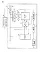
まず、第1の実施形態に係わる3次元積層型不揮発性半導体記憶装置を例として、図6のブロック図を用いて説明する。
(First embodiment)
First, the three-dimensional stacked nonvolatile semiconductor memory device according to the first embodiment will be described as an example with reference to the block diagram of FIG.
[不揮発性半導体記憶装置の構成]
本実施形態の3次元積層型不揮発性半導体記憶装置は、BiCSフラッシュメモリ10と、メモリコントローラ(外部コントローラともいう)20とを有する。ここで、BiCSフラッシュメモリ10は、メモリセルアレイ11、センスアンプ12、カラムアドレスバッファ/カラムデコーダ13、ロウデコーダ14、制御回路(内部コントローラともいう)15、電圧生成回路16、パワーオン検出回路17、ロウアドレスバッファ18、入出力バッファ19を備える。
[Configuration of Nonvolatile Semiconductor Memory Device]
The three-dimensional stacked nonvolatile semiconductor memory device according to this embodiment includes a BiCS
<メモリセルアレイ>
まず、本実施形態のメモリセルアレイ1について、図1乃至図3を用いて説明する。
<Memory cell array>
First, the
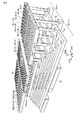
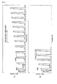
メモリセルアレイ1は、図1の鳥瞰図に示すような素子構造を有する。このメモリセルアレイ1は、消去の一単位となる複数のブロックを複数個、有する。説明の便宜上、図1では、2つのブロックBK<i>,BK<i+1> について図示した。
The
図1に示すように、このブロックは、ソース拡散層32、ソース拡散層32上方に形成された導電層(図1では、SGS,SGD,WL<0> 乃至WL<3> を示す)、活性層AAなどにより形成される。
As shown in FIG. 1, this block includes a
<<ソース拡散層>>
半導体基板31内に形成されるソース拡散層32は、例えば、同一プレーン内の全ブロックBKに共通に1つ設けられる。ソース拡散層32は、コンタクトプラグPSLを介して、ソース線SL・M1に接続される。
<< Source diffusion layer >>
For example, one
また、ソース拡散層32上には、例えば、導電性ポリシリコンから構成される3以上の導電層が層間絶縁膜(図示略)を介して積層される。
Further, on the
<<導電層>>
本実施形態では、導電層は、層間絶縁膜を介して6層積層された構造となっている。図1では、導電膜は、ワード線WL<0> 乃至WL<3> と、ドレイン側セレクトゲート線(第1セレクトゲート線)SGDと、ソース側セレクトゲート線(第2セレクトゲート線)SGSである。
<< Conductive layer >>
In the present embodiment, the conductive layer has a structure in which six layers are stacked via an interlayer insulating film. In FIG. 1, the conductive films are word lines WL <0> to WL <3>, a drain side select gate line (first select gate line) SGD, and a source side select gate line (second select gate line) SGS. is there.
最上層(図1における、SGD<0> 乃至SGD<5> )を除く残りの5つの導電層は、1つのブロックBK<i+1> 内でそれぞれプレート状に形成される。また、6つの導電層のx方向の端部は、各々の導電層にコンタクトをとるために全体として階段状に形成される。例えば、ワード線WL<0> は、ソース側セレクトゲート線SGS上方に形成されるが、ソース側セレクトゲート線SGSのコンタクトをとるための領域の上方には形成されない。すなわち、ワード線WL<0> は、ソース側セレクトゲート線SGSよりもx軸方向の幅が短く形成される。同様に、ワード線WL<1> は、ワード線WL<2> よりもx軸方向の幅が短く形成され、ワード線WL<2> は、ワード線WL<3> よりもx軸方向の幅が短く形成され、ワード線WL<3> は、ドレイン側セレクトゲート線SGDよりもx軸方向の幅が短く形成される。 The remaining five conductive layers excluding the uppermost layer (SGD <0> to SGD <5> in FIG. 1) are each formed in a plate shape within one block BK <i + 1>. The ends of the six conductive layers in the x direction are formed in a step shape as a whole in order to make contact with each conductive layer. For example, the word line WL <0> is formed above the source side select gate line SGS, but is not formed above the region for making contact with the source side select gate line SGS. That is, the word line WL <0> is formed to have a shorter width in the x-axis direction than the source side select gate line SGS. Similarly, the word line WL <1> is formed to have a shorter width in the x-axis direction than the word line WL <2>, and the word line WL <2> is wider in the x-axis direction than the word line WL <3>. And the word line WL <3> is formed to have a shorter width in the x-axis direction than the drain-side select gate line SGD.
最下層は、ソース側セレクトゲート線SGSとなり、最下層及び最上層を除く残りの4つの導電層は、ワード線WL<0>,WL<1>,WL<2>,WL<3> となる。 The lowermost layer is the source side select gate line SGS, and the remaining four conductive layers excluding the lowermost layer and the uppermost layer are the word lines WL <0>, WL <1>, WL <2>, WL <3>. .
最上層は、x方向に延びるライン状の複数の導電線から構成される。1つのブロックBK<i+1> 内には、例えば、6本の導電線が配置される。最上層の例えば6本の導電線は、ドレイン側セレクトゲート線SGD<0> 〜SGD<5> となる。 The uppermost layer is composed of a plurality of linear conductive lines extending in the x direction. For example, six conductive lines are arranged in one block BK <i + 1>. For example, six conductive lines in the uppermost layer become drain side select gate lines SGD <0> to SGD <5>.
<<活性層>>
そして、NANDストリング(図3で後述する)を構成するための複数の活性層(アクティブエリア)AAは、z方向(半導体基板の表面に対して垂直方向)に柱状に形成されており、ソース拡散層32から複数の導電層を突き抜けてビット線BLに達するように形成される。
<< Active layer >>
A plurality of active layers (active areas) AA for forming a NAND string (described later in FIG. 3) are formed in a column shape in the z direction (perpendicular to the surface of the semiconductor substrate), and source diffusion It is formed so as to penetrate the plurality of conductive layers from the
複数の活性層AAの上端は、y方向に延びる複数のビット線BL<0> 〜BL<m> に接続される。また、ソース側セレクトゲート線SGSは、コンタクトプラグPSGS を介して、x方向に延びる引き出し線SGS−M1に接続され、ワード線WL<0> 〜WL<3> は、それぞれ、コンタクトプラグPWL<0>〜PWL<3> を介して、x方向に延びる引き出し線WL<0>・M1〜WL<3>・M1に接続される。 The upper ends of the plurality of active layers AA are connected to a plurality of bit lines BL <0> to BL <m> extending in the y direction. The source side select gate line SGS is connected to the lead line SGS-M1 extending in the x direction via the contact plug P SGS , and the word lines WL <0> to WL <3> are respectively connected to the contact plug P WL. via <0> ~P WL <3> , it is connected to the lead line WL <0> · M1~WL <3 > · M1 extending in the x-direction.
さらに、ドレイン側セレクトゲート線SGD<0> 〜SGD<5> は、それぞれ、コンタクトプラグPSGD<0>〜PSGD<5> を介して、x方向に延びる引き出し線SGD<0>・M1〜SGD<5>・M1に接続される。 Further, the drain-side select gate lines SGD <0> to SGD <5> are drawn out through the contact plugs P SGD <0> to P SGD <5> in the x direction, respectively. Connected to SGD <5> · M1.
複数のビット線BL<0> 〜BL<m> 及び引き出し線SGS・M1,WL<0>・M1,WL<1>・M1〜WL<3>・M1,SGD<0>・M1〜SGD<5>・M1は、例えば、金属から構成される。 A plurality of bit lines BL <0> to BL <m> and lead lines SGS, M1, WL <0>, M1, WL <1>, M1 to WL <3>, M1, SGD <0>, M1 to SGD < 5> · M1 is made of metal, for example.
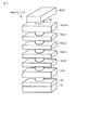
図2は、1つのNANDストリングの鳥瞰図を示している。図1に示すようなブロックBKには、図2に示すようなNANDストリングを複数個(例えば、24個)、有する。このNANDストリングは、複数のメモリセルと、ソース側選択ゲートトランジスタと、ドレイン側選択トランジスタとを有する。 FIG. 2 shows a bird's eye view of one NAND string. A block BK as shown in FIG. 1 has a plurality (for example, 24) of NAND strings as shown in FIG. This NAND string includes a plurality of memory cells, a source side select gate transistor, and a drain side select transistor.
図3は、1つのNANDストリングの構造例を示す断面図であり、(a)は全体構成を示し、(b)は一部を拡大して示している。 3A and 3B are cross-sectional views showing an example of the structure of one NAND string, where FIG. 3A shows the overall configuration, and FIG. 3B shows an enlarged part.
図2及び図3に示すように、メモリセルは、半導体基板31表面に対して垂直方向(z方向)に柱状に形成された活性層AAとワード線WL<0> 〜WL<3> との交差部分に形成される。また、ソース側選択ゲートトランジスタは、活性層AAとソース側セレクトゲート線SGSとの交差部分に形成され、ドレイン側選択ゲートトランジスタは、活性層AAとドレイン側セレクトゲート線SGDとの交差部分に形成される。 As shown in FIGS. 2 and 3, the memory cell includes an active layer AA formed in a columnar shape in a direction perpendicular to the surface of the semiconductor substrate 31 (z direction) and word lines WL <0> to WL <3>. Formed at the intersection. The source side select gate transistor is formed at the intersection between the active layer AA and the source side select gate line SGS, and the drain side select gate transistor is formed at the intersection between the active layer AA and the drain side select gate line SGD. Is done.
ソース側セレクトゲート線SGSとドレイン側セレクトゲート線SGDは、複数のワード線WL<0> 〜WL<3> を挟むように形成される。 The source side select gate line SGS and the drain side select gate line SGD are formed so as to sandwich a plurality of word lines WL <0> to WL <3>.
3次元構造のNANDストリングの特徴の一つは、ドレイン側セレクトゲート線SGD<5>が、柱状の活性層AAの側面を取り囲む構造を有している点にある。 One of the features of the three-dimensional NAND string is that the drain side select gate line SGD <5> has a structure surrounding the side surface of the columnar active layer AA.
このため、例えば、複数の活性層AAを細くして、半導体基板31上により多くの活性層AAを形成し、大容量化を図っても、NANDストリングを構成する選択トランジスタの駆動力を十分に確保できることになる。
For this reason, for example, even if a plurality of active layers AA are thinned to form a larger number of active layers AA on the
図3に示すように、1つのNANDストリングを構成している複数のメモリセルMC及び選択ゲートトランジスタST(ソース側選択ゲートトランジスタ、ドレイン側選択ゲートトランジスタ)は、層間絶縁膜37を介してz方向に積層される。
As shown in FIG. 3, a plurality of memory cells MC and select gate transistors ST (source side select gate transistors, drain side select gate transistors) constituting one NAND string are arranged in the z direction via an
メモリセルMCは、MONOS構造を有する。MONOS構造とは、電荷蓄積層がSiN等の窒化物などの絶縁体から構成されるメモリセル構造のことである。即ち、図3(b)に示すように、メモリセルMCは、電荷蓄積層34が、例えば、2つの絶縁膜33,35に挟み込まれた構造を有した、ONO(Oxide-Nitride-Oxide)の構成となっている。電荷蓄積層34と活性層AAとの間には、絶縁膜33が介在している。絶縁膜33は、データの書き込み時にはトンネル絶縁膜として機能し、データの保持時には電荷が活性層AAにリークするのを防止する。電荷蓄積層34と制御ゲート36との間には、ブロック絶縁膜35が介在している。ブロック絶縁膜35は、電荷蓄積層34に捕獲された電荷が制御ゲート36にリークするのを防止する。制御ゲート36は、ワード線WLに接続される。
Memory cell MC has a MONOS structure. The MONOS structure is a memory cell structure in which the charge storage layer is made of an insulator such as a nitride such as SiN. That is, as shown in FIG. 3B, the memory cell MC has an ONO (Oxide-Nitride-Oxide) structure in which the
なお、メモリセルMCは、ブロック絶縁膜35を設けないMNOS構造のメモリセルでもよい。
The memory cell MC may be a memory cell having an MNOS structure in which the
1つのワード線WLを共有する各NANDストリング内のメモリセルトランジスタMの集合は、データ読み出し及び書き込みの単位となるページを構成する。また、ワード線WLを共有する複数のNANDストリングの集合は、データ消去の単位となるブロックを構成する。 A set of memory cell transistors M in each NAND string sharing one word line WL constitutes a page that is a unit of data reading and writing. A set of a plurality of NAND strings sharing the word line WL constitutes a block serving as a data erasing unit.
<センスアンプ及びカラムアドレスバッファ/カラムデコーダ>
図6に示すように、センスアンプ12は、ビット線BLを介してメモリセルアレイ11と接続される。センスアンプ12は、読み出しの際にメモリセルアレイ11のデータをページ単位で読み出しを行い、書き込みの際にメモリセルアレイ11にデータをページ単位で書き込む。
<Sense amplifier and column address buffer / column decoder>
As shown in FIG. 6, the
また、センスアンプ12はカラムアドレスバッファ/カラムデコーダ13とも接続されており、センスアンプ12はカラムアドレスバッファ/カラムデコーダ13(後述する)から入力される選択信号をデコードして、ビット線BLのいずれかを選択し、駆動する。
The
センスアンプ12は、書き込む際のデータを保持するデータラッチの機能も兼ねる。本実施形態のセンスアンプでは、それぞれのセンスアンプには複数個(通常、2bit/cellのMLCでは3つ)のデータラッチ回路を有する。
The
カラムアドレスバッファ/カラムデコーダ13は、メモリコントローラ20からロウアドレスバッファ18を介して入力されるカラムアドレス信号を一時的に格納し、カラムアドレス信号に従ってビット線BLのいずれかを選択する選択信号をセンスアンプ12に出力する。
The column address buffer /
<ロウデコーダ>
ロウデコーダ14は、ロウアドレスバッファ18を介して入力されるロウアドレス信号をデコードして、ワード線WL及びセレクトゲート線SGD,SGSを選択し、駆動する。
<Row decoder>
The
なお、本実施形態のBiCSフラッシュメモリ10には、外部入出力端子I/O(図示略)が設けられており、この外部入出力端子I/Oを介して入出力バッファ19とメモリコントローラ20のデータの授受が行われる。外部入出力端子I/Oを介して入力されるアドレス信号は、ロウアドレスバッファ18を介してロウデコーダ14及びカラムアドレスバッファ/カラムデコーダ13に出力される。
Note that the
<制御回路>
制御回路15は、メモリコントローラ20を介して供給される各種外部制御信号(書き込みイネーブル信号WEn、読み出しイネーブル信号REn、コマンドラッチイネーブル信号CLE、アドレスラッチイネーブル信号ALE等)とコマンドCMDに基づいて、データ書き込み及び消去のシーケンス制御及び読み出しの動作・制御を行う。制御回路15は、パワーオン検出回路17から入力される検知信号を受けて、初期化動作を自動的に行う。
<Control circuit>
The
<電圧生成回路>
電圧発生回路16は、制御回路15により制御されて、書き込み、消去及び読み出しの動作に必要な各種内部電圧を発生するもので、電源電圧より高い内部電圧を発生するために昇圧回路が用いられる。
<Voltage generation circuit>
The
<パワーオン検出回路>
パワーオン検出回路17は、制御回路15に接続される。パワーオン検出回路17は、電源の投入を検出し、制御回路15に検知信号を出力する。
<Power-on detection circuit>
The power-on
<メモリコンロトーラ>
メモリコンロトーラ20は、BiCSフラッシュメモリ10に必要なコマンドなどを出力し、BiCSフラッシュメモリ10の動作モード(後述する、第1の書き込みモード、第2の書き込みモードを含む。)を設定し、読み出し及び書き込みを行う。
<Memory controller>
The memory controller 20 outputs a command or the like necessary for the
[本実施形態の経緯]
ここで、本実施形態の不揮発性半導体メモリは、図3(b)に示すように、隣接するメモリセル間で電荷蓄積層34がつながっている。このため、平面NANDタイプの不揮発性半導体メモリのようにメモリセルの消去レベルを負にしたVthバジェットを使用すると、本実施形態の不揮発性半導体メモリのデータリテンションが悪化する場合がある。その支配的要因はいわゆる電荷の横抜けである。これは、例えば同一チャネルのボディで正の閾値のメモリセルと負の閾値のメモリセルが隣接した場合に起こる。
[Background of this embodiment]
Here, in the nonvolatile semiconductor memory of this embodiment, as shown in FIG. 3B, the
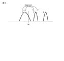
すなわち、閾値を正に書き込んだメモリセルに隣接するメモリセルが閾値が負の消去セルの場合、物理的につながった電荷蓄積層間でホールとエレクトロンの再結合が起こり、正の閾値に書き込んだメモリセルの閾値の低下と、負の閾値のメモリセルの閾値の上昇が起こる。これにより、データリテンション特性が低下する。以降、このようなデータリテンション特性の低下をデータの横抜けと呼び、データの横抜けが起こるデータパターンをデータの横抜けパターンと呼ぶ。そこで、このデータの横抜けを防ぐために、消去レベルを正にしておくことが有効である。 That is, when the memory cell adjacent to the memory cell in which the threshold is written positive is an erase cell having a negative threshold, recombination of holes and electrons occurs between physically connected charge storage layers, and the memory written in the positive threshold A cell threshold decrease and a negative threshold memory cell threshold increase occur. Thereby, the data retention characteristic is deteriorated. Hereinafter, such a decrease in data retention characteristics is referred to as data breakthrough, and a data pattern in which data breakthrough occurs is referred to as data breakthrough pattern. Therefore, it is effective to set the erasure level to be positive in order to prevent this data from passing through.
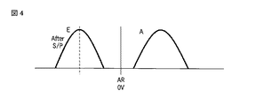
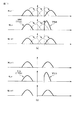
図4は、1bit/cellの平面NANDタイプの不揮発性半導体記憶装置のVthバジェットを示す図である。平面NANDタイプの不揮発性半導体記憶装置では、書き込みセルを正の閾値に書き込み、非書き込みセルについては、閾値が負の消去状態のままにしておく。この場合には、書き込む際に分布を一つ書き込むだけでよいため、書き込み電圧のステップアップ幅であるΔVPGM を大きく設定できる。その結果、書き込みループ回数が少なくなり、非常に高速の書き込みが実現できる。 FIG. 4 is a diagram showing a Vth budget of a 1-bit / cell planar NAND type nonvolatile semiconductor memory device. In a planar NAND type nonvolatile semiconductor memory device, a write cell is written to a positive threshold value, and a non-write cell is left in an erased state where the threshold value is negative. In this case, since only one distribution needs to be written at the time of writing, ΔV PGM that is the step-up width of the write voltage can be set large. As a result, the number of write loops is reduced, and extremely high-speed writing can be realized.
図5は、1bit/cellのBiCSタイプの先行の不揮発性半導体記憶装置のVthバジェットを示す図である。先に説明したデータの横抜けを防止するために、非書き込みセルについて、初期の消去状態(第1の消去状態ともいう)から閾値電圧が正である消去状態(第2の消去状態ともいい、図5におけるE’レベルを意味する)への書き込みが必要で、書き込みセルについては、更に高いAレベルへの書き込みを行う必要がある。なお、第1の消去状態は、全ての非書き込みセルの閾値電圧が負である状態に限られず、非書き込みセルの一部の閾値電圧が正の状態であってもよい。また、第2の消去状態は、全ての非書き込みセルの閾値分布が正の状態である。 FIG. 5 is a diagram showing the Vth budget of a prior nonvolatile semiconductor memory device of 1 bit / cell BiCS type. In order to prevent the data passing through described above, the non-written cell is erased from an initial erased state (also referred to as a first erased state) to a positive threshold voltage (also referred to as a second erased state). 5 (which means the E ′ level in FIG. 5) is required, and the write cell needs to be written to a higher A level. Note that the first erase state is not limited to a state in which the threshold voltages of all the non-written cells are negative, and a part of the threshold voltages of the non-written cells may be positive. The second erase state is a state in which the threshold distribution of all non-written cells is positive.
先行の不揮発性半導体記憶装置の場合には、正に2つの閾値分布を書く必要があることから、メモリセルへの書き込み過ぎを防止すべく初期VPGM を低くする必要があるとともに、E’レベルの上裾とAレベルの下裾とのマージンを確保すべくΔVPGM をアッパーページ書き込みと同程度に小さく設定し、閾値分布を細く書き込む必要がある。 In the case of the preceding nonvolatile semiconductor memory device, since it is necessary to write exactly two threshold distributions, it is necessary to lower the initial V PGM to prevent excessive writing to the memory cell, and at the E ′ level. In order to ensure a margin between the upper skirt and the lower skirt of the A level, ΔV PGM needs to be set as small as the upper page write and the threshold distribution needs to be written finely.
そのため、図5の場合と比較して、初期VPGM を低く、ΔVPGM が小さく、且つAレベルを高いレベルまで書き込む必要があり、書き込む際に印加するパルス数が増大する。その結果、書き込み時間が大幅に長くなる。 Therefore, compared with the case of FIG. 5, it is necessary to write the initial V PGM low, ΔV PGM small, and the A level to a high level, and the number of pulses applied at the time of writing increases. As a result, the writing time is significantly increased.
そこで、この問題を解決するために本実施形態では、消去レベルを正に書き戻す必要のない、高速なSLC書き込みを実現することで、データ書き込みの高速化を図りうる不揮発性半導体記憶装置を提供する。 Therefore, in order to solve this problem, the present embodiment provides a nonvolatile semiconductor memory device capable of speeding up data writing by realizing high-speed SLC writing without having to write back the erase level to the positive level. To do.
[不揮発性半導体記憶装置の動作]
次に、本実施形態の不揮発性半導体記憶装置の書き込み動作について、図7のフローチャート図を用いて説明する。
[Operation of Nonvolatile Semiconductor Memory Device]
Next, the write operation of the nonvolatile semiconductor memory device of this embodiment will be described using the flowchart of FIG.
ステップS1では、メモリコントローラ20から専用コマンドが発行され、専用コマンドが、入出力バッファ19を介して制御回路15に入力される。また、アドレス信号は、入出力バッファ19を介してロウアドレスバッファ18に入力される。さらに、書き込みデータは入出力バッファ19を介してセンスアンプ12のデータラッチ回路(図示略)に入力される。
In
ステップS2で、制御回路15は、ステップS1で入力されたコマンドを受けて、高速書き込み動作モード信号(第1の書き込みモード信号ともいう)を生成する。
In step S2, the
ステップS3で、制御回路15は、電圧を生成するためのタイミング制御信号、電圧設定信号を電圧生成回路16に出力する。
In step S <b> 3, the
ステップS4で、制御回路15は、アドレス制御信号、メモリセルへのアクセス制御信号に基づいて、センスアンプ12,ロウデコーダ14及び電圧生成回路16を制御し、選択されたブロックBK内の選択されたn番目のワード線WL(選択ワード線WLともいう)と、(n±1)番目のワード線WLに同一の書き込み電圧VPGM を印加する。ただし、nは自然数である。
In step S4, the
ステップS5で、書き込み電圧VPGM の印加後に、制御回路15は、n番目のワード線WLに接続されたメモリセルのみベリファイを行うようセンスアンプ12,ロウデコーダ14及び電圧生成回路16を制御する。
In step S5, after the write voltage V PGM is applied, the
ステップS6で、ステップS5のベリファイの結果に応じて、n番目のワード線WLに接続されたメモリセルの閾値電圧が所望の電圧を超えたか否かを、制御回路15は判定し、このメモリセルの閾値電圧が所望の電圧を超えるまで、ステップS4からステップS6までを繰り返す。ステップS6で、n番目のワード線WLに接続されたメモリセルの閾値電圧が所望の電圧を超えないと判定された場合には(ステップS6でNG)、ステップS4の書き込み電圧にΔVPGM を昇圧した電圧を、新たに書き込み電圧として設定し、ステップS4で、新たに設定された書き込み電圧を印加する。したがって、ステップS6で、n番目のワード線WLに接続されたメモリセルの閾値電圧が所望の電圧を超えないと判定されるたびに、書き込み電圧はΔVPGM ずつ昇圧される。
In step S6, the
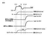
図8に、本実施形態の書き込み時におけるプログラムタイミングチャートを示す。 FIG. 8 shows a program timing chart at the time of writing in this embodiment.
書き込みセルと非書き込みセルはBL電圧で制御する。“0”データの書き込みセルに接続されたビット線には0Vを印加し、t1時から昇圧し“1”データの非書き込みセルに接続されたビット線にはVddを印加する。 Write cells and non-write cells are controlled by the BL voltage. 0 V is applied to the bit line connected to the “0” data write cell, and the voltage is boosted from time t1 and Vdd is applied to the bit line connected to the “1” data non-write cell.
また、ドレイン側選択ゲートSGDには、非書き込みセルに接続されたビット線BLの電圧をセルチャネルに転送するために電圧Vsgを印加し、セルチャネルにVddの転送が完了したところで、Vsgd にする。ソース側選択ゲートSGS(図示略)には0Vを印加する。 A voltage Vsg is applied to the drain side select gate SGD in order to transfer the voltage of the bit line BL connected to the non-write cell to the cell channel, and when the transfer of Vdd to the cell channel is completed, it is set to Vsgd. . 0 V is applied to the source side selection gate SGS (not shown).
これにより選択されたNANDストリング内のチャネルについて、書き込みセルのチャネルを0V、非書き込みセルのチャネルをVddとできる。その後(t4後に)、選択ワード線WLと選択ワード線WLに隣接するワード線WLを含めた3本のワード線WLに書き込み電圧Vpgm(例えば18V)、それ以外のワード線WLにVpass(例えば、10V)を印加する。 As a result, for the channel in the selected NAND string, the channel of the write cell can be set to 0 V, and the channel of the non-write cell can be set to Vdd. Thereafter (after t4), the write voltage Vpgm (for example, 18V) is applied to the three word lines WL including the selected word line WL and the word line WL adjacent to the selected word line WL, and Vpass (for example, to the other word lines WL, for example). 10V) is applied.
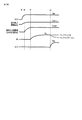
図9及び図10に、ベリファイにおけるプログラムタイミングチャートを示す。 9 and 10 show program timing charts in verification.
図9では、選択ワード線WLのみベリファイを行う。これは、n番目の選択ワード線WLの両隣の(n±1)番目のワード線WLに関してはデータ格納のためではなく、n番目のワード線WLの電荷抜けを防止するためであり、(n±1)番目のワード線WLに接続されたメモリセルの閾値がベリファイレベルを超えているか確認する必要がないためである。それ以上に、ベリファイを選択ワード線WLのみで済ませることができ、高速化に有利である。 In FIG. 9, only the selected word line WL is verified. This is not to store data for the (n ± 1) th word line WL on both sides of the nth selected word line WL, but to prevent charge loss of the nth word line WL. This is because it is not necessary to check whether the threshold value of the memory cell connected to the (± 1) th word line WL exceeds the verify level. In addition, verification can be completed with only the selected word line WL, which is advantageous for speeding up.
具体的には、図9に示すように、t0時から、ドレイン側選択ゲートSGDには、電圧Vsgを印加し、選択ワード線WLには、Vverifyを印加する。t1時から非選択ワード線WLにVreadを印加する。 Specifically, as shown in FIG. 9, from time t0, the voltage Vsg is applied to the drain side select gate SGD, and Vverify is applied to the selected word line WL. Vread is applied to the non-selected word line WL from time t1.
t0後のt1時からビット線BLにはVblを印加し、この昇圧されたVblの電圧が下がるか否かでベリファイパス/フェイルの判定をする。 From t1 after t0, Vbl is applied to the bit line BL, and a verify pass / fail judgment is made based on whether or not the boosted Vbl voltage drops.
t4時からソース側選択ゲートSGS(図示略)には、Vsqを印加する。 From t4, Vsq is applied to the source side selection gate SGS (not shown).
図10では、選択ワード線WLとその両隣のワード線WLに対してベリファイを行う。この場合には、3本のワード線に対してベリファイを行うために、より確実に電荷の横抜けを防止することができる。この場合には、3本のワード線に対してベリファイを行うために、選択ワード線WLの両隣のワード線に接続されたメモリセルの閾値もベリファイレベル以上であることが保障される。したがって、選択ワード線WLに接続されたメモリセルに対してより確実に電荷の横抜けを防止することができる。 In FIG. 10, verification is performed on the selected word line WL and the adjacent word lines WL. In this case, since the verify operation is performed on the three word lines, it is possible to more reliably prevent the electric charge from passing through. In this case, in order to perform verification on the three word lines, it is ensured that the threshold value of the memory cell connected to the word line adjacent to the selected word line WL is also equal to or higher than the verify level. Therefore, it is possible to more reliably prevent electric charges from passing through the memory cells connected to the selected word line WL.
[本実施形態の効果]
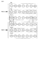
以上により、データ書き込みの高速化をはかり得る不揮発性半導体記憶装置を提供できる。以下、具体的に説明する。図11は、第1の実施形態における書き込みによるn番目及び(n±1)番目のワード線に接続されたメモリセルの閾値分布を示す図であり、図12は、複数ワード線群に接続されたメモリセルに書き込みを行った場合の各メモリセルの閾値分布の状態を示す図である。
[Effect of this embodiment]
As described above, a nonvolatile semiconductor memory device capable of speeding up data writing can be provided. This will be specifically described below. FIG. 11 is a diagram showing threshold distributions of memory cells connected to the nth and (n ± 1) th word lines by writing in the first embodiment, and FIG. 12 is connected to a plurality of word line groups. It is a figure which shows the state of the threshold value distribution of each memory cell at the time of writing in to the memory cell.
本実施形態の不揮発性半導体記憶装置では、n番目及び(n±1)番目のワード線間において、隣接するメモリセルに同一の書き込み電圧VPGM を印加する。このため、例えば、上記のステップS4からステップS6を3回繰り返すことで、図11(b)に示すようなメモリセルの閾値分布となる。 In the nonvolatile semiconductor memory device of this embodiment, the same write voltage V PGM is applied to adjacent memory cells between the nth and (n ± 1) th word lines. For this reason, for example, by repeating step S4 to step S6 three times, the threshold distribution of the memory cell as shown in FIG. 11B is obtained.
このような書き込みを行うことによって、全てのメモリセルを第2の消去状態に書き込むことなく、図12に示すように、着目ワード線WLに接続されたメモリセルにおいてデータの横抜けパターンを取り除くことが可能となる。ここで、図12に示すEは第1の消去状態、Aはベリファイレベルを超えた書き込み状態、Pは、実際にはベリファイは行わないが、閾値がベリファイレベル付近であることが期待される書き込み状態である。 By performing such writing, without removing all the memory cells in the second erased state, as shown in FIG. 12, the data leakage pattern is removed from the memory cells connected to the target word line WL. Is possible. Here, E shown in FIG. 12 is the first erase state, A is the write state exceeding the verify level, and P is the write that is not actually verified but the threshold is expected to be near the verify level. State.
なお、ベリファイについては、n番目のワード線WLに対してのみ行い、(n±1)番目のワード線WLについてはベリファイを行わない。 The verify is performed only for the nth word line WL, and the verify is not performed for the (n ± 1) th word line WL.
このように平面NANDと同様、第2の消去状態に書き込むことなく、初期VPGM、ΔVPGM を大きめに設定しても、閾値分布間のマージンを確保しやすく、書き込みの高速化が期待できる。 As described above, as in the case of the planar NAND, even if the initial V PGM and ΔV PGM are set to be large without writing in the second erase state, it is easy to secure a margin between the threshold distributions, and high-speed writing can be expected.
また、本実施形態で行うベリファイは、n番目のワード線に接続されたメモリセルの閾値電圧が所望の電圧を超えたか否かを判定するものである。先行の不揮発性半導体記憶装置の場合には、第2の消去状態(E’)のベリファイを行う必要があるが、本実施形態では、第2の消去状態(E’)のベリファイを行う必要はない。したがって、図14に示すように、本実施形態の不揮発性半導体記憶装置(図14(b)参照)は、先行の不揮発性半導体記憶装置(図14(a)参照)と比べて、印加するパルス数を低減できる。ここで、図14(a)は、先行の不揮発性半導体記憶装置の書き込み動作を示すタイミングチャート図であり、図14(b)は、本実施形態の不揮発性半導体記憶装置の書き込み動作を示すタイミングチャート図である。 In addition, the verification performed in this embodiment is to determine whether or not the threshold voltage of the memory cell connected to the nth word line has exceeded a desired voltage. In the case of the preceding nonvolatile semiconductor memory device, it is necessary to perform verification of the second erase state (E ′). However, in this embodiment, it is necessary to perform verification of the second erase state (E ′). Absent. Therefore, as shown in FIG. 14, the nonvolatile semiconductor memory device (see FIG. 14B) of the present embodiment applies pulses to be applied compared to the preceding nonvolatile semiconductor memory device (see FIG. 14A). The number can be reduced. Here, FIG. 14A is a timing chart showing the write operation of the preceding nonvolatile semiconductor memory device, and FIG. 14B is a timing showing the write operation of the nonvolatile semiconductor memory device of this embodiment. It is a chart figure.
したがって、先行の不揮発性半導体記憶装置と比べて、本実施形態は、データ書き込みの高速化を図りうる不揮発性半導体記憶装置を提供できる。 Therefore, as compared with the preceding nonvolatile semiconductor memory device, this embodiment can provide a nonvolatile semiconductor memory device capable of speeding up data writing.
但し、nページ(WLn)に書き込みを行った後は、次に書き込み可能なページは(n+3)ページ(WLn+3)になるため、このSLCバッファ方式を用いた場合、2ビット/cellのMLCの1ブロック分のデータを書き込むのに6ブロックが必要となる。 However, after writing to n page (WLn), the next writable page is (n + 3) page (WLn + 3). Therefore, when this SLC buffer method is used, 1 MLC of 2 bits / cell. Six blocks are required to write data for blocks.
より詳しく本実施形態の効果について図13を用いて説明する。図13は、複数のワード線群に書き込みを行った場合のメモリセルの閾値分布の状態を示す模式図である。ここで、n番目乃至(n+2)番目のワード線を1つのワード線群とする。図13では、本実施形態の一例として、2つのワード線群(n番目乃至(n+2)番目のワード線を有する第1のワード線群、(n+3)番目乃至(n+5)番目のワード線を有する第2のワード線群)においてデータの書き込みを行った場合を示す。 The effect of this embodiment will be described in more detail with reference to FIG. FIG. 13 is a schematic diagram showing a threshold distribution state of memory cells when writing is performed on a plurality of word line groups. Here, the nth to (n + 2) th word lines are defined as one word line group. In FIG. 13, as an example of the present embodiment, two word line groups (a first word line group having nth to (n + 2) th word lines, and an (n + 3) th to (n + 5) th word line are included. A case where data is written in the second word line group) is shown.
第1のワード線群について、(n+1)番目のワード線WLを着目ワード線として、その前後のn番目及び(n+2)番目のワード線WLにも同時に書き込みを行う。第2のワード線群について、(n+4)番目のワード線WLを着目ワード線として、その前後の(n+3)番目及び(n+5)番目のワード線WLにも同時に書き込みを行う。 For the first word line group, the (n + 1) th word line WL is used as the target word line, and writing is simultaneously performed to the nth and (n + 2) th wordlines WL before and after the first wordline group. For the second word line group, the (n + 4) th word line WL is set as the target word line, and writing is simultaneously performed on the (n + 3) th and (n + 5) th word lines WL before and after the word line WL.
第1のワード線群における(n+1)番目のワード線と第2のワード線群における(n+4)番目のワード線とに接続されたメモリセルは、本来のデータを格納する部分として使用する。 The memory cells connected to the (n + 1) th word line in the first word line group and the (n + 4) th word line in the second word line group are used as a part for storing original data.
この場合に、(n+2)番目のワード線WL(第1のワード線群)に接続されたメモリセルに対して、(n+3)番目のワード線WL(第2のワード線群)に接続された隣接するメモリセルの関係で、データの横抜けパターンが生じる場合がある。しかし、(n+2)番目と(n+3)番目のワード線WLに接続されたメモリセルは本来のデータを格納する部分ではない。したがって、これらメモリセルの間でデータの横抜けパターンが生じても、本来のデータを格納する部分である(n+1)番目のワード線と(n+4)番目のワード線とに接続されたメモリセルの電荷蓄積層に蓄積された電荷の横抜けを軽減できる。その結果、データの破損などを防止でき、データの信頼性を向上できる。 In this case, the memory cell connected to the (n + 2) th word line WL (first word line group) is connected to the (n + 3) th word line WL (second word line group). There is a case where a data breakthrough pattern occurs due to the relationship between adjacent memory cells. However, the memory cells connected to the (n + 2) th and (n + 3) th word lines WL are not portions for storing original data. Therefore, even if a data breakthrough pattern occurs between these memory cells, the memory cells connected to the (n + 1) th word line and the (n + 4) th word line, which are the parts that store the original data, Bypassing charges accumulated in the charge accumulation layer can be reduced. As a result, data corruption can be prevented and data reliability can be improved.
このように本実施形態によれば、メモリセルアレイのn番目のワード線WLに接続されたメモリセル群にデータを書き込む際に、(n−1)番目のワード線WL及び(n+1)番目のワード線WLに接続されたメモリセル群に同じデータを同時に書き込むことにより、データ書き込みの高速化及びデータ信頼性の向上をはかることができる。 As described above, according to the present embodiment, when data is written to the memory cell group connected to the nth word line WL of the memory cell array, the (n−1) th word line WL and the (n + 1) th word are written. By simultaneously writing the same data to the memory cell group connected to the line WL, the data writing speed can be increased and the data reliability can be improved.
即ち、3本のワード線WLに接続されたメモリセルを用いて、1ページのデータを書き込むため、着目ワード線WLの両側のワード線WLをシールドとして用いることにより、データ信頼性の向上をはかることができる。しかも、書き込みに際しては3本のワード線を同時に選択するのみで良いため、書き込み時間が増大することもない。 That is, since one page of data is written using memory cells connected to the three word lines WL, the data reliability is improved by using the word lines WL on both sides of the word line WL of interest as a shield. be able to. In addition, since it is only necessary to select three word lines at the time of writing, the writing time does not increase.
(第2の実施形態)
次に、第2の実施形態に係わる不揮発性半導体記憶装置を説明する。MLCのチップを用いたSSD(Solid State Drive)においてSLCをバッファとして使用した例を用いて説明する。本実施形態にかかる不揮発性半導体記憶装置は、第1の実施形態に係わる不揮発性半導体記憶装置と構成は同一であるが、動作方法が異なる。したがって、本実施形態では、不揮発性半導体記憶装置の動作方法について詳細に説明する。
(Second Embodiment)
Next, a nonvolatile semiconductor memory device according to the second embodiment will be described. Description will be made using an example in which an SLC is used as a buffer in an SSD (Solid State Drive) using an MLC chip. The nonvolatile semiconductor memory device according to the present embodiment has the same configuration as the nonvolatile semiconductor memory device according to the first embodiment, but the operation method is different. Therefore, in this embodiment, an operation method of the nonvolatile semiconductor memory device will be described in detail.
[不揮発性半導体記憶装置の動作方法]
説明の便宜上、第1の実施形態におけるステップS1からステップS6までのいわゆるSLC書き込みを行い、SLCバッファにデータが書き込まれていることを前提として説明する。
[Operation Method of Nonvolatile Semiconductor Memory Device]
For convenience of explanation, the description will be made on the assumption that so-called SLC writing from step S1 to step S6 in the first embodiment is performed and data is written in the SLC buffer.
ステップSAで、制御回路15は、SLCバッファにデータが書き込まれた2ページ分を選択するようロウデコーダ14、センスアンプ12などを制御する。
In step SA, the
ステップSBで、制御回路15は、センスアンプ12などを制御し、センスアンプ12に2ページ分のデータを読み出し、センスアンプ12内のデータラッチにこれらのデータを保持する。
In step SB, the
ステップSCで、制御回路15は、メモリセルアレイ11内の所望のアドレス信号をロウデコーダ14、センスアンプ12に出力し、データラッチに保持された2ページ分のデータを、所望のアドレスのメモリセルに対してMLC書き込みできるようロウデコーダ14、センスアンプ12、電圧生成回路16などを制御する。
In step SC, the
このステップSAからステップSCを第1の実施形態で書き込まれたブロックに対して行う。すなわち、第1の実施形態で書き込まれたブロックの全てのページがMLC書き込みされるまで、ステップSAからステップSCを繰り返す。 Steps SA to SC are performed on the block written in the first embodiment. That is, step SA to step SC are repeated until all pages of the block written in the first embodiment are written in MLC.
ステップSDで、第1の実施形態で書き込まれたブロックの全てのページがMLC書き込みされたとき、制御回路15は、SLCバッファに書き込まれたブロックのデータを消去する。
In step SD, when all the pages of the block written in the first embodiment are written by MLC, the
なお、ステップSBで、センスアンプ12に2ページ分のデータを読み出し、センスアンプ12内のデータラッチにこれらのデータを保持する際に、読み出した2ページ分のデータを外部入出力端子I/Oを介してメモリコントローラ20に読み出し、その後にECCでエラー訂正を行った後に、ステップSCを行ってもよい。
At step SB, when two pages of data are read out to the
このように、MLCのチップでも高速なデータ書き込みが必要な場合には、SLCをバッファとして使用する。第1の実施形態同様に、本実施形態でも、データ書き込みの高速化をはかり得る不揮発性半導体記憶装置を提供できる。 Thus, when high-speed data writing is required even in the MLC chip, the SLC is used as a buffer. Similar to the first embodiment, this embodiment can also provide a nonvolatile semiconductor memory device capable of increasing the speed of data writing.
(第3の実施形態)
本実施形態の不揮発性半導体記憶装置では、第1及び第2の実施形態に対して、メモリコントローラが、第1の実施形態のように3本のワード線に接続されたメモリセルにデータ書き込みを行う超高速SLCバッファーモード(第1の書き込みモード)と、1本のワード線に接続されたメモリセルの消去状態を、第1の消去状態から第2の消去状態に書き込み、データ書き込みを行う高速SLCバッファーモード(第2の書き込みモード)を選択する点で異なり、その他は同様である。
(Third embodiment)
In the nonvolatile semiconductor memory device of the present embodiment, in contrast to the first and second embodiments, the memory controller writes data to the memory cells connected to the three word lines as in the first embodiment. High-speed SLC buffer mode (first write mode) to be performed and high-speed data writing by writing the erase state of the memory cell connected to one word line from the first erase state to the second erase state It is different in that the SLC buffer mode (second write mode) is selected, and the others are the same.
本実施形態では、メモリコントローラ20は、第1の書き込みモード及び第2の書き込みモードのいずれかを選択する。第1の実施形態にかかる不揮発性半導体記憶装置の動作におけるステップS2で、本実施形態のメモリコントローラ20が、第1モードを選択するとき第1の書き込みモード信号を、第2モードを選択するとき第2の書き込みモード信号を生成する。 In the present embodiment, the memory controller 20 selects either the first write mode or the second write mode. In step S2 in the operation of the nonvolatile semiconductor memory device according to the first embodiment, the memory controller 20 of this embodiment selects the first write mode signal when selecting the first mode, and the second mode. A second write mode signal is generated.
第1の書き込みモードでは、第1の実施形態と同様に、3本のワード線WLに接続されたメモリセルを用いて1ページのデータを書き込む。このモードでは、両隣接ワード線WLにも同時に同じデータを書き込むことによって、3本のワード線WLに接続されたメモリセルの閾値を正に書き戻す必要がなくなる。このため、高速・高信頼性のデータを書き込むことができる。ここでは、両隣接WLをシールドページと呼ぶ。 In the first write mode, one page of data is written using memory cells connected to three word lines WL, as in the first embodiment. In this mode, it is not necessary to write back the threshold values of the memory cells connected to the three word lines WL positively by simultaneously writing the same data to both adjacent word lines WL. Therefore, high-speed and high-reliability data can be written. Here, both adjacent WLs are called shield pages.
第2の書き込みモードでは、図11に示したように、1本のワード線に接続されたメモリセルの消去状態を、第1の消去状態から第2の消去状態に書き込み、データ書き込みを行う。また、この第2の書き込みモードでは、シールドページが不要なことから、第1の書き込みモードで書き込む場合よりも、本来のデータを格納するためのページ数を1/3に削減することができる。また、第2の書き込みモードは、通常のMLCで書き込む場合と比較しても、後述するようにデータの信頼性が高く、かつ、書き込み速度も高速である。 In the second write mode, as shown in FIG. 11, the erase state of the memory cell connected to one word line is written from the first erase state to the second erase state, and data is written. In addition, since the shield page is unnecessary in the second write mode, the number of pages for storing original data can be reduced to 1/3 as compared with the case of writing in the first write mode. In the second write mode, data reliability is high and the write speed is high, as will be described later, as compared with the case of writing by normal MLC.
このように本実施形態によれば、例えばメモリコントローラからの要求が非常に高速な書き込みである場合には、メモリコントローラ20は3本のワード線WLの領域を用いて1ページのデータを書き込む第1の書き込みモードを選択し、メモリコントローラからの要求が第1の書き込みモードと比較して高速な書き込みでない場合には、メモリコントローラ20は第2の書き込みモードを選択する。その結果、要求される書き込み速度に応じて最適な書き込み制御を行うことができる。 As described above, according to the present embodiment, for example, when the request from the memory controller is very high-speed writing, the memory controller 20 writes the data of one page using the areas of the three word lines WL. When one write mode is selected and the request from the memory controller is not a high-speed write compared to the first write mode, the memory controller 20 selects the second write mode. As a result, optimal write control can be performed according to the required write speed.
また、例えばブロックの管理情報など高い信頼性が要求されるデータをメモリセルアレイに書き込む場合には、メモリコントローラ20は第2の書き込みモードを選択する。これにより、このデータはMLC書き込みでなく、SLC書き込みを行うことになり、データの信頼性を向上できる。このように外部メモリコントローラは、用途に応じて書き込みモード信号を生成し、最適な書き込みを行う。 For example, when data that requires high reliability, such as block management information, is written to the memory cell array, the memory controller 20 selects the second write mode. As a result, this data is not MLC written but SLC written, and the reliability of the data can be improved. As described above, the external memory controller generates a write mode signal according to the application and performs optimum writing.
(変形例)
なお、本発明は上述した各実施形態に限定されるものではない。メモリセルアレイの構成は必ずしもBiCSに限るものではなく、電荷蓄積層と制御ゲートを有するメモリセルを基板上に積層した、積層型のメモリセル構造の不揮発性半導体記憶装置に適用することができる。さらに、BiCSの構造も前記図1に何ら限定されるものではなく、仕様に応じて適宜変更可能である。
(Modification)
The present invention is not limited to the above-described embodiments. The configuration of the memory cell array is not necessarily limited to BiCS, and can be applied to a nonvolatile semiconductor memory device having a stacked memory cell structure in which memory cells having a charge storage layer and a control gate are stacked on a substrate. Further, the structure of BiCS is not limited to that shown in FIG. 1, and can be appropriately changed according to the specifications.
また、実施形態ではSLCのデータ書き込みに適用した例で説明したが、MLCのデータ書き込みに適用することも可能である。 In the embodiment, the example is described in which the present invention is applied to SLC data writing. However, the present invention can also be applied to MLC data writing.
本発明のいくつかの実施形態を説明したが、これらの実施形態は、例として提示したものであり、発明の範囲を限定することは意図していない。これら新規な実施形態は、その他の様々な形態で実施されることが可能であり、発明の要旨を逸脱しない範囲で、種々の省略、置き換え、変更を行うことができる。これら実施形態やその変形は、発明の範囲や要旨に含まれると共に、特許請求の範囲に記載された発明とその均等の範囲に含まれる。 Although several embodiments of the present invention have been described, these embodiments are presented by way of example and are not intended to limit the scope of the invention. These novel embodiments can be implemented in various other forms, and various omissions, replacements, and changes can be made without departing from the scope of the invention. These embodiments and modifications thereof are included in the scope and gist of the invention, and are included in the invention described in the claims and the equivalents thereof.
10…BiCSフラッシュメモリ
11…メモリセルアレイ
12…センスアンプ
13…カラムアドレスバッファ/カラムデコーダ
14…ロウデコーダ
15…制御回路
16…電圧生成回路
17…パワーオン検出回路
18…ロウアドレスバッファ
19…入出力バッファ
20…メモリコントローラ
31…半導体基板
32…ソース拡散層
33…トンネル絶縁膜
34…電荷蓄積層
35…ブロック絶縁膜
36…制御ゲート
DESCRIPTION OF
Claims (6)
前記メモリセルアレイのn番目(nは自然数)のワード線と電気的に接続された第1メモリセル及び第2メモリセルにデータを書き込む際に、前記第1メモリセルと電気的に接続される第1ビット線に第1電圧を、前記第2メモリセルと電気的に接続される第2ビット線に前記第1電圧よりも高い第2電圧を印加したまま、(n−1)番目及び(n+1)番目のワード線にn番目のワード線と同一の書き込み電圧を一括して印加するよう制御する制御回路と、
を具備したことを特徴とする不揮発性半導体記憶装置。 A plurality of word lines that are stacked on a semiconductor substrate, are connected to the plurality of memory cells having a charge storage layer, respectively, and a Rume Moriseruarei have charge storage layer between adjacent memory cells in series,
When data is written in the first memory cell and the second memory cell electrically connected to the nth (n is a natural number) word line of the memory cell array, the first memory cell electrically connected to the first memory cell With the first voltage applied to one bit line and the second voltage higher than the first voltage applied to the second bit line electrically connected to the second memory cell, the (n−1) th and (n + 1) th A control circuit that controls to apply the same write voltage to the nth word line to the nth word line in a batch ;
A non-volatile semiconductor memory device comprising:
前記n番目のワード線に接続された第1メモリセルの閾値電圧が所望の正の電圧を超えるまで、前記n番目及び前記(n±1)番目のワード線に書き込み電圧を一括して印加することを特徴とする請求項1記載の不揮発性半導体記憶装置。 The control circuit performs verification on the first memory cell and the second memory cell connected to the nth word line,
A write voltage is collectively applied to the nth and (n ± 1) word lines until the threshold voltage of the first memory cell connected to the nth word line exceeds a desired positive voltage. The nonvolatile semiconductor memory device according to claim 1.
ベリファイフェイルしたメモリセルと電気的に接続されたビット線に書き込み電圧を印加することを特徴とする請求項2又は3記載の不揮発性半導体記憶装置。 Before SL control circuit, according to the result of the verification, the non-writing voltage is applied to the memory cell and electrically connected to the bit line to verify pass,
4. The nonvolatile semiconductor memory device according to claim 2, wherein a write voltage is applied to a bit line electrically connected to the verify-failed memory cell.
前記半導体基板上に柱状に形成された活性層と、
前記活性層の側壁面を囲むようにトンネル絶縁膜,電荷蓄積層,及びブロック絶縁膜が形成されたゲート絶縁膜部と、
前記ゲート絶縁膜部の側壁面を囲むように形成されて、且つ前記半導体基板上に複数の層間絶縁膜と複数の導電層が交互に積層された積層構造部と
を有し、
前記活性層,トンネル絶縁膜,電荷蓄積層,ブロック絶縁膜,及び導電層を含むトランジスタで前記メモリセルを構成したものであることを特徴とする請求項1乃至4の何れか1項に記載の不揮発性半導体記憶装置。 The memory cell array includes:
An active layer formed in a columnar shape on the semiconductor substrate;
A gate insulating film portion in which a tunnel insulating film, a charge storage layer, and a block insulating film are formed so as to surround a side wall surface of the active layer;
A multilayer structure portion formed so as to surround a side wall surface of the gate insulating film portion, and a plurality of interlayer insulating films and a plurality of conductive layers alternately stacked on the semiconductor substrate;
5. The memory cell according to claim 1, wherein the memory cell includes a transistor including the active layer, a tunnel insulating film, a charge storage layer, a block insulating film, and a conductive layer. Nonvolatile semiconductor memory device.
前記第1メモリセル及び前記第2メモリセルにデータを書き込む際に、前記第1ビット線に前記第1電圧を、前記第2ビット線に前記第2電圧を印加したまま、(n−1)番目及び(n+1)番目のワード線にn番目のワード線と同一の書き込み電圧を一括して印加する第1の書き込みモードと、
前記第1メモリセル及び前記第2メモリセルにデータを書き込む際に、前記第1メモリセル及び第2メモリセルの閾値電圧を、負の閾値電圧を有する第1消去状態から正の閾値電圧を有する第2消去状態へと遷移させた後、前記第1ビット線に前記第1電圧を、前記第2ビット線に前記第2電圧を印加したまま、前記n番目のワード線に書き込み電圧を印加する第2の書き込みモードと
のいずれかを選択することを特徴とする請求項1乃至5の何れか1項に記載の不揮発性半導体記憶装置。 The control circuit, depending on the required writing speed,
When writing data to the first memory cell and the second memory cell, the first voltage is applied to the first bit line and the second voltage is applied to the second bit line. A first write mode in which the same write voltage as that of the nth word line is collectively applied to the nth and (n + 1) th word lines;
When writing data to the first memory cell and the second memory cell, the threshold voltage of the first memory cell and the second memory cell is changed from a first erase state having a negative threshold voltage to a positive threshold voltage. After the transition to the second erase state, the write voltage is applied to the nth word line while the first voltage is applied to the first bit line and the second voltage is applied to the second bit line. The nonvolatile semiconductor memory device according to claim 1, wherein one of the second write mode and the second write mode is selected.
Priority Applications (3)
| Application Number | Priority Date | Filing Date | Title |
|---|---|---|---|
| JP2010212720A JP5259666B2 (en) | 2010-09-22 | 2010-09-22 | Nonvolatile semiconductor memory device |
| KR1020110023771A KR20120031113A (en) | 2010-09-22 | 2011-03-17 | Nonvolatile semiconductor memory device |
| US13/157,603 US8593872B2 (en) | 2010-09-22 | 2011-06-10 | Nonvolatile semiconductor memory device capable of speeding up data write |
Applications Claiming Priority (1)
| Application Number | Priority Date | Filing Date | Title |
|---|---|---|---|
| JP2010212720A JP5259666B2 (en) | 2010-09-22 | 2010-09-22 | Nonvolatile semiconductor memory device |
Publications (2)
| Publication Number | Publication Date |
|---|---|
| JP2012069200A JP2012069200A (en) | 2012-04-05 |
| JP5259666B2 true JP5259666B2 (en) | 2013-08-07 |
Family
ID=45817666
Family Applications (1)
| Application Number | Title | Priority Date | Filing Date |
|---|---|---|---|
| JP2010212720A Active JP5259666B2 (en) | 2010-09-22 | 2010-09-22 | Nonvolatile semiconductor memory device |
Country Status (3)
| Country | Link |
|---|---|
| US (1) | US8593872B2 (en) |
| JP (1) | JP5259666B2 (en) |
| KR (1) | KR20120031113A (en) |
Cited By (1)
| Publication number | Priority date | Publication date | Assignee | Title |
|---|---|---|---|---|
| US10049760B2 (en) | 2016-09-06 | 2018-08-14 | Toshiba Memory Corporation | Programming and verification methods for three-dimensional memory device |
Families Citing this family (24)
| Publication number | Priority date | Publication date | Assignee | Title |
|---|---|---|---|---|
| CN103119656A (en) * | 2010-09-24 | 2013-05-22 | 株式会社东芝 | Nonvolatile semiconductor memory device |
| KR101893562B1 (en) * | 2012-01-09 | 2018-10-04 | 삼성전자주식회사 | Nonvolatile memory device and program method thereof |
| KR101913331B1 (en) * | 2012-01-19 | 2018-10-30 | 삼성전자주식회사 | Nonvolatile memory device, novolatile memory system, program method thereof, and operation method of controller controlling the same |
| US9099202B2 (en) | 2012-11-06 | 2015-08-04 | Sandisk Technologies Inc. | 3D stacked non-volatile storage programming to conductive state |
| US9466382B2 (en) | 2012-11-14 | 2016-10-11 | Sandisk Technologies Llc | Compensation for sub-block erase |
| US8830717B2 (en) | 2012-11-29 | 2014-09-09 | Sandisk Technologies Inc. | Optimized configurable NAND parameters |
| US8988941B2 (en) | 2012-12-18 | 2015-03-24 | SanDisk Tehcnologies Inc. | Select transistor tuning |
| KR102090589B1 (en) * | 2013-01-14 | 2020-03-18 | 삼성전자주식회사 | Method of storing data in a nonvolatile memory device and method of testing a nonvolatile memory device |
| US9218890B2 (en) | 2013-06-03 | 2015-12-22 | Sandisk Technologies Inc. | Adaptive operation of three dimensional memory |
| KR102175039B1 (en) | 2013-06-25 | 2020-11-05 | 삼성전자주식회사 | Method of writing data in non-volatile memory device |
| TWI573148B (en) | 2013-08-02 | 2017-03-01 | 東芝股份有限公司 | A controller, a memory system, and a memory device |
| US9324438B2 (en) | 2013-08-05 | 2016-04-26 | Jonker Llc | Method of operating incrementally programmable non-volatile memory |
| CN104425020A (en) * | 2013-08-23 | 2015-03-18 | 慧荣科技股份有限公司 | Method for accessing storage unit in flash memory and device using the same |
| US9142324B2 (en) | 2013-09-03 | 2015-09-22 | Sandisk Technologies Inc. | Bad block reconfiguration in nonvolatile memory |
| KR20150060144A (en) * | 2013-11-26 | 2015-06-03 | 삼성전자주식회사 | Method of operating nonvolatile memory device |
| US9218886B2 (en) | 2013-12-10 | 2015-12-22 | SanDisk Technologies, Inc. | String dependent parameter setup |
| KR102128466B1 (en) * | 2014-04-14 | 2020-06-30 | 삼성전자주식회사 | Memory System, Method of Programming the Memory System and Method of Testing the Memory System |
| US9613713B2 (en) * | 2014-09-16 | 2017-04-04 | Kabushiki Kaisha Toshiba | Semiconductor memory device |
| JP2016062623A (en) * | 2014-09-16 | 2016-04-25 | 株式会社東芝 | Semiconductor memory device |
| US9691473B2 (en) | 2015-09-22 | 2017-06-27 | Sandisk Technologies Llc | Adaptive operation of 3D memory |
| US9401216B1 (en) | 2015-09-22 | 2016-07-26 | Sandisk Technologies Llc | Adaptive operation of 3D NAND memory |
| JP2017162526A (en) | 2016-03-07 | 2017-09-14 | 東芝メモリ株式会社 | Memory device |
| US9916901B1 (en) * | 2017-01-26 | 2018-03-13 | Micron Technology, Inc. | Memory device including multiple gate-induced drain leakage current generator circuits |
| JP2018147535A (en) * | 2017-03-07 | 2018-09-20 | 東芝メモリ株式会社 | Semiconductor memory device and memory system |
Family Cites Families (19)
| Publication number | Priority date | Publication date | Assignee | Title |
|---|---|---|---|---|
| JP3576763B2 (en) * | 1997-08-21 | 2004-10-13 | 株式会社東芝 | Semiconductor storage device |
| JPH11162199A (en) * | 1997-11-25 | 1999-06-18 | Hitachi Ltd | Semiconductor storage device |
| JP2000236031A (en) * | 1999-02-16 | 2000-08-29 | Toshiba Corp | Nonvolatile semiconductor memory device |
| JP3983969B2 (en) * | 2000-03-08 | 2007-09-26 | 株式会社東芝 | Nonvolatile semiconductor memory device |
| JP3709126B2 (en) * | 2000-07-05 | 2005-10-19 | シャープ株式会社 | Erase method for nonvolatile semiconductor memory device |
| JP3702229B2 (en) * | 2002-01-16 | 2005-10-05 | 株式会社東芝 | Semiconductor memory device |
| CN101213614B (en) * | 2005-03-31 | 2012-05-16 | 桑迪士克股份有限公司 | Erasing non-volatile memory using individual verification and additional erasing of subsets of memory cells |
| JP4796126B2 (en) * | 2005-03-31 | 2011-10-19 | サンディスク コーポレイション | Soft programming of non-volatile memory by individually verifying and further soft programming a subset of memory cells |
| JP2007257739A (en) * | 2006-03-23 | 2007-10-04 | Toshiba Corp | Nonvolatile semiconductor memory device |
| JP5019198B2 (en) * | 2006-06-29 | 2012-09-05 | 株式会社東芝 | Semiconductor memory device |
| JP5142692B2 (en) * | 2007-12-11 | 2013-02-13 | 株式会社東芝 | Nonvolatile semiconductor memory device |
| US7633804B2 (en) * | 2008-03-20 | 2009-12-15 | Micron Technology, Inc. | Adjusting programming or erase voltage pulses in response to the number of programming or erase failures |
| JP2009230818A (en) * | 2008-03-24 | 2009-10-08 | Toshiba Corp | Semiconductor storage device |
| JP2009266946A (en) * | 2008-04-23 | 2009-11-12 | Toshiba Corp | Three-dimensional stacked nonvolatile semiconductor memory |
| JP2009301607A (en) * | 2008-06-10 | 2009-12-24 | Toshiba Corp | Nonvolatile semiconductor memory device and method for controlling the same |
| KR101468099B1 (en) * | 2008-07-24 | 2014-12-03 | 삼성전자주식회사 | Program method of nonvolatile memory device |
| JP2010118580A (en) * | 2008-11-14 | 2010-05-27 | Toshiba Corp | Non-volatile semiconductor memory device |
| JP5275052B2 (en) * | 2009-01-08 | 2013-08-28 | 株式会社東芝 | Nonvolatile semiconductor memory device |
| JP2010199235A (en) * | 2009-02-24 | 2010-09-09 | Toshiba Corp | Nonvolatile semiconductor storage device |
-
2010
- 2010-09-22 JP JP2010212720A patent/JP5259666B2/en active Active
-
2011
- 2011-03-17 KR KR1020110023771A patent/KR20120031113A/en not_active Ceased
- 2011-06-10 US US13/157,603 patent/US8593872B2/en active Active
Cited By (1)
| Publication number | Priority date | Publication date | Assignee | Title |
|---|---|---|---|---|
| US10049760B2 (en) | 2016-09-06 | 2018-08-14 | Toshiba Memory Corporation | Programming and verification methods for three-dimensional memory device |
Also Published As
| Publication number | Publication date |
|---|---|
| US20120069667A1 (en) | 2012-03-22 |
| JP2012069200A (en) | 2012-04-05 |
| US8593872B2 (en) | 2013-11-26 |
| KR20120031113A (en) | 2012-03-30 |
Similar Documents
| Publication | Publication Date | Title |
|---|---|---|
| JP5259666B2 (en) | Nonvolatile semiconductor memory device | |
| US8570802B2 (en) | Nonvolatile semiconductor memory device capable of speeding up write operation | |
| TWI656534B (en) | Memory device | |
| US9799406B2 (en) | Memory system | |
| US7539061B2 (en) | Method of programming flash memory device | |
| CN110085272B (en) | Semiconductor memory device | |
| CN109817266B (en) | Non-volatile storage device and erasing method thereof | |
| CN111725211B (en) | Semiconductor storage device | |
| JP2010009733A (en) | Nonvolatile semiconductor memory device | |
| JP2015176623A (en) | Semiconductor memory device and memory controller | |
| CN112530486B (en) | Semiconductor memory device | |
| US11709629B2 (en) | Nonvolatile memory device | |
| JP2011198419A (en) | Nonvolatile semiconductor memory device and write method thereof | |
| US20140063972A1 (en) | Semiconductor storage device | |
| JP2014063552A (en) | Semiconductor memory device | |
| JP2012160222A (en) | Nonvolatile semiconductor memory device | |
| JP2020047321A (en) | Semiconductor storage device | |
| US8867273B2 (en) | Non-volatile semiconductor memory device and method of writing data therein | |
| JP2010040125A (en) | Erasing method in nonvolatile semiconductor memory device | |
| US8929144B2 (en) | Nonvolatile semiconductor memory device | |
| TWI858355B (en) | Semiconductor memory devices | |
| US20130163329A1 (en) | Memory system | |
| TWI894766B (en) | semiconductor memory devices | |
| US20250157542A1 (en) | Non-volatile memory device and programming method | |
| JP2013200924A (en) | Nonvolatile semiconductor memory device |
Legal Events
| Date | Code | Title | Description |
|---|---|---|---|
| A621 | Written request for application examination |
Free format text: JAPANESE INTERMEDIATE CODE: A621 Effective date: 20120809 |
|
| A977 | Report on retrieval |
Free format text: JAPANESE INTERMEDIATE CODE: A971007 Effective date: 20121212 |
|
| A131 | Notification of reasons for refusal |
Free format text: JAPANESE INTERMEDIATE CODE: A131 Effective date: 20121218 |
|
| A521 | Request for written amendment filed |
Free format text: JAPANESE INTERMEDIATE CODE: A523 Effective date: 20130218 |
|
| TRDD | Decision of grant or rejection written | ||
| A01 | Written decision to grant a patent or to grant a registration (utility model) |
Free format text: JAPANESE INTERMEDIATE CODE: A01 Effective date: 20130402 |
|
| A61 | First payment of annual fees (during grant procedure) |
Free format text: JAPANESE INTERMEDIATE CODE: A61 Effective date: 20130424 |
|
| FPAY | Renewal fee payment (event date is renewal date of database) |
Free format text: PAYMENT UNTIL: 20160502 Year of fee payment: 3 |
|
| R151 | Written notification of patent or utility model registration |
Ref document number: 5259666 Country of ref document: JP Free format text: JAPANESE INTERMEDIATE CODE: R151 |
|
| S111 | Request for change of ownership or part of ownership |
Free format text: JAPANESE INTERMEDIATE CODE: R313111 |
|
| R350 | Written notification of registration of transfer |
Free format text: JAPANESE INTERMEDIATE CODE: R350 |
|
| S111 | Request for change of ownership or part of ownership |
Free format text: JAPANESE INTERMEDIATE CODE: R313111 |
|
| R350 | Written notification of registration of transfer |
Free format text: JAPANESE INTERMEDIATE CODE: R350 |