JP5259659B2 - Electronics - Google Patents
Electronics Download PDFInfo
- Publication number
- JP5259659B2 JP5259659B2 JP2010191766A JP2010191766A JP5259659B2 JP 5259659 B2 JP5259659 B2 JP 5259659B2 JP 2010191766 A JP2010191766 A JP 2010191766A JP 2010191766 A JP2010191766 A JP 2010191766A JP 5259659 B2 JP5259659 B2 JP 5259659B2
- Authority
- JP
- Japan
- Prior art keywords
- pad
- detection
- bump bonding
- insulating
- electronic device
- Prior art date
- Legal status (The legal status is an assumption and is not a legal conclusion. Google has not performed a legal analysis and makes no representation as to the accuracy of the status listed.)
- Expired - Fee Related
Links
Images


Classifications
-
- G—PHYSICS
- G01—MEASURING; TESTING
- G01R—MEASURING ELECTRIC VARIABLES; MEASURING MAGNETIC VARIABLES
- G01R31/00—Arrangements for testing electric properties; Arrangements for locating electric faults; Arrangements for electrical testing characterised by what is being tested not provided for elsewhere
- G01R31/28—Testing of electronic circuits, e.g. by signal tracer
- G01R31/2801—Testing of printed circuits, backplanes, motherboards, hybrid circuits or carriers for multichip packages [MCP]
- G01R31/2818—Testing of printed circuits, backplanes, motherboards, hybrid circuits or carriers for multichip packages [MCP] using test structures on, or modifications of, the card under test, made for the purpose of testing, e.g. additional components or connectors
-
- G—PHYSICS
- G01—MEASURING; TESTING
- G01R—MEASURING ELECTRIC VARIABLES; MEASURING MAGNETIC VARIABLES
- G01R31/00—Arrangements for testing electric properties; Arrangements for locating electric faults; Arrangements for electrical testing characterised by what is being tested not provided for elsewhere
- G01R31/50—Testing of electric apparatus, lines, cables or components for short-circuits, continuity, leakage current or incorrect line connections
- G01R31/66—Testing of connections, e.g. of plugs or non-disconnectable joints
- G01R31/68—Testing of releasable connections, e.g. of terminals mounted on a printed circuit board
-
- G—PHYSICS
- G01—MEASURING; TESTING
- G01R—MEASURING ELECTRIC VARIABLES; MEASURING MAGNETIC VARIABLES
- G01R31/00—Arrangements for testing electric properties; Arrangements for locating electric faults; Arrangements for electrical testing characterised by what is being tested not provided for elsewhere
- G01R31/50—Testing of electric apparatus, lines, cables or components for short-circuits, continuity, leakage current or incorrect line connections
- G01R31/66—Testing of connections, e.g. of plugs or non-disconnectable joints
- G01R31/70—Testing of connections between components and printed circuit boards
- G01R31/71—Testing of solder joints
Landscapes
- Physics & Mathematics (AREA)
- General Physics & Mathematics (AREA)
- Engineering & Computer Science (AREA)
- Computer Hardware Design (AREA)
- Microelectronics & Electronic Packaging (AREA)
- General Engineering & Computer Science (AREA)
- Electric Connection Of Electric Components To Printed Circuits (AREA)
- Supply And Installment Of Electrical Components (AREA)
- Wire Bonding (AREA)
Description
本発明の実施形態は、電子機器に関する。 Embodiments described herein relate generally to an electronic apparatus.
内部に半導体チップが搭載された半導体パッケージ、または、抵抗やキャパシタ等のチップ型受動部品である電子部品などが複数実装されてなる電子機器は、近年、高機能化および多機能化が求められている。この要求により、半導体チップの高集積化、大規模化が進んでいる。これに伴い、半導体パッケージと回路基板とを接続するはんだバンプなどの電気的接合部の数は大幅に増加している。また、各電気的接合部のサイズは小さくなる傾向にある。従って、半導体パッケージに繰り返し生じる温度変動、曲げ、衝撃、および振動などによって、接合部が破断されることが問題になっている。 2. Description of the Related Art In recent years, electronic devices in which a semiconductor package having a semiconductor chip mounted therein or a plurality of electronic components that are chip-type passive components such as resistors and capacitors have been mounted are required to have higher functionality and more functionality. Yes. Due to this demand, higher integration and larger scale of semiconductor chips are progressing. Along with this, the number of electrical joints such as solder bumps connecting the semiconductor package and the circuit board has greatly increased. Moreover, the size of each electrical joint tends to be small. Therefore, there is a problem that the joint portion is broken by temperature fluctuation, bending, impact, vibration, and the like that are repeatedly generated in the semiconductor package.
このような問題に対し、半導体パッケージが有する抵抗値検出部が、検出用接合部の熱疲労破断による抵抗値の上昇を検出することによって、熱疲労破断を未然に防ぐ手法が知られている。 In order to solve such a problem, a technique is known in which a resistance detection unit included in a semiconductor package detects an increase in resistance value due to thermal fatigue fracture of a detection joint, thereby preventing thermal fatigue fracture.
しかしながら、従来技術では、精度よく接合部の破断を検出できない場合があった。通常、検出用接合部は電子部品の四隅位置に配置され、他の接合部よりも低寿命になるように設計されている。しかし、材料物性や接合部形状のばらつき、検出用接合部と電極パッド界面の大部分が破断しても例えば検出用接合部の中央付近に破断しない部分が残る場合があることなどから、検出用接合部の破断を検出する前に、破断を事前に予測したい接合部が破断する可能性があった。 However, in the prior art, there is a case where the fracture of the joint cannot be detected with high accuracy. Normally, the detection joints are arranged at the four corner positions of the electronic component, and are designed to have a shorter lifetime than the other joints. However, even if the physical properties of the material and the shape of the joint part vary, and the majority of the interface between the detection joint part and the electrode pad breaks, for example, a part that does not break may remain near the center of the joint part for detection. Before detecting the breakage of the joint portion, there is a possibility that the joint portion for which the breakage is predicted in advance may break.
実施形態の電子機器は、回路基板と、電子部品と、前記回路基板上に形成された第1パッドと、前記電子部品上に形成された第2パッドと、前記第1パッドと前記第2パッドとを接合する接合部と、前記第1パッドおよび前記第2のパッドの少なくとも一方と、前記接合部とを含む接続経路の電気特性を検出する検出部と、を備え、前記第1パッドおよび前記第2パッドの少なくとも一方は、前記接合部との接触領域の一部に絶縁部が形成されている。 An electronic apparatus according to an embodiment includes a circuit board, an electronic component, a first pad formed on the circuit board, a second pad formed on the electronic component, the first pad, and the second pad. A detection unit that detects an electrical characteristic of a connection path including at least one of the first pad and the second pad, and the bonding unit, and the first pad and the second pad At least one of the second pads has an insulating portion formed in a part of a contact area with the joint portion.
以下に添付図面を参照して、この発明にかかる電子機器の好適な実施形態を詳細に説明する。 Exemplary embodiments of an electronic device according to the present invention will be described below in detail with reference to the accompanying drawings.
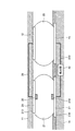
(第1の実施形態)
図1は、第1の実施形態の電子機器を模式的に示す断面図である。図2は、第1の実施形態の検出用バンプ接合部周辺の断面図である。図3は、回路基板上に形成された検出用バンプ接合部のパッドの形状を示す図である。
(First embodiment)
FIG. 1 is a cross-sectional view schematically showing the electronic apparatus of the first embodiment. FIG. 2 is a cross-sectional view of the vicinity of the detection bump bonding portion according to the first embodiment. FIG. 3 is a diagram showing the shape of the pad of the detection bump bonding portion formed on the circuit board.
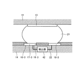
図1に示すように、第1の実施形態の電子機器は、電子部品11と、回路基板14と、バンプ接合部20と、検出用バンプ接合部21とを備えている。バンプ接合部20および検出用バンプ接合部21は、例えばはんだバンプとすることができる。
As shown in FIG. 1, the electronic apparatus according to the first embodiment includes an
電子部品11は、一方の表面に電子部品側パッド12、13が形成されている。電子部品は、例えば、BGA型半導体パッケージである。図1では、半導体パッケージのチップ41を含む電子部品11の例が示されている。
As for the
一方、回路基板14は、例えばFR−4基板であり、一方の表面にパッド15、16が形成されている。電子部品11と回路基板14は、電子部品側パッド12、13、バンプ接合部20、検出用バンプ接合部21、および、パッド15、16によって接続されている。
On the other hand, the
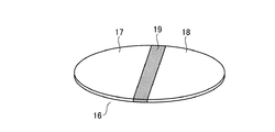
図2に示すように、電子部品11の四隅位置では、電子部品側パッド13と検出用バンプ接合部21とパッド16とが、電子部品11と回路基板14とを機械的に接続している。図2および図3に示すように、パッド16は、その外周に形成された電極部17と電極部18と、電極部17と電極部18とを絶縁する絶縁部19とで構成される。絶縁部19は、例えばソルダーレジストで被覆される絶縁体から形成される。例えば、電極部17と電極部18と絶縁部19と検出用バンプ接合部21は以下のようにして形成することができる。
As shown in FIG. 2, at the four corner positions of the
回路基板14の製造工程において、エッチングで、回路基板上に電極部17および電極部18を含むパターンを形成した後、ソルダーレジストを、パッド等の部分を除いて回路基板14に塗布する。その際、ソルダーレジストを電極部17と電極部18間に塗布し、絶縁部19を形成する。例えば、絶縁部19の幅は、パッド16の直径の50%以下である。バンプ接合部20と検出用バンプ接合部21が形成されている電子部品11を、検出用バンプ21がパッド16上に、バンプ接合部20がそれぞれ対応するパッド上に位置するように、回路基板14上に搭載し、リフロー工程ではんだが熱によって溶融することではんだ付けされ、検出用バンプ21と回路基板14は、電極部17と電極部18で電気的および物理的に接続される。
In the manufacturing process of the
電極部17と電極部18は、絶縁部19を挟んで、互いに離間しており、それぞれが回路基板14上に形成された電気特性値を測定するための配線22に電気的に接続されている。配線22、電極部17、検出用バンプ接合部21、および電極部18の順に導電する接続経路には、検出部42が接続される。検出部42は、この接続経路の電気特性値を測定し、測定した電気特性値に基づいて検出用バンプ接合部21の破断を検出する。検出部42は、電気特性値として例えば電気抵抗値を測定する。そして、検出部42は、例えば測定した電気抵抗値が所定レベルを超えたときに、検出用バンプ接合部21が破断したことを示す信号を出力する。図4は、接続経路が破断する前後の電気抵抗値の時間的変化を模式的に示したものであり、縦軸は電気抵抗値、横軸は時間を示している。この図4では、時刻t=t0において接続経路が破断し、急激に電気抵抗値が上昇したことを模式的に示している。
The
電気特性値は電気抵抗値に限られず、値の変化から検出用バンプ接合部21の破断を検出可能なものであれば、電流値、電圧値などのあらゆる特性値を適用できる。また、図2では、回路基板14が検出部42を含むように記載しているが、回路基板14の外部に検出部42を備えるように構成してもよい。
The electric characteristic value is not limited to the electric resistance value, and any characteristic value such as a current value and a voltage value can be applied as long as the breakage of the detection
配線22は、回路基板14上に形成されているため、電子部品11の従来の回路設計を変更することなく、本実施形態の適用が可能である。
Since the
例えば電源オン/オフによる温度変動に伴い、検出用バンプ接合部21に繰返し熱応力が生じ、検出用バンプ接合部21が破断し、電極部17または電極部18と検出用バンプ接合部21の接続が破断する。これにより電気抵抗値を測定するための接続経路が破断すると、検出部42で測定される電気抵抗値は上昇する。このため、検出部42での電気抵抗値の測定により、検出用バンプ接合部21の破断が検出される。
For example, a thermal stress is repeatedly generated in the detection
一般的に、バンプ接合部で繰返し熱応力によって生じる熱疲労き裂は、電極と接合部の界面近傍の外縁部から発生し、中央に向かって進展する。本実施形態における検出用バンプ接合部21では、中央部分に絶縁部19が形成されているため、き裂が中央に達しなくても電気的に破断する。すなわち、検出用バンプ接合部21の破断および破断の検出が早まることになる。
In general, a thermal fatigue crack caused by repeated thermal stress at a bump joint portion is generated from an outer edge portion near the interface between the electrode and the joint portion, and propagates toward the center. In the detection
また、電子部品11のコーナー直下で回路基板14の曲率が特徴的に変化するため、電子部品11のコーナー直下に近い四隅位置に配置された検出用バンプ接合部21への負荷は、それより内側に配置されているバンプ接合部20に比べ大きく、低寿命になる。なお、検出用バンプ接合部21を配置する部分は、電子部品11の角部(コーナー)に近い四隅に限られるものではなく、電子部品11の周縁部の少なくとも一部に検出用バンプ接合部21を配置すればよい。検出用バンプ接合部21をバンプ接合部20より低寿命にする設計手法としては、他にも多様な方法を適用できる。例えば電子部品11が半導体パッケージの場合には、チップコーナー直下付近(図1の例ではチップ41のコーナー直下付近)に検出用バンプ接合部21を配置してもよい。
In addition, since the curvature of the
絶縁部19を形成している絶縁体の熱膨張係数を、検出用バンプ接合部21の熱膨張係数より大きくなるように構成してもよい。例えば、絶縁部19をソルダーレジストとし、検出用バンプ接合部21をはんだバンプとすることにより、絶縁部19の熱膨張係数を、検出用バンプ接合部21の熱膨張係数より大きくすることができる。この場合、高温時に、絶縁部19と検出用バンプ接合部21の熱膨張差により、検出用バンプ接合部21が上方向に押し上げられる。
You may comprise so that the thermal expansion coefficient of the insulator which forms the insulating
これにより、検出用バンプ接合部21の破断を加速させ、検出用バンプ接合部21の破断が生じた後に、電極部17または電極部18と検出用バンプ接合部21の間の電気的な導通を完全に切断し、検出用バンプ接合部21の破断面同士の接触によって電気的に導通することを防止する効果が得られる。すなわち、破断が生じた後に接触が残ることにより、破断を適切に検出できないことを回避可能となる。
As a result, the breakage of the detection
このような設計では、検出用バンプ接合部21は、バンプ接合部20に比べ低寿命となり、バンプ接合部20が破断する前に検出用バンプ接合部21の破断が検出される。すなわち、検出部42が電気抵抗値の測定によって検出用バンプ接合部21の破断を検出することにより、バンプ接合部20の破断を事前に予測することができる。
In such a design, the detection
電極部17と検出用バンプ接合部21との間と、電極部18と検出用バンプ接合部21との間の接続面積によって、破断検出の時期を調節することが可能である。両者の面積は等しくてもよいし異なっていてもよい。両者の面積が異なる場合には、面積が小さい方で破断が生じやすくなる。この場合、電極部17と電極部18のうち、いずれか一方と検出用バンプ接合部21との接続が破断すれば、もう一方は接続が破断していなくても破断が検出される。このため、電子部品11と検出用バンプ接合部21と回路基板14が機械的には接続された状態で、破断を検出することができる。
The break detection timing can be adjusted by the connection area between the
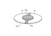
(第1の実施形態の変形例1)
次に、第1の実施形態の変形例1について説明する。図5は、第1の実施形態の変形例1の電子機器における検出用バンプ接合部周辺の断面図である。図6は、第1の実施形態の変形例1のパッド16−2の形状を示す図である。なお、本変形例の説明では、第1の実施形態の電子機器と異なる箇所について説明する。
(Modification 1 of the first embodiment)
Next, Modification 1 of the first embodiment will be described. FIG. 5 is a cross-sectional view of the periphery of the detection bump bonding portion in the electronic apparatus according to the first modification of the first embodiment. FIG. 6 is a diagram illustrating the shape of the pad 16-2 according to the first modification of the first embodiment. In the description of the present modification, parts different from the electronic device according to the first embodiment will be described.
図5と図6に示すように、本変形例の電子機器は、第1の実施形態の電子機器と比較して、絶縁部19の形状が異なる。本変形例では、絶縁部19は、電極部17と電極部18の間のライン状の絶縁部19aと、電極部17および電極部18と絶縁部19aの上の中央に円形状に形成された絶縁部19bとから構成される。
As shown in FIGS. 5 and 6, the electronic device of the present modification is different in the shape of the insulating
本変形例では、絶縁部19bを形成したことで、いずれの方向でも検出用バンプ接合部21の外縁から絶縁部19bまでの距離が短くなる。このため、パッド16−2の配置方向に関わらず、破断の検出を早める効果がある。
In this modification, since the insulating
(第1の実施形態の変形例2)
次に、第1の実施形態の変形例2について説明する。図7は、第1の実施形態の変形例2の電子機器における検出用バンプ接合部周辺の断面図である。図8は、第1の実施形態の変形例2のパッド16−3の形状を示す図である。なお、この変形例の説明では、第1の実施形態の電子機器と異なる箇所について説明する。
(Modification 2 of the first embodiment)
Next, Modification 2 of the first embodiment will be described. FIG. 7 is a cross-sectional view of the periphery of the detection bump bonding portion in the electronic device of Modification 2 of the first embodiment. FIG. 8 is a diagram illustrating the shape of the pad 16-3 according to the second modification of the first embodiment. In the description of this modification, parts different from the electronic device of the first embodiment will be described.
図7と図8に示すように、本変形例の電子機器は、第1の実施形態の電子機器と比較して、回路基板14上の電極部17−3、18−3と絶縁部19−3の形状が異なる。本変形例では、電極部17−3と電極部18−3が、同心円を2つに分割した形状になっている。電極部17−3および電極部18−3は、例えば1つの電極からライン状切欠部とその中央に円形状の切欠部を設けることで形成することができる。本変形例では、電極部17−3と電極部18−3との間に、円形から電極の外縁までラインが延びた形状の絶縁部19−3が形成される。
As shown in FIG. 7 and FIG. 8, the electronic device of this modification is compared with the electronic device of the first embodiment, and the electrode portions 17-3 and 18-3 on the
本変形例では、電極部17−3および電極部18−3の中央部に円形状の絶縁部19−3を形成したことで、第1の実施形態の変形例1と同様にいずれの方向でも検出用バンプ接合部21の外縁から絶縁部19−3までの距離が短くなる。このため、パッド16−3の配置方向に関わらず、破断の検出を早める効果がある。また、第1の実施形態の変形例1に比べ、パッド16−3の凹凸が小さいため、検出用バンプ接合部21が形成されやすくなる。
In the present modification, the circular insulating portion 19-3 is formed in the central portion of the electrode portion 17-3 and the electrode portion 18-3, so that in any direction as in the first modification of the first embodiment. The distance from the outer edge of the detection
(第1の実施形態の変形例3)
次に、第1の実施形態の変形例3について説明する。図9は、第1の実施形態の変形例3の電子機器における検出用バンプ接合部周辺の断面図である。図10は、第1の実施形態の変形例3のパッド16−4の形状を示す図である。なお、この変形例の説明では、第1の実施形態の電子機器と異なる箇所について説明する。
(Modification 3 of the first embodiment)
Next, Modification 3 of the first embodiment will be described. FIG. 9 is a cross-sectional view of the periphery of the detection bump bonding portion in the electronic device of Modification 3 of the first embodiment. FIG. 10 is a diagram illustrating the shape of the pad 16-4 according to the third modification of the first embodiment. In the description of this modification, parts different from the electronic device of the first embodiment will be described.
図9と図10に示すように、本変形例の電子機器は、第1の実施形態の電子機器と比較して、検出用バンプ接合部21と接続している回路基板14上の電極部と絶縁部の形状が異なる。本変形例のパッド16−4は、電極部17−4、18−4、23、24、25、26と、各電極部間に形成された絶縁部19−4とから形成されている。
As shown in FIG. 9 and FIG. 10, the electronic device of the present modification is different from the electronic device of the first embodiment in that the electrode portion on the
本変形例では、6つの電極部が形成され、それぞれ配線22a、22b、22cのいずれかに接続されているため、電気特性値を測定するための3つの接続経路を形成することができる。したがって、検出用バンプ接合部21について3段階の破断検出が可能になり、より精度よくバンプ接合部20の破断を事前に検出できる。なお、配線22a、22b、22cはすべて備える必要はなく、少なくとも1つの配線22を備えていればよい。また、配線22は、隣接する電極部間を接続する必要はなく、任意の2つの電極部間を接続するように構成してもよい。
In this modification, since six electrode portions are formed and connected to any of the
(第1の実施形態の変形例4)
次に、第1の実施形態の変形例4について説明する。図11は、第1の実施形態の変形例4の電子機器における検出用バンプ接合部周辺の断面図である。図12は、第1の実施形態の変形例4のパッド16−5の形状を示す図である。なお、この変形例の説明では、第1の実施形態の電子機器と異なる箇所について説明する。
(Modification 4 of the first embodiment)
Next, Modification 4 of the first embodiment will be described. FIG. 11 is a cross-sectional view of the periphery of the detection bump bonding portion in the electronic device according to the fourth modification of the first embodiment. FIG. 12 is a diagram illustrating the shape of the pad 16-5 according to the fourth modification of the first embodiment. In the description of this modification, parts different from the electronic device of the first embodiment will be described.
図11と図12に示すように、本変形例の電子機器は、第1の実施形態の電子機器と比較して、電子部品側パッド13と回路基板14上のパッド16−5の大きさが工夫されている。本変形例では、回路基板14上のパッド16−5と検出用バンプ接合部21が接続する部分の直径が、電子部品側パッド13と検出用バンプ接合部21の接続する部分の直径より小さい。すなわち、パッド16−5と検出用バンプ接合部21との接合面積が、電子部品側パッド13と検出用バンプ接合部21との接合面積より小さい。
As shown in FIGS. 11 and 12, the electronic device according to the present modification has a size of the electronic
このような設計では、回路基板14上のパッド16−5および検出用バンプ接合部21の界面近傍の方が、電子部品側パッド13および検出用バンプ接合部21の界面近傍より、応力が厳しくなる。このため、回路基板14上のパッド16−5および検出用バンプ接合部21の界面近傍で検出用バンプ接合部21が破断する。
In such a design, stress is severer near the interface between the pad 16-5 and the detection
電子部品側パッド13と検出用バンプ接合部21の接続が破断した場合は、回路基板14上の電極部17、18と検出用バンプ接合部21とが電気的に接続する。このため、検出部42によって検出用バンプ接合部21の破断が検出されなくなる。しかし、本変形例ではこのような場合を回避することができるため、より精度よくバンプ接合部20の破断を事前に検出できる。
When the connection between the electronic
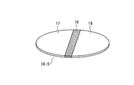
(第1の実施形態の変形例5)
これまでは、検出用バンプ接合部21と接触する領域(接触領域)のうち、接触領域の中心を含む領域に絶縁部が形成される例を説明したが、絶縁部は、接触領域の中心を含む領域に形成される必要はない。図13は、第1の実施形態の変形例5のパッド16−6の形状を示す図である。
(Modification 5 of the first embodiment)
So far, the example in which the insulating portion is formed in the region including the center of the contact region in the region (contact region) in contact with the detection
図13に示すように、本変形例の電子機器は、電極部17と電極部18とを絶縁する絶縁部19が、接触領域の中心を含まない領域に形成されている。このような構成では、電極部17の面積が電極部18の面積より小さいため、電極部17で破断が生じやすくなる。これにより、電子部品11と検出用バンプ接合部21と回路基板14とが機械的に接続された状態であっても、破断を検出することができる。
As shown in FIG. 13, in the electronic device of this modification, an insulating
なお、絶縁部が形成されたパッド(パッド16、16−2、16−3、16−4、16−5)の形状は一例であり、複数の電極(例えば電極部17、18)、および、複数の電極を互いに絶縁する絶縁部が形成されるものであればあらゆる形状を適用できる。このような形状により、き裂が中央に達しなくても電気的に破断し、検出用バンプ接合部21の破断をより早期に検出可能となる。すなわち、第1の実施形態にかかる電子機器では、回路基板と電子部品との接合部の破断を精度よく事前に検出することができる。
The shape of the pads (
また、これまでは絶縁部を形成したパッドを回路基板14上に形成する例を説明した。絶縁部を形成するパッドを電子部品11上に形成してもよいし、絶縁部を形成するパッドを回路基板14および電子部品11の両方に形成してもよい。
Further, the example in which the pad on which the insulating portion is formed is formed on the
(第2の実施形態)
次に、第2の実施形態について説明する。図14は、第2の実施形態の電子機器における電子部品の検出用バンプ接合部周辺の断面図である。図15は、検出用バンプ接合部のパッドの形状を示す図である。
(Second Embodiment)
Next, a second embodiment will be described. FIG. 14 is a cross-sectional view of the periphery of a bump bonding portion for detection of an electronic component in the electronic apparatus according to the second embodiment. FIG. 15 is a diagram illustrating the shape of the pad of the detection bump bonding portion.
本実施形態は、図1に示す第1の実施形態の電子機器と同様の構造を具備している。第2の実施形態では、第1の実施形態と異なる箇所について説明する。 This embodiment has the same structure as the electronic device of the first embodiment shown in FIG. In the second embodiment, parts different from the first embodiment will be described.
図14と図15に示すように、第2の実施形態の電子機器は、第1の実施形態の電子機器と比較して、検出用バンプ接合部21と接続している回路基板14上のパッド216の形状が異なる。本実施形態では、図14と図15に示すように、パッド216は、円形状に形成された電極部27と、電極部27上の中央部に形成された、電極部27より直径が小さい円形状の絶縁部219とから形成されている。なお、絶縁部219は、電極部27の中央部(中心を含む領域)に形成される必要はなく、破断せずに残ると予想される部分に形成されていればよい。
As shown in FIGS. 14 and 15, the electronic device according to the second embodiment has a pad on the
本実施形態では、パッド15と電極部27が、回路基板14に形成された配線222に電気的に接続され、電子部品側パッド12、13が、電子部品11に形成された配線28に電気的に接続されている。本実施形態では、パッド15、バンプ接合部20、電子部品側パッド12、配線28、電子部品側パッド13、検出用バンプ接合部21、電極部27、配線222の順に導電する接続経路に、検出部42が接続される。
In the present embodiment, the
本実施形態では、回路基板14と電子部品11の両方で電気特性値を測定するための配線を形成することが可能であれば、電極部27が複数の電極部から形成されている必要がないため、従来の部品の形状を変更することなく適用でき、実装が容易である。また、電子部品側パッド13近傍で、検出用バンプ接合部21が破断した場合にも、検出部42により破断を検出することができるため、より精度が向上する。
In the present embodiment, the
(第2の実施形態の変形例1)
次に、第2の実施形態の変形例1について説明する。図16は、第2の実施形態の変形例1の電子機器における検出用バンプ接合部周辺の断面図である。図17は、第2の実施形態の変形例1の電子部品側パッドの形状を示す図である。なお、この変形例の説明では、第2の実施形態の電子機器と異なる箇所について説明する。
(Modification 1 of 2nd Embodiment)
Next, Modification 1 of the second embodiment will be described. FIG. 16 is a cross-sectional view of the periphery of the detection bump bonding portion in the electronic apparatus according to Modification 1 of the second embodiment. FIG. 17 is a diagram illustrating the shape of the electronic component-side pad according to the first modification of the second embodiment. In the description of this modification, parts different from the electronic device of the second embodiment will be described.
図16および図17に示すように、本変形例では、第2の実施形態の電子機器と比較して、検出用バンプ接合部21の電子部品側パッド213は、電極部29と、電極部29上の中央部に形成された、電極部29の直径より小さい円形状の絶縁部30とから形成されている。
As shown in FIGS. 16 and 17, in this modification, the electronic
本変形例では、回路基板14上および電子部品11上の両方のパッドに絶縁部が形成されていることになる。したがって、電子部品側パッド213近傍と回路基板14上のパッド216近傍のいずれでき裂が発生した場合でも、検出用バンプ接合部21の破断検出を早める効果があり、バンプ接合部20の破断を事前に予測することができる。
In the present modification, insulating portions are formed on both pads on the
以上説明したとおり、第1から第2の実施形態によれば、回路基板と電子部品との接合部の破断を精度よく事前に検出することができる。 As described above, according to the first and second embodiments, it is possible to accurately detect in advance the breakage of the joint portion between the circuit board and the electronic component.
なお、本実施形態は、上記実施形態そのままに限定されるものではなく、実施段階ではその要旨を逸脱しない範囲で構成要素を変形して具体化することができる。また、上記実施形態に開示されている複数の構成要素の適宜な組み合わせにより、種々の発明を形成することができる。例えば、実施形態に示される全構成要素からいくつかの構成要素を削除してもよい。さらに、異なる実施形態にわたる構成要素を適宜組み合わせても良い。 Note that the present embodiment is not limited to the above-described embodiment as it is, and can be embodied by modifying the components without departing from the scope of the invention in the implementation stage. Moreover, various inventions can be formed by appropriately combining a plurality of constituent elements disclosed in the embodiment. For example, some components may be deleted from all the components shown in the embodiment. Furthermore, the constituent elements over different embodiments may be appropriately combined.
11 電子部品
12、13 電子部品側パッド
14 回路基板
15、16 パッド
17、18 電極部
19 絶縁部
20 バンプ接合部
21 検出用バンプ接合部
22 配線
41 チップ
42 検出部
DESCRIPTION OF
Claims (9)
回路基板と、
電子部品と、
前記回路基板上に形成された第1パッドと、
前記電子部品上に形成された第2パッドと、
前記第1パッドと前記第2パッドとを接合する接合部と、
前記第1パッドおよび前記第2のパッドの少なくとも一方と、前記接合部とを含む接続経路の電気特性に基づいて、前記接合部が前記電子機器の使用に伴い破断したことを検出する検出部と、を備え、
前記第1パッドおよび前記第2パッドの少なくとも一方は、前記接合部との接触領域の一部に絶縁部が形成され、
前記第1パッドと前記接合部との接触領域および前記第2パッドと前記接合部との接触領域の両方に前記絶縁部が形成されている場合は、2つの接触領域のうち一方の面積は他方の面積より小さく、
前記第1パッドと前記接合部との接触領域および前記第2パッドと前記接合部との接触領域の一方に前記絶縁部が形成されている場合は、前記絶縁部が形成されている接触領域の面積は、前記絶縁部が形成されていない接触領域の面積より小さいこと、
を特徴とする電子機器。 Electronic equipment,
A circuit board;
Electronic components,
A first pad formed on the circuit board;
A second pad formed on the electronic component;
A bonding portion for bonding the first pad and the second pad;
A detection unit configured to detect that the joint portion is broken with use of the electronic device based on an electrical characteristic of a connection path including at least one of the first pad and the second pad and the joint portion; With
At least one of the first pad and the second pad has an insulating part formed in a part of a contact area with the joint part ,
When the insulating part is formed in both the contact region between the first pad and the joint and the contact region between the second pad and the joint, the area of one of the two contact regions is the other Smaller than the area of
When the insulating part is formed in one of the contact area between the first pad and the bonding part and the contact area between the second pad and the bonding part, the contact area where the insulating part is formed The area is smaller than the area of the contact region where the insulating part is not formed ,
Electronic equipment characterized by
前記検出部は、複数の前記電極のうち、少なくとも2つの電極を含む前記接続経路の電気特性に基づいて前記接合部の破断を検出すること、
を特徴とする請求項1に記載の電子機器。 At least one of the first pad and the second pad includes a plurality of electrodes in which an insulating part is formed in a part of the contact region and insulated from each other by the insulating part,
The detection unit detects breakage of the joint based on electrical characteristics of the connection path including at least two electrodes among the plurality of electrodes;
The electronic device according to claim 1.
を特徴とする請求項1に記載の電子機器。 At least one of the first pad and the second pad includes one electrode, and an insulating portion is formed in a part of a contact region of the electrode with the joint portion;
The electronic device according to claim 1.
を特徴とする請求項1〜3のいずれか1つに記載の電子機器。 At least one of the first pad and the second pad has the insulating portion formed in a region including a center of the contact region in the contact region,
The electronic device according to claim 1, wherein
を特徴とする請求項1〜4のいずれか1つに記載の電子機器。 The thermal expansion coefficient of the insulating portion is different from the thermal expansion coefficient of the joint portion;
The electronic device according to claim 1, wherein:
を特徴とする請求項1〜5のいずれか1つに記載の電子機器。 The joint is a solder bump;
The electronic device according to any one of claims 1 to 5 , wherein
複数の前記第1パッドのうち、前記電子部品の周縁部に対向する前記第1パッドの少なくとも一部は、前記接触領域の一部に絶縁部が形成されていること、
を特徴とする請求項1〜6のいずれか1つに記載の電子機器。 A plurality of the first pads are formed on the circuit board,
Among the plurality of first pads, at least a part of the first pad facing a peripheral part of the electronic component has an insulating part formed in a part of the contact region,
The electronic device according to any one of claims 1 to 6 .
複数の前記第2パッドのうち、前記電子部品の周縁部に形成された前記第2パッドの少なくとも一部は、前記接触領域の一部に絶縁部が形成されていること、
を特徴とする請求項1〜6のいずれか1つに記載の電子機器。 A plurality of the second pads are formed on the electronic component,
Among the plurality of second pads, at least a part of the second pad formed on the peripheral part of the electronic component has an insulating part formed in a part of the contact region,
The electronic device according to any one of claims 1 to 6 .
を特徴とする請求項1〜8のいずれか1つに記載の電子機器。 The insulating part is covered with a solder resist;
The electronic device according to any one of claims 1 to 8 , wherein
Priority Applications (2)
| Application Number | Priority Date | Filing Date | Title |
|---|---|---|---|
| JP2010191766A JP5259659B2 (en) | 2010-08-30 | 2010-08-30 | Electronics |
| US13/041,820 US8581616B2 (en) | 2010-08-30 | 2011-03-07 | Electronic device |
Applications Claiming Priority (1)
| Application Number | Priority Date | Filing Date | Title |
|---|---|---|---|
| JP2010191766A JP5259659B2 (en) | 2010-08-30 | 2010-08-30 | Electronics |
Related Child Applications (1)
| Application Number | Title | Priority Date | Filing Date |
|---|---|---|---|
| JP2013031017A Division JP5450852B2 (en) | 2013-02-20 | 2013-02-20 | Electronics |
Publications (2)
| Publication Number | Publication Date |
|---|---|
| JP2012049418A JP2012049418A (en) | 2012-03-08 |
| JP5259659B2 true JP5259659B2 (en) | 2013-08-07 |
Family
ID=45696311
Family Applications (1)
| Application Number | Title | Priority Date | Filing Date |
|---|---|---|---|
| JP2010191766A Expired - Fee Related JP5259659B2 (en) | 2010-08-30 | 2010-08-30 | Electronics |
Country Status (2)
| Country | Link |
|---|---|
| US (1) | US8581616B2 (en) |
| JP (1) | JP5259659B2 (en) |
Families Citing this family (7)
| Publication number | Priority date | Publication date | Assignee | Title |
|---|---|---|---|---|
| JP5894515B2 (en) * | 2012-09-28 | 2016-03-30 | 株式会社東芝 | Semiconductor device, life estimation device, life estimation method |
| JP6076208B2 (en) * | 2013-06-21 | 2017-02-08 | 株式会社日本マイクロニクス | Wiring board inspection apparatus and wiring board inspection method |
| JP6235415B2 (en) * | 2014-06-10 | 2017-11-22 | アルプス電気株式会社 | Humidity detector |
| JP6532726B2 (en) * | 2015-03-27 | 2019-06-19 | 株式会社東芝 | Electronic device, abnormality determination method, and program |
| US20190011497A1 (en) * | 2017-07-09 | 2019-01-10 | Texas Instruments Incorporated | Test Fixture with Sintered Connections Between Mother Board and Daughter Board |
| EP3716747B1 (en) * | 2017-11-22 | 2023-03-29 | Fuji Corporation | Electronic component mounting machine and electronic component mounting method |
| DE102021209892A1 (en) * | 2021-09-08 | 2023-03-09 | Robert Bosch Gesellschaft mit beschränkter Haftung | Electronic control unit and method for monitoring solder joints of an electronic control unit |
Family Cites Families (10)
| Publication number | Priority date | Publication date | Assignee | Title |
|---|---|---|---|---|
| JPH03265197A (en) | 1990-03-14 | 1991-11-26 | Kanegafuchi Chem Ind Co Ltd | Radio wave absorber |
| JPH05347473A (en) | 1992-06-15 | 1993-12-27 | Toshiba Corp | Wiring board |
| US5786701A (en) * | 1993-07-02 | 1998-07-28 | Mitel Semiconductor Limited | Bare die testing |
| JP2825085B2 (en) * | 1996-08-29 | 1998-11-18 | 日本電気株式会社 | Semiconductor device mounting structure, mounting board, and mounting state inspection method |
| JP3265197B2 (en) | 1996-09-12 | 2002-03-11 | 株式会社東芝 | Semiconductor device |
| US6081429A (en) * | 1999-01-20 | 2000-06-27 | Micron Technology, Inc. | Test interposer for use with ball grid array packages assemblies and ball grid array packages including same and methods |
| JP2003121492A (en) * | 2001-10-15 | 2003-04-23 | Matsushita Electric Ind Co Ltd | Contact structure with spherical bump |
| JP4172238B2 (en) * | 2002-09-19 | 2008-10-29 | 日本電気株式会社 | Electronic component mounting structure |
| JP2009257863A (en) | 2008-04-15 | 2009-11-05 | Ricoh Elemex Corp | Electronic circuit board |
| JP2010093231A (en) | 2008-09-11 | 2010-04-22 | Yokogawa Electric Corp | Semiconductor mounting structure |
-
2010
- 2010-08-30 JP JP2010191766A patent/JP5259659B2/en not_active Expired - Fee Related
-
2011
- 2011-03-07 US US13/041,820 patent/US8581616B2/en not_active Expired - Fee Related
Also Published As
| Publication number | Publication date |
|---|---|
| US20120049885A1 (en) | 2012-03-01 |
| US8581616B2 (en) | 2013-11-12 |
| JP2012049418A (en) | 2012-03-08 |
Similar Documents
| Publication | Publication Date | Title |
|---|---|---|
| JP5259659B2 (en) | Electronics | |
| JP4901602B2 (en) | Printed circuit board manufacturing method and printed circuit board | |
| CN108225963B (en) | PCB design method based on BGA solder joint reliability test | |
| JP5032213B2 (en) | Electronics | |
| US9277657B2 (en) | Wiring board | |
| JP6466128B2 (en) | Probe card | |
| CN103219322A (en) | Three dimensional integrated circuit having a resistance measurment structure and method of use | |
| CN101894819B (en) | Substrate structure | |
| CN101411252A (en) | Circuit board, method for testing circuit board, and method for manufacturing circuit board | |
| JP2016025159A (en) | Wiring board structure and manufacturing method of wiring board structure | |
| JP6236841B2 (en) | Multilayer wiring board and manufacturing method thereof | |
| JP5450852B2 (en) | Electronics | |
| WO2013094678A1 (en) | Electronic device, power source control system, and service life measurement unit | |
| JP5355149B2 (en) | Electronic device and method of detecting connection failure of electronic component using electronic device | |
| JP2009239027A (en) | Semiconductor device with defect detecting function | |
| JP2010278212A (en) | Electronic component package and method for detecting abnormality of electronic component package | |
| JP5370250B2 (en) | Manufacturing method of semiconductor device | |
| CN103715167A (en) | Semiconductor device, apparatus of estimating lifetime, method of estimating lifetime | |
| KR102689407B1 (en) | A space transformer for a probe card having improved heat dissipation property | |
| KR102469361B1 (en) | Installation structure of thermal fuse | |
| JP2021185589A (en) | Wiring board | |
| CN203038917U (en) | CPI test structure | |
| JP2014096506A (en) | Semiconductor device and method for manufacturing semiconductor device | |
| JP5540854B2 (en) | Semiconductor substrate | |
| JP2011009322A (en) | Pattern leading out structure and semiconductor device |
Legal Events
| Date | Code | Title | Description |
|---|---|---|---|
| A977 | Report on retrieval |
Free format text: JAPANESE INTERMEDIATE CODE: A971007 Effective date: 20120817 |
|
| A131 | Notification of reasons for refusal |
Free format text: JAPANESE INTERMEDIATE CODE: A131 Effective date: 20120821 |
|
| A521 | Written amendment |
Free format text: JAPANESE INTERMEDIATE CODE: A523 Effective date: 20121016 |
|
| A02 | Decision of refusal |
Free format text: JAPANESE INTERMEDIATE CODE: A02 Effective date: 20121211 |
|
| A521 | Written amendment |
Free format text: JAPANESE INTERMEDIATE CODE: A523 Effective date: 20130220 |
|
| A911 | Transfer to examiner for re-examination before appeal (zenchi) |
Free format text: JAPANESE INTERMEDIATE CODE: A911 Effective date: 20130227 |
|
| TRDD | Decision of grant or rejection written | ||
| A01 | Written decision to grant a patent or to grant a registration (utility model) |
Free format text: JAPANESE INTERMEDIATE CODE: A01 Effective date: 20130402 |
|
| A61 | First payment of annual fees (during grant procedure) |
Free format text: JAPANESE INTERMEDIATE CODE: A61 Effective date: 20130424 |
|
| FPAY | Renewal fee payment (event date is renewal date of database) |
Free format text: PAYMENT UNTIL: 20160502 Year of fee payment: 3 |
|
| R151 | Written notification of patent or utility model registration |
Ref document number: 5259659 Country of ref document: JP Free format text: JAPANESE INTERMEDIATE CODE: R151 |
|
| S111 | Request for change of ownership or part of ownership |
Free format text: JAPANESE INTERMEDIATE CODE: R313111 |
|
| R350 | Written notification of registration of transfer |
Free format text: JAPANESE INTERMEDIATE CODE: R350 |
|
| LAPS | Cancellation because of no payment of annual fees |