JP5258142B2 - Aluminum pad power bus and signal routing technology for integrated circuit devices using copper technology interconnect structures - Google Patents
Aluminum pad power bus and signal routing technology for integrated circuit devices using copper technology interconnect structures Download PDFInfo
- Publication number
- JP5258142B2 JP5258142B2 JP2004114863A JP2004114863A JP5258142B2 JP 5258142 B2 JP5258142 B2 JP 5258142B2 JP 2004114863 A JP2004114863 A JP 2004114863A JP 2004114863 A JP2004114863 A JP 2004114863A JP 5258142 B2 JP5258142 B2 JP 5258142B2
- Authority
- JP
- Japan
- Prior art keywords
- interconnect
- integrated circuit
- power bus
- circuit device
- layer
- Prior art date
- Legal status (The legal status is an assumption and is not a legal conclusion. Google has not performed a legal analysis and makes no representation as to the accuracy of the status listed.)
- Expired - Fee Related
Links
Images


Classifications
-
- H—ELECTRICITY
- H01—ELECTRIC ELEMENTS
- H01L—SEMICONDUCTOR DEVICES NOT COVERED BY CLASS H10
- H01L21/00—Processes or apparatus adapted for the manufacture or treatment of semiconductor or solid state devices or of parts thereof
- H01L21/70—Manufacture or treatment of devices consisting of a plurality of solid state components formed in or on a common substrate or of parts thereof; Manufacture of integrated circuit devices or of parts thereof
- H01L21/71—Manufacture of specific parts of devices defined in group H01L21/70
- H01L21/768—Applying interconnections to be used for carrying current between separate components within a device comprising conductors and dielectrics
-
- H—ELECTRICITY
- H01—ELECTRIC ELEMENTS
- H01L—SEMICONDUCTOR DEVICES NOT COVERED BY CLASS H10
- H01L23/00—Details of semiconductor or other solid state devices
- H01L23/52—Arrangements for conducting electric current within the device in operation from one component to another, i.e. interconnections, e.g. wires, lead frames
- H01L23/522—Arrangements for conducting electric current within the device in operation from one component to another, i.e. interconnections, e.g. wires, lead frames including external interconnections consisting of a multilayer structure of conductive and insulating layers inseparably formed on the semiconductor body
- H01L23/528—Geometry or layout of the interconnection structure
- H01L23/5286—Arrangements of power or ground buses
-
- H—ELECTRICITY
- H01—ELECTRIC ELEMENTS
- H01L—SEMICONDUCTOR DEVICES NOT COVERED BY CLASS H10
- H01L21/00—Processes or apparatus adapted for the manufacture or treatment of semiconductor or solid state devices or of parts thereof
- H01L21/70—Manufacture or treatment of devices consisting of a plurality of solid state components formed in or on a common substrate or of parts thereof; Manufacture of integrated circuit devices or of parts thereof
- H01L21/71—Manufacture of specific parts of devices defined in group H01L21/70
- H01L21/768—Applying interconnections to be used for carrying current between separate components within a device comprising conductors and dielectrics
- H01L21/76838—Applying interconnections to be used for carrying current between separate components within a device comprising conductors and dielectrics characterised by the formation and the after-treatment of the conductors
- H01L21/76885—By forming conductive members before deposition of protective insulating material, e.g. pillars, studs
-
- H—ELECTRICITY
- H01—ELECTRIC ELEMENTS
- H01L—SEMICONDUCTOR DEVICES NOT COVERED BY CLASS H10
- H01L23/00—Details of semiconductor or other solid state devices
- H01L23/52—Arrangements for conducting electric current within the device in operation from one component to another, i.e. interconnections, e.g. wires, lead frames
- H01L23/522—Arrangements for conducting electric current within the device in operation from one component to another, i.e. interconnections, e.g. wires, lead frames including external interconnections consisting of a multilayer structure of conductive and insulating layers inseparably formed on the semiconductor body
- H01L23/528—Geometry or layout of the interconnection structure
- H01L23/5283—Cross-sectional geometry
-
- H—ELECTRICITY
- H01—ELECTRIC ELEMENTS
- H01L—SEMICONDUCTOR DEVICES NOT COVERED BY CLASS H10
- H01L2224/00—Indexing scheme for arrangements for connecting or disconnecting semiconductor or solid-state bodies and methods related thereto as covered by H01L24/00
- H01L2224/01—Means for bonding being attached to, or being formed on, the surface to be connected, e.g. chip-to-package, die-attach, "first-level" interconnects; Manufacturing methods related thereto
- H01L2224/42—Wire connectors; Manufacturing methods related thereto
- H01L2224/44—Structure, shape, material or disposition of the wire connectors prior to the connecting process
- H01L2224/45—Structure, shape, material or disposition of the wire connectors prior to the connecting process of an individual wire connector
- H01L2224/45001—Core members of the connector
- H01L2224/45099—Material
- H01L2224/451—Material with a principal constituent of the material being a metal or a metalloid, e.g. boron (B), silicon (Si), germanium (Ge), arsenic (As), antimony (Sb), tellurium (Te) and polonium (Po), and alloys thereof
- H01L2224/45138—Material with a principal constituent of the material being a metal or a metalloid, e.g. boron (B), silicon (Si), germanium (Ge), arsenic (As), antimony (Sb), tellurium (Te) and polonium (Po), and alloys thereof the principal constituent melting at a temperature of greater than or equal to 950°C and less than 1550°C
- H01L2224/45144—Gold (Au) as principal constituent
-
- H—ELECTRICITY
- H01—ELECTRIC ELEMENTS
- H01L—SEMICONDUCTOR DEVICES NOT COVERED BY CLASS H10
- H01L2224/00—Indexing scheme for arrangements for connecting or disconnecting semiconductor or solid-state bodies and methods related thereto as covered by H01L24/00
- H01L2224/01—Means for bonding being attached to, or being formed on, the surface to be connected, e.g. chip-to-package, die-attach, "first-level" interconnects; Manufacturing methods related thereto
- H01L2224/42—Wire connectors; Manufacturing methods related thereto
- H01L2224/47—Structure, shape, material or disposition of the wire connectors after the connecting process
- H01L2224/48—Structure, shape, material or disposition of the wire connectors after the connecting process of an individual wire connector
- H01L2224/4805—Shape
- H01L2224/4809—Loop shape
- H01L2224/48091—Arched
-
- H—ELECTRICITY
- H01—ELECTRIC ELEMENTS
- H01L—SEMICONDUCTOR DEVICES NOT COVERED BY CLASS H10
- H01L2224/00—Indexing scheme for arrangements for connecting or disconnecting semiconductor or solid-state bodies and methods related thereto as covered by H01L24/00
- H01L2224/01—Means for bonding being attached to, or being formed on, the surface to be connected, e.g. chip-to-package, die-attach, "first-level" interconnects; Manufacturing methods related thereto
- H01L2224/42—Wire connectors; Manufacturing methods related thereto
- H01L2224/47—Structure, shape, material or disposition of the wire connectors after the connecting process
- H01L2224/49—Structure, shape, material or disposition of the wire connectors after the connecting process of a plurality of wire connectors
- H01L2224/491—Disposition
- H01L2224/4912—Layout
- H01L2224/49171—Fan-out arrangements
-
- H—ELECTRICITY
- H01—ELECTRIC ELEMENTS
- H01L—SEMICONDUCTOR DEVICES NOT COVERED BY CLASS H10
- H01L23/00—Details of semiconductor or other solid state devices
- H01L23/52—Arrangements for conducting electric current within the device in operation from one component to another, i.e. interconnections, e.g. wires, lead frames
- H01L23/522—Arrangements for conducting electric current within the device in operation from one component to another, i.e. interconnections, e.g. wires, lead frames including external interconnections consisting of a multilayer structure of conductive and insulating layers inseparably formed on the semiconductor body
- H01L23/532—Arrangements for conducting electric current within the device in operation from one component to another, i.e. interconnections, e.g. wires, lead frames including external interconnections consisting of a multilayer structure of conductive and insulating layers inseparably formed on the semiconductor body characterised by the materials
- H01L23/53204—Conductive materials
- H01L23/53209—Conductive materials based on metals, e.g. alloys, metal silicides
- H01L23/53214—Conductive materials based on metals, e.g. alloys, metal silicides the principal metal being aluminium
-
- H—ELECTRICITY
- H01—ELECTRIC ELEMENTS
- H01L—SEMICONDUCTOR DEVICES NOT COVERED BY CLASS H10
- H01L23/00—Details of semiconductor or other solid state devices
- H01L23/52—Arrangements for conducting electric current within the device in operation from one component to another, i.e. interconnections, e.g. wires, lead frames
- H01L23/522—Arrangements for conducting electric current within the device in operation from one component to another, i.e. interconnections, e.g. wires, lead frames including external interconnections consisting of a multilayer structure of conductive and insulating layers inseparably formed on the semiconductor body
- H01L23/532—Arrangements for conducting electric current within the device in operation from one component to another, i.e. interconnections, e.g. wires, lead frames including external interconnections consisting of a multilayer structure of conductive and insulating layers inseparably formed on the semiconductor body characterised by the materials
- H01L23/53204—Conductive materials
- H01L23/53209—Conductive materials based on metals, e.g. alloys, metal silicides
- H01L23/53228—Conductive materials based on metals, e.g. alloys, metal silicides the principal metal being copper
Description
本願は、銅技術相互接続構造を使用する集積回路デバイス用のアルミニウム・パッド電力バス及び信号ルーティング技術に関する。
本特許出願は、2003年4月10日に出願の「銅技術におけるアルミニウム・パッド電力バス(Aluminum Pad Power Bus)」という名称の米国仮特許出願第60/462,504号の特典を請求する。
This application relates to aluminum pad power bus and signal routing technology for integrated circuit devices using copper technology interconnect structures.
This patent application claims the benefit of US Provisional Patent Application No. 60 / 462,504, filed April 10, 2003, entitled “Aluminum Pad Power Bus”.
集積回路(またはチップ)は、通常シリコン基板、および基板内のドープ領域から形成されるトランジスタなどの半導体デバイスを含む。半導体基板の上の平行状の層内に形成された相互接続構造が、デバイス間を電気的に接続して、電気回路を形成する。典型的な集積回路内のデバイスを相互接続するためには、通常いくつかの(例えば6〜9層の)相互接続層(それぞれ「M」またはメタライゼーション層と呼ばれる)が必要である。最上部の相互接続層は複数のパッドを備え、このパッドはパッケージ構造のピンまたはリードなど外部チップの外部接点にこの集積回路デバイスを相互接続するための導電性エレメント(例えば、ボンド線またははんだボール)用の接続点として働く。 Integrated circuits (or chips) typically include semiconductor devices such as transistors formed from a silicon substrate and doped regions within the substrate. Interconnect structures formed in parallel layers on the semiconductor substrate electrically connect the devices to form an electrical circuit. In order to interconnect devices in a typical integrated circuit, usually several (e.g. 6-9) interconnect layers (respectively referred to as "M" or metallization layers) are required. The top interconnect layer includes a plurality of pads that are conductive elements (eg, bond lines or solder balls) for interconnecting the integrated circuit device to external contacts of an external chip, such as package structure pins or leads. ) Serve as a connection point.
通常の相互接続システムは、複数の実質上垂直な導電性バイアまたはプラグと、実質上水平な導電性相互接続層とを備え、2つの縦に隣接する相互接続層の間には誘電体層が配設されている。上側レベルの導電性バイアは、2つの縦に隣接する相互接続層を相互接続する。第1または最下部のレベル内の導電性バイアは、下層の半導体デバイス領域を上層の相互接続層に相互接続する。通常の金属堆積、フォトリソグラフィ・マスキング、フォトリソグラフィ・パターニング、およびフォトリソグラフィ・エッチング技術を用いることによって、相互接続構造は形成される。 A typical interconnect system includes a plurality of substantially vertical conductive vias or plugs and a substantially horizontal conductive interconnect layer, with a dielectric layer between two vertically adjacent interconnect layers. It is arranged. An upper level conductive via interconnects two vertically adjacent interconnect layers. Conductive vias in the first or bottom level interconnect the lower semiconductor device region to the upper interconnect layer. The interconnect structure is formed by using conventional metal deposition, photolithography masking, photolithography patterning, and photolithography etching techniques.
集積回路デバイスおよび相互接続構造が小型化し、デバイスがより高い周波数アナログ信号およびより速いデータ転送速度のデジタル信号を伝達するようになるにつれて、相互接続構造が、信号伝播時間に遅延を加える恐れがあるので不利である。さらに、デバイスおよび付加された機能がますます複雑になるにつれて、より多くの相互接続構造またはレベルが必要となるかもしれない。しかし通常の相互接続メタライゼーション材料、例えばアルミニウムは信号速度を極度に制限する。さらに、特に回路デバイスおよび相互接続構造の数が増加するにつれて、アルミニウム相互接続構造とデバイス・シリコン領域の間の接点抵抗が全回路抵抗の主要な原因となる。最後に、相互接続の線幅が縮小するにつれて、開口またはウィンドウ内に導電材料を堆積させて、高いアスペクト比(すなわち開口深さと開口直径の比率)の導電性バイアを形成することがますます難しくなってきている。 As integrated circuit devices and interconnect structures become smaller and devices carry higher frequency analog signals and higher data rate digital signals, the interconnect structures can add delay to signal propagation time. So it is disadvantageous. In addition, as devices and added functionality become increasingly complex, more interconnect structures or levels may be required. However, conventional interconnect metallization materials, such as aluminum, severely limit signal speed. In addition, contact resistance between the aluminum interconnect structure and the device silicon region is a major source of total circuit resistance, especially as the number of circuit devices and interconnect structures increases. Finally, as interconnect linewidths shrink, it becomes increasingly difficult to deposit conductive materials within openings or windows to form high aspect ratio (ie, ratio of opening depth to opening diameter) conductive vias. It has become to.
アルミニウム相互接続構造には周知の欠点があることから、銅が最適な相互接続材料となりつつある。銅はアルミニウムより良好な導電体であり(アルミニウムの3.1μΩ・cmと比較して1.7μΩ・cmの抵抗を持つ)、エレクトロマイグレーション(アルミニウム相互接続を介する電流の流れによって生じる電界および温度勾配により、アルミニウム相互接続構造が薄くなり、最終的には分離する恐れがある現象)の影響を受けにくく、より低い温度で堆積させることができ(そのため、あらかじめ形成されたドーパント・プロファイルに対する有害な影響が回避される)、高いアスペクト比の適用分野において使用するのに適する。 Because of the well-known drawbacks of aluminum interconnect structures, copper is becoming the optimal interconnect material. Copper is a better conductor than aluminum (having a resistance of 1.7 μΩ · cm compared to 3.1 μΩ · cm for aluminum) and electromigration (electric field and temperature gradients caused by current flow through the aluminum interconnect) Makes the aluminum interconnect structure thinner and less susceptible to segregation, and can be deposited at lower temperatures (and therefore detrimental effects on preformed dopant profiles) Is suitable for use in high aspect ratio applications.
ダマシン・プロセスは、集積回路デバイス用の銅相互接続構造を形成する一技術である。通常、銅ダマシン・プロセスは、導電性の垂直なバイア部分と相互接続層またはメタライゼーション層からなる導電性の水平な相互接続部分(金属ランナと呼ばれる)の両方を一体形成する。銅のダマシン構造を形成するためには、誘電体層内にホールまたはウィンドウを形成し、続いて金属ランナ用の上層のトレンチを形成する。後続の金属堆積工程で開口とトレンチの両方を充填して、実質上垂直な導電性バイアおよび実質上水平な導電性ランナを備える完成した金属層を形成する。最後の化学的機械研磨工程により、誘電体層の隣接した表面を基準にして、堆積された金属を平坦化する。 The damascene process is one technique for forming copper interconnect structures for integrated circuit devices. Typically, the copper damascene process integrally forms both conductive vertical via portions and conductive horizontal interconnect portions (called metal runners) consisting of interconnect layers or metallization layers. To form a copper damascene structure, holes or windows are formed in the dielectric layer, followed by an upper trench for the metal runner. Subsequent metal deposition steps fill both the openings and the trenches to form a finished metal layer with substantially vertical conductive vias and substantially horizontal conductive runners. A final chemical mechanical polishing step planarizes the deposited metal relative to the adjacent surface of the dielectric layer.
従来技術のデュアル・ダマシン・プロセスの例を、様々な製造段階における図1A〜1Cからなる断面図に示す。図1Aに示すように、下側のレベルの相互接続12上に、誘電体層10を堆積または形成する。誘電体層10上に形成されたフォトレジスト層16を、通常の技術に従ってパターン形成し、エッチングして、開口18をその中に形成する。異方性のエッチング・プロセスで、誘電体層10内に開口18を貫通してバイアホールまたはウィンドウ20をエッチングする。フォトレジスト層16を除去し、フォトレジスト層30で置き換え(図1Bを参照されたい)、次いでフォトレジスト層30をパターン形成しエッチングして、トレンチ・パターン32を形成する。異方性のエッチング・プロセスで、トレンチ34(図面の紙面に対して垂直に延びている)を形成し、同時に下側レベルの相互接続12の上部表面36まで開口18を延ばす。ホールまたはウィンドウ20は、上部表面36の上で止まり、下側レベルの相互接続12を(図1Bに示すように)露出させるように形成することができ、また下側レベルの相互接続12中に部分的に延びるようにオーバ・エッチングすることもできる。
An example of a prior art dual damascene process is shown in the cross-sectional view of FIGS. As shown in FIG. 1A, a
図1Cに示すように、ホール20およびトレンチ34は、銅などの適切な導電材料40で同時に充填される。標準的なプロセス技術によれば、最初に銅シード層を堆積させ、続いて銅電気めっきを行ってホール20およびトレンチ34を充填する。したがって、材料40は、導電性トレンチ42、および下側レベルの相互接続12に接触する導電性バイア44を形成する。さらに、材料40が銅を含む場合、銅の堆積に先立ち、タンタル層および/または窒化タンタル層(または他の高融点材料およびそれらの窒化物)などのバリア層をホール20およびトレンチ34内に堆積させる。この1つまたは複数のバリア層は、誘電体層10の周囲の材料中に銅が拡散することを防ぐ。最後に、堆積後、フィールド領域48から余分の金属40を除去するために、当技術分野で周知の化学的機械研磨法(CMP)などの技術を使用して、誘電体層10の表面を平坦化する。
As shown in FIG. 1C,
集積回路デバイス用の従来技術のデュアル・ダマシン構造の第2の例を図2A〜2Cに示す。図2Aに示すように、下側レベルの相互接続58上には、第1のエッチング・ストップ層60、第1の誘電体層62、第2のエッチング・ストップ層64、第2の誘電体層66、およびエッチング・マスク68を含む複数の材料層が形成される。エッチング・マスク68をパターン形成し、エッチングして、開口70をその中に形成する。エッチング・マスク・パターンを使用して、異方性の第1のエッチング・プロセスで、第2の誘電体層66内に、第2のエッチング・ストップ層64を貫通して第1のエッチング・ストップ層60まで下方へ延びるバイア開口72を形成する。エッチング剤がエッチング・ストップ層60に達すると、エッチング・プロセスは終了する。エッチング・マスク68を除去し、エッチング・マスク78(図2Bを参照されたい)を第2の誘電体層66上に置き、マスクして、開口70より横方向に広い開口79を形成する。第2の異方性のエッチング・プロセスで、第2の誘電体層66内にトレンチ80をエッチングする。同時に、エッチング・ストップ層60を貫通してエッチングすることによって、バイア開口72は下方へ延びて、下層の下側レベルの相互接続58と接触する。この技術によれば、第1のエッチング剤は、第2のエッチング剤よりエッチング・ストップ層60に対する選択性が高い。マスク78を除去し、トレンチ80およびバイア開口72を、適切な導電性金属で同時に充填し(図2Cを参照されたい)、導電性ランナ88、および下側レベルの相互接続58と接触する導電性バイア90を形成すると、ダマシン・プロセスが完了する。余分な導電材料を、当技術分野では周知のCMPなどの技術を使用して、第2の誘電体層66のフィールド領域面92から除去する。
A second example of a prior art dual damascene structure for an integrated circuit device is shown in FIGS. As shown in FIG. 2A, on the
相互接続構造は、半導体素子の間で信号を伝える他に、アルミニウム製にせよ、または銅製にせよ、電力バス構造を介して様々なデバイス要素に電力を供給するために必要である。ほとんどの集積回路では、電力バスは、垂直な導電性バイアおよび水平な相互接続層を含めて追加の相互接続層として形成される。通常、電力バスは、上側レベルの相互接続構造を形成する。追加の電力バス相互接続層は、マスク工程、マスク層、およびプロセス工程の数を増やし、結局は製造費の増加の原因となるので不利である。さらに、これらの追加のプロセス工程は、処理中に欠陥を生じさせる可能性があるので、デバイスの歩留りを低下させる恐れがある。 In addition to transmitting signals between the semiconductor elements, the interconnect structure is necessary to supply power to various device elements via the power bus structure, whether aluminum or copper. In most integrated circuits, the power bus is formed as an additional interconnect layer, including vertical conductive vias and horizontal interconnect layers. Typically, the power bus forms an upper level interconnect structure. The additional power bus interconnect layer is disadvantageous because it increases the number of mask steps, mask layers, and process steps, which ultimately increases manufacturing costs. In addition, these additional process steps can cause defects during processing, which can reduce device yield.
電力バスは、信号相互接続構造に比べて、比較的大きな電流を通すので、電力バス相互接続層は、信号相互接続層より一般に幅が広く、厚みがあり、ピッチが大きい。電力バスはまた、ノイズおよび寄生容量の発生源であり、このノイズおよび寄生容量は、すぐ近くのデバイスおよび相互接続構造の性能を破壊する恐れがある。これらの影響を抑えるために、電力バスを他のデバイス構造から分離することができるか、絶縁構造が貴重なデバイス領域を消費してしまう。 Since the power bus conducts a relatively large current compared to the signal interconnect structure, the power bus interconnect layer is generally wider, thicker and larger in pitch than the signal interconnect layer. The power bus is also a source of noise and parasitic capacitance, which can destroy the performance of nearby devices and interconnect structures. To suppress these effects, the power bus can be isolated from other device structures, or the insulating structure consumes valuable device area.
集積回路デバイスは、半導体基板層上に形成される多段相互接続メタライゼーション・システムを含む。このメタライゼーション・システムは、ボンド・パッド・レベル、およびボンド・パッド・レベルの下の1つまたは複数の相互接続レベルを含む。ボンド・パッド・レベルは、デバイスの外部に接続するようにそれぞれ構成された複数のコンタクト・パッドと、1つまたは複数のパッドから1つまたは複数の下のレベルの相互接続に電力を伝えるように構成された相互接続とを含む。
以下の詳細な説明を、以下の図と併せ読めば、本発明をより容易に理解することができ、その利点および使用法がより簡単に明らかになる。
The integrated circuit device includes a multi-stage interconnect metallization system formed on a semiconductor substrate layer. The metallization system includes a bond pad level and one or more interconnect levels below the bond pad level. The bond pad level transmits power from one or more pads to one or more lower level interconnects, each configured to connect to the outside of the device. Configured interconnects.
The invention will be more readily understood and its advantages and uses will become more readily apparent when the following detailed description is read in conjunction with the following figures.
一般の慣例に従って、様々な記載されたデバイス・フィーチャを一定の縮尺で描かずに、本発明に関連する特定のフィーチャを強調するように描く。参照符号は、本図および本文の全体を通して同じ要素を指す。 In accordance with common practice, the various described device features are not drawn to scale but are drawn to emphasize specific features relevant to the present invention. Reference numerals refer to the same elements throughout the figures and text.
本発明による特定の集積回路デバイス用のアルミニウム・パッド電力バスまたは信号ルーティング技術を詳細に説明する前に、本発明が主に要素および方法工程の新規かつ非自明な組合せにあることを注目されたい。したがって、この説明の利益を有する当業者には容易に明らかとなるであろう構造上の細部に関する説明が不明確にならないように、これらの要素および工程を、本発明に関係する特定の細部だけを示した図面内で共通の要素および工程によって表した。 Before describing in detail an aluminum pad power bus or signal routing technique for a specific integrated circuit device according to the present invention, it should be noted that the present invention is primarily a novel and non-obvious combination of elements and method steps. . Accordingly, to avoid obscuring the description of the structural details that would be readily apparent to one of ordinary skill in the art having the benefit of this description, these elements and steps have been described with reference to specific details related to the invention. Are represented by common elements and processes in the drawings.
製造後、この集積回路は、チップ取り付け領域と、この集積回路を外部構成要素に接続する複数の外部に配設されたパッケージ・リードとを備えるパッケージ構造に取り付ける。パッケージ・リードは、薄く壊れやすい相互接続構造に直接接続することはできないため、アルミニウム・パッド層またはボンド・パッド層と呼ばれるチップの最終または上部のメタライゼーション層は、ボンド・パッドとパッケージ・リードの内部配設されたコンタクトの間に接続された導電性リード線または導電性ワイヤ(通常、金またはその合金から形成される)を介してパッケージ・リードに接続するための複数のボンド・パッドまたはコンタクト・パッドを備える。 After manufacture, the integrated circuit is attached to a package structure comprising a chip attachment region and a plurality of externally disposed package leads that connect the integrated circuit to external components. Because package leads cannot be directly connected to thin and fragile interconnect structures, the final or top metallization layer of the chip, called the aluminum pad layer or bond pad layer, is the bond pad and package lead A plurality of bond pads or contacts for connecting to package leads via conductive leads or conductive wires (typically formed of gold or alloys thereof) connected between internally disposed contacts・ Equipped with a pad.
このボンド・パッドは、金属バリア層、通常は、窒化タンタル、タンタル、または窒化チタンを堆積させ、続いて集積回路の上部表面にアルミニウム層を堆積させることによって形成する。このアルミニウム層に、通常のマスキング、パターニング、およびエッチング工程を施して、アルミニウム・ボンド・パッドを画定する。一実施形態では、アルミニウム層上に反射防止コーティング層を配設して、フォトリソグラフィ・プロセス中のアルミニウム反射を低減させる。反射防止コーティング層の材料は、窒化チタン、または酸窒化シリコンを含む。このボンド・パッドは、下層の導電性バイアを介して、1つまたは複数の下層の相互接続構造または回路要素に接続される。前記のダマシン・プロセスなどによって銅から相互接続構造を形成するデバイスでは、金線が銅のボンド・パッドには十分に付着しないことが知られているので、ボンド・パッドは通常アルミニウムで形成される。 The bond pad is formed by depositing a metal barrier layer, typically tantalum nitride, tantalum, or titanium nitride, followed by depositing an aluminum layer on the top surface of the integrated circuit. This aluminum layer is subjected to conventional masking, patterning, and etching steps to define an aluminum bond pad. In one embodiment, an anti-reflective coating layer is disposed on the aluminum layer to reduce aluminum reflection during the photolithography process. The material of the antireflection coating layer includes titanium nitride or silicon oxynitride. The bond pad is connected to one or more underlying interconnect structures or circuit elements via underlying conductive vias. In devices that form interconnect structures from copper, such as by the damascene process, bond pads are typically formed of aluminum, as gold wires are known not to adhere well to copper bond pads. .
図3は、パッケージ・リード102を備えるデバイス・パッケージ100を示す。集積回路104はダイ接着領域106内に取り付けられる。ボンド・パッド110は、集積回路104の上部表面112上に形成され、金線114によってパッケージ・リード102に接続される。一般に、ボンド・パッド110は、それぞれ縦が40〜80ミクロン、横が50〜150ミクロンの範囲である。正方形のボンド・パッドが一般的であるが、矩形のボンド・パッドが使用されことも従来技術では周知である。
FIG. 3 shows a
フリップチップ・ボンディングまたはバンプ・ボンディングと呼ばれる他の周知のパッケージ構造では、図3のボンド線114の代わりに、ボンド・パッド110上に形成された堆積済みのはんだバンプ120を使用する。図4Aを参照されたい。図4Bのパッケージ122への接続は、集積回路104を裏返し、パッケージ122上の対応するパッケージ・リードに接続されている受けパッド124にバンプ120をはんだ付けすることによって実施される。図4Bの例では、パッケージ・リードは、当技術分野で周知のように、ボール・グリッド・アレイの形のボール126を備える。
Another known package structure called flip chip bonding or bump bonding uses deposited solder bumps 120 formed on
パッケージ・リード102を集積回路104に、ボンド線114によって接続するにせよはんだバンプ120によって接続するにせよ、ボンド・パッド110をその中に形成するメタライゼーション層は必要である。本発明の教示によれば、アルミニウム・パッド層は、ボンド・パッドまたはコンタクト・パッドと電力バスまたは信号ルーティング相互接続構造の両方を備え、それを介して集積回路デバイスの要素に電力を分配し、また集積回路内に信号を送る。アルミニウム・パッド層はボンド・パッド110を形成するために必ず必要なので、本発明によって、製造プロセスに追加のプロセス工程、マスク工程、またはメタライゼーション・レベルが追加されることはない。それとは逆に、1つのメタライゼーション・レベルを削除することができる。本発明は、ボンド・パッド用のアルミニウムの堆積に先立ち、銅相互接続構造の上に通常通りデュアル・パッシベーション・スタックを形成するので、銅技術(すなわち、ダマシン相互接続構造)での使用に特に適している。したがって、第1のデュアル・パッシベーション・スタックは、下層の上側レベルの相互接続構造とアルミニウム・パッド層内に形成される上層の電力バスの間の有効な絶縁誘電体を形成する。
Whether the package leads 102 are connected to the
図5は、6段の金属相互接続構造のうち上部のメタライゼーション・レベル5および6だけを示す、集積回路デバイス用の通常の従来技術の相互接続メタライゼーション構造の断面図を示す。この例では、相互接続構造は、銅のデュアル・ダマシン相互接続構造を備える。本発明の教示は、6段または6つの相互接続構造以外の集積回路デバイスにも適用できることが当業者には理解されよう。 FIG. 5 shows a cross-sectional view of a conventional prior art interconnect metallization structure for an integrated circuit device showing only the upper metallization levels 5 and 6 of the six-stage metal interconnect structure. In this example, the interconnect structure comprises a copper dual damascene interconnect structure. Those skilled in the art will appreciate that the teachings of the present invention can be applied to integrated circuit devices other than six-stage or six-interconnect structures.
デュアル・ダマシン・プロセスによれば、誘電体層135、136内にそれぞれ前もって形成されたバイア開口およびトレンチ内に、導電性バイア130およびレベル5の導電性ランナ132、134を同時に形成する。導電性バイア130およびレベル5の導電性ランナ132、134は、エッチング・ストップ層137によって分離することができ、このエッチング・ストップ層137により、通常のデュアル・ダマシン処理に従ってバイア開口およびトレンチを別々に形成することが容易になる。しかし、エッチング・ストップ層137はデュアル・ダマシン要素が機能するには必要ではない。導電性バイア130は、図5には示さない下層の相互接続構造または回路要素に接続される。誘電体バリア層140(典型的な材料は、窒化シリコン、炭化シリコン、またはその組合せを含む)が、誘電体層136およびレベル5の導電性ランナ132、134の露出された上部表面の上にある。誘電体バリア層140は、次段の導電性バイアを製作するためのエッチング・ストップとして機能し、導電性ランナ132、134から誘電体層136中への銅の表面拡散を阻止するための拡散バリアとして働く。追加のバリア層141が、誘電材料中への横方向の銅拡散を防ぐために、様々な銅フィーチャを取り囲む。
According to the dual damascene process, conductive via 130 and level 5
誘電体層144内に形成されるレベル6の導電性バイア142は、下のレベル5の導電性ランナ132、134と電気的に接触している。誘電体バリア層145は、誘電体バリア層140と同じ目的を果たし、誘電体層144の上にある。誘電体層144の上の酸化物層148内には、電力バス146が形成される。前記のデュアル・ダマシン・プロセスに従って、前もって形成されたバイア開口およびトレンチ内に、導電性バイア142および電力バス146が同時に形成される。電力バス146に必要な断面領域は、レベル5の導電性ランナ132、134に比べて大きいことに留意されたい。そうすることが好ましいのは、電力バス146が、導電性ランナ132、134によって運ばれる小さい電流信号より大きい電流を運ぶからである。
Level 6
窒化シリコン層150、酸化物層152、および窒化シリコン層154を含む第1のパッシベーション・スタック149が、電力バス146の上に形成される。第1のパッシベーション・スタック149は、前記のデュアル・パッシベーション・システムの第1の層を形成する。通常のリソグラフィック・プロセスおよびプラズマ・エッチング・プロセスによって、下層の電力バス146の銅を露出させるように、第1のパッシベーション・スタック149内に開口を画定する。第1のパッシベーション・スタック149内の開口を貫通して露出させた電力バス146の領域の上に、例えば、タンタル、窒化チタン、または窒化タンタルを含む導電性バリア層155を形成する。導電性バリア層155は、電力バス146からの銅の混合およびアルミニウム・パッドからのアルミニウムの混合を防ぐ。アルミニウム層(より通常はアルミニウム−銅合金)を、バリア層155の上にブランケット堆積した、次いでこのアルミニウム層をマスクし、パターン形成し、エッチングして、開口内にさらに導電性バリア層155を貫通して下層の電力バス146に接触するアルミニウム・パッド156を形成する。
A
アルミニウム・パッド156を形成した後、酸化物層160および上層の窒化シリコン層161を含む第2のパッシベーション・スタック158によって、集積回路デバイスを再度不動態化する。
After the
前記のように、アルミニウム・パッドは、下層の銅相互接続構造と図3のボンド線114または図4の金属バンプ120の間の接続点として働く。金のボンド線またははんだボールで十分な接着を確保するために、アルミニウム・パッド156の上および/または下に、追加の下部ボンド層または下部ボール/バンプ・メタラジ層および/または材料を必要とする場合があることが、当技術分野ではやはり周知である。組立てが完成し、パッケージ化されたチップを動作回路に挿入すると、アルミニウム・パッド156は、電力バス146を介して集積回路デバイスの要素に電力を伝える。
As described above, the aluminum pads serve as connection points between the underlying copper interconnect structure and the
図5内に示した様々な層の厚さ(縮尺が一定ではない)は、当技術分野において通常のものであり、様々な材料層を形成するための技術もやはり周知のものである。
図5は相互接続構造の一領域だけを示すが、集積回路デバイスの他の場所(図示せず)では、アルミニウム・パッド156と同様のアルミニウム・パッドが、パッケージ・リードから下層の構造に信号を伝え、または下層の構造からパッケージ・リードに信号を提供するように、下層の導電性ランナまたは導電性バイアに接続される。
The various layer thicknesses (not to scale) shown in FIG. 5 are conventional in the art, and techniques for forming the various material layers are also well known.
Although FIG. 5 shows only one region of the interconnect structure, elsewhere in the integrated circuit device (not shown), an aluminum pad, similar to
ダマシン相互接続構造の最上の相互接続レベルだけを示す図6から、本発明の教示に従って、集積回路デバイス用の相互接続メタライゼーション構造を形成するためのプロセス工程を示す一連の断面図が始まる。導電性バイア130を、誘電体層135内に形成し、図6に示されていない下層の相互接続構造または回路要素に接続する。導電性ランナ132、134を誘電体層162内に形成する。一実施形態では、誘電体層162は酸化シリコンを含む。図6〜11に示す様々な誘電体層の材料は、以下の任意の材料、すなわちフルオロケイ酸ガラス(FSG)、酸化物、フッ素ドープTEOS、(テトラエチルオルトシリケート)、低誘電率材料、および有機ケイ酸ガラス(OSG)、ならびに当技術分野で周知の他の適切な材料を含むことができる。同様に、図示し説明してきた様々なバリア層の材料は、炭化シリコン、窒化シリコン、リンドープ酸化物、および当技術分野で周知の他の材料を含むことができる。
Starting from FIG. 6, which shows only the topmost interconnect level of a damascene interconnect structure, a series of cross-sectional views illustrating the process steps for forming an interconnect metallization structure for an integrated circuit device begins in accordance with the teachings of the present invention.
図7で示すように、第1のパッシベーション・スタック149(窒化シリコン層150、酸化物層152、および窒化シリコン層154を含む)を、導電性ランナ132、134および誘電体層162の上に形成する。開口163および165を、通常のリソグラフィ技術および誘電エッチング技術によって、第1のパッシベーション・スタック149を貫通して画定し形成する。
As shown in FIG. 7, a first passivation stack 149 (including a
露出された表面上に導電性バリア層166を形成する。通常窒化タンタルを含むバリア層166は、下層の材料とその上に形成しようとするアルミニウムの間の接着層として働く。窒化タンタルは、さらにアルミニウム相互接続構造内で発生する周知のエレクトロマイグレーション効果も低減させ、上層のアルミニウムと下層の銅の間の拡散バリアを提供する。
A
アルミニウム−銅合金層168(または、ある実施形態ではアルミニウム−シリコン−銅合金)を、図8に示すようにブランケット堆積して、開口163、165を充填する。アルミニウム層168上で実施されるパターニング、マスキング、およびエッチング工程によって、開口163内に、アルミニウム・パッド170を形成する。図9を参照されたい。開口165内に、ランナ134と導電性接触する導電性バイア172を形成する。
An aluminum-copper alloy layer 168 (or an aluminum-silicon-copper alloy in one embodiment) is blanket deposited as shown in FIG. 8 to fill the openings 163,165. An
アルミニウム・パッド170を形成するために用いられるのと同じのマスキング、パターニング、およびエッチング工程で、アルミニウム層168内に電力バス174も形成する。さらに、電力バス174を形成する工程時に、アルミニウム−銅合金層168内に、信号ルーティング相互接続も形成する。この信号相互接続は、図9内には示されていない基板の他の領域内に配置されるので図9には示さない。
A
上層のパッシベーション・スタック180は、図10に示すように形成される酸化物層182および窒化シリコン層184を含む。周知の技術によって、パッシベーション・スタック180内に、アルミニウム・パッド170にアクセスするための開口を形成する(信号ルーティング相互接続にアクセスするための図10または11に示されない他の開口も形成する。)。最終構造に関する図11を参照されたい。この集積回路デバイスはこのとき、パッケージに取り付け、およびアルミニウム・パッド170のパッケージ・リードにワイヤ・ボンディングまたはバンプ・ボンディングする準備ができている。
The
本発明によって教示されるように、アルミニウム・パッド層内に電力バス174を形成することにより、1つのメタライゼーション層(すなわち、本発明の教示を銅ダマシン・プロセスに適用したときの銅の層)および関連するプロセス工程が不要になり、マスクの必要がなくなる。図5の従来技術の実施形態は、メタライゼーション層を含み、すなわち導電性バイア142を含むが、図11に示す本発明による構造にはそれが存在しない。
As taught by the present invention, by forming a
現在の集積回路は、アルミニウム・パッドを約1ミクロン以上の厚さにして製造する。この厚さは電力電流を伝えるには十分であり、したがって、アルミニウム・パッド層内に電力バス174を形成することが可能であり、この製造のプロセス工程に容易に適合する。従来技術によるアルミニウム・パッドをパターン形成するために作製されるマスクを、わずかな追加費用で、電力バス相互接続構造用のパターンを含むように変更することができる。
Current integrated circuits are manufactured with an aluminum pad thickness of about 1 micron or more. This thickness is sufficient to carry the power current, so it is possible to form a
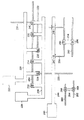
図12は、その領域の表面上およびその下のいくつかの相互接続構造を示す、従来技術の集積回路のある領域の例示的な上面図である。アルミニウム・パッド190、192は、垂直な導電性バイア198、200を介して、下層の(すなわち1つ下のレベルの)メタライゼーション・レベル導電性ランナ194、196にそれぞれ接続される。導電性ランナ194、196は、図5における電力バス146であってもよい。導電性ランナ194、196(図5の導電性ランナ132、134を表わす)より下の相互接続レベル内に配設された導電性ランナ204を、導電性バイア206を介して導電性ランナ196に接続し、さらに導電性バイア208を介して追加の下層の相互接続構造および要素に接続する。
FIG. 12 is an exemplary top view of a region of a prior art integrated circuit showing several interconnect structures on and below the surface of the region.
図13は、本発明の教示に従って構成されたデバイスの表面上およびその下のいくつかの相互接続構造を示す、集積回路デバイスのある領域の例示的な上面図である。本発明の教示は、当業者には認識できるように、任意の数の金属相互接続層を有する集積回路デバイス構造に適用することができる。ただし、「n」は最上部のメタライゼーション・レベルを表し、下層のレベルは、nthレベル、例えばn−1またはn−2レベルと表される。 FIG. 13 is an exemplary top view of a region of an integrated circuit device showing several interconnect structures on and below the surface of the device constructed in accordance with the teachings of the present invention. The teachings of the present invention can be applied to integrated circuit device structures having any number of metal interconnect layers, as will be appreciated by those skilled in the art. However, “n” represents the uppermost metallization level, and the lower level is represented as an n th level, eg, n−1 or n−2 level.
アルミニウム・パッド220は、垂直な導電性バイア226、224を介して、下層のn−1レベル導電性ランナ222、223に接続するための電力バス221(メタライゼーション・レベル「n」すなわち最上のレベル内に形成された)の一体部分をなす。アルミニウム・パッド220を電源に接続すると、前記のパッケージ・リードを介して、電力バス221(図6における電力バス174を表わすことができる)は、導電性ランナ222、223に電力を伝達または分配する。この導電性ランナ222、223は、集積回路の全体にわたって電力を連続的に分配するように、下層の導電性ランナ(図13には図示せず)に接続される。電力バス221は、n−1メタライゼーション・レベルにのみ接続するように示されているが、これは単に例示のためにすぎず、下部のメタライゼーション・レベルへの接続は、一連の垂直の導電性バイアを介して行うことができる。
The
引き続き図13を参照すると、アルミニウム・パッド228は、相互接続構造229の一体部分をなす。相互接続構造229は、垂直の導電性バイア232、234、236を介して、下層のn−1レベル導電性ランナ230に接続される。n−1レベル導電性ランナ230は、さらに導電性バイア240を介してn−2レベル導電性ランナ238に接続される。一例では、アルミニウム・パッド228は、パッケージ・リードを介して集積回路の外部の信号を受け取り、アルミニウム・パッド228に接続された様々な相互接続構造を介して適切なデバイス要素にその信号を供給することができる。
With continued reference to FIG. 13, the
n−レベル導電性ランナ244は、アルミニウム・パッド245の一体部分をなし、導電性バイア247、248に接続され、導電性バイア247、248は、さらに下層の導電性ランナ250(n−iレベル内、ただしi=1〜n−1)に接続される。
The n-level
本発明の第2の実施形態によれば、アルミニウム・パッド層は下層の銅の層に対する相互接続構造を提供する。この相互接続構造はパッドに接続されない。例えば、図13のデバイス上面図にさらに示すように、導電性ランナ280、282(例えば、両方ともn−1レベル内に配設される)は、導電性バイア286、288を介して、相互接続構造284(アルミニウム・パッド層n内に形成される)に接続される。他の例では、導電性ランナ250および導電性ランナ292(例えば、両方ともn−1レベル内に配設される)は、導電性バイア298、296を介して、アルミニウム・パッド層(n)内に形成された相互接続構造294によって接続される。したがって前記の電力バス相互接続構造を提供することに加えて、アルミニウム・パッド層内に下層の銅層に対する相互接続構造(相互接続構造274など)を形成することもできる。その結果、アルミニウム・パッド層を使用して相互接続機能を提供することにより、下層の相互接続層をなくすことができる。
According to a second embodiment of the invention, the aluminum pad layer provides an interconnect structure for the underlying copper layer. This interconnect structure is not connected to the pads. For example, as further shown in the device top view of FIG. 13,
以上、本発明を好ましい実施形態に関して説明してきたが、当業者には理解されるように、本発明の範囲から逸脱することなく、様々な変更を加えることができ、その要素の代わりにそれと等価な要素を使用することができる。本発明の範囲にはさらに、本明細書に記載した様々な実施形態からの要素の任意の組合せも含まれる。また、その本質的な範囲から逸脱することなく、変更を行って特定の状態を本発明の教示に適合させることもできる。したがって、本発明は、本発明を実施するために企図される最良の形態として開示された特定の実施形態のみに限定されず、添付の特許請求の範囲に含まれるすべての実施形態を包含するものである。 Although the present invention has been described with reference to preferred embodiments, it will be understood by those skilled in the art that various modifications can be made without departing from the scope of the present invention and equivalents thereof instead of elements thereof. Elements can be used. The scope of the present invention further includes any combination of elements from the various embodiments described herein. Changes may be made to adapt a particular state to the teachings of the invention without departing from the essential scope thereof. Accordingly, the invention is not limited to the specific embodiments disclosed as the best mode contemplated for carrying out the invention, but encompasses all embodiments that fall within the scope of the appended claims. It is.
Claims (6)
半導体基板上のメタライゼーション相互接続システムと、前記メタライゼーション相互接続システムは誘電体層内に位置付けられる少なくとも第1及び第2相互接続フィーチャーを含み;
前記メタライゼーション相互接続システム上にわたって位置する電力バスと、前記電力バスは前記第1相互接続フィーチャーと接触する第1コンタクトパッド領域を含み、前記第1コンタクトパッド領域は集積回路デバイスの外部に接続するように構成され、第2領域が前記第2相互接続フィーチャーと接触し、前記電力バスの前記第2領域の上面は前記第1コンタクトパッドの上面の上方に位置づけられ;
前記電力バスと同レベルに位置付けられ、前記電力バスと同じ材料を含む信号ルーティング相互接続と;及び
前記第1コンタクトパッド領域の少なくとも一部を露出し、前記第2領域を保護するための、前記電力バスの少なくとも一部上のパッシベーション層とを含むことを特徴とする集積回路デバイス。 An integrated circuit device, the integrated circuit device comprising:
A metallization interconnection system on a semiconductor substrate, the metallization interconnection system includes at least first and second interconnect features are positioned in a dielectric layer;
A power bus located over the metallization interconnect system, the power bus including a first contact pad region in contact with the first interconnect feature, the first contact pad region connecting to an exterior of an integrated circuit device; Configured such that a second region contacts the second interconnect feature, and an upper surface of the second region of the power bus is positioned above an upper surface of the first contact pad ;
A signal routing interconnect positioned at the same level as the power bus and comprising the same material as the power bus; and exposing at least a portion of the first contact pad area and protecting the second area, An integrated circuit device comprising: a passivation layer on at least a portion of the power bus.
Applications Claiming Priority (4)
| Application Number | Priority Date | Filing Date | Title |
|---|---|---|---|
| US46250403P | 2003-04-10 | 2003-04-10 | |
| US60/462504 | 2003-04-10 | ||
| US10/675,258 US7566964B2 (en) | 2003-04-10 | 2003-09-30 | Aluminum pad power bus and signal routing for integrated circuit devices utilizing copper technology interconnect structures |
| US10/675258 | 2003-09-30 |
Related Child Applications (1)
| Application Number | Title | Priority Date | Filing Date |
|---|---|---|---|
| JP2011236296A Division JP2012054588A (en) | 2003-04-10 | 2011-10-27 | Aluminium pad power bus for integrated circuit device using copper technology interconnection structure, and signal routing technology |
Publications (3)
| Publication Number | Publication Date |
|---|---|
| JP2004320018A JP2004320018A (en) | 2004-11-11 |
| JP2004320018A5 JP2004320018A5 (en) | 2007-05-31 |
| JP5258142B2 true JP5258142B2 (en) | 2013-08-07 |
Family
ID=32096363
Family Applications (2)
| Application Number | Title | Priority Date | Filing Date |
|---|---|---|---|
| JP2004114863A Expired - Fee Related JP5258142B2 (en) | 2003-04-10 | 2004-04-09 | Aluminum pad power bus and signal routing technology for integrated circuit devices using copper technology interconnect structures |
| JP2011236296A Pending JP2012054588A (en) | 2003-04-10 | 2011-10-27 | Aluminium pad power bus for integrated circuit device using copper technology interconnection structure, and signal routing technology |
Family Applications After (1)
| Application Number | Title | Priority Date | Filing Date |
|---|---|---|---|
| JP2011236296A Pending JP2012054588A (en) | 2003-04-10 | 2011-10-27 | Aluminium pad power bus for integrated circuit device using copper technology interconnection structure, and signal routing technology |
Country Status (5)
| Country | Link |
|---|---|
| US (1) | US7566964B2 (en) |
| JP (2) | JP5258142B2 (en) |
| KR (1) | KR101084957B1 (en) |
| GB (2) | GB2401245B (en) |
| TW (1) | TWI344685B (en) |
Families Citing this family (14)
| Publication number | Priority date | Publication date | Assignee | Title |
|---|---|---|---|---|
| US7335536B2 (en) | 2005-09-01 | 2008-02-26 | Texas Instruments Incorporated | Method for fabricating low resistance, low inductance interconnections in high current semiconductor devices |
| US8319343B2 (en) * | 2005-09-21 | 2012-11-27 | Agere Systems Llc | Routing under bond pad for the replacement of an interconnect layer |
| US7952206B2 (en) * | 2005-09-27 | 2011-05-31 | Agere Systems Inc. | Solder bump structure for flip chip semiconductor devices and method of manufacture therefore |
| US8552560B2 (en) * | 2005-11-18 | 2013-10-08 | Lsi Corporation | Alternate pad structures/passivation inegration schemes to reduce or eliminate IMC cracking in post wire bonded dies during Cu/Low-K BEOL processing |
| TWI288463B (en) * | 2006-04-26 | 2007-10-11 | Siliconware Precision Industries Co Ltd | Semiconductor package substrate and semiconductor package having the substrate |
| US7888257B2 (en) * | 2007-10-10 | 2011-02-15 | Agere Systems Inc. | Integrated circuit package including wire bonds |
| WO2009058143A1 (en) * | 2007-10-31 | 2009-05-07 | Agere Systems Inc. | Bond pad support structure for semiconductor device |
| US20100289132A1 (en) * | 2009-05-13 | 2010-11-18 | Shih-Fu Huang | Substrate having embedded single patterned metal layer, and package applied with the same, and methods of manufacturing of the substrate and package |
| US8786062B2 (en) | 2009-10-14 | 2014-07-22 | Advanced Semiconductor Engineering, Inc. | Semiconductor package and process for fabricating same |
| US20110084372A1 (en) * | 2009-10-14 | 2011-04-14 | Advanced Semiconductor Engineering, Inc. | Package carrier, semiconductor package, and process for fabricating same |
| US8569894B2 (en) | 2010-01-13 | 2013-10-29 | Advanced Semiconductor Engineering, Inc. | Semiconductor package with single sided substrate design and manufacturing methods thereof |
| TWI411075B (en) | 2010-03-22 | 2013-10-01 | Advanced Semiconductor Eng | Semiconductor package and manufacturing method thereof |
| US8753917B2 (en) * | 2010-12-14 | 2014-06-17 | International Business Machines Corporation | Method of fabricating photoconductor-on-active pixel device |
| JP2013229455A (en) * | 2012-04-26 | 2013-11-07 | Renesas Electronics Corp | Semiconductor device and method for manufacturing the same |
Family Cites Families (40)
| Publication number | Priority date | Publication date | Assignee | Title |
|---|---|---|---|---|
| JPS5851425B2 (en) | 1975-08-22 | 1983-11-16 | 株式会社日立製作所 | Hand tie souchi |
| US4840923A (en) | 1986-04-30 | 1989-06-20 | International Business Machine Corporation | Simultaneous multiple level interconnection process |
| JPH02163960A (en) | 1988-12-16 | 1990-06-25 | Toshiba Corp | Semiconductor device |
| US5719448A (en) | 1989-03-07 | 1998-02-17 | Seiko Epson Corporation | Bonding pad structures for semiconductor integrated circuits |
| JPH05226584A (en) * | 1992-02-12 | 1993-09-03 | Yamaha Corp | Integrated circuit device |
| US5436412A (en) * | 1992-10-30 | 1995-07-25 | International Business Machines Corporation | Interconnect structure having improved metallization |
| JPH0831820A (en) * | 1994-07-19 | 1996-02-02 | Sony Corp | Semiconductor device |
| US6331482B1 (en) * | 1996-06-26 | 2001-12-18 | Micron Technology, Inc. | Method of VLSI contact, trench, and via filling using a germanium underlayer with metallization |
| US6130161A (en) * | 1997-05-30 | 2000-10-10 | International Business Machines Corporation | Method of forming copper interconnections with enhanced electromigration resistance and reduced defect sensitivity |
| JP3660799B2 (en) * | 1997-09-08 | 2005-06-15 | 株式会社ルネサステクノロジ | Manufacturing method of semiconductor integrated circuit device |
| US6448650B1 (en) * | 1998-05-18 | 2002-09-10 | Texas Instruments Incorporated | Fine pitch system and method for reinforcing bond pads in semiconductor devices |
| US6232662B1 (en) * | 1998-07-14 | 2001-05-15 | Texas Instruments Incorporated | System and method for bonding over active integrated circuits |
| US6225207B1 (en) | 1998-10-01 | 2001-05-01 | Applied Materials, Inc. | Techniques for triple and quadruple damascene fabrication |
| US6018187A (en) * | 1998-10-19 | 2000-01-25 | Hewlett-Packard Cmpany | Elevated pin diode active pixel sensor including a unique interconnection structure |
| US6261944B1 (en) | 1998-11-24 | 2001-07-17 | Vantis Corporation | Method for forming a semiconductor device having high reliability passivation overlying a multi-level interconnect |
| TW445616B (en) * | 1998-12-04 | 2001-07-11 | Koninkl Philips Electronics Nv | An integrated circuit device |
| US6756295B2 (en) | 1998-12-21 | 2004-06-29 | Megic Corporation | Chip structure and process for forming the same |
| SG93278A1 (en) | 1998-12-21 | 2002-12-17 | Mou Shiung Lin | Top layers of metal for high performance ics |
| TW426980B (en) * | 1999-01-23 | 2001-03-21 | Lucent Technologies Inc | Wire bonding to copper |
| JP2000216184A (en) * | 1999-01-25 | 2000-08-04 | Sanyo Electric Co Ltd | Semiconductor device and manufacture thereof |
| US20020000665A1 (en) * | 1999-04-05 | 2002-01-03 | Alexander L. Barr | Semiconductor device conductive bump and interconnect barrier |
| JP3542517B2 (en) * | 1999-04-27 | 2004-07-14 | Necエレクトロニクス株式会社 | Semiconductor device |
| US6107185A (en) * | 1999-04-29 | 2000-08-22 | Advanced Micro Devices, Inc. | Conductive material adhesion enhancement in damascene process for semiconductors |
| US6204165B1 (en) | 1999-06-24 | 2001-03-20 | International Business Machines Corporation | Practical air dielectric interconnections by post-processing standard CMOS wafers |
| US6410435B1 (en) * | 1999-10-01 | 2002-06-25 | Agere Systems Guardian Corp. | Process for fabricating copper interconnect for ULSI integrated circuits |
| US6451681B1 (en) * | 1999-10-04 | 2002-09-17 | Motorola, Inc. | Method of forming copper interconnection utilizing aluminum capping film |
| US6198170B1 (en) * | 1999-12-16 | 2001-03-06 | Conexant Systems, Inc. | Bonding pad and support structure and method for their fabrication |
| US6376353B1 (en) * | 2000-07-03 | 2002-04-23 | Chartered Semiconductor Manufacturing Ltd. | Aluminum and copper bimetallic bond pad scheme for copper damascene interconnects |
| US6833604B2 (en) * | 2000-10-03 | 2004-12-21 | Broadcom Corporation | High density metal capacitor using dual-damascene copper interconnect |
| US6348732B1 (en) * | 2000-11-18 | 2002-02-19 | Advanced Micro Devices, Inc. | Amorphized barrier layer for integrated circuit interconnects |
| JP2002222928A (en) * | 2001-01-29 | 2002-08-09 | Sony Corp | Semiconductor device |
| US6649993B2 (en) * | 2001-03-16 | 2003-11-18 | Agilent Technologies, Inc. | Simplified upper electrode contact structure for PIN diode active pixel sensor |
| US6455943B1 (en) * | 2001-04-24 | 2002-09-24 | United Microelectronics Corp. | Bonding pad structure of semiconductor device having improved bondability |
| JP2002329722A (en) * | 2001-04-27 | 2002-11-15 | Nec Corp | Semiconductor device and its manufacturing method |
| US6979896B2 (en) * | 2001-10-30 | 2005-12-27 | Intel Corporation | Power gridding scheme |
| US6798073B2 (en) * | 2001-12-13 | 2004-09-28 | Megic Corporation | Chip structure and process for forming the same |
| US6614091B1 (en) * | 2002-03-13 | 2003-09-02 | Motorola, Inc. | Semiconductor device having a wire bond pad and method therefor |
| US20030218259A1 (en) * | 2002-05-21 | 2003-11-27 | Chesire Daniel Patrick | Bond pad support structure for a semiconductor device |
| JP2004111796A (en) * | 2002-09-20 | 2004-04-08 | Hitachi Ltd | Semiconductor device |
| US6717270B1 (en) * | 2003-04-09 | 2004-04-06 | Motorola, Inc. | Integrated circuit die I/O cells |
-
2003
- 2003-09-30 US US10/675,258 patent/US7566964B2/en not_active Expired - Lifetime
-
2004
- 2004-03-03 GB GB0404852A patent/GB2401245B/en not_active Expired - Fee Related
- 2004-03-03 GB GB0615199A patent/GB2427074B/en not_active Expired - Fee Related
- 2004-03-29 TW TW093108543A patent/TWI344685B/en active
- 2004-04-08 KR KR1020040023990A patent/KR101084957B1/en active IP Right Grant
- 2004-04-09 JP JP2004114863A patent/JP5258142B2/en not_active Expired - Fee Related
-
2011
- 2011-10-27 JP JP2011236296A patent/JP2012054588A/en active Pending
Also Published As
| Publication number | Publication date |
|---|---|
| GB0404852D0 (en) | 2004-04-07 |
| GB2401245A (en) | 2004-11-03 |
| JP2004320018A (en) | 2004-11-11 |
| JP2012054588A (en) | 2012-03-15 |
| KR101084957B1 (en) | 2011-11-23 |
| GB2401245B (en) | 2006-12-20 |
| GB2427074B (en) | 2007-06-27 |
| TW200503168A (en) | 2005-01-16 |
| TWI344685B (en) | 2011-07-01 |
| GB2427074A (en) | 2006-12-13 |
| US7566964B2 (en) | 2009-07-28 |
| KR20040089496A (en) | 2004-10-21 |
| GB0615199D0 (en) | 2006-09-06 |
| US20040201101A1 (en) | 2004-10-14 |
Similar Documents
| Publication | Publication Date | Title |
|---|---|---|
| JP2012054588A (en) | Aluminium pad power bus for integrated circuit device using copper technology interconnection structure, and signal routing technology | |
| US7777333B2 (en) | Structure and method for fabricating flip chip devices | |
| US8390125B2 (en) | Through-silicon via formed with a post passivation interconnect structure | |
| KR100342897B1 (en) | Semiconductor device and method for manufacturing the same | |
| JP5271985B2 (en) | Integrated circuit structure | |
| KR101163974B1 (en) | Routing under bond pad for the replacement of an interconnect layer | |
| KR100659801B1 (en) | Wire bonding to copper | |
| JP4564166B2 (en) | Method for forming wafer passivation layer | |
| US9773736B2 (en) | Intermediate layer for copper structuring and methods of formation thereof | |
| US9324611B2 (en) | Corrosion resistant via connections in semiconductor substrates and methods of making same | |
| US7245025B2 (en) | Low cost bonding pad and method of fabricating same | |
| US6677235B1 (en) | Silicon die with metal feed through structure | |
| US7932187B2 (en) | Method for fabricating a semiconductor device | |
| JPH11312704A (en) | Dual damask having bonding pad | |
| GB2364170A (en) | Dual damascene bond pad structure for lowering stress and allowing circuitry under pads | |
| JP4034482B2 (en) | Multilayer wiring structure and method of manufacturing semiconductor device | |
| KR100787371B1 (en) | Method for producing electrode and semiconductor device | |
| CN110556299B (en) | Semiconductor structure and forming method thereof | |
| US20020068385A1 (en) | Method for forming anchored bond pads in semiconductor devices and devices formed | |
| JP5429764B2 (en) | Chip and chip manufacturing method | |
| KR100606537B1 (en) | Method for forming the metal interconnect of semiconductor device using full back process |
Legal Events
| Date | Code | Title | Description |
|---|---|---|---|
| A521 | Request for written amendment filed |
Free format text: JAPANESE INTERMEDIATE CODE: A523 Effective date: 20070409 |
|
| A621 | Written request for application examination |
Free format text: JAPANESE INTERMEDIATE CODE: A621 Effective date: 20070409 |
|
| A977 | Report on retrieval |
Free format text: JAPANESE INTERMEDIATE CODE: A971007 Effective date: 20100120 |
|
| A131 | Notification of reasons for refusal |
Free format text: JAPANESE INTERMEDIATE CODE: A131 Effective date: 20100125 |
|
| A601 | Written request for extension of time |
Free format text: JAPANESE INTERMEDIATE CODE: A601 Effective date: 20100423 |
|
| A602 | Written permission of extension of time |
Free format text: JAPANESE INTERMEDIATE CODE: A602 Effective date: 20100428 |
|
| A521 | Request for written amendment filed |
Free format text: JAPANESE INTERMEDIATE CODE: A523 Effective date: 20100722 |
|
| RD02 | Notification of acceptance of power of attorney |
Free format text: JAPANESE INTERMEDIATE CODE: A7422 Effective date: 20100722 |
|
| A02 | Decision of refusal |
Free format text: JAPANESE INTERMEDIATE CODE: A02 Effective date: 20110627 |
|
| A521 | Request for written amendment filed |
Free format text: JAPANESE INTERMEDIATE CODE: A523 Effective date: 20111027 |
|
| A911 | Transfer to examiner for re-examination before appeal (zenchi) |
Free format text: JAPANESE INTERMEDIATE CODE: A911 Effective date: 20111212 |
|
| A912 | Re-examination (zenchi) completed and case transferred to appeal board |
Free format text: JAPANESE INTERMEDIATE CODE: A912 Effective date: 20120106 |
|
| A601 | Written request for extension of time |
Free format text: JAPANESE INTERMEDIATE CODE: A601 Effective date: 20120626 |
|
| A602 | Written permission of extension of time |
Free format text: JAPANESE INTERMEDIATE CODE: A602 Effective date: 20120629 |
|
| A521 | Request for written amendment filed |
Free format text: JAPANESE INTERMEDIATE CODE: A523 Effective date: 20130208 |
|
| A61 | First payment of annual fees (during grant procedure) |
Free format text: JAPANESE INTERMEDIATE CODE: A61 Effective date: 20130423 |
|
| FPAY | Renewal fee payment (event date is renewal date of database) |
Free format text: PAYMENT UNTIL: 20160502 Year of fee payment: 3 |
|
| R150 | Certificate of patent or registration of utility model |
Free format text: JAPANESE INTERMEDIATE CODE: R150 |
|
| S111 | Request for change of ownership or part of ownership |
Free format text: JAPANESE INTERMEDIATE CODE: R313113 |
|
| S533 | Written request for registration of change of name |
Free format text: JAPANESE INTERMEDIATE CODE: R313533 |
|
| R350 | Written notification of registration of transfer |
Free format text: JAPANESE INTERMEDIATE CODE: R350 |
|
| R371 | Transfer withdrawn |
Free format text: JAPANESE INTERMEDIATE CODE: R371 |
|
| S111 | Request for change of ownership or part of ownership |
Free format text: JAPANESE INTERMEDIATE CODE: R313113 |
|
| R371 | Transfer withdrawn |
Free format text: JAPANESE INTERMEDIATE CODE: R371 |
|
| S111 | Request for change of ownership or part of ownership |
Free format text: JAPANESE INTERMEDIATE CODE: R313113 |
|
| R350 | Written notification of registration of transfer |
Free format text: JAPANESE INTERMEDIATE CODE: R350 |
|
| LAPS | Cancellation because of no payment of annual fees |