JP5255437B2 - Semiconductor nanowire transistor - Google Patents
Semiconductor nanowire transistor Download PDFInfo
- Publication number
- JP5255437B2 JP5255437B2 JP2008516797A JP2008516797A JP5255437B2 JP 5255437 B2 JP5255437 B2 JP 5255437B2 JP 2008516797 A JP2008516797 A JP 2008516797A JP 2008516797 A JP2008516797 A JP 2008516797A JP 5255437 B2 JP5255437 B2 JP 5255437B2
- Authority
- JP
- Japan
- Prior art keywords
- gate
- contact
- nanowire
- field effect
- drain
- Prior art date
- Legal status (The legal status is an assumption and is not a legal conclusion. Google has not performed a legal analysis and makes no representation as to the accuracy of the status listed.)
- Expired - Fee Related
Links
- 239000002070 nanowire Substances 0.000 title claims description 84
- 239000004065 semiconductor Substances 0.000 title claims description 33
- 239000000463 material Substances 0.000 claims description 51
- 230000005669 field effect Effects 0.000 claims description 31
- 239000012212 insulator Substances 0.000 claims description 16
- 238000009413 insulation Methods 0.000 claims 2
- 230000004888 barrier function Effects 0.000 description 24
- 239000000758 substrate Substances 0.000 description 15
- 238000000034 method Methods 0.000 description 13
- 229910001218 Gallium arsenide Inorganic materials 0.000 description 12
- 229910045601 alloy Inorganic materials 0.000 description 12
- 239000000956 alloy Substances 0.000 description 12
- 238000000151 deposition Methods 0.000 description 8
- 229910000673 Indium arsenide Inorganic materials 0.000 description 7
- 229910052785 arsenic Inorganic materials 0.000 description 7
- 229910052733 gallium Inorganic materials 0.000 description 7
- 229910052738 indium Inorganic materials 0.000 description 7
- RPQDHPTXJYYUPQ-UHFFFAOYSA-N indium arsenide Chemical compound [In]#[As] RPQDHPTXJYYUPQ-UHFFFAOYSA-N 0.000 description 7
- 229910052698 phosphorus Inorganic materials 0.000 description 7
- 229910052782 aluminium Inorganic materials 0.000 description 6
- 230000000694 effects Effects 0.000 description 6
- 229910052751 metal Inorganic materials 0.000 description 6
- 239000002184 metal Substances 0.000 description 6
- 230000005641 tunneling Effects 0.000 description 6
- 229910000577 Silicon-germanium Inorganic materials 0.000 description 5
- 238000013461 design Methods 0.000 description 5
- 230000005684 electric field Effects 0.000 description 5
- 230000010355 oscillation Effects 0.000 description 5
- 230000003071 parasitic effect Effects 0.000 description 5
- 229910005540 GaP Inorganic materials 0.000 description 4
- 230000008021 deposition Effects 0.000 description 4
- WPYVAWXEWQSOGY-UHFFFAOYSA-N indium antimonide Chemical compound [Sb]#[In] WPYVAWXEWQSOGY-UHFFFAOYSA-N 0.000 description 4
- 239000002923 metal particle Substances 0.000 description 4
- 239000000203 mixture Substances 0.000 description 4
- 230000008901 benefit Effects 0.000 description 3
- 230000015556 catabolic process Effects 0.000 description 3
- 238000006731 degradation reaction Methods 0.000 description 3
- 238000005530 etching Methods 0.000 description 3
- 230000008569 process Effects 0.000 description 3
- 238000000927 vapour-phase epitaxy Methods 0.000 description 3
- 229910004205 SiNX Inorganic materials 0.000 description 2
- 238000004891 communication Methods 0.000 description 2
- 239000004020 conductor Substances 0.000 description 2
- 238000005516 engineering process Methods 0.000 description 2
- 238000000407 epitaxy Methods 0.000 description 2
- 230000006872 improvement Effects 0.000 description 2
- 239000002245 particle Substances 0.000 description 2
- 230000009467 reduction Effects 0.000 description 2
- 229920006395 saturated elastomer Polymers 0.000 description 2
- 229910000530 Gallium indium arsenide Inorganic materials 0.000 description 1
- 229910004298 SiO 2 Inorganic materials 0.000 description 1
- RTAQQCXQSZGOHL-UHFFFAOYSA-N Titanium Chemical compound [Ti] RTAQQCXQSZGOHL-UHFFFAOYSA-N 0.000 description 1
- 230000003321 amplification Effects 0.000 description 1
- 229910052787 antimony Inorganic materials 0.000 description 1
- 230000008859 change Effects 0.000 description 1
- 238000004871 chemical beam epitaxy Methods 0.000 description 1
- 150000001875 compounds Chemical class 0.000 description 1
- 230000008878 coupling Effects 0.000 description 1
- 238000010168 coupling process Methods 0.000 description 1
- 238000005859 coupling reaction Methods 0.000 description 1
- 230000003247 decreasing effect Effects 0.000 description 1
- 230000007547 defect Effects 0.000 description 1
- 230000001419 dependent effect Effects 0.000 description 1
- 238000010586 diagram Methods 0.000 description 1
- 239000003989 dielectric material Substances 0.000 description 1
- 238000009792 diffusion process Methods 0.000 description 1
- 230000008020 evaporation Effects 0.000 description 1
- 238000001704 evaporation Methods 0.000 description 1
- 229910052732 germanium Inorganic materials 0.000 description 1
- GNPVGFCGXDBREM-UHFFFAOYSA-N germanium atom Chemical compound [Ge] GNPVGFCGXDBREM-UHFFFAOYSA-N 0.000 description 1
- 239000011810 insulating material Substances 0.000 description 1
- 238000004519 manufacturing process Methods 0.000 description 1
- -1 n ++- Si Inorganic materials 0.000 description 1
- 238000003199 nucleic acid amplification method Methods 0.000 description 1
- 230000003647 oxidation Effects 0.000 description 1
- 238000007254 oxidation reaction Methods 0.000 description 1
- 229910021420 polycrystalline silicon Inorganic materials 0.000 description 1
- 229920000642 polymer Polymers 0.000 description 1
- 238000012545 processing Methods 0.000 description 1
- 230000027756 respiratory electron transport chain Effects 0.000 description 1
- 229910052710 silicon Inorganic materials 0.000 description 1
- 238000012995 silicone-based technology Methods 0.000 description 1
- 238000004544 sputter deposition Methods 0.000 description 1
- 239000000126 substance Substances 0.000 description 1
- 230000008542 thermal sensitivity Effects 0.000 description 1
- 239000010936 titanium Substances 0.000 description 1
- 229910052719 titanium Inorganic materials 0.000 description 1
- 239000012808 vapor phase Substances 0.000 description 1
Images


Classifications
-
- H—ELECTRICITY
- H01—ELECTRIC ELEMENTS
- H01L—SEMICONDUCTOR DEVICES NOT COVERED BY CLASS H10
- H01L29/00—Semiconductor devices adapted for rectifying, amplifying, oscillating or switching, or capacitors or resistors with at least one potential-jump barrier or surface barrier, e.g. PN junction depletion layer or carrier concentration layer; Details of semiconductor bodies or of electrodes thereof ; Multistep manufacturing processes therefor
- H01L29/02—Semiconductor bodies ; Multistep manufacturing processes therefor
- H01L29/06—Semiconductor bodies ; Multistep manufacturing processes therefor characterised by their shape; characterised by the shapes, relative sizes, or dispositions of the semiconductor regions ; characterised by the concentration or distribution of impurities within semiconductor regions
- H01L29/0657—Semiconductor bodies ; Multistep manufacturing processes therefor characterised by their shape; characterised by the shapes, relative sizes, or dispositions of the semiconductor regions ; characterised by the concentration or distribution of impurities within semiconductor regions characterised by the shape of the body
- H01L29/0665—Semiconductor bodies ; Multistep manufacturing processes therefor characterised by their shape; characterised by the shapes, relative sizes, or dispositions of the semiconductor regions ; characterised by the concentration or distribution of impurities within semiconductor regions characterised by the shape of the body the shape of the body defining a nanostructure
-
- B—PERFORMING OPERATIONS; TRANSPORTING
- B82—NANOTECHNOLOGY
- B82Y—SPECIFIC USES OR APPLICATIONS OF NANOSTRUCTURES; MEASUREMENT OR ANALYSIS OF NANOSTRUCTURES; MANUFACTURE OR TREATMENT OF NANOSTRUCTURES
- B82Y10/00—Nanotechnology for information processing, storage or transmission, e.g. quantum computing or single electron logic
-
- H—ELECTRICITY
- H01—ELECTRIC ELEMENTS
- H01L—SEMICONDUCTOR DEVICES NOT COVERED BY CLASS H10
- H01L29/00—Semiconductor devices adapted for rectifying, amplifying, oscillating or switching, or capacitors or resistors with at least one potential-jump barrier or surface barrier, e.g. PN junction depletion layer or carrier concentration layer; Details of semiconductor bodies or of electrodes thereof ; Multistep manufacturing processes therefor
- H01L29/02—Semiconductor bodies ; Multistep manufacturing processes therefor
- H01L29/06—Semiconductor bodies ; Multistep manufacturing processes therefor characterised by their shape; characterised by the shapes, relative sizes, or dispositions of the semiconductor regions ; characterised by the concentration or distribution of impurities within semiconductor regions
- H01L29/0657—Semiconductor bodies ; Multistep manufacturing processes therefor characterised by their shape; characterised by the shapes, relative sizes, or dispositions of the semiconductor regions ; characterised by the concentration or distribution of impurities within semiconductor regions characterised by the shape of the body
- H01L29/0665—Semiconductor bodies ; Multistep manufacturing processes therefor characterised by their shape; characterised by the shapes, relative sizes, or dispositions of the semiconductor regions ; characterised by the concentration or distribution of impurities within semiconductor regions characterised by the shape of the body the shape of the body defining a nanostructure
- H01L29/0669—Nanowires or nanotubes
- H01L29/0673—Nanowires or nanotubes oriented parallel to a substrate
-
- H—ELECTRICITY
- H01—ELECTRIC ELEMENTS
- H01L—SEMICONDUCTOR DEVICES NOT COVERED BY CLASS H10
- H01L29/00—Semiconductor devices adapted for rectifying, amplifying, oscillating or switching, or capacitors or resistors with at least one potential-jump barrier or surface barrier, e.g. PN junction depletion layer or carrier concentration layer; Details of semiconductor bodies or of electrodes thereof ; Multistep manufacturing processes therefor
- H01L29/02—Semiconductor bodies ; Multistep manufacturing processes therefor
- H01L29/06—Semiconductor bodies ; Multistep manufacturing processes therefor characterised by their shape; characterised by the shapes, relative sizes, or dispositions of the semiconductor regions ; characterised by the concentration or distribution of impurities within semiconductor regions
- H01L29/0657—Semiconductor bodies ; Multistep manufacturing processes therefor characterised by their shape; characterised by the shapes, relative sizes, or dispositions of the semiconductor regions ; characterised by the concentration or distribution of impurities within semiconductor regions characterised by the shape of the body
- H01L29/0665—Semiconductor bodies ; Multistep manufacturing processes therefor characterised by their shape; characterised by the shapes, relative sizes, or dispositions of the semiconductor regions ; characterised by the concentration or distribution of impurities within semiconductor regions characterised by the shape of the body the shape of the body defining a nanostructure
- H01L29/0669—Nanowires or nanotubes
- H01L29/0676—Nanowires or nanotubes oriented perpendicular or at an angle to a substrate
-
- H—ELECTRICITY
- H01—ELECTRIC ELEMENTS
- H01L—SEMICONDUCTOR DEVICES NOT COVERED BY CLASS H10
- H01L29/00—Semiconductor devices adapted for rectifying, amplifying, oscillating or switching, or capacitors or resistors with at least one potential-jump barrier or surface barrier, e.g. PN junction depletion layer or carrier concentration layer; Details of semiconductor bodies or of electrodes thereof ; Multistep manufacturing processes therefor
- H01L29/02—Semiconductor bodies ; Multistep manufacturing processes therefor
- H01L29/06—Semiconductor bodies ; Multistep manufacturing processes therefor characterised by their shape; characterised by the shapes, relative sizes, or dispositions of the semiconductor regions ; characterised by the concentration or distribution of impurities within semiconductor regions
- H01L29/0657—Semiconductor bodies ; Multistep manufacturing processes therefor characterised by their shape; characterised by the shapes, relative sizes, or dispositions of the semiconductor regions ; characterised by the concentration or distribution of impurities within semiconductor regions characterised by the shape of the body
- H01L29/0665—Semiconductor bodies ; Multistep manufacturing processes therefor characterised by their shape; characterised by the shapes, relative sizes, or dispositions of the semiconductor regions ; characterised by the concentration or distribution of impurities within semiconductor regions characterised by the shape of the body the shape of the body defining a nanostructure
- H01L29/0669—Nanowires or nanotubes
- H01L29/068—Nanowires or nanotubes comprising a junction
-
- H—ELECTRICITY
- H01—ELECTRIC ELEMENTS
- H01L—SEMICONDUCTOR DEVICES NOT COVERED BY CLASS H10
- H01L29/00—Semiconductor devices adapted for rectifying, amplifying, oscillating or switching, or capacitors or resistors with at least one potential-jump barrier or surface barrier, e.g. PN junction depletion layer or carrier concentration layer; Details of semiconductor bodies or of electrodes thereof ; Multistep manufacturing processes therefor
- H01L29/02—Semiconductor bodies ; Multistep manufacturing processes therefor
- H01L29/12—Semiconductor bodies ; Multistep manufacturing processes therefor characterised by the materials of which they are formed
- H01L29/16—Semiconductor bodies ; Multistep manufacturing processes therefor characterised by the materials of which they are formed including, apart from doping materials or other impurities, only elements of Group IV of the Periodic System
- H01L29/161—Semiconductor bodies ; Multistep manufacturing processes therefor characterised by the materials of which they are formed including, apart from doping materials or other impurities, only elements of Group IV of the Periodic System including two or more of the elements provided for in group H01L29/16, e.g. alloys
- H01L29/165—Semiconductor bodies ; Multistep manufacturing processes therefor characterised by the materials of which they are formed including, apart from doping materials or other impurities, only elements of Group IV of the Periodic System including two or more of the elements provided for in group H01L29/16, e.g. alloys in different semiconductor regions, e.g. heterojunctions
-
- H—ELECTRICITY
- H01—ELECTRIC ELEMENTS
- H01L—SEMICONDUCTOR DEVICES NOT COVERED BY CLASS H10
- H01L29/00—Semiconductor devices adapted for rectifying, amplifying, oscillating or switching, or capacitors or resistors with at least one potential-jump barrier or surface barrier, e.g. PN junction depletion layer or carrier concentration layer; Details of semiconductor bodies or of electrodes thereof ; Multistep manufacturing processes therefor
- H01L29/02—Semiconductor bodies ; Multistep manufacturing processes therefor
- H01L29/12—Semiconductor bodies ; Multistep manufacturing processes therefor characterised by the materials of which they are formed
- H01L29/20—Semiconductor bodies ; Multistep manufacturing processes therefor characterised by the materials of which they are formed including, apart from doping materials or other impurities, only AIIIBV compounds
- H01L29/201—Semiconductor bodies ; Multistep manufacturing processes therefor characterised by the materials of which they are formed including, apart from doping materials or other impurities, only AIIIBV compounds including two or more compounds, e.g. alloys
- H01L29/205—Semiconductor bodies ; Multistep manufacturing processes therefor characterised by the materials of which they are formed including, apart from doping materials or other impurities, only AIIIBV compounds including two or more compounds, e.g. alloys in different semiconductor regions, e.g. heterojunctions
-
- H—ELECTRICITY
- H01—ELECTRIC ELEMENTS
- H01L—SEMICONDUCTOR DEVICES NOT COVERED BY CLASS H10
- H01L29/00—Semiconductor devices adapted for rectifying, amplifying, oscillating or switching, or capacitors or resistors with at least one potential-jump barrier or surface barrier, e.g. PN junction depletion layer or carrier concentration layer; Details of semiconductor bodies or of electrodes thereof ; Multistep manufacturing processes therefor
- H01L29/66—Types of semiconductor device ; Multistep manufacturing processes therefor
- H01L29/68—Types of semiconductor device ; Multistep manufacturing processes therefor controllable by only the electric current supplied, or only the electric potential applied, to an electrode which does not carry the current to be rectified, amplified or switched
- H01L29/76—Unipolar devices, e.g. field effect transistors
- H01L29/772—Field effect transistors
- H01L29/775—Field effect transistors with one dimensional charge carrier gas channel, e.g. quantum wire FET
Description
本発明は、ナノスケール寸法のトランジスタ素子に関する。特に本発明は、電流経路の本質的な部材としてナノワイヤあるいはナノワイヤを有するラップゲート電界効果トランジスタに関連する。 The present invention relates to a transistor element having a nanoscale dimension. In particular, the invention relates to nanowires or wrap gate field effect transistors having nanowires as an essential member of the current path.
狭いバンドギャップを持つ半導体材料、本明細書では以下にIII/V半導体と呼ぶInAsやInSbなどは、高い移動度と高い飽和したキャリヤー速度と低い接触抵抗とを有する。これは、これらの材料を高速で低出力の電子回路部品に対する良い候補とさせ、近年、さまざまな半導体素子においてこれらの材料を使用することへの関心がかなり増加している。しかしながら、これらの材料で作られたトランジスタは、しばしば、電流制御が難しい、電流オン/オフ比が小さい、熱の影響を強く受ける、および狭いバンドギャップに関連する大きな出力コンダクタンスを有するなどの欠点がある。さらに、III/V半導体の構造は、好ましくは商業的に注目すべきものであるために既存のシリコンベース技術と互換性があるべきであり、例えば、Si基板上に製造することが可能であるべきである。このことは、従来技術ではSiとIII/V半導体材料との間の大きな格子不整合のために困難である。これらの上記説明した影響は、III/V半導体素子の応用領域を制限し、アナログとディジタル応用の性能を低減する。図1a−cはInAsナノワイヤトランジスタが上記説明した制限であるa)不十分な電流制御、b)不十分な閾値制御、c)不十分な電流オン/オフ比に苦しむデータを示している。 Semiconductor materials with narrow band gaps, such as InAs and InSb, hereinafter referred to as III / V semiconductors, have high mobility, high saturated carrier velocity, and low contact resistance. This makes these materials good candidates for high speed, low power electronic circuit components and in recent years there has been a significant increase in interest in using these materials in various semiconductor devices. However, transistors made of these materials often have drawbacks such as difficult current control, low current on / off ratio, high thermal sensitivity, and high output conductance associated with narrow band gaps. is there. Furthermore, the structure of III / V semiconductors should be compatible with existing silicon-based technology, preferably because it is commercially noteworthy, and should be capable of being fabricated on, for example, a Si substrate It is. This is difficult in the prior art due to the large lattice mismatch between Si and III / V semiconductor material. These above-described effects limit the application area of III / V semiconductor devices and reduce the performance of analog and digital applications. FIGS. 1 a-c show data that InAs nanowire transistors suffer from the above-described limitations: a) insufficient current control, b) insufficient threshold control, c) insufficient current on / off ratio.
典型的な平面の電界効果トランジスター(FET)では、ソース−ドレイン電流は半導体材料の平面層に閉じ込められる。このことは、例えば、双極性トランジスタなどの縦型でなされたような性能を改善するためにチャンネル中の電流経路の向きにヘテロ構造を使用することがFETでは可能とならないことを意味する。また、狭いバンドギャップ材料でヘテロ構造を作るのもまた難しい。なぜなら、III/V半導体では、適切に格子が適合した材料が不足し、Sbベース化合物の問題があり、ゲルマニウムはSiとSiCに対する大きな格子不整合があるからである。 In a typical planar field effect transistor (FET), the source-drain current is confined to a planar layer of semiconductor material. This means that it is not possible for a FET to use a heterostructure in the direction of the current path in the channel in order to improve performance, for example, in a vertical type such as a bipolar transistor. It is also difficult to make a heterostructure with a narrow bandgap material. This is because in III / V semiconductors, there is a shortage of materials suitable for lattice matching and there is a problem of Sb-based compounds, and germanium has a large lattice mismatch with Si and SiC.
半径方向の歪み緩和が製造することができる広範囲の新しい組成物を可能とするので、ナノワイヤの成長はヘテロ構造の設計における新しい可能性を提供する。例えば、サミュエルソン他の米国特許出願第2004/0075464号によって説明されるように、InPを欠陥なしでInAs上に成長させることができる。ワイアに適合した格子でない基板を使用することも可能であり、これは、Si上にIII−V族半導体を集積するためにさらに多くの設計の融通性を提供しルートを開ける。したがって、上記説明された問題は、ナノスケール寸法の素子の使用によって緩和することができる。 Nanowire growth offers new possibilities in heterostructure design, since radial strain relaxation allows a wide range of new compositions that can be produced. For example, InP can be grown on InAs without defects, as described by Samuelson et al., US Patent Application No. 2004/0075464. It is also possible to use a non-lattice substrate that is compatible with the wire, which provides more design flexibility and routes to integrate III-V semiconductors on Si. Thus, the problems described above can be mitigated by the use of nanoscale sized elements.
この文脈において、半導体ナノワイヤは、200nm未満の直径と数μmまでの長さとを有するロッド形状の構造物として定義される。半導体ナノワイヤの成長は色々な方法で成し得る、例えば、サミュエルソン他の上記参照された米国出願のように異方性成長を促進するために金属粒子を使用する気相エピタキシー(VPE)によってなし得る。 In this context, semiconductor nanowires are defined as rod-shaped structures having a diameter of less than 200 nm and a length of up to several μm. The growth of semiconductor nanowires can be accomplished in a variety of ways, for example, by vapor phase epitaxy (VPE) using metal particles to promote anisotropic growth as in the above referenced US application by Samuelson et al. obtain.
ナノワイヤ形状のFET(矢沢他、米国特許第5,362,972号)において、ナノワイヤ電界効果トランジスタが説明される。ゲートは狭いナノワイヤを取り囲み、良いゲートカップリングを提供し、ラップゲートFETを形成している。ナノワイヤは、気相法によって成長された均質のGaAsウィスカーである。 Nanowire field effect transistors are described in nanowire shaped FETs (Yazawa et al., US Pat. No. 5,362,972). The gate surrounds the narrow nanowire, provides good gate coupling, and forms a wrap gate FET. Nanowires are homogeneous GaAs whiskers grown by a vapor phase method.
先行技術のナノワイヤトランジスタは、半導体ナノワイヤを使用する可能性を示している。しかしながら、例えばIon/Ioffや衝突イオン化速度などに関する実験的発見は、商業的に魅力的な素子を提供できる前に改良が必要であることを示している。接触抵抗は速度と出力電力とを落とし電力消費を増すので、半導体素子との接点は特別に関心がある領域である。
明らかに、先行技術のラップゲートFETトランジスタは、想定されるような高速で低い電力の電子回路部品における機能ユニットとして機能するためにはかなりの改善を必要とする。 Clearly, prior art wrap gate FET transistors require significant improvement to function as functional units in high speed, low power electronic circuit components as envisioned.
本発明の目的は、先行技術のトランジスタの欠点を克服するラップゲートFETトランジスタを提供することである。これは、請求項1で定められるような素子によって達成される。
It is an object of the present invention to provide a wrap gate FET transistor that overcomes the shortcomings of prior art transistors. This is achieved by an element as defined in
本発明によると、半導体ナノワイヤに基づくラップ絶縁体ゲート電界効果トランジスタ(WIGFET)が提供される。FETの電流チャネルは第1バンドギャップを持つ材料からなる半導体ナノワイヤを含んでいる。ソース接点はナノワイヤの一方の端部に配置され、ドレイン接点は反対の端部に配置される。ラップゲート接点は、ソース接点とドレイン接点との間のナノワイヤの一部を取り囲こみ、ゲート領域を定める。本発明に基づくFETトランジスタのナノワイヤは、第2バンドギャップを持つ材料の少なくとも1つのセグメントである少なくとも1つのヘテロ構造を提供し、第2バンドギャップはナノワイヤのバンドギャップ(第1バンドギャップ)と異なっている。ヘテロ構造の少なくとも1つは、ソース接点、ドレイン接点またはゲート接点のうちの1つと連結すべきである。 According to the present invention, a wrap insulator gate field effect transistor (WIGFET) based on semiconductor nanowires is provided. The current channel of the FET includes a semiconductor nanowire made of a material having a first band gap. The source contact is located at one end of the nanowire and the drain contact is located at the opposite end. The wrap gate contact surrounds a portion of the nanowire between the source and drain contacts and defines a gate region. The nanowire of the FET transistor according to the present invention provides at least one heterostructure that is at least one segment of a material having a second band gap, the second band gap being different from the nanowire band gap (first band gap). ing. At least one of the heterostructures should be coupled to one of a source contact, a drain contact or a gate contact.
本発明の1つの実施例によると、ヘテロ構造はナノワイヤと接点との間の接触抵抗を低減するために、ソース接点および/またはドレイン接点との連絡を提供する。通常この連絡は、ナノワイヤ材料より狭いバンドギャップを持つ材料のセグメントを提供することによって達成される。金属−半導体接点は狭いバンドギャップを持つ材料のために低い障壁高さを形成するので、ラップゲートFETのソースとドレイン接点などの素子接点にこれらの材料を使うことは魅力的である。 According to one embodiment of the present invention, the heterostructure provides communication with the source and / or drain contacts to reduce the contact resistance between the nanowire and the contacts. This communication is usually accomplished by providing a segment of material that has a narrower band gap than the nanowire material. Since metal-semiconductor contacts form a low barrier height for materials with a narrow band gap, it is attractive to use these materials for device contacts such as the source and drain contacts of a wrap gate FET.
本発明の別の実施例によると、ヘテロ構造は、ゲート領域中に少なくとも部分的に導入され、トランジスタの能動パーツとなる。ヘテロ構造は、ナノワイヤより広いバンドギャップを持つ材料の一個以上のセグメントを含み、トランジスタの性能の異なる態様を最適化するためにその性質を変えることができるバリアを形成する。例えば、ヘテロ構造は、トランジスタの衝突イオン化速度を減少させるために、または、オフ/オフ電流特性を改良するために、およびドレイン誘発障壁低下の影響を減少するために導入され得る。 According to another embodiment of the invention, the heterostructure is at least partially introduced into the gate region and becomes an active part of the transistor. The heterostructure includes one or more segments of a material with a wider bandgap than the nanowire, forming a barrier that can be altered in its properties to optimize different aspects of transistor performance. For example, heterostructures can be introduced to reduce the impact ionization rate of transistors or to improve off / off current characteristics and to reduce the effects of drain induced barrier degradation.
本発明に基づくFETトランジスタにより、高速で低電力の電子回路部品素子を提供することが可能である。ヘテロ構造を含むナノワイヤ技術は工業的製造に対してよく適合している。 The FET transistor according to the present invention can provide a high-speed and low-power electronic circuit component element. Nanowire technology involving heterostructures is well suited for industrial manufacturing.
本発明に基づくFETの1つの利点は、アナログまたはデジタルの応用に対してナノワイヤのゲート領域内またはその近くでヘテロ構造のセグメントの異なる選択によってトランジスタを最適化することができる点である。 One advantage of the FET according to the present invention is that the transistor can be optimized by different selection of heterostructure segments in or near the nanowire gate region for analog or digital applications.
本発明の更なる利点は、ヘテロ構造が低減された衝突イオン化速度による出力コンダクタンスの低減、電流オンオフ比の改良、ドレイン誘発障壁低下の低減によるゲート電圧振動の低減、接触抵抗の低減および熱安定性の増加を可能にするので、FETの性能が向上することである。 Further advantages of the present invention include reduced output conductance due to impact ionization rate with reduced heterostructure, improved current on / off ratio, reduced gate voltage oscillation due to reduced drain induced barrier degradation, reduced contact resistance and thermal stability. FET performance is improved.
本発明の実施例は特許請求範囲の従属項の範囲で定められる。本発明の他の目的、利点および特徴は、添付図面と請求項とに関連して考慮されると、本発明の以下の詳細な説明から明らかになるだろう。 Embodiments of the invention are defined in the dependent claims. Other objects, advantages and features of the present invention will become apparent from the following detailed description of the invention when considered in conjunction with the accompanying drawings and claims.
本発明の好適な実施例は、以下、添付図面を参照して説明されるだろう。本発明に基づくラップゲート型ナノワイヤトランジスタは、その周囲にゲートを後成長処理によって形成される少なくとも1つの縦型ナノワイヤに基づいており、そこでは、従来の電界効果トランジスタ(FET)と類似の電場効果がトランジスタ動作に使用されている。Siより狭いバンドギャップを持つ材料(InAs、InSbおよびIn、As、Ga、Sb、およびPの合金のようなもの)は、増加した移動度と飽和した電子速度によって素子特性を高めるために好ましくはナノワイヤ中で使用される。トランジスタ中のチャンネルとして作用するナノワイヤは、粒子が異方性の成長を促進するのに使用される選択的エピタクシを使用して成長させることができる。化学ビームエピタキシーあるいは異なる種類の気相エピタキシー法を成長のために使用することができる。リソグラフ法あるいは金属粒子堆積法は金属粒子を定めるために使用され、金属粒子のサイズはワイヤの直径を決定する。通常は200nm以下の直径を5%の標準偏差で製造することができる。ワイヤは定められた位置でのみ成長し、平面の成長速度は粒子に支援された成長モードに対してわずかである。半導体基板上にナノワイヤを成長させる適切な方法は米国特許出願第2003/010244号公報に記載されている。ヘテロ構造を持つエピタキシー成長したナノワイヤを提供する方法は、米国特許出願第2004/0075464号公報に記載されている。 Preferred embodiments of the present invention will now be described with reference to the accompanying drawings. The wrap-gate nanowire transistor according to the present invention is based on at least one vertical nanowire formed by a post-growth process with a gate around it, where the field effect is similar to a conventional field effect transistor (FET). Are used for transistor operation. Materials with band gaps narrower than Si (such as InAs, InSb and alloys of In, As, Ga, Sb, and P) are preferably used to enhance device characteristics due to increased mobility and saturated electron velocity. Used in nanowires. Nanowires that act as channels in transistors can be grown using selective epitaxy where the particles are used to promote anisotropic growth. Chemical beam epitaxy or different types of vapor phase epitaxy methods can be used for growth. Lithographic methods or metal particle deposition methods are used to define metal particles, and the size of the metal particles determines the diameter of the wire. Usually, a diameter of 200 nm or less can be produced with a standard deviation of 5%. The wire grows only at defined locations and the planar growth rate is negligible for the particle assisted growth mode. A suitable method for growing nanowires on a semiconductor substrate is described in US Patent Application No. 2003/010244. A method for providing epitaxy grown nanowires with heterostructures is described in US Patent Application No. 2004/0075464.
図2は本発明に基づくラップゲート電界効果トランジスタ200の原理の構図を示す。通常はIII/V半導体であるナノワイヤ205はチャンネルとして提供される。ナノワイヤ205の材料は、ナノワイヤバンドギャップと呼ばれるバンドギャップ、通常は比較的狭いバンドギャップを持つ。ナノワイヤの一端部にはソース接点240が提供され、反対端部にはドレイン接点250が提供される。ソース接点240とドレイン接点250の間にゲート接点260が配置される。ゲート接点260は、ナノワイヤ205を取り囲みまたは包み、ナノワイヤ205のゲート部分206の一部を覆っている。ゲート部分206の中央部とソース接点240との間の部分はゲート・ソース部分207と呼ばれ、ゲート部分206の中央部とドレイン接点250の間の部分はゲートドレイン部分208と呼ばれる。ドレイン接点250はドレイン接点パッド257に接続されている。その代替物として、付加的な接点パッドは必要でなく、ドレイン接点が外部接続のための接続点として機能するようにしてもよい。ナノワイヤ205は基板210上に成長する。基板210は、例えば、S.I.GaAs、S.I.InP、Si、n+-InP、またはSOIである得る。基板はトランジスタ中で低アクセス抵抗を達成するためにn++-InP、n++-GaAs、n++-Si、ポリーSiなどの2次元エピタキシャル層211で提供され得る。ナノワイヤ205は、好ましくはInPまたはGaAsのSI基板上で成長され得る。また、層211は省略され得る。基板210はソース接点240を形成し得る。その代替物として、専用のソース接点240がパターン層212の形態で基板表面に提供される。パターン層212はゲート接点とゲートパッドの寄生容量(parasitic capacitance)を減少させる。アクセス抵抗をさらに減少させるためにパターン層242の一部を金属膜と交換し得る。基板210、任意のエピタキシャル層211およびパターン層212はトランジスタ200の導電領域を形成する。全外部の電気接点が同じ平面でなされることが要求される場合、導電材料のソース接点パッド215が終端となる柱(pillar)213が形成され得る。ソース接点パッド215は、ドレイン接点パッド257と同じ面に配置される。その代替物として、柱は、ソース接点240と同じ平面におけるドレインにアクセスするのに使用され得る。ドレイン接点とソース接点の両方は、ナノワイヤ205との良い電気接点を確実にするために好ましくはナノワイヤの外側の円筒表面上に一部が延びているであろう。ドレイン接点は寄生を抑えるためにエアブリッジ技術で形成されるかもしれないが、SiNxなどの絶縁性の無機膜または有機膜から化学的および機械的に安定した層がドレインと基板の間の絶縁体として使用され得る。この層は、トップ接点が形成される前にワイヤのトップから遠くにエッチングされる。図示されたデザインの代替物として、全外部の接点を素子の基板側面上に作ることができ、その結果として、ゲート接点260とドレイン接点250は柱または類似の構造物を通して接続され、その接点から基板210の上面で定められる平面まで延びる。
FIG. 2 illustrates the principle composition of a wrap gate
ゲート接点260は、ナノワイヤ205を取り囲こみ、5〜500nmの長さを有する。ゲート接点260は、電導部261と通常1〜50nmの厚さの絶縁層262とからなり、絶縁層262は基板とナノワイヤ205からゲート接点260の電導部261を隔離する。したがって、形成されたトランジスタのタイプは、金属絶縁体半導体電界効果トランジスタ(MISFET)である。ラップゲートを与えた本発明に基づくトランジスタは、ラップ絶縁体ゲート電界効果トランジスタ(WIGFET)と呼ぶことができる。SiNxあるいはSiO2が絶縁体として使用され得るが、高κ誘電体を含む異なる絶縁材料は使用可能である。絶縁層は堆積法によってあるいはワイヤの周囲を半径方向に成長した半導体層の酸化によって形成され得る。また、場合によっては絶縁層と組み合わせて、チャンネルからゲートを分離するためにチャネル領域のバンドギャップよりも広いバンドギャップのエピタキシ成長した半導体層(コア/シェルナノワイヤ)を使用することも可能である。この場合のレイアウトは縦型金属半導体電界効果トランジスタ(MESFET)あるいは縦型高電子移動トランジスタ(HEMT)に類似している。
The
ゲート接点260は多くの堆積によって形成され、エッチング工程は、半導体基板上へのワイヤの成長、制御された厚さを有するゲート絶縁体の堆積、スパッタリングを経由するゲート金属の堆積、蒸着または化学的堆積、有機膜のスピンオン法、ゲート長を定めるためにポリマーのエッチバック、ゲート金属の湿式エッチングを含む。これらの工程後に、図2に示されているように、ゲートがワイヤの基部周囲をくるむ。ゲート接点260の外部接続のためにゲート接点構造265が提供される。通常、好ましくはゲート接点構造265の端部は、同じ平面でドレイン端末257としてのゲート接点パッド267に連絡する。当技術分野での当業者に理解されるように、上記概説された手続きは例示であり、ラップゲートを提供するための代替手法は当業者によく知られている。
The
ドレイン接点250のエアブリッジは、それがワイヤのトップの周囲を巻き付けるように製造される。これは電流チャネルのサイズと比べて大きい接点面を与える。チタンの薄い接点層は、半導体表面に対する金属の接着を高めて接触抵抗を減少させるために使用され得る。
The air bridge of the
この応用の目的のために、用語「接点(contact)」は限定無しに外部電圧あるいは外部電流が印加される好ましくは高い導電材料であり、また、例えば、ドレイン接点、ソース接点またはゲート接点の一部であるエアブリッジ、絶縁体層、および接合層を含むことも意味する。 For the purpose of this application, the term “contact” is preferably a highly conductive material to which an external voltage or current is applied without limitation, and for example one of a drain contact, a source contact or a gate contact. It is also meant to include an air bridge, an insulator layer, and a bonding layer.
図2に示された実施において、ラップゲートを有するたった1つの活性ナノワイヤが示されているが、複数のナノワイヤが平行におかれて所望の駆動電流とトランスコンダクタンスとを得るためにトランジスタ中のチャンネルに結合され得る。 In the implementation shown in FIG. 2, only one active nanowire with a wrap gate is shown, but a plurality of nanowires are placed in parallel to provide a channel in the transistor to obtain the desired drive current and transconductance. Can be combined.
本発明によると、少なくとも1つのヘテロ構造270がナノワイヤ205に提供される。ヘテロ構造材料は、ナノワイヤ205の材料のバンドギャップと比べて異なるバンドギャップを持つはずである。
According to the present invention, at least one
本発明によると、ヘテロ構造はドレイン接点、ソース接点またはゲート接点のうちの少なくともの1つの近くでナノワイヤの性質を変更するべきであり、すなわちヘテロ構造は接点の1つと連結するべきである。各ヘテロ構造が接点の1つと接続している複数のヘテロ構造が提供され得る。更にヘテロ構造は、接点のいずれかに隣接していないナノワイヤ205の一部で実施されるかもしれない。様々なヘテロ構造またはそれらの組合せは、トランジスタの機能の異なる態様を最適化するために導入されるが、それは以下でさらに説明されるだろう。ヘテロ構造セグメントを有するナノワイヤを成長する方法は、上記の参考文献で説明されたように、当技術分野で知られている。
According to the present invention, the heterostructure should change the properties of the nanowire near at least one of the drain contact, the source contact or the gate contact, i.e. the heterostructure should be connected to one of the contacts. Multiple heterostructures can be provided, each heterostructure connected to one of the contacts. Furthermore, the heterostructure may be implemented with a portion of the
本発明の第1実施例によると、1つのヘテロ構造370は、ドレイン接点250あるいはソース接点240のどちらかと連結して提供される、またはあるいはまた2つのヘテロ構造370が提供され、図3に示すように、1つはドレイン接点250と連結し、1つはソース接点240と連結する。ヘテロ構造370は隣接するナノワイヤ205の一部あるいは部分とは異なる構成物の半導体材料のセグメントからなる。ヘテロ構造セグメント370の材料は、ナノワイヤ(InAs、InSb、InGaAsまたはGe、またはAl,Ga、In、As、Pを含む合金のようなもの)より狭いバンドギャップを持つ。セグメントに対する適切なバンドギャップは200〜500MeVの範囲でありセグメント長は50〜300nmである。適切な材料は限定無しにInAs、InSb、Geおよびそれらの組合せおよび合金を含んでいる。ヘテロ接合は、階段または傾斜であり得る。狭いバンドギャップは、トランジスタに対する固有接触抵抗を低減して性能を向上させる。これらのセグメントは、好ましくはさらに接触抵抗を抑えるためにナノワイヤトランジスタの他の部分より高いレベルでドーピングされる。減少した接触抵抗は、トランジスタ特性における飽和領域に達するために要求されるソースドレイン電圧を下げる。ナノワイヤの成長の間のセグメントの導入以外に、トランジスタの処理は均質チャンネルを有する素子の対してと同じである。また、接触抵抗の減少のためのこの実施は、Si、GaAs類似物、InP、GaN、InNおよびSiと匹敵するまたはより大きなバンドギャップを持つナノワイヤを使用することができる。
According to the first embodiment of the present invention, one
本発明の第2実施例によると、ヘテロ構造470は、ゲートとドレインの間、すなわちゲート−ドレイン部208の高電界領域に提供され、図4に示すように、ゲート接点260の外側のドレイン方向に延びている。ヘテロ構造はナノワイヤ(Si、SiGe、InP、GaAs、GaP、またはAl,Ga、In、As、P含有合金のようなもの)より広いバンドギャップ(ΔEgが100meV〜2eV)を有する半導体材料のセグメント(長さ50〜500nm)を含む。適切な材料は限定無しにInP、GaAs、AlAsおよびそれらの組合せおよびそれらの合金を含んでいる。増加したバンドギャップは増加したバンドギャップおよび/または減少した電界により衝突イオン化速度を減少させる。ヘテロ構造は、傾斜または階段であり得る。
According to the second embodiment of the present invention, the
本発明の3番目の実施例によると、ヘテロ構造570はゲート領域209内に提供される、すなわち図5に示すように、ラップゲート接点260によって取り囲まれたナノワイヤの一部中に提供される。ヘテロ構造はナノワイヤ(Si、SiGe、InP、GaAs、GaP、またはAl、Ga、In、As、Pを含む合金のようなもの)より広いバンドギャップ(ΔEcが100〜300meV)を持つ半導体材料のセグメントから成る。セグメントのための適切な材料は限定無しにInP、GaAs、AlAsおよびその組合せおよびその合金を含む。増加したバンドギャップは最大障壁高さ(ほぼEg)を高める。最大障壁高はトランジスタのオフ状態における熱電流を遮蔽するために使用され、電流のオン/オフ比を増加し得る。ヘテロ接合は界面を横切る拡散のような移送(電界補助トンネリング)を可能にするように十分に厚い(5nmより大きい)。ヘテロ接合は、階段または傾斜であり得る。オン電流はヘテロ構造の界面を横切るトンネリングと熱電子放出により高いままで残っている。また、バリアの導入は、トランジスタの閾値電圧Vtを制御するのに使用され得る。素子の熱安定性は、真性キャリアー濃度が−qEg/2kTに比例するので素子のバンドギャップに関連する。広いバンドギャップを持つセグメントの導入は、使用されたドーピングレベルよりかなり低くキャリアー濃度に対する熱的影響を低減するので、素子の熱安定性が増加する。
According to a third embodiment of the present invention, the
本発明の第4実施例によると、図6に示すように、ヘテロ構造670がゲート領域209内に提供される。ヘテロ構造はナノワイヤ(Si、SiGe、InP、GaAs、GaP、またはAl,Ga、In、As、Pを含む合金のようなもの)より広いバンドギャップ(ΔEcが300meVから1eV)を有する半導体材料のセグメントから成る。ヘテロ接合はバリアを横切る量子トンネルを可能にするために充分に薄い(5nm未満)。増加したバンドギャップは最大障壁高さ(ほぼEg)を高める。最大障壁高はトランジスタのオフ状態における熱電流を遮蔽するために使用され、電流のオン/オフ比を増加し得る。ヘテロ接合は、階段または傾斜であり得る。オン電流はヘテロ構造の界面を横切るトンネリングと熱電子放出により高いままで残っている。
According to a fourth embodiment of the present invention, a
本発明の第5実施例によると、図7に示すように、ゲート領域209中に複数のセグメント771、772を含むヘテロ構造770が提供される。ヘテロ構造はナノワイヤ(Si、SiGe、InP、GaAs、GaP、またはAl,Ga、In、As、Pを含む合金のようなもの)より広いバンドギャップを持つ半導体材料のいくつかのセグメントからなる。ヘテロ接合は、トンネリング確率を抑圧するバリアと厚いセグメント771(ΔEcが10meV〜50meV)を横切る量子トンネルを可能にするために充分に薄い(5nm未満)ナノワイヤ205の材料より大きい100meV〜10eV(ΔEc)であるバンドギャップを持つ材料のセグメント772を含む。増加したバンドギャップは最大障壁高さ(ほぼEg)を高める。最大障壁高はトランジスタのオフ状態における熱電流を遮蔽するために使用され、電流のオン/オフ比を増加し得る。ヘテロ接合は、階段または傾斜であり得る。オン電流はヘテロ構造の界面を横切るトンネリングと熱電子放出により高いままで残っている。
According to a fifth embodiment of the present invention, a
本発明の第6実施例によると、図8に示すように、ゲート領域206中およびゲート・ソース部分207中にヘテロ構造870が提供される。ヘテロ構造はナノワイヤ(Si、SiGe、InP、GaAs、GaP、またはAl,Ga、In、As、Pを含む合金のようなもの)より広いバンドギャップで半導体材料のセグメントから成る。ヘテロ接合は階段または傾斜(abrupt or graded)であり得る。ヘテロ構造における階段のバンドオフセットは、ドレイン誘導電場によって下げられないので、一定のバリアを提供する。それは、ドレイン誘発障壁低下の影響を減少させて、トランジスタ特性のサブ閾値の傾斜を増加する。
According to a sixth embodiment of the present invention, a
説明されたように、ヘテロ構造は異なる実施のためにトランジスタを最適化するために、トランジスタチャンネル中に、すなわちナノワイヤ205中に導入することができる。例えば、増幅目的のために使用されるような高周波アナログ演算のためのトランジスタおよび迅速な低動力論理回路で使用するトランジスタは、本発明に基づくトランジスタの実施の2つの極端な場合として考えることができる。ディジタル回路における高速と低電力動作の間のトレードオフにおいて、高い移動度を有する材料は回路スピードの損失なしで供給電圧の低減を可能にする。その結果、低減された供給電圧は特定の操作のための回路動力消費を下げる。あるいはまた、その材料性能は、電力消費を考慮することなくたぶんアナログ回路のスピード性能を高めるためにのみ使用される。
As described, heterostructures can be introduced into the transistor channel, ie,
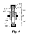
図9において、アナログ応用のために最適化された本発明に基づくWIGFETが示される。狭いバンドギャップを持つヘテロ構造970、971のセグメントは、固有接触抵抗を抑えるためにそれぞれソース領域とドレイン領域に導入される。ヘテロ構造のセグメント970、971は、好ましくは図3を参照して説明された実施例に対応する材料特性を有する。ゲート領域では、高い電界領域における衝突発生プロセスを減少させるために広いバンドギャップ材料からなるセグメント972が導入される。セグメントの長さは通常および好ましくは10〜500nm以内であり、セグメントの半導体材料のバンドギャップはナノワイヤより大きい100meV〜2eV(ΔEg)である。セグメントのための適切な材料は限定無しにInP、GaAs、AlAsおよびその組合せ、およびその合金を含む。セグメントはドレイン領域に向かって延びていて、電場の強さに適合する組成を有する。これは、出力電力を最適化するために出力コンダクタンスを減少させて、増加したドレインバイアスを可能にする。
In FIG. 9, a WIGFET according to the present invention optimized for analog applications is shown. Segments of
図10において、デジタル操作のために最適化された本発明に基づくWIGFETが示される。狭いバンドギャップを持つヘテロ構造1070、1071のセグメントは、固有接触抵抗を抑えるために、それぞれソースとドレイン領域に導入される。ヘテロ構造のセグメント1070、1071は、好ましくは図3を参照して説明された実施例に対応する材料特性を有する。ゲート領域では、オフ電流を低減するためにおよび所与の電流オン/オフ比に達するために要求されるゲート電圧振動を最小にするために広いバンドギャップ材料のセグメント1072が導入される。セグメント材料のバンドギャップはナノワイヤより大きい300meV〜1eV(ΔEc)であるべきである。セグメントはバリアを横切るトンネリングを可能にするために十分薄く(5nm未満)作られるべきであり、適当な材料は、制限無しにInP、GaAs、AlAs、その組合せおよびその合金を含んでいる。
In FIG. 10, a WIGFET according to the present invention optimized for digital operation is shown. Segments of
本発明に基づくナノワイヤ205より広いバンドギャップを持つ材料からなる少なくとも1つのセグメントの形態におけるヘテロ構造の導入は、上記実施例で例示されるように、いろいろな方法で電界効果トランジスタの性質と特性に影響する。図11において、ゲート長の関数としてのサブしきい値電圧振動は、ゲート領域206中で提供された異なる長さのセグメント、b0はセグメント無し、b25は25nm、b50は50nm、b75は75nmとして例示される。バリアセグメントの導入は明確に特定のゲート長のためのサブしきい値電圧振動を抑える。したがって、ナノメータ構造における与えられた設計制限に有利である短いゲートは性能を損なわずに使用することができる。
The introduction of the heterostructure in the form of at least one segment made of a material having a wider bandgap than the
図12において、Ion/Ioff比がゲート領域206中にバリアセグメントを導入することによってどのように改良されたかを示している。
FIG. 12 shows how the Ion / Ioff ratio has been improved by introducing a barrier segment in the
トランジスタの高周波(RF)性能を改良するために寄生容量と抵抗を抑えなければならない。説明された実施では、ゲート長(t)はリソグラフの輝線幅によって制御されるのではなく、堆積とエッチング条件によって制御される。これは、従来のトランジスタ設計と対照的に堆積とエッチング法の制御によってトランジスタのスケーリングを可能とする。ソース領域とドレイン領域の長さは、寄生的なゲート・ソースとゲート・ドレイン容量を減少させるために好ましくは最適化されるが、同時に、ワイヤの全長はトランジスタ中のアクセス抵抗を減少させるために充分に短かくあるべきである。特に外部接点手段、例えば、導電層212、およびソース接点240とドレイン250とゲート接点265にそれぞれ接続するゲート接触構造265およびドレイン接触構造255は、できるだけ狭くして、その領域のオーバレイが最小にされる横木(クロスバー)構造で配置されるべきである。これらの対策は寄生容量を最小にするだろう。
In order to improve the high frequency (RF) performance of the transistor, parasitic capacitance and resistance must be suppressed. In the described implementation, the gate length (t) is not controlled by lithographic emission line width, but by deposition and etching conditions. This allows transistor scaling by controlling deposition and etching methods as opposed to conventional transistor designs. The length of the source and drain regions is preferably optimized to reduce parasitic gate-source and gate-drain capacitances, but at the same time, the overall length of the wires is used to reduce access resistance in the transistor. Should be short enough. In particular, the external contact means, eg, the
本発明は主にいくつかの実施例を参照して上記説明された。しかしながら、当業者によって容易に理解されるように、上で開示された実施例以外のソース領域とドレイン領域の変化を含む実施例は、添付の特許請求の範囲で定められるように本発明の範囲の中で等しく可能である。また、上の実施例は異なった応用に対してWIGFETの性能を適合させるためにいろいろな方法と組み合わされ得ることに注意するべきである。 The present invention has been described above primarily with reference to several embodiments. However, as will be readily appreciated by those skilled in the art, embodiments including source and drain region variations other than those disclosed above are within the scope of the present invention as defined in the appended claims. Is equally possible in It should also be noted that the above embodiments can be combined with various methods to adapt the performance of the WIGFET for different applications.
Claims (10)
前記ナノワイヤの一方の端部に配置されたソース接点(240)と、
前記ナノワイヤの前記一方の端部と反対の端部に配置されたドレイン接点(250)と、
前記ナノワイヤの前記ソース接点と前記ドレイン接点との間の一部分を取り囲こみかつゲート領域(206)を画定するラップゲート接点(260)と、
を有するラップ絶縁体ゲート型電界効果トランジスタであって、
前記ナノワイヤは、ヘテロ構造(270)が生成されるように、第2バンドギャップを持つ材料からなる少なく1つのセグメント(670、1072)をさらに有し、
前記ヘテロ構造は、前記ソース接点(240)、前記ドレイン接点(250)または前記ラップゲート接点(260)のうちの1つと連結し、
前記第2バンドギャップは、前記第1バンドギャップより広く、
前記ヘテロ構造(270)は、少なくとも一部が前記ゲート領域(206)内に配置されている、
ことを特徴とするラップ絶縁体ゲート型電界効果トランジスタ。 A semiconductor nanowire (205) made of a material having a first band gap and forming a current channel of the transistor;
A source contact (240) disposed at one end of the nanowire;
A drain contact (250) disposed at an end opposite the one end of the nanowire;
A wrap gate contact (260) surrounding a portion of the nanowire between the source contact and the drain contact and defining a gate region (206) ;
A wrap insulator gate type field effect transistor having
The nanowire further comprises at least one segment (670, 1072) of a material having a second band gap so that a heterostructure (270) is created ;
The heterostructure is coupled to one of the source contact (240), the drain contact ( 250 ) or the wrap gate contact (260) ;
The second band gap is wider than the first band gap,
The heterostructure (270) is at least partially disposed within the gate region (206);
A wrap insulator gate type field effect transistor.
第2のヘテロ構造(270)が、前記ソース接点(240)または前記ドレイン接点(250)と連結して配置されていることを特徴とする請求項1または請求項2に記載のラップ絶縁体ゲート型電界効果トランジスタ。 At least one of the first heterostructure (270) but is disposed within a portion of the at least partially the nanowire (205) surrounded by the wrap gate contact (260),
Second heterostructure (270) is, the source contact (240) or the drain contact (250) being disposed in conjunction with characterized Claim 1 or wrap insulation gate according to claim 2 Type field effect transistor.
少なくとも一部が前記ゲート領域内に配置されかつ前記ドレイン領域(205)に延びている少なくとも1つのセグメント(972)であって、前記ナノワイヤ(205)の前記材料より広いバンドギャップを持つ第2材料からなる前記少なくとも1つのセグメント(972)と、
を備えていることを特徴とする請求項1に記載のラップ絶縁体ゲート型電界効果トランジスタ。 Wherein disposed in each of the source region and the drain region, and a plurality of segments of heterostructures made of a first material having the narrower bandgap than the nanowire (205) (970, 971),
And at least one segment at least partially extends in arranged and the drain region (205) on said gate region (972), a second material having the band gap wider than the material of the nanowire (205) Said at least one segment (972) consisting of :
Wrap insulation gate field effect transistor according to claim 1, characterized in that it comprises a.
Applications Claiming Priority (3)
| Application Number | Priority Date | Filing Date | Title |
|---|---|---|---|
| SE0501376 | 2005-06-16 | ||
| SE0501376-8 | 2005-06-16 | ||
| PCT/SE2006/050204 WO2006135336A1 (en) | 2005-06-16 | 2006-06-16 | Semiconductor nanowire transistor |
Publications (2)
| Publication Number | Publication Date |
|---|---|
| JP2008544521A JP2008544521A (en) | 2008-12-04 |
| JP5255437B2 true JP5255437B2 (en) | 2013-08-07 |
Family
ID=37532594
Family Applications (1)
| Application Number | Title | Priority Date | Filing Date |
|---|---|---|---|
| JP2008516797A Expired - Fee Related JP5255437B2 (en) | 2005-06-16 | 2006-06-16 | Semiconductor nanowire transistor |
Country Status (7)
| Country | Link |
|---|---|
| US (2) | US8344361B2 (en) |
| EP (2) | EP1891679A1 (en) |
| JP (1) | JP5255437B2 (en) |
| KR (1) | KR20080025147A (en) |
| CN (1) | CN101273459B (en) |
| AU (1) | AU2006258261A1 (en) |
| WO (2) | WO2006135337A1 (en) |
Cited By (1)
| Publication number | Priority date | Publication date | Assignee | Title |
|---|---|---|---|---|
| US10304964B2 (en) | 2015-12-09 | 2019-05-28 | Samsung Electronics Co., Ltd. | Semiconductor device |
Families Citing this family (58)
| Publication number | Priority date | Publication date | Assignee | Title |
|---|---|---|---|---|
| US7335908B2 (en) | 2002-07-08 | 2008-02-26 | Qunano Ab | Nanostructures and methods for manufacturing the same |
| JP5171161B2 (en) * | 2006-09-15 | 2013-03-27 | アイメック | Nanowire tunnel field effect transistor semiconductor device and manufacturing method thereof |
| CN101595565B (en) | 2006-09-18 | 2013-03-27 | 昆南诺股份有限公司 | Method of producing precision vertical and horizontal layers in a vertical semiconductor structure |
| US8049203B2 (en) | 2006-12-22 | 2011-11-01 | Qunano Ab | Nanoelectronic structure and method of producing such |
| US8183587B2 (en) | 2006-12-22 | 2012-05-22 | Qunano Ab | LED with upstanding nanowire structure and method of producing such |
| EP2095426A4 (en) * | 2006-12-22 | 2012-10-10 | Qunano Ab | Nanoelectronic structure and method of producing such |
| KR20090096704A (en) | 2006-12-22 | 2009-09-14 | 큐나노 에이비 | Led with upstanding nanowire structure and method of producing such |
| US8227817B2 (en) | 2006-12-22 | 2012-07-24 | Qunano Ab | Elevated LED |
| KR20090126311A (en) * | 2007-03-28 | 2009-12-08 | 큐나노 에이비 | Nanowire circuit architecture |
| WO2009003056A2 (en) * | 2007-06-27 | 2008-12-31 | New York University | A nanoscale variable resistor/electromechanical transistor |
| US7868426B2 (en) * | 2007-07-26 | 2011-01-11 | University Of Delaware | Method of fabricating monolithic nanoscale probes |
| JP5228406B2 (en) * | 2007-08-30 | 2013-07-03 | 日本電気株式会社 | Semiconductor device and manufacturing method thereof |
| US7932792B2 (en) * | 2008-02-22 | 2011-04-26 | Nokia Corporation | Nanotube device |
| EP2262723A4 (en) * | 2008-04-15 | 2014-05-14 | Qunano Ab | Nanowire wrap gate devices |
| JP5519118B2 (en) * | 2008-04-18 | 2014-06-11 | 白土 猛英 | Semiconductor device and manufacturing method thereof |
| EP2148374A1 (en) * | 2008-07-23 | 2010-01-27 | University College Cork-National University of Ireland, Cork | A tunnel nanowire transistor |
| FR2935971B1 (en) | 2008-09-16 | 2010-11-19 | Arkema France | BIO-ACRYLIC ACID OF POLYMERIC GRADE AND PROCESS FOR MAKING SAME FROM GLYCEROL |
| SE533531C2 (en) | 2008-12-19 | 2010-10-19 | Glo Ab | Nanostructured device |
| US7902541B2 (en) * | 2009-04-03 | 2011-03-08 | International Business Machines Corporation | Semiconductor nanowire with built-in stress |
| SG177480A1 (en) * | 2009-07-31 | 2012-02-28 | Agency Science Tech & Res | A transistor arrangement and a method of forming a transistor arrangement |
| US8309991B2 (en) | 2009-12-04 | 2012-11-13 | International Business Machines Corporation | Nanowire FET having induced radial strain |
| US8313990B2 (en) | 2009-12-04 | 2012-11-20 | International Business Machines Corporation | Nanowire FET having induced radial strain |
| FR2975532B1 (en) * | 2011-05-18 | 2013-05-10 | Commissariat Energie Atomique | ELECTRICAL CONNECTION IN SERIES OF LIGHT EMITTING NANOWIRES |
| US8592276B2 (en) | 2011-07-08 | 2013-11-26 | Peking University | Fabrication method of vertical silicon nanowire field effect transistor |
| CN102315129B (en) * | 2011-07-08 | 2013-01-16 | 北京大学 | Preparation method of vertical silicon nanowire field effect transistor |
| US8350251B1 (en) | 2011-09-26 | 2013-01-08 | Glo Ab | Nanowire sized opto-electronic structure and method for manufacturing the same |
| WO2013095342A1 (en) * | 2011-12-19 | 2013-06-27 | Intel Corporation | High voltage field effect transistors |
| DE112011105945B4 (en) | 2011-12-19 | 2021-10-28 | Google Llc | Group III-N Nanowire Transistors and Processes for Their Manufacture |
| WO2013095345A1 (en) | 2011-12-19 | 2013-06-27 | Intel Corporation | Group iii-n transistors for system on chip (soc) architecture integrating power management and radio frequency circuits |
| WO2013101004A1 (en) * | 2011-12-28 | 2013-07-04 | Intel Corporation | Contact techniques and configurations for reducing parasitic resistance in nanowire transistors |
| US8648330B2 (en) * | 2012-01-05 | 2014-02-11 | International Business Machines Corporation | Nanowire field effect transistors |
| CN103258738B (en) * | 2012-02-20 | 2016-02-17 | 中芯国际集成电路制造(上海)有限公司 | Superlattice nano line field-effect transistor and forming method thereof |
| FR2991100B1 (en) * | 2012-05-25 | 2014-06-27 | Commissariat Energie Atomique | NANOFIL-BASED TRANSISTOR, PROCESS FOR PRODUCING THE TRANSISTOR, SEMICONDUCTOR COMPONENT INTEGRATING THE TRANSISTOR, COMPUTER PROGRAM, AND RECORDING MEDIUM ASSOCIATED WITH THE MANUFACTURING METHOD |
| CN104603952B (en) | 2012-07-06 | 2017-07-21 | 昆南诺股份有限公司 | Radial nanowire Esaki diode apparatus and method |
| US9142400B1 (en) | 2012-07-17 | 2015-09-22 | Stc.Unm | Method of making a heteroepitaxial layer on a seed area |
| US9041106B2 (en) * | 2012-09-27 | 2015-05-26 | Intel Corporation | Three-dimensional germanium-based semiconductor devices formed on globally or locally isolated substrates |
| US8890119B2 (en) | 2012-12-18 | 2014-11-18 | Intel Corporation | Vertical nanowire transistor with axially engineered semiconductor and gate metallization |
| FR3000612B1 (en) * | 2012-12-28 | 2016-05-06 | Commissariat Energie Atomique | OPTOELECTRONIC MICROFILL OR NANOWIL DEVICE |
| CN105900243A (en) * | 2013-09-27 | 2016-08-24 | 英特尔公司 | Methods to achieve high mobility in cladded III-V channel materials |
| US9437738B2 (en) * | 2014-02-07 | 2016-09-06 | Taiwan Semiconductor Manufacturing Company Ltd. | Field effect transistor with heterostructure channel |
| US10276664B2 (en) * | 2014-02-10 | 2019-04-30 | Taiwan Semiconductor Manufacturing Company Limited | Semiconductor structures and methods for multi-dimension of nanowire diameter to improve drive current |
| US9257527B2 (en) | 2014-02-14 | 2016-02-09 | International Business Machines Corporation | Nanowire transistor structures with merged source/drain regions using auxiliary pillars |
| US9490331B2 (en) * | 2014-06-30 | 2016-11-08 | Taiwan Semiconductor Manufacturing Company Limited | Formation of semiconductor arrangement comprising buffer layer and semiconductor column overlying buffer layer |
| CN104241138A (en) * | 2014-07-31 | 2014-12-24 | 上海华力微电子有限公司 | Nanowire transistor |
| US9349860B1 (en) | 2015-03-31 | 2016-05-24 | Taiwan Semiconductor Manufacturing Company, Ltd. | Field effect transistors and methods of forming same |
| SE1530097A1 (en) | 2015-06-22 | 2016-12-23 | Method for Vertical Gate-Last Process | |
| US10381489B2 (en) | 2015-09-30 | 2019-08-13 | National University Corporation Hokkaido University | Tunnel field effect trasnsistor |
| US10032678B2 (en) | 2015-10-15 | 2018-07-24 | Qualcomm Incorporated | Nanowire channel structures of continuously stacked nanowires for complementary metal oxide semiconductor (CMOS) devices |
| CN108701618B (en) * | 2016-03-30 | 2023-02-28 | 英特尔公司 | Nanowires for transistor integration |
| WO2017171824A1 (en) * | 2016-03-31 | 2017-10-05 | Intel Corporation | High mobility asymmetric field effect transistors with a band-offset semiconductor drain spacer |
| KR101834660B1 (en) * | 2016-08-22 | 2018-03-06 | 한양대학교 산학협력단 | Vertical tunneling field-effect transistor and method of fabricating the same |
| CN108695382B (en) | 2017-04-07 | 2021-07-06 | 中芯国际集成电路制造(上海)有限公司 | Semiconductor device and method for manufacturing the same |
| KR102273365B1 (en) * | 2017-05-12 | 2021-07-06 | 씨투에이엠피에스 에이비 | Vertical metal oxide semiconductor field effect transistor and method of forming same |
| CN109427976B (en) | 2017-08-31 | 2021-04-23 | 京东方科技集团股份有限公司 | Thin film transistor, preparation method thereof, array substrate and display device |
| CN109494249B (en) * | 2017-09-11 | 2022-05-24 | 联华电子股份有限公司 | Semiconductor device and method for manufacturing the same |
| JP7027949B2 (en) * | 2018-02-23 | 2022-03-02 | 富士通株式会社 | Manufacturing method of semiconductor devices, receivers and semiconductor devices |
| JP6954184B2 (en) * | 2018-03-01 | 2021-10-27 | 富士通株式会社 | Manufacturing methods for semiconductor devices, receivers and semiconductor devices |
| CN108598170B (en) * | 2018-05-24 | 2022-07-08 | 厦门半导体工业技术研发有限公司 | Nanowire transistor and manufacturing method thereof |
Family Cites Families (19)
| Publication number | Priority date | Publication date | Assignee | Title |
|---|---|---|---|---|
| JPS61276265A (en) | 1985-05-30 | 1986-12-06 | Nec Corp | Insulated gate type field-effect transistor |
| US5362972A (en) | 1990-04-20 | 1994-11-08 | Hitachi, Ltd. | Semiconductor device using whiskers |
| JPH04335538A (en) * | 1991-05-10 | 1992-11-24 | Mitsubishi Electric Corp | Semiconductor device and manufacture thereof |
| US5313117A (en) * | 1991-07-22 | 1994-05-17 | Nippon Telegraph And Telephone Corporation | Semiconductor logic circuit using two n-type negative resistance devices |
| JP3449116B2 (en) | 1996-05-16 | 2003-09-22 | ソニー株式会社 | Semiconductor device |
| JPH1197673A (en) * | 1997-09-17 | 1999-04-09 | Toshiba Corp | Semiconductor device |
| US7335603B2 (en) * | 2000-02-07 | 2008-02-26 | Vladimir Mancevski | System and method for fabricating logic devices comprising carbon nanotube transistors |
| DE10036897C1 (en) * | 2000-07-28 | 2002-01-03 | Infineon Technologies Ag | Field effect transistor used in a switching arrangement comprises a gate region between a source region and a drain region |
| US6882051B2 (en) * | 2001-03-30 | 2005-04-19 | The Regents Of The University Of California | Nanowires, nanostructures and devices fabricated therefrom |
| DE10118405A1 (en) * | 2001-04-12 | 2002-10-24 | Infineon Technologies Ag | Heterostructure component used in electronic devices comprises a single hetero-nanotube having regions made from nanotube materials having different energy band gaps value |
| EP1278039B8 (en) | 2001-07-16 | 2006-03-15 | RWM Schweiz AG | Safety and arming device and usage thereof |
| US7335908B2 (en) | 2002-07-08 | 2008-02-26 | Qunano Ab | Nanostructures and methods for manufacturing the same |
| WO2004032193A2 (en) * | 2002-09-30 | 2004-04-15 | Nanosys, Inc. | Large-area nanoenabled macroelectronic substrates and uses therefor |
| DE10250829B4 (en) * | 2002-10-31 | 2006-11-02 | Infineon Technologies Ag | Nonvolatile memory cell, memory cell array, and method of making a nonvolatile memory cell |
| DE10250830B4 (en) * | 2002-10-31 | 2015-02-26 | Qimonda Ag | Method for producing a circuit array |
| DE10324752A1 (en) | 2003-05-30 | 2005-01-05 | Infineon Technologies Ag | Semiconductor component used as a diode comprises a charge carrier transition region for transferring and controlling a charge carrier between a first electrode region and a second electrode region |
| AU2004265938B2 (en) * | 2003-08-04 | 2009-07-02 | Nanosys, Inc. | System and process for producing nanowire composites and electronic substrates therefrom |
| DE10335813B4 (en) | 2003-08-05 | 2009-02-12 | Infineon Technologies Ag | IC chip with nanowires |
| US20080230802A1 (en) | 2003-12-23 | 2008-09-25 | Erik Petrus Antonius Maria Bakkers | Semiconductor Device Comprising a Heterojunction |
-
2006
- 2006-06-16 EP EP06748043A patent/EP1891679A1/en not_active Withdrawn
- 2006-06-16 CN CN200680030036.8A patent/CN101273459B/en not_active Expired - Fee Related
- 2006-06-16 KR KR1020087001129A patent/KR20080025147A/en not_active Application Discontinuation
- 2006-06-16 EP EP11175291A patent/EP2383785A3/en not_active Withdrawn
- 2006-06-16 US US11/922,242 patent/US8344361B2/en active Active
- 2006-06-16 JP JP2008516797A patent/JP5255437B2/en not_active Expired - Fee Related
- 2006-06-16 WO PCT/SE2006/050207 patent/WO2006135337A1/en active Application Filing
- 2006-06-16 AU AU2006258261A patent/AU2006258261A1/en not_active Abandoned
- 2006-06-16 WO PCT/SE2006/050204 patent/WO2006135336A1/en active Application Filing
- 2006-06-16 US US11/922,243 patent/US8330143B2/en active Active
Cited By (3)
| Publication number | Priority date | Publication date | Assignee | Title |
|---|---|---|---|---|
| US10304964B2 (en) | 2015-12-09 | 2019-05-28 | Samsung Electronics Co., Ltd. | Semiconductor device |
| US11251312B2 (en) | 2015-12-09 | 2022-02-15 | Samsung Electronics Co., Ltd. | Semiconductor device |
| US11942558B2 (en) | 2015-12-09 | 2024-03-26 | Samsung Electronics Co., Ltd. | Semiconductor device |
Also Published As
| Publication number | Publication date |
|---|---|
| WO2006135336A1 (en) | 2006-12-21 |
| JP2008544521A (en) | 2008-12-04 |
| AU2006258261A1 (en) | 2006-12-21 |
| US8330143B2 (en) | 2012-12-11 |
| CN101273459A (en) | 2008-09-24 |
| EP2383785A2 (en) | 2011-11-02 |
| US20090321716A1 (en) | 2009-12-31 |
| US20090294757A1 (en) | 2009-12-03 |
| CN101273459B (en) | 2013-01-02 |
| EP2383785A3 (en) | 2012-02-22 |
| WO2006135337A1 (en) | 2006-12-21 |
| EP1891679A1 (en) | 2008-02-27 |
| KR20080025147A (en) | 2008-03-19 |
| US8344361B2 (en) | 2013-01-01 |
Similar Documents
| Publication | Publication Date | Title |
|---|---|---|
| JP5255437B2 (en) | Semiconductor nanowire transistor | |
| US8119488B2 (en) | Scalable quantum well device and method for manufacturing the same | |
| US10872972B2 (en) | Vertical tunnel field effect transistor (FET) | |
| US9087896B2 (en) | Method of producing precision vertical and horizontal layers in a vertical semiconductor structure | |
| US8404545B2 (en) | Tunnel field-effect transistor with gated tunnel barrier | |
| JP2528537B2 (en) | Field effect transistor | |
| US8129763B2 (en) | Metal-oxide-semiconductor device including a multiple-layer energy filter | |
| US20080067607A1 (en) | Tunnel effect transistors based on elongate monocrystalline nanostructures having a heterostructure | |
| Cutaia et al. | Vertical InAs-Si gate-all-around tunnel FETs integrated on Si using selective epitaxy in nanotube templates | |
| US8288803B2 (en) | Tunnel field effect devices | |
| JP5171161B2 (en) | Nanowire tunnel field effect transistor semiconductor device and manufacturing method thereof | |
| TWI604604B (en) | Complementary-metal-oxide-semiconductor field-effect transistor and method thereof | |
| JP2009524923A (en) | Tunnel transistor with barrier | |
| Kilpi et al. | Increased breakdown voltage in vertical heterostructure III-V nanowire MOSFETs with a field plate | |
| JPH06342811A (en) | Field effect transistor and its manufacture | |
| TWI647823B (en) | Complementary transistor element structure and manufacturing method thereof | |
| US11201246B2 (en) | Field-effect transistor structure and fabrication method | |
| US11621340B2 (en) | Field-effect transistor structure and fabrication method | |
| KR102055945B1 (en) | Tunnel field-effect transistor of 3 dimension structure and method of manufacturing the same | |
| JP3002291B2 (en) | Semiconductor device | |
| Miao et al. | Towards planar GaAs nanowire array high electron mobility transistor | |
| KR20220062070A (en) | Method of Fabrication of Asymmetric Vertical Nanowire MOSFETs and Asymmetric Vertical Nanowire MOSFETs |
Legal Events
| Date | Code | Title | Description |
|---|---|---|---|
| A621 | Written request for application examination |
Free format text: JAPANESE INTERMEDIATE CODE: A621 Effective date: 20090513 |
|
| A131 | Notification of reasons for refusal |
Free format text: JAPANESE INTERMEDIATE CODE: A131 Effective date: 20120903 |
|
| A977 | Report on retrieval |
Free format text: JAPANESE INTERMEDIATE CODE: A971007 Effective date: 20120913 |
|
| A601 | Written request for extension of time |
Free format text: JAPANESE INTERMEDIATE CODE: A601 Effective date: 20121025 |
|
| A602 | Written permission of extension of time |
Free format text: JAPANESE INTERMEDIATE CODE: A602 Effective date: 20121101 |
|
| A521 | Written amendment |
Free format text: JAPANESE INTERMEDIATE CODE: A523 Effective date: 20130226 |
|
| TRDD | Decision of grant or rejection written | ||
| A01 | Written decision to grant a patent or to grant a registration (utility model) |
Free format text: JAPANESE INTERMEDIATE CODE: A01 Effective date: 20130322 |
|
| A61 | First payment of annual fees (during grant procedure) |
Free format text: JAPANESE INTERMEDIATE CODE: A61 Effective date: 20130419 |
|
| R150 | Certificate of patent or registration of utility model |
Ref document number: 5255437 Country of ref document: JP Free format text: JAPANESE INTERMEDIATE CODE: R150 Free format text: JAPANESE INTERMEDIATE CODE: R150 |
|
| FPAY | Renewal fee payment (event date is renewal date of database) |
Free format text: PAYMENT UNTIL: 20160426 Year of fee payment: 3 |
|
| R250 | Receipt of annual fees |
Free format text: JAPANESE INTERMEDIATE CODE: R250 |
|
| R250 | Receipt of annual fees |
Free format text: JAPANESE INTERMEDIATE CODE: R250 |
|
| R250 | Receipt of annual fees |
Free format text: JAPANESE INTERMEDIATE CODE: R250 |
|
| LAPS | Cancellation because of no payment of annual fees |