JP5248993B2 - Bootstrap circuit - Google Patents
Bootstrap circuit Download PDFInfo
- Publication number
- JP5248993B2 JP5248993B2 JP2008293966A JP2008293966A JP5248993B2 JP 5248993 B2 JP5248993 B2 JP 5248993B2 JP 2008293966 A JP2008293966 A JP 2008293966A JP 2008293966 A JP2008293966 A JP 2008293966A JP 5248993 B2 JP5248993 B2 JP 5248993B2
- Authority
- JP
- Japan
- Prior art keywords
- mos transistor
- voltage
- switch element
- source
- comparator
- Prior art date
- Legal status (The legal status is an assumption and is not a legal conclusion. Google has not performed a legal analysis and makes no representation as to the accuracy of the status listed.)
- Expired - Fee Related
Links
Images


Description
本発明は、昇圧電圧を生成するブートストラップ回路に係り、特に、回路の簡素化、動作の信頼性の向上等を図ったものに関する。 The present invention relates to a bootstrap circuit that generates a boosted voltage, and more particularly to a circuit that simplifies the circuit and improves operational reliability.
従来、この種の一般的なブートストラップ回路としては、図5に示されたものなどが良く知られている。
以下、同図に示された従来回路について説明する。
この従来回路は、Pチャンネルの第1のMOSトランジスタ1A、Nチャンネルの第2及び第3のMOSトランジスタ2A,3Aが、コントロール回路(図5においては「CONT」と表記)4AによりON/OFF制御されることで、ブートストラップキャパシタ5Aの充電が制御されて、必要なブートストラップ電圧が得られるよう構成されてなるものである。
Conventionally, as this type of general bootstrap circuit, the one shown in FIG. 5 is well known.
The conventional circuit shown in FIG.
In this conventional circuit, the P-channel
すなわち、コントロール回路4Aにより、第1のMOSトランジスタ1AがONとされると共に、第2のMOSトランジスタ2AがON、第3のMOSトランジスタ3AがOFFとされると、ブートストラップキャパシタ5は、電源電圧VDDによる充電を受け、電圧VBS-OUT、すなわち、出力端子(図5においては「OUT」と表記)32Aを基準としたブートストラップ電圧端子(図5においては「BS」と表記)33Aにおける電圧は、VBS-OUT≒VDDとなる。
That is, when the
一方、コントロール回路4Aにより、第1のMOSトランジスタ1AがOFFとされると共に、第2のMOSトランジスタ2AがOFF、第3のMOSトランジスタ3AがONとされると、VOUT =VINとなり、VBS≒VIN+VBS-OUT≒VIN+VDDとなる。
ここで、VINは、グランド端子(図5においては「GND」と表記)34Aの電位を基準とした入力電圧端子35Aにおける電圧であり、VBSは、グランド端子34Aの電位を基準としたブートストラップ電圧端子33Aにおける電圧である。
On the other hand, when the
Here, VIN is a voltage at the
図5に示された回路において、”LS1”、”LS2”と表記された回路は、いずれもレベルシフタ回路であり、その基本的構成は同一のものであるが、レベルシフタ回路LS1は、電源電圧VDDから電圧VBSに電圧シフトする回路であり、コントロール回路4Aから出力される第1のMOSトランジスタ1Aに対するON/OFFの制御信号を電圧シフトするものとなっている。
また、レベルシフタ回路LS2は、同じく電源電圧VDDから電圧VBSに電圧シフトする回路であり、コントロール回路4Aから出力される第3のMOSトランジスタ3Aに対するON/OFFの制御信号を電圧シフトするものとなっている。
In the circuit shown in FIG. 5, the circuits denoted by “LS1” and “LS2” are both level shifter circuits, and the basic configuration is the same, but the level shifter circuit LS1 is the power supply voltage VDD. Is a circuit that shifts the voltage from V to VBS, and shifts the ON / OFF control signal for the
The level shifter circuit LS2 is also a circuit that shifts the voltage from the power supply voltage VDD to the voltage VBS, and shifts the ON / OFF control signal for the
図6には、従来回路の他の構成例が示されており、以下、同図を参照しつつ、この従来回路について概括的に説明する。なお、図5に示された構成例と同一の構成要素については、同一の符号を付してその詳細な説明を省略し、以下、異なる点を中心に説明する。
この従来回路は、図5における第1のMOSトランジスタ1Aに代えてダイオード10を用いる構成とした点が、図5に示された従来回路と異なるものであるが、この点を除けば、回路全体の動作は、図5に示された従来回路と同様である。
FIG. 6 shows another configuration example of the conventional circuit. Hereinafter, the conventional circuit will be generally described with reference to FIG. In addition, about the same component as the structural example shown by FIG. 5, the same code | symbol is attached | subjected, the detailed description is abbreviate | omitted, and below, it demonstrates centering on a different point.
This conventional circuit is different from the conventional circuit shown in FIG. 5 in that the
上述の図5、図6に示された従来回路を比較すると、図6に示された従来回路においては、ダイオード10の順方向における電圧降下が生じるため、その分、ブートストラップキャパシタ5Aの充電電圧が低下するのに対して、図5に示された従来回路にあっては、第1のMOSトランジスタ1Aにおける電圧降下が殆ど無いため、第3のMOSトランジスタ3Aのゲートバイアス電圧が小さくなるようなことが回避できるという利点を有するものとなっている。
なお、この種の従来回路としては、特許文献1、特許文献2等に開示されたものがある。
Note that this type of conventional circuit is disclosed in Patent Document 1,
しかしながら、図5に示された従来回路にあっては、上述のように、図6に示された従来回路と比較して、第1のMOSトランジスタ1Aのゲートバイアス電圧の不要な低下が殆ど無いという点で有利ではあるが、第1のMOSトランジスタ1Aを制御するために、LS1が必要となるため、レイアウト面積が大きいものとなるという欠点がある。
However, in the conventional circuit shown in FIG. 5, as described above, there is almost no unnecessary decrease in the gate bias voltage of the
例えば、図7には、レベルシフタ回路LS1の最も簡単な構成例が示されているが、ブートストラップ電圧端子33Aとグランド端子34Aとの間に設けられたMOSトランジスタ6は、グランド端子34Aと動作用電源端子31Aとの間に設けられるトランジスタや、ブーストラップ電圧端子33Aと出力端子32Aとの間に設けられるトランジスタと異なり、ドレイン・ソース間に、高電圧であるVBSが印加されるものとなっている。そのため、MOSトランジスタ6には、高耐圧仕様の特別なトランジスタが必要となり、レイアウト面積の増大を招く。
For example, FIG. 7 shows the simplest configuration example of the level shifter circuit LS1, but the
一方、第1のMOSトランジスタ1AのON/OFFの制御信号は、通常、図5に示された従来回路にあっては、レベルシフト回路LS2から出力される制御信号HG2に同期することになり、VOUTのレベルに関係しない。そのため、上記誤動作の問題を解決することができない。
On the other hand, the ON / OFF control signal of the
また、第1及び第2のMOSトランジスタ1A、2AがONで、第3のMOSトランジスタ3AがOFFの際に、本来であれば、VOUT=VGNDとなり、VBS-OUT≒VDDとなるべきところ、外部環境の影響によってVOUTがVGND+αとなった場合でも、第1のMOSトランジスタ1AがONとされるため、ブートストラップキャパシタ5Aに充電された電荷がα電圧分だけ放電され、VBS-OUT≒VDD−αとなる。
そして、VBS-OUT≒VDD−αとなった場合、αが大きいと、特に、ブートストラップ電圧端子33Aと出力端子32Aの間にある回路の動作に必要な電圧が本来の動作電圧以下になり、そのため誤動作を引き起こすこととなる。
Further, when the first and
When VBS-OUT≈VDD-α, when α is large, the voltage necessary for the operation of the circuit between the
本発明は、上記実状に鑑みてなされたもので、レイアウト面積の縮小と共に、信頼性の高い回路動作を確保することのできるブートストラップ回路を提供するものである。 The present invention has been made in view of the above circumstances, and provides a bootstrap circuit capable of ensuring a highly reliable circuit operation while reducing the layout area.
上記本発明の目的を達成するため、本発明に係るブートストラップ回路は、
第1の電源と出力端子との間に第1のスイッチ素子とブートストラップキャパシタが直列接続される一方、前記出力端子とグランド端子との間に、第2のスイッチ素子が、前記出力端子と第2の電源との間に、第3のスイッチ素子が、それぞれ直列接続され、前記第1乃至第3のスイッチ素子の動作制御によって、前記ブートストラップキャパシタの前記第1のスイッチ素子側の端子にブートストラップ電圧が得られるよう構成されてなるブートストラップ回路において、
前記第1のスイッチ素子に流れる電流を監視し、その監視結果に応じて、前記第1のスイッチ素子のON、OFFを制御する電流監視回路が設けられ、前記電流監視回路は、監視回路用第1乃至第4のMOSトランジスタと、比較器を有し、前記監視回路用第1及び第2のMOSトランジスタは、各々のゲートと、前記監視回路用第2のMOSトランジスタのドレインとが相互に接続される一方、前記監視回路用第1及び第2のMOSトランジスタのソースは共に、前記第1のスイッチ素子としての第1のMOSトランジスタのソースと前記ブートストラップキャパシタの一端に接続され、前記監視回路用第3及び第4のMOSトランジスタは、各々のゲートと、前記監視回路用第4のMOSトランジスタのドレインとが相互に接続される一方、前記監視回路用第3のMOSトランジスタのソースは、前記監視回路用第1のMOSトランジスタのドレインと、また、前記監視回路用第4のMOSトランジスタのソースは、前記監視回路用第2のトランジスタのドレインと、それぞれ接続され、前記監視回路用第3のMOSトランジスタのソースは、前記監視回路用第1のMOSトランジスタのドレインと共に、前記比較器の反転入力端子に接続され、前記監視回路用第3のMOSトランジスタのドレインは、前記第1の電源に接続され、前記監視回路用第4のMOSトランジスタのドレインと出力端子との間には、定電流源が接続され、前記比較器の非反転入力端子には、基準電圧源の負極側が接続され、前記基準電圧源の正極側が前記第1のスイッチ素子としての第1のMOSトランジスタのソースに接続され、前記比較器の出力端子は、前記第1のスイッチ素子としての第1のMOSトランジスタのゲートに接続されてなり、前記ブートストラップ電圧が前記第1の電源の電源電圧を超えた状態にある場合に、前記比較器の非反転入力端子の電圧が前記比較器の反転入力端子の電圧を超えて、前記比較器により論理値Highに相当する信号が出力され、前記第1のスイッチ素子としての第1のMOSトランジスタがOFF状態とされる一方、前記ブートストラップ電圧が前記第1の電源の電源電圧を下回る場合に、前記比較器の反転入力端子の電圧が前記比較器の非反転入力端子の電圧を超えて、前記比較器により論理値Lowに相当する信号が出力され、前記第1のスイッチ素子としての第1のMOSトランジスタがON状態とされるよう構成されてなるものである。
また、上記本発明の目的を達成するため、本発明に係るブートストラップ回路は、第1の電源と出力端子との間に第1のスイッチ素子とブートストラップキャパシタが直列接続される一方、前記出力端子とグランド端子との間に、第2のスイッチ素子が、前記出力端子と第2の電源との間に、第3のスイッチ素子が、それぞれ直列接続され、前記第1乃至第3のスイッチ素子の動作制御によって、前記ブートストラップキャパシタの前記第1のスイッチ素子側の端子にブートストラップ電圧が得られるよう構成されてなるブートストラップ回路において、
前記第1のスイッチ素子の端子間の電圧を監視し、その監視結果に応じて、前記第1のスイッチ素子のON、OFFを制御する電圧監視回路が設けられ、前記電圧監視回路は、ツェナーダイオードと比較器を有し、前記ツェナーダイオードは、そのアノードが前記比較器の反転入力端子に接続されると共に、抵抗器を介して前記第1のスイッチ素子としての第1のMOSトランジスタのドレインに接続される一方、前記ツェナーダイオードのカソードは、前記ブートストラップキャパシタに接続される前記第1のスイッチ素子としての第1のMOSトランジスタのソースに接続され、前記比較器の非反入力端子は、基準電圧源の負極側に接続され、前記基準電圧源の正極側は前記第1のスイッチ素子としての第1のMOSトランジスタのソースに接続され、前記比較器の出力端子は、前記第1のスイッチ素子としての第1のMOSトランジスタのゲートに接続されてなり、前記第1のスイッチ素子としての第1のMOSトランジスタのソース・ドレイン間の電圧が、前記基準電圧源の基準電圧以上となった際に、前記比較器により論理値Highに相当する電圧が出力され、前記第1のスイッチ素子としての第1のMOSトランジスタがOFF状態とされる一方、前記第1のスイッチ素子としての第1のMOSトランジスタのソース・ドレイン間の電圧が、前記基準電圧源の基準電圧を下回った際に、前記比較器により論理値Lowに相当する電圧が出力され、前記第1のスイッチ素子としての第1のMOSトランジスタがON状態とされるよう構成されてなるものも好適である。
In order to achieve the above object of the present invention, a bootstrap circuit according to the present invention includes:
A first switch element and a bootstrap capacitor are connected in series between the first power source and the output terminal, while a second switch element is connected between the output terminal and the first terminal between the output terminal and the ground terminal. A third switch element is connected in series with the two power supplies, and the boot switch capacitor is booted to the first switch element side terminal by controlling the operation of the first to third switch elements. In a bootstrap circuit configured to obtain a strap voltage,
A current monitoring circuit that monitors the current flowing through the first switch element and controls ON / OFF of the first switch element according to the monitoring result is provided . 1 to 4 MOS transistors and a comparator, and the first and second MOS transistors for the monitoring circuit are connected to each other and the drain of the second MOS transistor for the monitoring circuit. On the other hand, the sources of the first and second MOS transistors for the monitoring circuit are both connected to the source of the first MOS transistor as the first switch element and one end of the bootstrap capacitor, In the third and fourth MOS transistors, the gate and the drain of the fourth MOS transistor for monitoring circuit are connected to each other. The source of the third MOS transistor for the monitoring circuit is the drain of the first MOS transistor for the monitoring circuit, and the source of the fourth MOS transistor for the monitoring circuit is the second transistor for the monitoring circuit And the source of the third MOS transistor for the monitoring circuit is connected to the inverting input terminal of the comparator together with the drain of the first MOS transistor for the monitoring circuit. The drain of the third MOS transistor is connected to the first power supply, a constant current source is connected between the drain of the fourth MOS transistor for monitoring circuit and the output terminal, and the non-inversion of the comparator The input terminal is connected to the negative side of the reference voltage source, and the positive side of the reference voltage source is a first MOS transistor as the first switch element. And the output terminal of the comparator is connected to the gate of a first MOS transistor as the first switch element, and the bootstrap voltage is the power supply voltage of the first power supply. When the voltage exceeds the voltage at the non-inverting input terminal of the comparator exceeding the voltage at the inverting input terminal of the comparator, a signal corresponding to the logical value High is output by the comparator. When the first MOS transistor as the switch element is turned off while the bootstrap voltage is lower than the power supply voltage of the first power supply, the voltage at the inverting input terminal of the comparator is A signal corresponding to the logical value Low is output by the comparator beyond the voltage at the non-inverting input terminal, and the first MOS transistor as the first switch element Is configured to be in an ON state .
In order to achieve the object of the present invention, a bootstrap circuit according to the present invention includes a first switch element and a bootstrap capacitor connected in series between a first power supply and an output terminal, while the output A second switch element is connected between the terminal and the ground terminal, a third switch element is connected in series between the output terminal and the second power source, and the first to third switch elements are connected in series. In the bootstrap circuit configured to obtain a bootstrap voltage at a terminal on the first switch element side of the bootstrap capacitor by the operation control of
A voltage monitoring circuit that monitors the voltage between the terminals of the first switch element and controls ON / OFF of the first switch element according to the monitoring result is provided, and the voltage monitoring circuit includes a Zener diode The Zener diode has an anode connected to the inverting input terminal of the comparator and a drain connected to the drain of the first MOS transistor as the first switch element. Meanwhile, the cathode of the Zener diode is connected to the source of the first MOS transistor as the first switch element connected to the bootstrap capacitor, and the non-reverse input terminal of the comparator is connected to a reference voltage Connected to the negative side of the source, the positive side of the reference voltage source is the source of the first MOS transistor as the first switch element. And the output terminal of the comparator is connected to the gate of the first MOS transistor as the first switch element, and the source / drain of the first MOS transistor as the first switch element When the voltage between them becomes equal to or higher than the reference voltage of the reference voltage source, the comparator outputs a voltage corresponding to the logical value High, and the first MOS transistor as the first switch element is in the OFF state. On the other hand, when the voltage between the source and the drain of the first MOS transistor as the first switch element falls below the reference voltage of the reference voltage source, the comparator corresponds to the logical value Low. A configuration in which a voltage is output and the first MOS transistor as the first switch element is turned on is also preferable.
本発明によれば、ブートストラップキャパシタと直列接続されるスイッチ素子を、その動作電流、又は、動作電圧の変化によって、そのON、OFFを自己制御可能とする回路を設け、しかも、通常のトランジスタで構成することのできる回路とすることで、従来と異なり、特別な電圧仕様のトランジスタを要するようなLSI回路を用いることなく、信頼性の高い回路動作が確保でき、しかも、レイアウト面積の縮小が可能となるという効果を奏するものである。 According to the present invention, a switch element connected in series with a bootstrap capacitor is provided with a circuit that can self-control ON / OFF according to changes in its operating current or operating voltage. By making the circuit configurable, unlike conventional circuits, it is possible to ensure highly reliable circuit operation and reduce the layout area without using LSI circuits that require transistors with special voltage specifications. It has the effect of becoming.
以下、本発明の実施の形態について、図1乃至図4を参照しつつ説明する。
なお、以下に説明する部材、配置等は本発明を限定するものではなく、本発明の趣旨の範囲内で種々改変することができるものである。
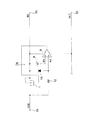
最初に、本発明の実施の形態におけるブートストラップ回路の第1の基本構成例について、図1を参照しつつ説明する。
本発明の実施の形態におけるブートストラップ回路は、電源電圧VDDが印加される動作用電源端子31と出力端子32との間に、動作用電源端子31側から順に直列接続されて設けられたスイッチ素子としての第1のMOSトランジスタ1及びブートストラップキャパシタ5と、第1のMOSトランジスタ1のON/OFFを制御する電流監視回路(図1においては「I−WATCH」と表記)7と、さらに、第1のMOSトランジスタ1と共にブートストラップキャパシタ5の充電を制御する第2及び第3のMOSトランジスタ2,3と、これら第2及び第3のMOSトランジスタ2,3の動作を制御するコントロール回路4とを主たる構成要素として構成されたものとなっている。
Hereinafter, embodiments of the present invention will be described with reference to FIGS. 1 to 4.
The members and arrangements described below do not limit the present invention and can be variously modified within the scope of the gist of the present invention.
First, a first basic configuration example of the bootstrap circuit in the embodiment of the present invention will be described with reference to FIG.
The bootstrap circuit according to the embodiment of the present invention includes a switch element provided in series between the operation
以下、具体的に回路接続について説明する。
まず、Pチャンネルの第1のMOSトランジスタ1は、そのドレインに電源電圧VDDが印加されるようになっている一方、ソースは、ブートストラップキャパシタ5の一端に接続されている。なお、第1のMOSトランジスタ1のソースとブートストラップキャパシタ5の一端との接続点は、ブートストラップ電圧端子(図1においては「BS」と表記)33に接続されている。
そして、ブートストラップキャパシタ5の他端は、出力端子(図1においては「OUT」と表記)32に接続されている。
Hereinafter, the circuit connection will be specifically described.
First, the power supply voltage VDD is applied to the drain of the P-channel first MOS transistor 1, while the source is connected to one end of the
The other end of the
電流監視回路7は、第1のMOSトランジスタ1に流れる電流を監視し、流れる電流に応じて第1のMOSトランジスタ1のゲートに制御信号を出力するよう構成されたものとなっている(詳細は後述)。
一方、第2及び第3のスイッチ素子としてのNチャンネルの第2及び第3のMOSトランジスタ2,3は、第2のMOSトランジスタ2のドレインと第3のMOSトランジスタ3のソースとが接続され、第2のMOSトランジスタ2のソースは、グランド端子(図1においては「GND」と表記)34に接続されたものとなっている。また、第3のMOSトランジスタ3のドレインは入力電圧端子35に接続されている。
The current monitoring circuit 7 is configured to monitor a current flowing through the first MOS transistor 1 and output a control signal to the gate of the first MOS transistor 1 in accordance with the flowing current (for details, see FIG. Later).
On the other hand, the N-channel second and
そして、第2のMOSトランジスタ2のゲートには、コントロール回路(図1においては「CONT」と表記)4から出力されるローサイドゲート信号LG1が印加されるようになっている。
また、第3のMOSトランジスタ3のゲートには、レベルシフタ回路(図1においては「LS」と表記)6から出力されるハイサイドゲート信号HG2が印加されるようになっている。
レベルシフタ回路6は、電源電圧VDDからブーストラップ電圧端子33の電圧VBSに電圧シフトし、コントロール回路4からの制御信号HG1に同期して、ハイサイド信号HG2を出力するよう構成されてなるものである。
A low-side gate signal LG1 output from a control circuit (indicated as “CONT” in FIG. 1) 4 is applied to the gate of the
Further, a high side gate signal HG2 output from a level shifter circuit (indicated as “LS” in FIG. 1) 6 is applied to the gate of the
The
コントロール回路4は、外部から入力されるPWM(Pulse Width Modulation)信号に基づいて、第2のMOSトランジスタ2のゲート信号としての制御信号LG1や、レベルシフタ回路6の制御信号HG1を出力するよう構成されてなるものである。
コントロール回路4は、電源電圧VDDの供給を受けて動作する。
The control circuit 4 is configured to output a control signal LG1 as a gate signal of the
The control circuit 4 operates upon receiving the power supply voltage VDD.
図2には、電流監視回路7の具体回路構成例が示されており、以下、同図を参照しつつ、この具体回路例について説明する。
本発明の実施の形態における電流監視回路7は、監視回路用第1乃至第4のMOSトランジスタ21〜24と、比較器9とを主たる構成要素として構成されてなるものである。
監視回路用第1乃至第4のMOSトランジスタ21〜24には、PチャンネルのMOSトランジスタが用いられており、監視回路用第1及び第2のMOSトランジスタ21,22によりカレントミラー回路が、また、監視回路用第3及び第4のMOSトランジスタ23,24により入力制限回路がそれぞれ構成されて、縦続接続された構成となっている。
FIG. 2 shows a specific circuit configuration example of the current monitoring circuit 7. Hereinafter, this specific circuit example will be described with reference to FIG.
The current monitoring circuit 7 according to the embodiment of the present invention is configured by the monitoring circuit first to
P-channel MOS transistors are used for the first to
すなわち、監視回路用第1及び第2のMOSトランジスタ21,22は、各々のゲートと、監視回路用第2のMOSトランジスタ22のドレインとが相互に接続される一方、監視回路用第1及び第2のMOSトランジスタ21,22のソースはともに接続されたものとなっている。
That is, the first and
一方、監視回路用第3及び第4のMOSトランジスタ23、24は、各々のゲートと、監視回路用第4のMOSトランジスタ24のドレインとが相互に接続される一方、監視回路用第3のMOSトランジスタ23のソースは、監視回路用第1のMOSトランジスタ21のドレインと、また、監視回路用第4のMOSトランジスタ24のソースは、監視回路用第2のMOSトランジスタ22のドレインと、それぞれ接続されたものとなっている。
On the other hand, the third and
そして、監視回路用第3のMOSトランジスタ23のソースは、第1のMOSトランジスタ21のドレインと共に、比較器9の反転入力端子に接続される一方、監視回路用第4のMOSトランジスタ24のドレインと出力端子32との間には、定電流源25が接続されている。
かかる構成において、監視用第1及び第3のMOSトランジスタ21,23は、第1のMOSトランジスタ1に並列接続された電流源11として機能するものとなっている(詳細は後述)。
The source of the
In this configuration, the first and
そして、比較器9の非反転入力端子には、基準電圧VREFが逆極性で印加されるようになっている。すなわち、基準電圧源8は、その負極側が比較器9の非反転入力端子に、正極側がブートストラップ電圧端子33に、それぞれ接続されて設けられたものとなっている。
また、比較器9の出力端子は、第1のMOSトランジスタ1のゲートに接続されたものとなっている。
The reference voltage VREF is applied to the non-inverting input terminal of the
The output terminal of the
次に、かかる構成における動作について説明する。
まず、前提条件として、基準電圧源8の基準電圧VREFは、VBS≧VDDの場合(以下、便宜的に、かかる状態を「状態1」と称する)において、VBS>VN1≧VN2を満たすよう設定されているものとする。
ここで、VBSは、グランド端子34における端子電圧を基準としたブートストラップ電圧端子33における端子電圧であり、VN1は、比較器9の非反転入力端子における電圧で、VN1=VBS−VREFと表すことができるものである。また、VN2は、比較器9の反転入力端子における電圧である。
Next, the operation in this configuration will be described.
First, as a precondition, the reference voltage VREF of the
Here, VBS is the terminal voltage at the
最初に、ブートストラップ回路としての基本的な動作は、第1のMOSトランジスタ1が後述するように電流監視回路7によってON/OFF制御される点を除けば、この種の従来回路と同様であるので、その詳細な説明は省略し、概括的に説明するに留めることとする。
すなわち、ブートストラップ動作は、まず、電流監視回路7により第1のMOSトランジスタ1がON、コントロール回路4により第2のMOSトランジスタ2がON、第3のMOSトランジスタ3がOFFとされることにより、VOUT =VGNDとなり、ブートストラップキャパシタ5が充電され、VBS-OUT≒VDDとなる。
なお、ここで、VOUT は、グランド端子34における端子電圧を基準とした出力端子32における端子電圧、VGNDは、グランド端子34の電圧、VBS-OUTは、出力端子32の端子電圧を基準としたブートストラップ電圧端子33における端子電圧である。
First, the basic operation as a bootstrap circuit is the same as that of this type of conventional circuit except that the first MOS transistor 1 is ON / OFF controlled by a current monitoring circuit 7 as will be described later. Therefore, a detailed description thereof will be omitted, and only a general description will be given.
That is, in the bootstrap operation, first, the first MOS transistor 1 is turned on by the current monitoring circuit 7, the
Here, VOUT is a terminal voltage at the
そして、VBS-OUT≒VDDとなったところで、第1のMOSトランジスタ1OFF、第2のMOSトランジスタ2がOFF、第3のMOSトランジスタ3がONとされ、VOUT=VI Nとなるため、VBS≒VIN+VDDとなる。
なお、ここで、VI Nは、グランド端子34の端子電圧を基準とした入力電圧端子35における電圧であり、この電圧VINは、図示を省略した第2の電源により外部から供給されるものとなっている。
When VBS-OUT≈VDD, the first MOS transistor 1OFF, the
Here, VIN is a voltage at the
次に、電流監視回路7を中心とした動作について、先の前提条件の下、説明することとする。
最初に、回路の動作状態が状態1である場合、すなわち、にVBS≧VDDの状態にある場合、ブートストラップ電圧端子33から第1のMOSトランジスタ1を介して動作用電源端子31へ電流が流れるのを阻止する必要がある。
かかる状態にあって、VN1≧VN2であるため、比較器9からは、論理値Highに相当する信号が出力され、第1のMOSトランジスタ1のゲートに印加されて、第1のMOSトランジスタ1はOFF状態とされる。
そのため、ブートストラップ電圧端子33から動作用電源端子31へ電流が流れることが確実に阻止されることとなる。
Next, the operation centering on the current monitoring circuit 7 will be described under the above preconditions.
First, when the operation state of the circuit is state 1, that is, when VBS ≧ VDD, a current flows from the
In this state, since VN1 ≧ VN2, a signal corresponding to the logical value High is output from the
This reliably prevents current from flowing from the
次に、VDD>VBSの場合(以下、便宜的に、かかる状態を「状態2」と称する)、比較器9の反転入力端子の電圧VN2は、VN2>VN1となるため、比較器9からは、論理値Lowに相当する信号が出力され、第1のMOSトランジスタ1のゲートに印加され、第1のMOSトランジスタ1は、ON状態とされる。それによって、動作用電源端子31とブ−トストラップ電圧端子33が導通状態となり、動作用電源端子31からブートストラップ電圧端子33へ電流が流れ、ブートストラップキャパシタ5の充電が行われることとなる。
このように、第1のMOSトランジスタ1は、流れる電流が電流監視回路7によって監視され、その監視結果に応じて、ON/OFFが自己制御されるようになっている。
Next, when VDD> VBS (hereinafter, for convenience, this state is referred to as “
In this way, the current flowing through the first MOS transistor 1 is monitored by the current monitoring circuit 7, and ON / OFF is self-controlled according to the monitoring result.
次に、第2の構成例について、図3及び図4を参照しつつ説明する。
なお、図1又は図2に示された構成要素と同一の構成要素については、同一の符号を付して、その詳細な説明を省略し、以下、異なる点を中心に説明する。
この第2の構成例は、先の第1の構成例における電流監視回路7に代えて、電圧監視回路(図3においては「V−WATCH」と表記)7Aを設け(図3参照)、それによって、電流監視回路7同様に第1のMOSトランジスタ1のON/OFF制御を可能としたものである。
図4には、電圧監視回路7Aの具体回路構成例が示されており、以下、同図を参照しつつ、電圧監視回路7Aについて説明する。
Next, a second configuration example will be described with reference to FIGS.
The same constituent elements as those shown in FIG. 1 or FIG. 2 are denoted by the same reference numerals, detailed description thereof is omitted, and different points will be mainly described below.
This second configuration example is provided with a voltage monitoring circuit (indicated as “V-WATCH” in FIG. 3) 7A instead of the current monitoring circuit 7 in the first configuration example (see FIG. 3). As in the current monitoring circuit 7, ON / OFF control of the first MOS transistor 1 can be performed.
FIG. 4 shows a specific circuit configuration example of the
電圧監視回路7Aは、第1のMOSトランジスタ1のソース・ドレイン間の電圧を監視し、その監視結果に応じて、第1のMOSトランジスタ1のON/OFF制御を行うよう構成されてなるものである。
かかる本発明の実施の形態における電圧監視回路7Aは、ツェナーダイオード13と、比較器9とを主たる構成要素として構成されてなるものである。
ツェナーダイオード13は、そのアノードが比較器9の反転入力端子に接続されると共に、抵抗器12を介して第1のトランジスタMOS1のドレインに接続されており、回路動作用電源電圧VDDが印加されるようになっている。
The
The
The
一方、ツェナーダイオード13のカソードは、第1のMOSトランジスタ1のソースに接続されている。なお、この構成例において、第1のMOSトランジスタ1は、サブストレートがソースに接続されたものとなっている。
比較器9と基準電圧源8の接続は、先に図2に示された構成例と同一であるので、ここでの再度の詳細な説明は省略することとする。
On the other hand, the cathode of the
Since the connection between the
次に、かかる構成における電圧監視回路7Aの動作について説明する。
この電圧監視回路7Aにおいては、第1のMOSトランジスタ1のソース・ドレイン間の電圧が比較器9により監視されることとなる。すなわち、第1のMOSトランジスタ1のソース・ドレイン間の電圧が、基準電圧源8の基準電圧VREF以上となると、比較器9からは論理値Highに相当する信号が出力され、第1のMOSトランジスタ1がOFFとされる。
ここで、第1のMOSトランジスタ1のソース・ドレイン間の電圧が基準電圧源8の基準電圧VREF以上となり、比較器9により第1のMOSトランジスタ1がOFFとされるのは、ブートストラップキャパシタ5の充電が進行し、VBS-OUT≒VDDとなった時点である。
Next, the operation of the
In the
Here, the voltage between the source and the drain of the first MOS transistor 1 becomes equal to or higher than the reference voltage VREF of the
一方、上述とは逆に、第1のMOSトランジスタ1のソース・ドレイン間の電圧が基準電圧源8の基準電圧VREFを下回ると、比較器9からは論理値Lowに相当する信号が出力され、第1のMOSトランジスタ1がONとされる。
このように、第1のMOSトランジスタ1は、ブートストラップキャパシタ5の電圧の変化に起因するソース・ドレイン間電圧の変化に応じて電圧監視回路7Aによって、そのON/OFFがいわば自己制御されるようになっている。
On the other hand, contrary to the above, when the voltage between the source and drain of the first MOS transistor 1 falls below the reference voltage VREF of the
In this way, the first MOS transistor 1 is self-controlled by the
1…第1のMOSトランジスタ
2…第2のMOSトランジスタ
3…第3のMOSトランジスタ
4…コントロール回路
5…ブートストラップキャパシタ
6…レベルシフタ回路
7…電流監視回路
7A…電圧監視回路
DESCRIPTION OF SYMBOLS 1 ...
Claims (2)
前記第1のスイッチ素子に流れる電流を監視し、その監視結果に応じて、前記第1のスイッチ素子のON、OFFを制御する電流監視回路が設けられ、前記電流監視回路は、監視回路用第1乃至第4のMOSトランジスタと、比較器を有し、前記監視回路用第1及び第2のMOSトランジスタは、各々のゲートと、前記監視回路用第2のMOSトランジスタのドレインとが相互に接続される一方、前記監視回路用第1及び第2のMOSトランジスタのソースは共に、前記第1のスイッチ素子としての第1のMOSトランジスタのソースと前記ブートストラップキャパシタの一端に接続され、前記監視回路用第3及び第4のMOSトランジスタは、各々のゲートと、前記監視回路用第4のMOSトランジスタのドレインとが相互に接続される一方、前記監視回路用第3のMOSトランジスタのソースは、前記監視回路用第1のMOSトランジスタのドレインと、また、前記監視回路用第4のMOSトランジスタのソースは、前記監視回路用第2のトランジスタのドレインと、それぞれ接続され、前記監視回路用第3のMOSトランジスタのソースは、前記監視回路用第1のMOSトランジスタのドレインと共に、前記比較器の反転入力端子に接続され、前記監視回路用第3のMOSトランジスタのドレインは、前記第1の電源に接続され、前記監視回路用第4のMOSトランジスタのドレインと出力端子との間には、定電流源が接続され、前記比較器の非反転入力端子には、基準電圧源の負極側が接続され、前記基準電圧源の正極側が前記第1のスイッチ素子としての第1のMOSトランジスタのソースに接続され、前記比較器の出力端子は、前記第1のスイッチ素子としての第1のMOSトランジスタのゲートに接続されてなり、前記ブートストラップ電圧が前記第1の電源の電源電圧を超えた状態にある場合に、前記比較器の非反転入力端子の電圧が前記比較器の反転入力端子の電圧を超えて、前記比較器により論理値Highに相当する信号が出力され、前記第1のスイッチ素子としての第1のMOSトランジスタがOFF状態とされる一方、前記ブートストラップ電圧が前記第1の電源の電源電圧を下回る場合に、前記比較器の反転入力端子の電圧が前記比較器の非反転入力端子の電圧を超えて、前記比較器により論理値Lowに相当する信号が出力され、前記第1のスイッチ素子としての第1のMOSトランジスタがON状態とされるよう構成されてなることを特徴とするブートストラップ回路。 A first switch element and a bootstrap capacitor are connected in series between the first power source and the output terminal, while a second switch element is connected between the output terminal and the first terminal between the output terminal and the ground terminal. A third switch element is connected in series with the two power supplies, and the boot switch capacitor is booted to the first switch element side terminal by controlling the operation of the first to third switch elements. In a bootstrap circuit configured to obtain a strap voltage,
A current monitoring circuit that monitors the current flowing through the first switch element and controls ON / OFF of the first switch element according to the monitoring result is provided . 1 to 4 MOS transistors and a comparator, and the first and second MOS transistors for the monitoring circuit are connected to each other and the drain of the second MOS transistor for the monitoring circuit. On the other hand, the sources of the first and second MOS transistors for the monitoring circuit are both connected to the source of the first MOS transistor as the first switch element and one end of the bootstrap capacitor, In the third and fourth MOS transistors, the gate and the drain of the fourth MOS transistor for monitoring circuit are connected to each other. The source of the third MOS transistor for the monitoring circuit is the drain of the first MOS transistor for the monitoring circuit, and the source of the fourth MOS transistor for the monitoring circuit is the second transistor for the monitoring circuit And the source of the third MOS transistor for the monitoring circuit is connected to the inverting input terminal of the comparator together with the drain of the first MOS transistor for the monitoring circuit. The drain of the third MOS transistor is connected to the first power supply, a constant current source is connected between the drain of the fourth MOS transistor for monitoring circuit and the output terminal, and the non-inversion of the comparator The input terminal is connected to the negative side of the reference voltage source, and the positive side of the reference voltage source is a first MOS transistor as the first switch element. And the output terminal of the comparator is connected to the gate of a first MOS transistor as the first switch element, and the bootstrap voltage is the power supply voltage of the first power supply. When the voltage exceeds the voltage at the non-inverting input terminal of the comparator exceeding the voltage at the inverting input terminal of the comparator, a signal corresponding to the logical value High is output by the comparator. When the first MOS transistor as the switch element is turned off while the bootstrap voltage is lower than the power supply voltage of the first power supply, the voltage at the inverting input terminal of the comparator is A signal corresponding to the logical value Low is output by the comparator beyond the voltage at the non-inverting input terminal, and the first MOS transistor as the first switch element A bootstrap circuit configured to be turned on .
前記第1のスイッチ素子の端子間の電圧を監視し、その監視結果に応じて、前記第1のスイッチ素子のON、OFFを制御する電圧監視回路が設けられ、前記電圧監視回路は、ツェナーダイオードと比較器を有し、前記ツェナーダイオードは、そのアノードが前記比較器の反転入力端子に接続されると共に、抵抗器を介して前記第1のスイッチ素子としての第1のMOSトランジスタのドレインに接続される一方、前記ツェナーダイオードのカソードは、前記ブートストラップキャパシタに接続される前記第1のスイッチ素子としての第1のMOSトランジスタのソースに接続され、前記比較器の非反入力端子は、基準電圧源の負極側に接続され、前記基準電圧源の正極側は前記第1のスイッチ素子としての第1のMOSトランジスタのソースに接続され、前記比較器の出力端子は、前記第1のスイッチ素子としての第1のMOSトランジスタのゲートに接続されてなり、前記第1のスイッチ素子としての第1のMOSトランジスタのソース・ドレイン間の電圧が、前記基準電圧源の基準電圧以上となった際に、前記比較器により論理値Highに相当する電圧が出力され、前記第1のスイッチ素子としての第1のMOSトランジスタがOFF状態とされる一方、前記第1のスイッチ素子としての第1のMOSトランジスタのソース・ドレイン間の電圧が、前記基準電圧源の基準電圧を下回った際に、前記比較器により論理値Lowに相当する電圧が出力され、前記第1のスイッチ素子としての第1のMOSトランジスタがON状態とされるよう構成されてなることを特徴とするブートストラップ回路。 A first switch element and a bootstrap capacitor are connected in series between the first power source and the output terminal, while a second switch element is connected between the output terminal and the first terminal between the output terminal and the ground terminal. A third switch element is connected in series with the two power supplies, and the boot switch capacitor is booted to the first switch element side terminal by controlling the operation of the first to third switch elements. In a bootstrap circuit configured to obtain a strap voltage,
A voltage monitoring circuit that monitors the voltage between the terminals of the first switch element and controls ON / OFF of the first switch element according to the monitoring result is provided, and the voltage monitoring circuit includes a Zener diode The Zener diode has an anode connected to the inverting input terminal of the comparator and a drain connected to the drain of the first MOS transistor as the first switch element. Meanwhile, the cathode of the Zener diode is connected to the source of the first MOS transistor as the first switch element connected to the bootstrap capacitor, and the non-reverse input terminal of the comparator is connected to a reference voltage Connected to the negative side of the source, the positive side of the reference voltage source is the source of the first MOS transistor as the first switch element. And the output terminal of the comparator is connected to the gate of the first MOS transistor as the first switch element, and the source / drain of the first MOS transistor as the first switch element When the voltage between them becomes equal to or higher than the reference voltage of the reference voltage source, the comparator outputs a voltage corresponding to the logical value High, and the first MOS transistor as the first switch element is in the OFF state. On the other hand, when the voltage between the source and the drain of the first MOS transistor as the first switch element falls below the reference voltage of the reference voltage source, the comparator corresponds to the logical value Low. voltage is output, the blanking of the first MOS transistor as a first switch element is characterized by comprising is configured to be turned ON Bootstrap circuit.
Priority Applications (1)
| Application Number | Priority Date | Filing Date | Title |
|---|---|---|---|
| JP2008293966A JP5248993B2 (en) | 2008-11-18 | 2008-11-18 | Bootstrap circuit |
Applications Claiming Priority (1)
| Application Number | Priority Date | Filing Date | Title |
|---|---|---|---|
| JP2008293966A JP5248993B2 (en) | 2008-11-18 | 2008-11-18 | Bootstrap circuit |
Publications (2)
| Publication Number | Publication Date |
|---|---|
| JP2010124083A JP2010124083A (en) | 2010-06-03 |
| JP5248993B2 true JP5248993B2 (en) | 2013-07-31 |
Family
ID=42325047
Family Applications (1)
| Application Number | Title | Priority Date | Filing Date |
|---|---|---|---|
| JP2008293966A Expired - Fee Related JP5248993B2 (en) | 2008-11-18 | 2008-11-18 | Bootstrap circuit |
Country Status (1)
| Country | Link |
|---|---|
| JP (1) | JP5248993B2 (en) |
Families Citing this family (4)
| Publication number | Priority date | Publication date | Assignee | Title |
|---|---|---|---|---|
| JP6113489B2 (en) * | 2012-12-14 | 2017-04-12 | ラピスセミコンダクタ株式会社 | Semiconductor circuit and semiconductor device |
| US10079538B2 (en) * | 2016-10-18 | 2018-09-18 | Texas Instruments Incorporated | Bootstrap circuit for DC/DC converter |
| CN109995235B (en) * | 2019-04-30 | 2024-03-08 | 广东美的制冷设备有限公司 | Intelligent power module and electrical equipment |
| CN114946124A (en) * | 2020-01-14 | 2022-08-26 | 罗姆股份有限公司 | Semiconductor device with a plurality of semiconductor chips |
Family Cites Families (4)
| Publication number | Priority date | Publication date | Assignee | Title |
|---|---|---|---|---|
| US5761020A (en) * | 1996-01-29 | 1998-06-02 | International Rectifier Corporation | Fast switching smartfet |
| JP3682226B2 (en) * | 2000-12-22 | 2005-08-10 | 株式会社オートネットワーク技術研究所 | Disconnection detection circuit |
| JP4896522B2 (en) * | 2006-01-05 | 2012-03-14 | 株式会社日立製作所 | Switch circuit and railway signal interlocking control system |
| JP4830507B2 (en) * | 2006-01-20 | 2011-12-07 | 富士電機株式会社 | Bootstrap circuit |
-
2008
- 2008-11-18 JP JP2008293966A patent/JP5248993B2/en not_active Expired - Fee Related
Also Published As
| Publication number | Publication date |
|---|---|
| JP2010124083A (en) | 2010-06-03 |
Similar Documents
| Publication | Publication Date | Title |
|---|---|---|
| US9621156B2 (en) | Analog switches and methods for controlling analog switches | |
| US7274226B2 (en) | Power source voltage monitoring circuit for self-monitoring its power source voltage | |
| JP5220240B2 (en) | Coupling circuit, driver circuit including the coupling circuit, and control method of the coupling circuit | |
| US10454376B1 (en) | Power supply circuit | |
| US20120068740A1 (en) | Voltage output circut | |
| JP4618164B2 (en) | Switch circuit | |
| US6661260B2 (en) | Output circuit of semiconductor circuit with power consumption reduced | |
| US11105830B2 (en) | Voltage detector | |
| US6977523B2 (en) | Voltage level shifting circuit | |
| JP5248993B2 (en) | Bootstrap circuit | |
| US20150270774A1 (en) | Power supply circuit | |
| US7893752B2 (en) | Charge pump circuit with control circuitry | |
| US20170117888A1 (en) | Voltage comparison circuit | |
| US20180159526A1 (en) | Switching element driving device | |
| US7514960B2 (en) | Level shifter circuit | |
| JP2010028522A (en) | Semiconductor device | |
| WO2017195427A1 (en) | Power supply device and electronic control device | |
| US10205446B2 (en) | Semiconductor device | |
| JP2010021818A (en) | Multifunctional driver circuit | |
| US20200067501A1 (en) | Switch circuitry | |
| JP2021087233A (en) | Short-circuiting determination device | |
| JP4594064B2 (en) | Surge current suppression circuit and DC power supply device | |
| WO2012137670A1 (en) | Load current detection circuit | |
| JP4307314B2 (en) | Load drive circuit | |
| US20230421153A1 (en) | Semiconductor integrated circuit |
Legal Events
| Date | Code | Title | Description |
|---|---|---|---|
| A621 | Written request for application examination |
Free format text: JAPANESE INTERMEDIATE CODE: A621 Effective date: 20110930 |
|
| A977 | Report on retrieval |
Free format text: JAPANESE INTERMEDIATE CODE: A971007 Effective date: 20121031 |
|
| A131 | Notification of reasons for refusal |
Free format text: JAPANESE INTERMEDIATE CODE: A131 Effective date: 20121218 |
|
| A521 | Request for written amendment filed |
Free format text: JAPANESE INTERMEDIATE CODE: A523 Effective date: 20130215 |
|
| TRDD | Decision of grant or rejection written | ||
| A01 | Written decision to grant a patent or to grant a registration (utility model) |
Free format text: JAPANESE INTERMEDIATE CODE: A01 Effective date: 20130402 |
|
| A61 | First payment of annual fees (during grant procedure) |
Free format text: JAPANESE INTERMEDIATE CODE: A61 Effective date: 20130411 |
|
| R150 | Certificate of patent or registration of utility model |
Ref document number: 5248993 Country of ref document: JP Free format text: JAPANESE INTERMEDIATE CODE: R150 Free format text: JAPANESE INTERMEDIATE CODE: R150 |
|
| FPAY | Renewal fee payment (event date is renewal date of database) |
Free format text: PAYMENT UNTIL: 20160419 Year of fee payment: 3 |
|
| R250 | Receipt of annual fees |
Free format text: JAPANESE INTERMEDIATE CODE: R250 |
|
| R250 | Receipt of annual fees |
Free format text: JAPANESE INTERMEDIATE CODE: R250 |
|
| R250 | Receipt of annual fees |
Free format text: JAPANESE INTERMEDIATE CODE: R250 |
|
| R250 | Receipt of annual fees |
Free format text: JAPANESE INTERMEDIATE CODE: R250 |
|
| LAPS | Cancellation because of no payment of annual fees |