JP5245004B2 - Low power memory hierarchy for high performance video processors - Google Patents
Low power memory hierarchy for high performance video processors Download PDFInfo
- Publication number
- JP5245004B2 JP5245004B2 JP2012273316A JP2012273316A JP5245004B2 JP 5245004 B2 JP5245004 B2 JP 5245004B2 JP 2012273316 A JP2012273316 A JP 2012273316A JP 2012273316 A JP2012273316 A JP 2012273316A JP 5245004 B2 JP5245004 B2 JP 5245004B2
- Authority
- JP
- Japan
- Prior art keywords
- buffer
- memory
- client
- transfer
- external
- Prior art date
- Legal status (The legal status is an assumption and is not a legal conclusion. Google has not performed a legal analysis and makes no representation as to the accuracy of the status listed.)
- Active
Links
- 230000015654 memory Effects 0.000 title claims description 107
- 239000000872 buffer Substances 0.000 claims description 94
- 230000033001 locomotion Effects 0.000 claims description 54
- 239000013598 vector Substances 0.000 claims description 20
- 238000000034 method Methods 0.000 claims description 10
- 238000012432 intermediate storage Methods 0.000 claims 1
- 230000004044 response Effects 0.000 claims 1
- 238000010586 diagram Methods 0.000 description 8
- 230000006835 compression Effects 0.000 description 3
- 238000007906 compression Methods 0.000 description 3
- 238000005516 engineering process Methods 0.000 description 2
- 238000013139 quantization Methods 0.000 description 2
- 230000009466 transformation Effects 0.000 description 2
- 230000000007 visual effect Effects 0.000 description 2
- 238000003491 array Methods 0.000 description 1
- 230000006399 behavior Effects 0.000 description 1
- 230000005540 biological transmission Effects 0.000 description 1
- 230000003139 buffering effect Effects 0.000 description 1
- 230000006837 decompression Effects 0.000 description 1
- 230000000694 effects Effects 0.000 description 1
- 238000005562 fading Methods 0.000 description 1
- 238000001914 filtration Methods 0.000 description 1
- 230000007774 longterm Effects 0.000 description 1
- 230000008520 organization Effects 0.000 description 1
- 230000003068 static effect Effects 0.000 description 1
- 239000002699 waste material Substances 0.000 description 1
Images


Classifications
-
- H—ELECTRICITY
- H04—ELECTRIC COMMUNICATION TECHNIQUE
- H04N—PICTORIAL COMMUNICATION, e.g. TELEVISION
- H04N19/00—Methods or arrangements for coding, decoding, compressing or decompressing digital video signals
- H04N19/42—Methods or arrangements for coding, decoding, compressing or decompressing digital video signals characterised by implementation details or hardware specially adapted for video compression or decompression, e.g. dedicated software implementation
- H04N19/43—Hardware specially adapted for motion estimation or compensation
- H04N19/433—Hardware specially adapted for motion estimation or compensation characterised by techniques for memory access
-
- H—ELECTRICITY
- H04—ELECTRIC COMMUNICATION TECHNIQUE
- H04N—PICTORIAL COMMUNICATION, e.g. TELEVISION
- H04N19/00—Methods or arrangements for coding, decoding, compressing or decompressing digital video signals
- H04N19/60—Methods or arrangements for coding, decoding, compressing or decompressing digital video signals using transform coding
- H04N19/61—Methods or arrangements for coding, decoding, compressing or decompressing digital video signals using transform coding in combination with predictive coding
Landscapes
- Engineering & Computer Science (AREA)
- Multimedia (AREA)
- Signal Processing (AREA)
- Compression Or Coding Systems Of Tv Signals (AREA)
- Picture Signal Circuits (AREA)
- Image Input (AREA)
- Dram (AREA)
Description
本発明は一般的にはメモリに関し、特には高性能ビデオプロセッサ用の低電力メモリ階層を実現するための方法及び/又はアーキテクチャに関する。 The present invention relates generally to memory, and more particularly to a method and / or architecture for implementing a low power memory hierarchy for high performance video processors.
従来の高い帯域幅(伝送容量)のメモリシステムはリアルタイム(実時間)ビデオ符号化(エンコーディング)のような要求の厳しい画像処理アプリケーションに使用される。フレーム落ちは許されないので、想定される最悪の場合のメモリの待ち時間と帯域幅はビデオ符号化システム基準を満足しなければならない。H.264標準のような、最近のビデオ符号化や高効率符号化システムは想定される最悪の場合の帯域幅の仕様を大幅に高めている。従来のリアルタイムシステムにおいては、外部のダイナミック・アクセス・メモリ(DRAM)チップが、リアルタイムビデオ符号化の際、想定される最悪の場合でも十分な帯域幅を提供している。 Conventional high bandwidth (transmission capacity) memory systems are used in demanding image processing applications such as real-time video coding. Since frame dropping is not allowed, the worst case memory latency and bandwidth expected must meet video coding system standards. H. Modern video coding and high-efficiency coding systems, such as the H.264 standard, have greatly increased the worst-case bandwidth specification envisaged. In conventional real-time systems, an external dynamic access memory (DRAM) chip provides sufficient bandwidth for real-time video encoding, even in the worst case scenario.
しかしながら、従来のオンチップ・キャッシュは、キャッシュをヒットした場合には十分な帯域幅と待ち時間を提供し、キャッシュをヒットしなかった場合には想定される最悪の場合での十分な性能を提供しない。この結果、最新のリアルタイムビデオ処理回路の電力消費は携帯用アプリケーションには余りに大き過ぎる。 However, traditional on-chip caches provide sufficient bandwidth and latency if the cache is hit, and provide the worst-case performance expected if the cache is not hit. do not do. As a result, the power consumption of modern real-time video processing circuits is too great for portable applications.
本発明は、一般的に内部メモリと外部転送回路とを備える装置に関する。内部メモリはチップ上に配置されるとともに(i)動き補償に適し(ii)チップ外の外部メモリに格納された少なくとも1つの基準フレームのサブセットを格納するための少なくとも1つの第1のバッファを含む。前記少なくとも1つの第1のバッファの大きさは通常、基準フレーム内のブロックの1行より大きい。外部転送回路はチップ上に配置され、サブセットを外部メモリから内部メモリへ転送するように構成される。 The present invention generally relates to an apparatus including an internal memory and an external transfer circuit. The internal memory is disposed on the chip and includes (i) suitable for motion compensation (ii) at least one first buffer for storing a subset of at least one reference frame stored in external memory outside the chip. . The at least one first buffer is typically larger than one row of blocks in the reference frame. The external transfer circuit is disposed on the chip and is configured to transfer the subset from the external memory to the internal memory.
本発明の目的、特徴、及び利点としては、(i)消費電力を低減し、(ii)外部メモリに対する使用帯域幅を最小化し、(iii)外部メモリへアクセスする待ち時間を見えないようにし、及び/又は(iv)外部メモリとの効率的な長時間バースト交換を最大化することができる高性能ビデオプロセッサ用のメモリ階層を提供することにある。 Objects, features, and advantages of the present invention include: (i) reducing power consumption, (ii) minimizing bandwidth used for external memory, and (iii) invisible latency to access external memory, And / or (iv) to provide a memory hierarchy for a high performance video processor capable of maximizing efficient long burst exchange with external memory.
本発明のこれら及び他の目的、機能と利点は、以下の詳細な説明と添付の特許請求の範囲と図面から明白になる。 These and other objects, features and advantages of the present invention will become apparent from the following detailed description and the appended claims and drawings.
本発明によれば、(i)消費電力を低減し、(ii)外部メモリに対する使用帯域幅を最小化し、(iii)外部メモリへアクセスする待ち時間を見えないようにし、及び/又は(iv)外部メモリとの効率的な長時間バースト交換を最大化することができる。 In accordance with the present invention, (i) reduce power consumption, (ii) minimize the bandwidth used for external memory, (iii) hide the latency to access external memory, and / or (iv) Efficient long-term burst exchange with external memory can be maximized.
図1を参照すると、本発明の好適な一実施形態によるシステム100のブロック図が示されている。システム(又は装置)100は通常、回路(又はチップ)102と回路(又はチップ)104とを含む。回路102のインタフェース106は回路104のインタフェース108へ接続される。信号(例えばEXT)は、インタフェース106、108を介して回路102と回路104間で転送される。回路102は入力信号(例えばVIDEO_IN)を受信することができる。出力信号(例えばVIDEO_OUT)は回路102から送信される。
Referring to FIG. 1, a block diagram of a
回路102はビデオチップと称されるものである。ビデオチップ102は、回路104内に格納されたビデオ情報を処理するように動作可能である。限定するものではないが、この処理は符号化、復号化、動き予測、及び動き補償を含む。ビデオチップ102は通常、単一の集積回路ダイすなわちチップとして作製される。ビデオ情報の一部は、信号EXTにより回路104から処理用のビデオチップ102へ搬送される。ビデオ情報もまた信号EXTによりビデオチップ102から回路104へ搬送され、戻される。
The
回路104は外部メモリ・チップと称されるものである。外部メモリ・チップ104は通常、単一の集積回路ダイ又はチップとしてビデオチップ102とは別に作製される。外部メモリ・チップ104は、1つ又は2以上の基準フレームと、1つ又は2以上の処理すべきフレームと、1つ又は2以上の処理されたフレームとを含む多数のビデオフレームを格納するように動作可能である。
The
符号化の実施形態に関し、ビデオチップ102により提供される出力ビット・ストリーム(例えば信号VIDEO_OUT)は、(非特許文献1)のビデオ標準ITU-T Revised Recommendationに準拠してよい。復号化の実施形態において、ビデオチップ102により受信された入力ビット・ストリーム(例えば信号VIDEO_IN)は、(非特許文献1)に準拠してよい。特定のアプリケーションの基準を満たすためには他の符号化(コーディング)方法を実施してもよい。
With respect to the encoding embodiment, the output bit stream (eg, signal VIDEO_OUT) provided by the
ビデオチップ102は通常、回路(又はモジュール)110、回路(又はモジュール)112、任意の回路(又はモジュール)114、任意の回路(又はモジュール)116、任意の回路(又はモジュール)118を含む。回路110は信号EXTを通じて外部メモリ・チップ104と通信可能である。信号(例えばINT)は回路110と回路112間でビデオ情報を交換するために使用される。別の信号(例えばBUF)も回路110と回路112間でビデオ情報を交換するために使用される。回路110は信号(例えばCLIENT)内のビデオ情報を、回路114−118と交換することができる。信号(例えばTRANS)は回路114−118により提供され、回路110へ戻される。
The
回路110はダイレクトメモリアクセス(DMA)ユニットと称されるものである。DMAユニット110は、回路112と、外部メモリ・チップ104及び回路114−118の両方との間でデータ(例えば、ビデオフレーム、動きベクトル及び/又はその他ビデオ情報の一部)を転送するように動作可能である。転送制御は、回路114−118からの信号TRANSにおいて受信された情報により管理される。DMAユニット110もまた、転送回路(又はモジュール)と称される。
回路112は、共有メモリ(SMEM:shared memory)回路と称されるものである。SMEM回路112は、外部メモリ・チップ104と回路114−118間で流れるビデオ情報を格納又はバッファするように動作可能なメモリ回路として実装される。SMEM回路112はまた、回路114−118間で転送されたビデオ情報をバッファするように動作可能である。SMEM回路112は通常、DMAユニット110及び回路114−118と同じチップ上に(又は、チップ内に)作製される。
The
回路114は、動き予測(ME)エンジンと称されるものである。MEエンジンは、SMEM回路112とDMAユニット110を介して外部メモリ・チップ104から受信された基準フレーム(参照フレーム)の一部を使用することにより動き予測を行うように実装される。MEエンジン114は、ビデオチップ102がビデオ符号化システムの一部である場合に実施され、ビデオチップ102がビデオ復号化のみのシステムの一部である場合は無くてよい。MEエンジン114は通常、DMAユニット110、SMEM回路112、回路116−118と同一チップ上に(又は、同一チップ内に)作製される。
回路116はクライアント・エンジンと称されるものである。クライアント・エンジン116は、ビデオ情報を処理するためのSMEM回路112にアクセスするように動作可能である。信号VIDEO_INの入力データは、クライアント指定の処理を行うクライアント・エンジン116へルーティングされることができる。出力データはクライアント・エンジン116により生成され、信号VIDEO_OUTに提供される。他のSMEMクライアント(例えば動き予測エンジン114と回路118)は、信号VIDEO_INから入力データを受信し、及び/又は信号VIDEO_OUTに提供される出力データを生成する。クライアント・エンジン116は通常、DMAユニット110、SMEM回路112、MEエンジン114、回路118と同一チップ上に(又は、同一チップ内に)作製される。
回路118は処理エンジンと称されるものである。処理エンジン118はSMEM回路112内にバッファされたビデオ情報を修正するように動作可能である。限定するものではないが、処理エンジン118により行われるビデオ符号化と復号化処理はフォーワード変換及び逆変換、フォーワード量子化及び逆量子化、可変長符号化及び可変長復号化を含むことができる。処理エンジン118は通常、DMAユニット110、SMEM回路112、クライアント・エンジン114、MEエンジン116と同一のチップ上に(又は、同一チップ内に)作製される。
付加的な画像処理動作を行うために、ビデオチップ102には、追加の処理エンジン(図示せず)があってもよい。限定するものではないが、追加の画像処理動作としては色の間引きと補間、コントラスト調整、輝度調整、フェーディング効果、オーバレイ、雑音フィルタリング等が挙げられる。
To perform additional image processing operations,
動き補償は、専用の動き補償エンジンを持たないビデオチップ102により行われる。整数(画素)動き補償はDMAユニット110を使用して行われる。分数(画素)動き補償は、必要に応じSMEMクライアント(例えばクライアント・エンジン116及び/又は処理エンジン118)により行われる。
Motion compensation is performed by the
オンチップのSMEM回路112は通常、処理エンジン114−118により使用される1つ又は2以上の画像フレームのそれぞれを保持するかバッファするために使用される。2つの異なるバッファ・タイプはSMEM回路112に設けられる。第1のバッファ・タイプ120はウインドウ・バッファと称されるものである。SMEM回路112内では、1つ又は2以上のウインドウ・バッファ120が同時に存在することができる。各ウインドウ・バッファ120は、画像(又はフレーム)の全幅と、画像(又はフレーム)の全高さの一部を保持する。例えば、ウインドウ・バッファ120の幅はフレームの幅と一致してもよく、一方、ウインドウ・バッファ120の高さは、フレームの2つ以上のマクロ・ブロック行を格納することができる。
On-
第2のバッファ・タイプ122は小バッファと称されるものである。SMEM回路112内には、ゼロ個又は1個以上の小バッファ122が同時に存在することができる。各小バッファ122の大きさは通常、画像(又はフレーム)の幅及び高さのサブセットである。例えば、小バッファ122は、外部メモリ・チップ104内に格納されたフレームからコピーされたか、あるいはウインドウ・バッファ120からコピーされた単一行のマクロ・ブロックの一部を保持するような大きさである。
The
ウインドウ・バッファ120と小バッファ122は、DMAユニット110内のDMAモジュール124、126と通信することができる。通常、1つ又は2以上の外部DMAモジュール124(図では1つ)、及び1つ又は2以上クライアントDMAモジュール126(図では1つ)は、外部メモリ・チップ104とバッファ120及び/又は122間の転送に、バッファ120及び/又は122と内部処理エンジン114−118間の転送をオーバーラップさせることができる。DMAモジュール124もまた、外部DMA回路(又はチャネル)及び外部転送回路(又はチャネル)と称されるものである。DMAモジュール126もまた、クライアントDMA回路(又はチャネル)及びクライアント転送回路(又はチャネル)と称されるものである。転送回路124、126はハードウェア及び/又はソフトウェアで実現される。DMA回路として以外の、外部転送回路124及び/又はクライアント転送回路126の設計は特定アプリケーションの基準を満たすように実装される。
The
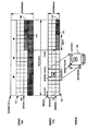
図2を参照すると、ウインドウ・モードにおける画像140の一部のブロック図が示されている。画像(又はフレーム)140は入力されたビデオフレーム又は基準フレームである。画像140は、外部メモリ・チップ104内のある位置(例えばDBASETOP)で始まる位置に配置される。画像140は、ある幅(例えばSCOLMAX)と高さ(例えばDROWMAX)を有する。図2は一般的には、既にSMEM回路112へ転送された画像140の第1の部分142を示す。また、外部メモリ・チップ104からSMEM回路112への画像140の第2の部分144(例えば、1マクロ・ブロック行 × SBLKマクロ・ブロック列)に対して進行中のDMA転送も例示されている。前記の第2の部分144は、画像140の特定行(例えばDROW)と特定列(例えばDCOL)で始まる。画像140の第3の部分146は第2の部分144が転送された後、SMEM回路112へ転送されるようにスケジュールされる。
Referring to FIG. 2, a block diagram of a portion of
送信先ウインドウ・バッファ120は、SMEM回路112内のベース位置(例えばSBASE)で始めると定義される。送信先ウインドウ・バッファ120は、画像140から、画像140のマクロ・ブロック幅SCOLMAXと、いくつかの行(例えばSROWMAX)のブロックとを同時に収容することができる。通常、画像140の幅はウインドウ・バッファ120の幅と一致するので、第2の部分144の始まる列(例えばDCOL)は、ウインドウ・バッファ120と外部メモリ・チップ104では同じである。
The
ウインドウ・バッファ120は、ターゲット・ブロック(マクロ・ブロック)148の垂直方向に制限されたオフセット内の画像140の領域へのランダム・アクセスを援助するように動作する。ターゲット・ブロック148は、ウインドウ・バッファ120内で、ベース位置SBASEに対するある位置(例えば(SROW、SCOL))を有する。
The
ウインドウ・バッファ120は、動き補償されるビデオ圧縮処理に対し特に有用である。通常、ウインドウ・バッファ120の垂直動きベクトル範囲を、動き予測処理の垂直探索範囲に制限される。特に、動きベクトルが余りに大きくなると、関連する動き補償予測値は一般的に不正確となり、また動き予測演算(に使用する演算装置)が余りにも高価なものとなりうる。従って、動き補償に有用な画像140の量は、ターゲット・ブロック148の周りの垂直方向及び水平方向に限定されることとなる。人間の視覚システムは一般的に高速の上下動より高速の水平動を容易に追跡するので、ビデオシーケンスは通常、水平動ベクトル範囲より小さな垂直動きベクトル範囲を有する。その結果、垂直探索範囲は水平探索範囲より小さくでき、限られた数のマクロ・ブロック行のみをウインドウ・バッファ120によりバッファすればよい。
一実施態様においては、オンチップSMEMメモリ回路112は、高速のビデオシーケンスに対する適切な垂直動きベクトル範囲を可能にする組み込み型DRAMあるいは、1トランジスタ・スタティック・ランダムアクセス・メモリ(SRAM)(6トランジスタSRAMではなく)のような高密度オンチップ・メモリ技術を使用することにより実現できる。ウインドウ・バッファ120の垂直範囲は通常、垂直動きベクトル範囲に設定される。通常、垂直ウインドウ・バッファ120の範囲を垂直動きベクトル範囲に一致させることにより、すべての動き予測及び動き補償フェッチは外部メモリ・チップ104においてではなくSMEM回路112のみを使用することにより実行することができる。オンチップSMEM回路112は非常に小さくかつ、処理エンジン114−118により接近しているので、オンチップSMEM回路112へのアクセスは、繰り返し外部メモリ・チップ104へのアクセスするよりはるかに電力効率がよい。更に、オンチップSMEM回路112は通常、小規模な転送へアクセスする際、外部メモリ・チップ104に使用される長いバースト転送用に最適化可能な標準DRAM部品よりはるかに効率的である。
In one embodiment, the on-chip
通常、基準フレーム全体はSMEM回路112内に格納されないので、ターゲット・ブロック148が進められるにつれて(通常はマクロ・ブロックからマクロ・ブロックへ)、外部DMAモジュール124は、新しい基準データをウインドウ・バッファ120へ読み込むとともにウインドウ・バッファ内の最も古いデータを廃棄するように使用される。外部DMAモジュール124はウインドウ・バッファ120を、ターゲット・ブロック148の位置を中心として保持し、その結果、一定の上下動補償範囲が維持される。外部DMAモジュール124は、動き探索の数及び/又は動き補償の数(実行回数)とは無関係に、外部メモリ・チップ104からの基準フレームの各画素をフレーム当たり1回だけロードすることができる。この一回だけのロードは、(i)外部メモリ・チップ104からすべてのデータにアクセスすること、又は(ii)従来のキャッシュ・システムの想定される最悪の場合の動作(より高い待ち時間とキャッシュ・ブロック・サイズのオーバヘッドのせいで外部メモリ・チップ104に直接アクセスすることよりも更に悪い場合)と比較すると、外部メモリ・チップ104とビデオチップ102間の帯域幅を著しく低減することができる。ターゲット・ブロック148を中心とした画像の水平方向に制限された領域を格納する従来のオンチップ・キャッシュでも、ターゲット・ブロック148がマクロ・ブロックの1つの行から次の行へ移動するにつれて、結局、外部メモリ・チップ104からの画像データを複数回読み取り、探索領域の大きさが増加するにつれ、外部メモリ・チップ104の帯域幅の使用を増大することになる。
Normally, the entire reference frame is not stored in the
画像140の一部分が一旦ウインドウ・バッファ120にコピーされると、クライアントDMAモジュール126は、画像140の下位部分(又はサブウインドウ)150をウインドウ・バッファ120から1又は2以上の処理エンジン114−118へ移動することができる。例えば、クライアントDMAモジュール126は、下位部分150を処理エンジン114−118内の1つ又は2以上のローカルメモリ152a−152nへ転送することができる。ローカルメモリ152a−152nは、RMEM(基準メモリ)、TMEM(ターゲットメモリ)、及びローカルメモリ152と略して称する。TMEMは、1つ又は2以上のターゲット・ブロック148を格納する大きさである。RMEMは、1つ又は2以上の基準フレームのターゲット・ブロック148の位置の周りの探索範囲を格納する大きさである。
Once a portion of the
下位部分150は、ターゲット・ブロック148より大きな幅(例えばSCOLCNT)及び高さ(例えばSROWCNT)を有する。通常、動きゼロに対応する基準ブロックは送信先ローカルメモリ152のベース位置(例えばSDESADDR)からオフセット(例えば(YOFFSET、XOFFSET)した下位部分150を中心とする。処理エンジン114−118がターゲット・ブロックに対する動作を完了すると、ターゲットの水平オフセット(例えばSCOL)は、通常はブロックの幅であるプログラム可能な数(例えばCOLINC)だけインクリメント(増加)される。処理エンジン114−118がプログラム可能な数(例えばSCNT)のターゲット・ブロック148に対する動作を完了した後、外部DMAモジュール124は新しい下位部分をウインドウ・バッファ120内にコピーする。ターゲット・ブロック148が一旦ウインドウ・バッファ120内の画像140の端(例えば右側)に到達すると、クライアントDMAモジュール126は、ターゲット(例えばSCOL)の水平オフセットをゼロにリセットし、通常はターゲット高さであるプログラム可能な数(例えばROWINC)だけ垂直オフセットをインクリメントする。
The
図3を参照すると、動きベクトルを有するウインドウ・モードにおける画像140のブロック図が示されている。動き補償処理では、各ターゲット・ブロック148は、1つ又は2以上の基準フレームに対して1つ又は2以上の関連する動きベクトルをそれぞれ有する。動きベクトルは、ウインドウ・バッファ120の最大の高さを定義する最大の垂直範囲を有する。
Referring to FIG. 3, a block diagram of an
図3に示すように、第1の最大動きベクトル(例えばMVa)は、基準フレーム内の左上方を指す。従って、クライアントDMAモジュール126は、下位部分150aをウインドウ・バッファ120から、ターゲット・ブロック148位置から動きベクトルMVa分オフセットしたローカルメモリ152へコピーする。最後の最大動きベクトル(例えばMVn)は基準フレーム内の右下方を指す。従って、クライアントDMAモジュール126は、下位部分150nをウインドウ・バッファ120からローカルメモリ152へコピーする。クライアントDMAモジュール126は、異なる大きさと方向を有する他の動きベクトルを用いて、画像データの異なるサブセットをウインドウ・バッファ120からローカルメモリ152へコピーする。
As shown in FIG. 3, the first maximum motion vector (for example, MVa) points to the upper left in the reference frame. Accordingly, the
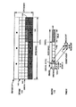
図4を参照すると、小バッファモードにおける画像140の一部分のブロック図が示されている。各小バッファ122は、画像140からの全1行未満のブロックを格納するように構成(設定)される。特に、小バッファ122は単一ブロックの高さ(例えばSROWINC)を有する。小バッファ122の幅(例えばSCOLMAXS)は、画像140の幅SCOLMAXより小さくてもよい。クライアントDMAモジュール126は、ローカルメモリ152とターゲット・ブロック148のみを処理するためにやり取り(送受信)する。
Referring to FIG. 4, a block diagram of a portion of
小バッファ122は、通常は第1の処理エンジン114−118と、外部DRAMメモリ・チップ104又は第2の処理エンジン114−118のいずれかとの間で転送される画像データをバッファするために使用される。小バッファ122は、通常、フレームの全幅をバッファすることによりオンチップ・メモリを浪費する逐次的に処理されるブロックであるフレームに対し有用である。小バッファ122は、外部メモリ・チップ104との長い待ち時間交換を、内部処理エンジン114−118のより短い待ち時間基準から分離するように使用することができる。共用のオンチップSMEMメモリ回路112内に小バッファ122とウインドウ・バッファ120との両方を実現することにより、より大きな柔軟性を付与して2つのタイプのバッファ間でメモリ空間と帯域幅を割り当てることができる。単一の高密度オンチップSMEM回路112アレイはまた、2つの別々のアレイより効率的に実現することができる。
The
DMAモジュール124と126は通常、2組のレジスタ(又はメモリ)160a−l60bにより制御される。レジスタ160aもまた、クライアントDMAレジスタ(又はメモリ)及びクライアント・オフセット・レジスタ(又はメモリ)と称されるものである。レジスタ160bもまた、外部DMAレジスタ(又はメモリ)及び外部オフセット・レジスタ(又はメモリ)と称されるものである。
DMAモジュール124と126は、画像処理用に最適化された2次元ブロック・データ転送を援助することができる。クライアントDMAレジスタ160aは、処理クライアント(処理エンジン114−118)とSMEM回路112間の転送を制御することができる。外部DMAレジスタ160bは外部メモリ・チップ104とSMEM回路112間の転送を制御することができる。SMEM回路112とDMAモジュール124、126は、外部メモリ・チップ104へアクセスする待ち時間が見えなくなる(隠れる)ように、通常(i)クライアントが読み込むためのDRAMデータのプリフェッチと、(ii)DRAMデータを外部メモリ・チップ104へ格納し戻すことを実施するべく一緒に接続される。
クライアント処理エンジン114−118及び別個のエンジン制御プロセッサ(図示せず)は通常、レジスタセット160a−160bのうち、特定セットのDMAレジスタ(チャネル)を指定する信号(例えばTRANS)でDMA要求を発行する。クライアントDMAレジスタ160aは、(i)ベース位置SBASEと、ウインドウ・バッファ120又は小バッファ122の高さSROWMAX及び幅SCOLMAX、又はSCOLMAXS、(ii)外部転送幅SBLKと転送されるデータ・ブロック144幅との比、そして(iii)ウインドウ・バッファ120内のデータ・ブロック144の水平オフセットSCOLと垂直オフセットSROWを指定することができる。ウインドウ・モード(例えば図2と図3)では、ウインドウ・バッファ120の幅と、外部メモリ・チップ104内に格納されるフレームの幅は一致してよい。小バッファ・モード(例えば図4)では、小バッファ122の幅SCOLMAXSと、外部メモリ・チップ104内のフレームの幅SCOLMAXDは、別々に指定することができる。ウインドウ・バッファ120に関わる転送要求は、付加的な水平オフセットと垂直オフセットとを指定する動きベクトル信号(例えばMV)を含むことができる。一般的には、動きベクトルのオフセット値により動き補償をDMA転送の一部として扱うことができる。ウインドウ・バッファ120の下位部分の開始場所を搬送する信号(例えばA)は、クライアントDMAモジュール126内にあり、アドレス信号(例えばADD)を生成する加算器164により動きベクトル値へ加算される。信号ADDは、クライアント・エンジン114−118へ転送するためにはウインドウ・バッファ120内の発見すべき適切なブロックの位置を関連(連結、連想)するクライアントDMAモジュール126に指示する。
The client processing engine 114-118 and a separate engine control processor (not shown) typically issue a DMA request with a signal (eg, TRANS) that specifies a particular set of DMA registers (channels) in the
各クライアント処理エンジン114−118及び個別のエンジン制御プロセッサは、DMAユニット110に対する未処理のDMA要求リストをキュー162a−162c内にそれぞれ保持する。DMAユニット110は、各キュー162a−162cからの要求を処理し、読み込みデータを返すか、格納データを検索する(引き出す)かのいずれかを行う。クライアントDMAモジュール126もまた、ウインドウ・バッファ・モードにおけるクライアントからの別の種類の要求を待ち行列に入れることができ、この要求は通常、関連するクライアントDMAモジュール126をウインドウ・バッファ120内の次のターゲット・ブロック148へ進ませる。通常、前記進行の結果、現在の水平オフセットSCOLをソフトウェアが指定した量(例えばSCOLCNT)だけインクリメントさせることとなる。しかしながら、前記インクリメントの結果、水平オフセットがウインドウ・バッファ120の幅に達すると、ターゲット・ブロック148の水平オフセットSCOLはゼロに設定され、現在の垂直オフセットSROWはソフトウェアに指定された量(例えばSROWINC)だけインクリメントすることができる。前記インクリメント要求もまた、どの外部DMAモジュール124(もしあれば)がクライアントDMAモジュール126に接続されるかを指定する。一般的には、別のインクリメント要求により、次のターゲット・ブロックに移動する前に現在のターゲット・ブロック148に対する多数の動き補償DMA要求を行うことが可能となる。
Each client processing engine 114-118 and individual engine control processor maintain a pending DMA request list for
クライアントDMAモジュール126は通常、小バッファ・モードにおける各正規のDMAモジュールがレジスタセット160a内に水平インクリメント量及び接続される外部DMAモジュール124の両方を指定した後、暗黙のインクリメント要求を行う。小バッファモードのDMAは通常、動き補償アクセス用には使用されないので、別個のインクリメント演算は通常実施されない。外部DMAモジュール124がクライアントDMAモジュール126に接続されると、外部メモリ回路104からの転送は、クライアントDMAモジュール126におけるある数のインクリメント後に、接続した外部DMAモジュール124により起動することができる。DMA要求ごとのインクリメント数はクライアントDMAレジスタ160aで指定することができる。
The
各処理エンジン114−118はダブルバンク・ローカルメモリRMEM及び/又はTMBMを実現し、DMA転送が1つのバンク(例えば152a)で行われるようにする一方で、エンジン114−118は他のバンク(例えば152b)のデータを処理する。通常は、ダブルバンク・ローカルメモリにより、SMEM回路112にアクセスする待ち時間を処理エンジン114−118から見えなくすることができる。通常、クライアント処理エンジン114−118とDMA処理間の同期は次のように扱われる。「最後の」ビットは、当該要求を現在のDMAバンクへの最後の要求として識別する信号TRANS内のDMA要求に含むことができる。DMAユニット110が「最後の」要求を完了すると、DMAユニット110は、クライアント(例えば114)が処理の完了を現在のメモリバンク(例えば152b)から示すまで待つ。同様にしてクライアント114は通常、クライアント114がバンク152b処理を完了した後、DMAユニット110が対応するメモリバンク(例えば152a)へのDMA転送を完了するのを待つ。クライアント114とDMAユニット110との両方の準備が整うと、バンク152aと152bとを交換することができる。クライアント114による処理はローカルメモリ・バンク152aから再開し、DMA転送はローカルメモリ・バンク152bにより再開することができる。
Each processing engine 114-118 implements a double bank local memory RMEM and / or TMBM, allowing DMA transfers to take place in one bank (eg 152a), while engines 114-118 152b) is processed. Usually, the double bank local memory can hide the latency to access the
外部DMAレジスタ160bは通常、(i)外部メモリ104におけるフレーム140のベース位置DBASETOP、及び高さDROWMAX、(ii)転送されるデータ・ブロック144のフレーム140内の水平オフセットDCOL及び垂直オフセットDROW、そして(iii)現在のSMEM行オフセットSROW(ウインドウ・モード)、又はSMEM列オフセットSCOL(小バッファモード)のいずれかを指定する。ウインドウ・モードに関しては、通常、現在のSMEM列オフセットSCOLは外部フレーム・オフセットと一致する。小バッファモードに関しては、SMEM行オフセットSROWは常にゼロであってよい。外部メモリ・チップ104転送の高さは、関連するSMEMクライアントDMAレジスタ160a転送の高さと同じであってよい。外部メモリ転送の幅は、SMEMインクリメントの数(関連するSMEMクライアントDMAレジスタ160a(SCNT)において指定された外部メモリ転送)を掛けたSMEM水平インクリメントの大きさSCOLCNTと一致する。従って、ある点後のプリフェッチ・リード/ライトと現在のターゲット・ブロック148間の一定の距離を維持することができる。
External DMA register 160b typically (i) base position DBASETOP and height DROWMAX of
一実施形態では、2つの外部メモリ要求は、各外部DMAモジュール124に対するキューに入れることができる。第1の外部メモリ要求は、同じMEMバッファにおいて転送されるデータに関わるクライアント転送要求とオーバーラップしてよい。クライアントが十分に高速であると、第2の外部メモリ要求を第1の要求の完了に先立って始動することができる。それゆえ後続のクライアントDMA転送は、第1の外部メモリ要求が終わるまで遮断することができる。通常、この遮断は、クライアント114−118がある点後の外部メモリプリフェッチ点又は外部メモリ書き込み点より先に進むことを防ぐことにより、外部メモリ転送及びSMEM転送間の同期を実現する。
In one embodiment, two external memory requests can be queued for each
1つの可能なアプリケーションでは、本発明は携帯用録画装置に適用することができる。例えば、本発明は、消費者市場に適した携帯型、高品位又は標準解像度のデジタル・ビデオ・カメラに組み込むことができる。一般的には、本発明のメモリ階層は高性能で、低電力のビデオ処理能力をカメラに提供する。ビデオ符号化/圧縮は、H.264/MPEG4-Advanced Video Coding standard、又は他の最新ビデオ符号化技術に準拠することができる。カメラ内蔵のメモリにより、1時間以上の高品位録画を実現できるであろう。本発明はまた、動き補償されたビデオ圧縮及び/又は復元を実施する任意のプロセッサに適する。本発明の他の応用を実施することにより特定の設計の基準を満たすことができる。 In one possible application, the present invention can be applied to a portable recording device. For example, the present invention can be incorporated into a portable, high definition or standard definition digital video camera suitable for the consumer market. In general, the memory hierarchy of the present invention provides high performance, low power video processing capabilities to the camera. Video encoding / compression can be compliant with H.264 / MPEG4-Advanced Video Coding standard, or other advanced video encoding technology. A camera built-in memory will be able to achieve high-quality recording for over an hour. The present invention is also suitable for any processor that performs motion compensated video compression and / or decompression. By implementing other applications of the present invention, certain design criteria can be met.
本発明はまた、ASIC、FPGAを作成することにより、従来の構成回路(ステートマシンを実施する従来の回路等)を適切なネットワークで相互に連結させることにより、又はここに説明されたようなハードウェアとソフトウェア要素の組合せにより実現でき、それらの変形は当業者には容易に理解できる。本明細書で使用された用語「同時に」は、ある共通の期間を共有する事象を説明することを意味するが、この用語は同じ時点に始まり、同じ時点に終わる事象、又は同じ期間を有する事象に限定されることを意味しない。 The present invention also provides for creating ASICs, FPGAs, interconnecting conventional configuration circuits (such as conventional circuits implementing state machines) with appropriate networks, or hardware as described herein. It can be realized by a combination of hardware and software elements, and variations thereof can be easily understood by those skilled in the art. As used herein, the term “simultaneously” is meant to describe events that share a common time period, but this term is an event that starts at the same time and ends at the same time, or an event that has the same time Does not mean to be limited to.
本発明はその好ましい実施例を参照して特に図示され、説明されたが、その形態と詳細において様々な変更が、本発明の精神及び範囲から逸脱することなく行うことができることは当業者には理解されるであろう。 Although the present invention has been particularly shown and described with reference to preferred embodiments thereof, it will be apparent to those skilled in the art that various changes in form and detail can be made without departing from the spirit and scope of the invention. Will be understood.
100 システム
102 ビデオチップ
104 外部メモリ・チップ
106 インタフェース
108 インタフェース
110 ダイレクトメモリアクセス(DMA)ユニット
112 共有メモリ回路
114 動き予測(ME)エンジン
116 クライアント・エンジン
118 処理エンジン
120 ウインドウ・バッファ
122 小バッファ
124 外部DMA回路
126 クライアントDMA回路
140 画像
148 ターゲット・ブロック
152a−152n ローカルメモリ
152 ローカルメモリ
160a クライアントDMAレジスタ
160b 外部DMAレジスタ
RMEM 基準メモリ
TMEM ターゲットメモリ
100
Claims (20)
前記チップ上に配置されるとともに、(i)前記サブセットを前記外部メモリから前記内部メモリへ転送し(ii)前記第1のバッファにおける前記ブロックの古いセットの処理が完了したとき、前記ブロックの新しいセットを前記外部メモリから前記第1のバッファに転送するように構成された外部転送回路と、
を備え、
(1)前記新しいセットのサイズが(a)前記古いセットのサイズと一致し(b)前記第1のバッファの一部分を占め、(2)ターゲットフレームと前記基準フレームとの間の複数個の動き予測を容易にするように、前記基準フレーム内の前記ブロックのそれぞれが1ターゲットフレームごとに一回だけ前記外部メモリから前記第1のバッファへ転送されることを特徴とする装置。 Disposed on the chip and including at least one first buffer for (i) applying motion compensation and (ii) storing a subset of at least one reference frame stored in external memory outside the chip An internal memory, wherein the at least one first buffer has a size larger than one row of the block of the reference frame;
And (i) transfer the subset from the external memory to the internal memory; and (ii) complete processing of the old set of blocks in the first buffer when the new set of blocks is complete. An external transfer circuit configured to transfer a set from the external memory to the first buffer;
With
(1) the size of the new set matches (a) the size of the old set, (b) occupies a portion of the first buffer, and (2) a plurality of movements between the target frame and the reference frame The apparatus, wherein each of the blocks in the reference frame is transferred from the external memory to the first buffer only once per target frame to facilitate prediction.
(ii)前記外部メモリと前記内部メモリ間の転送は、前記内部メモリと前記処理エンジン間で転送を行うための前記少なくとも1つのクライアント・オフセット・メモリへの信号に基づいて開始される請求項8に記載の装置。 (I) at least one of the external offset memories is connected to at least one of a plurality of client offset memories;
The transfer between the external memory and the internal memory is initiated based on a signal to the at least one client offset memory for transferring between the internal memory and the processing engine. The device described in 1.
前記チップ上に配置されるとともに、前記内部メモリからの前記サブセットの少なくとも一部分に作用するように構成された第1の処理エンジンと、
を備え、
ターゲットフレームと前記基準フレームとの間の複数個の動き予測を容易にするように、前記基準フレーム内の前記ブロックのそれぞれが1ターゲットフレームごとに一回だけ前記外部メモリから前記第1のバッファへ転送されることを特徴とする装置。 An internal memory comprising: a first buffer disposed on a chip and comprising: (i) applying motion compensation; and (ii) storing a subset of at least one reference frame stored in an external memory outside the chip. (A) the width of the first buffer matches the width of the reference frame, the height of the first buffer is higher than one block row, and (b) a new set of blocks is Received from the external memory when processing of the old set of blocks in the first buffer is complete, (c) the size of the new set matches (1) the size of the old set, and (2) the first Internal memory occupying part of the buffer
A first processing engine disposed on the chip and configured to act on at least a portion of the subset from the internal memory;
With
To facilitate a plurality of motion predictions between a target frame and the reference frame, each of the blocks in the reference frame is transferred from the external memory to the first buffer only once per target frame. A device characterized by being transferred.
Applications Claiming Priority (2)
| Application Number | Priority Date | Filing Date | Title |
|---|---|---|---|
| US11/078,779 US7536487B1 (en) | 2005-03-11 | 2005-03-11 | Low power memory hierarchy for high performance video processor |
| US11/078,779 | 2005-03-11 |
Related Parent Applications (1)
| Application Number | Title | Priority Date | Filing Date |
|---|---|---|---|
| JP2006057833A Division JP5300176B2 (en) | 2005-03-11 | 2006-03-03 | Low power memory hierarchy for high performance video processors |
Publications (2)
| Publication Number | Publication Date |
|---|---|
| JP2013055703A JP2013055703A (en) | 2013-03-21 |
| JP5245004B2 true JP5245004B2 (en) | 2013-07-24 |
Family
ID=36609333
Family Applications (2)
| Application Number | Title | Priority Date | Filing Date |
|---|---|---|---|
| JP2006057833A Active JP5300176B2 (en) | 2005-03-11 | 2006-03-03 | Low power memory hierarchy for high performance video processors |
| JP2012273316A Active JP5245004B2 (en) | 2005-03-11 | 2012-12-14 | Low power memory hierarchy for high performance video processors |
Family Applications Before (1)
| Application Number | Title | Priority Date | Filing Date |
|---|---|---|---|
| JP2006057833A Active JP5300176B2 (en) | 2005-03-11 | 2006-03-03 | Low power memory hierarchy for high performance video processors |
Country Status (3)
| Country | Link |
|---|---|
| US (1) | US7536487B1 (en) |
| EP (1) | EP1701550A3 (en) |
| JP (2) | JP5300176B2 (en) |
Families Citing this family (12)
| Publication number | Priority date | Publication date | Assignee | Title |
|---|---|---|---|---|
| JP4922839B2 (en) * | 2007-06-04 | 2012-04-25 | 三洋電機株式会社 | Signal processing apparatus, video display apparatus, and signal processing method |
| US8547445B1 (en) | 2010-02-17 | 2013-10-01 | Ambarella, Inc. | Camera using combined color processing in lookup |
| US8531549B1 (en) | 2010-02-25 | 2013-09-10 | Ambarella, Inc. | Camera that uses YUV to YUV table-based color correction for processing digital images |
| US8508624B1 (en) | 2010-03-19 | 2013-08-13 | Ambarella, Inc. | Camera with color correction after luminance and chrominance separation |
| US8659683B1 (en) | 2010-03-25 | 2014-02-25 | Ambarella, Inc. | Digital picture noise reduction by combining high-noise and low-noise processed pictures |
| US8675086B1 (en) | 2010-03-26 | 2014-03-18 | Ambarella, Inc. | Architecture for video, fast still and high quality still picture processing |
| EP2617186B1 (en) | 2010-09-13 | 2021-11-03 | Contour IP Holding, LLC | Portable digital video camera configured for remote image acquisition control and viewing |
| TW201215149A (en) * | 2010-09-17 | 2012-04-01 | Alpha Imaging Technology Corp | Notebook computer for processing original high resolution images and image processing device thereof |
| US8447134B1 (en) | 2010-12-20 | 2013-05-21 | Ambarella, Inc. | Image warp caching |
| KR101996641B1 (en) | 2012-02-06 | 2019-07-04 | 삼성전자주식회사 | Apparatus and method for memory overlay |
| US10558599B2 (en) * | 2017-09-12 | 2020-02-11 | Nxp Usa, Inc. | Method and apparatus for loading a matrix into an accelerator |
| US11234017B1 (en) * | 2019-12-13 | 2022-01-25 | Meta Platforms, Inc. | Hierarchical motion search processing |
Family Cites Families (22)
| Publication number | Priority date | Publication date | Assignee | Title |
|---|---|---|---|---|
| JPS61251967A (en) * | 1985-04-30 | 1986-11-08 | Fanuc Ltd | Image processor |
| JPH02190968A (en) * | 1989-01-19 | 1990-07-26 | Nec Corp | Vector processor |
| JP3605891B2 (en) * | 1995-06-29 | 2004-12-22 | セイコーエプソン株式会社 | Computer system |
| US6335950B1 (en) * | 1997-10-14 | 2002-01-01 | Lsi Logic Corporation | Motion estimation engine |
| US6563549B1 (en) * | 1998-04-03 | 2003-05-13 | Sarnoff Corporation | Method and apparatus for adaptively encoding an information stream |
| JP2000010856A (en) * | 1998-06-19 | 2000-01-14 | Asahi Chem Ind Co Ltd | Memory controller |
| JP2000287214A (en) * | 1999-03-31 | 2000-10-13 | Toshiba Corp | Method and unit for motion detection |
| JP2001101396A (en) * | 1999-09-30 | 2001-04-13 | Toshiba Corp | Processor and method for correcting image distortion and medium with program performing image distortion correction processing stored therein |
| US6859494B2 (en) * | 2001-07-27 | 2005-02-22 | General Instrument Corporation | Methods and apparatus for sub-pixel motion estimation |
| JP2003070000A (en) * | 2001-08-23 | 2003-03-07 | Matsushita Electric Ind Co Ltd | Image encoder |
| US20030103567A1 (en) * | 2001-12-03 | 2003-06-05 | Riemens Abraham Karel | Motion compensation and/or estimation |
| US6683614B2 (en) * | 2001-12-21 | 2004-01-27 | Hewlett-Packard Development Company, L.P. | System and method for automatically configuring graphics pipelines by tracking a region of interest in a computer graphical display system |
| JP2004005287A (en) * | 2002-06-03 | 2004-01-08 | Hitachi Ltd | Processor system with coprocessor |
| JP2004013389A (en) * | 2002-06-05 | 2004-01-15 | Sony Corp | System and method for data transfer |
| JP4195969B2 (en) * | 2002-08-05 | 2008-12-17 | パナソニック株式会社 | Motion vector detection device |
| JP2004126873A (en) * | 2002-10-01 | 2004-04-22 | Sony Corp | Information processor and method, storage medium, and program |
| TWI249356B (en) * | 2002-11-06 | 2006-02-11 | Nokia Corp | Picture buffering for prediction references and display |
| JP2004356673A (en) * | 2003-05-26 | 2004-12-16 | Sony Corp | Motion vector detecting method and image processing apparatus using the method |
| US20040258147A1 (en) * | 2003-06-23 | 2004-12-23 | Tsu-Chang Lee | Memory and array processor structure for multiple-dimensional signal processing |
| US20050129121A1 (en) * | 2003-12-01 | 2005-06-16 | Chih-Ta Star Sung | On-chip image buffer compression method and apparatus for digital image compression |
| US20060050976A1 (en) * | 2004-09-09 | 2006-03-09 | Stephen Molloy | Caching method and apparatus for video motion compensation |
| US8311088B2 (en) * | 2005-02-07 | 2012-11-13 | Broadcom Corporation | Method and system for image processing in a microprocessor for portable video communication devices |
-
2005
- 2005-03-11 US US11/078,779 patent/US7536487B1/en active Active
- 2005-11-12 EP EP05256994.4A patent/EP1701550A3/en not_active Ceased
-
2006
- 2006-03-03 JP JP2006057833A patent/JP5300176B2/en active Active
-
2012
- 2012-12-14 JP JP2012273316A patent/JP5245004B2/en active Active
Also Published As
| Publication number | Publication date |
|---|---|
| JP2013055703A (en) | 2013-03-21 |
| EP1701550A3 (en) | 2014-10-15 |
| EP1701550A2 (en) | 2006-09-13 |
| US7536487B1 (en) | 2009-05-19 |
| JP5300176B2 (en) | 2013-09-25 |
| JP2006254437A (en) | 2006-09-21 |
Similar Documents
| Publication | Publication Date | Title |
|---|---|---|
| JP5245004B2 (en) | Low power memory hierarchy for high performance video processors | |
| KR100881539B1 (en) | Image data structure for direct memory access | |
| US8175157B2 (en) | Apparatus and method for controlling data write/read in image processing system | |
| KR100606812B1 (en) | Video decoding system | |
| US20070071099A1 (en) | External memory device, method of storing image data for the same, and image processor using the method | |
| US9530387B2 (en) | Adjusting direct memory access transfers used in video decoding | |
| US8483279B2 (en) | Moving image parallel processor having deblocking filters | |
| JPH06225292A (en) | Module memory for image decoding system | |
| EP0602642B1 (en) | Moving picture decoding system | |
| Li et al. | Architecture and bus-arbitration schemes for MPEG-2 video decoder | |
| US8045021B2 (en) | Memory organizational scheme and controller architecture for image and video processing | |
| US7330595B2 (en) | System and method for video data compression | |
| US20030123555A1 (en) | Video decoding system and memory interface apparatus | |
| JP2009130599A (en) | Moving picture decoder | |
| KR100708183B1 (en) | Image storing device for motion prediction, and method for storing data of the same | |
| Li et al. | Design of memory sub-system with constant-rate bumping process for H. 264/AVC decoder | |
| KR100504507B1 (en) | Apparatus for video decoding | |
| US20130322551A1 (en) | Memory Look Ahead Engine for Video Analytics | |
| US20090310683A1 (en) | Video coding device and video coding method | |
| Wang et al. | SDRAM bus schedule of HDTV video decoder | |
| KR100288141B1 (en) | Memory connection device of MPEG video encoder | |
| JP2005229423A (en) | Apparatus for inverse orthogonal transformation |
Legal Events
| Date | Code | Title | Description |
|---|---|---|---|
| A621 | Written request for application examination |
Free format text: JAPANESE INTERMEDIATE CODE: A621 Effective date: 20121214 |
|
| A871 | Explanation of circumstances concerning accelerated examination |
Free format text: JAPANESE INTERMEDIATE CODE: A871 Effective date: 20121214 |
|
| A975 | Report on accelerated examination |
Free format text: JAPANESE INTERMEDIATE CODE: A971005 Effective date: 20130107 |
|
| TRDD | Decision of grant or rejection written | ||
| A01 | Written decision to grant a patent or to grant a registration (utility model) |
Free format text: JAPANESE INTERMEDIATE CODE: A01 Effective date: 20130312 |
|
| A61 | First payment of annual fees (during grant procedure) |
Free format text: JAPANESE INTERMEDIATE CODE: A61 Effective date: 20130408 |
|
| FPAY | Renewal fee payment (event date is renewal date of database) |
Free format text: PAYMENT UNTIL: 20160412 Year of fee payment: 3 |
|
| R150 | Certificate of patent or registration of utility model |
Free format text: JAPANESE INTERMEDIATE CODE: R150 Ref document number: 5245004 Country of ref document: JP Free format text: JAPANESE INTERMEDIATE CODE: R150 |
|
| R250 | Receipt of annual fees |
Free format text: JAPANESE INTERMEDIATE CODE: R250 |
|
| R250 | Receipt of annual fees |
Free format text: JAPANESE INTERMEDIATE CODE: R250 |
|
| R250 | Receipt of annual fees |
Free format text: JAPANESE INTERMEDIATE CODE: R250 |
|
| R250 | Receipt of annual fees |
Free format text: JAPANESE INTERMEDIATE CODE: R250 |
|
| R250 | Receipt of annual fees |
Free format text: JAPANESE INTERMEDIATE CODE: R250 |
|
| S111 | Request for change of ownership or part of ownership |
Free format text: JAPANESE INTERMEDIATE CODE: R313113 |
|
| S531 | Written request for registration of change of domicile |
Free format text: JAPANESE INTERMEDIATE CODE: R313531 |
|
| R350 | Written notification of registration of transfer |
Free format text: JAPANESE INTERMEDIATE CODE: R350 |
|
| R250 | Receipt of annual fees |
Free format text: JAPANESE INTERMEDIATE CODE: R250 |
|
| R250 | Receipt of annual fees |
Free format text: JAPANESE INTERMEDIATE CODE: R250 |
|
| R250 | Receipt of annual fees |
Free format text: JAPANESE INTERMEDIATE CODE: R250 |
|
| R250 | Receipt of annual fees |
Free format text: JAPANESE INTERMEDIATE CODE: R250 |