JP5241173B2 - Manufacturing method of organic EL element - Google Patents
Manufacturing method of organic EL element Download PDFInfo
- Publication number
- JP5241173B2 JP5241173B2 JP2007220813A JP2007220813A JP5241173B2 JP 5241173 B2 JP5241173 B2 JP 5241173B2 JP 2007220813 A JP2007220813 A JP 2007220813A JP 2007220813 A JP2007220813 A JP 2007220813A JP 5241173 B2 JP5241173 B2 JP 5241173B2
- Authority
- JP
- Japan
- Prior art keywords
- layer
- passivation layer
- organic
- film
- forming
- Prior art date
- Legal status (The legal status is an assumption and is not a legal conclusion. Google has not performed a legal analysis and makes no representation as to the accuracy of the status listed.)
- Expired - Fee Related
Links
Images


Classifications
-
- H—ELECTRICITY
- H10—SEMICONDUCTOR DEVICES; ELECTRIC SOLID-STATE DEVICES NOT OTHERWISE PROVIDED FOR
- H10K—ORGANIC ELECTRIC SOLID-STATE DEVICES
- H10K50/00—Organic light-emitting devices
- H10K50/10—OLEDs or polymer light-emitting diodes [PLED]
- H10K50/17—Carrier injection layers
- H10K50/171—Electron injection layers
-
- H—ELECTRICITY
- H10—SEMICONDUCTOR DEVICES; ELECTRIC SOLID-STATE DEVICES NOT OTHERWISE PROVIDED FOR
- H10K—ORGANIC ELECTRIC SOLID-STATE DEVICES
- H10K50/00—Organic light-emitting devices
- H10K50/80—Constructional details
- H10K50/84—Passivation; Containers; Encapsulations
- H10K50/841—Self-supporting sealing arrangements
-
- H—ELECTRICITY
- H10—SEMICONDUCTOR DEVICES; ELECTRIC SOLID-STATE DEVICES NOT OTHERWISE PROVIDED FOR
- H10K—ORGANIC ELECTRIC SOLID-STATE DEVICES
- H10K50/00—Organic light-emitting devices
- H10K50/80—Constructional details
- H10K50/84—Passivation; Containers; Encapsulations
- H10K50/842—Containers
- H10K50/8426—Peripheral sealing arrangements, e.g. adhesives, sealants
-
- H—ELECTRICITY
- H10—SEMICONDUCTOR DEVICES; ELECTRIC SOLID-STATE DEVICES NOT OTHERWISE PROVIDED FOR
- H10K—ORGANIC ELECTRIC SOLID-STATE DEVICES
- H10K50/00—Organic light-emitting devices
- H10K50/80—Constructional details
- H10K50/84—Passivation; Containers; Encapsulations
- H10K50/844—Encapsulations
-
- H—ELECTRICITY
- H10—SEMICONDUCTOR DEVICES; ELECTRIC SOLID-STATE DEVICES NOT OTHERWISE PROVIDED FOR
- H10K—ORGANIC ELECTRIC SOLID-STATE DEVICES
- H10K59/00—Integrated devices, or assemblies of multiple devices, comprising at least one organic light-emitting element covered by group H10K50/00
- H10K59/80—Constructional details
- H10K59/87—Passivation; Containers; Encapsulations
- H10K59/871—Self-supporting sealing arrangements
-
- H—ELECTRICITY
- H10—SEMICONDUCTOR DEVICES; ELECTRIC SOLID-STATE DEVICES NOT OTHERWISE PROVIDED FOR
- H10K—ORGANIC ELECTRIC SOLID-STATE DEVICES
- H10K59/00—Integrated devices, or assemblies of multiple devices, comprising at least one organic light-emitting element covered by group H10K50/00
- H10K59/80—Constructional details
- H10K59/87—Passivation; Containers; Encapsulations
- H10K59/873—Encapsulations
-
- H—ELECTRICITY
- H10—SEMICONDUCTOR DEVICES; ELECTRIC SOLID-STATE DEVICES NOT OTHERWISE PROVIDED FOR
- H10K—ORGANIC ELECTRIC SOLID-STATE DEVICES
- H10K2102/00—Constructional details relating to the organic devices covered by this subclass
- H10K2102/301—Details of OLEDs
- H10K2102/302—Details of OLEDs of OLED structures
- H10K2102/3023—Direction of light emission
- H10K2102/3026—Top emission
-
- H—ELECTRICITY
- H10—SEMICONDUCTOR DEVICES; ELECTRIC SOLID-STATE DEVICES NOT OTHERWISE PROVIDED FOR
- H10K—ORGANIC ELECTRIC SOLID-STATE DEVICES
- H10K50/00—Organic light-emitting devices
- H10K50/80—Constructional details
- H10K50/86—Arrangements for improving contrast, e.g. preventing reflection of ambient light
-
- H—ELECTRICITY
- H10—SEMICONDUCTOR DEVICES; ELECTRIC SOLID-STATE DEVICES NOT OTHERWISE PROVIDED FOR
- H10K—ORGANIC ELECTRIC SOLID-STATE DEVICES
- H10K59/00—Integrated devices, or assemblies of multiple devices, comprising at least one organic light-emitting element covered by group H10K50/00
- H10K59/80—Constructional details
- H10K59/8791—Arrangements for improving contrast, e.g. preventing reflection of ambient light
Landscapes
- Physics & Mathematics (AREA)
- Optics & Photonics (AREA)
- Electroluminescent Light Sources (AREA)
Description
本発明は、フラットパネルディスプレイ等に用いられる有機EL素子の製造方法に関する。 The present invention relates to a method of manufacturing an organic EL element used in a flat panel display or the like.
近年、フラットパネルディスプレイとして、自発光型デバイスである有機EL素子が、注目されている。有機EL素子は、水分や酸素により、特性劣化を招き易く、わずかな水分により、有機化合物層と電極層の剥離が生じダークスポット発生の原因となる。そのため、有機EL素子をエッチングガラスカバーで覆い、シール剤により周辺を貼り付け、内部に吸湿剤を装着して、シール面から浸入する水分を、吸湿剤で吸湿し、有機EL素子の寿命を確保している。 In recent years, organic EL elements, which are self-luminous devices, have attracted attention as flat panel displays. The organic EL element easily deteriorates in characteristics due to moisture and oxygen, and a slight amount of moisture causes peeling of the organic compound layer and the electrode layer, which causes dark spots. Therefore, the organic EL element is covered with an etching glass cover, the periphery is pasted with a sealing agent, a moisture absorbent is attached inside, and moisture that enters from the sealing surface is absorbed by the moisture absorbent to ensure the life of the organic EL element. doing.
しかし、薄型の有機EL素子による省スペースのフラットパネルディスプレイを実現するためには、発光エリア周辺の吸湿剤のスペースを無くし、さらに薄型化を図っていかなければならず、大量の吸湿剤を必要としない有機EL素子の封止方法が必要である。そのため、水分や酸素の有機化合物層への浸入を防止するための高機能なパッシべーション層による固体封止が要求されている。 However, in order to realize a space-saving flat panel display with thin organic EL elements, it is necessary to eliminate the space of the hygroscopic agent around the light emitting area and to make it thinner, and a large amount of hygroscopic agent is required. An organic EL element sealing method is not required. Therefore, solid sealing with a highly functional passivation layer for preventing intrusion of moisture and oxygen into the organic compound layer is required.
これらの問題を解決する為、近年、有機EL素子のパッシべーション層として、CVD法やスパッタ法を用いた酸化窒化シリコン膜や、セラミックと有機膜を積層させたパッシべーション層による固体封止が提案されている。 In order to solve these problems, in recent years, as a passivation layer of an organic EL element, a silicon oxynitride film using a CVD method or a sputtering method, or a solid sealing by a passivation layer in which a ceramic and an organic film are laminated Has been proposed.
特許文献1によれば、プラズマCVD法を用いて窒化シリコン膜からなるパッシべーション層で封止した有機EL素子が提案されている。
According to
特許文献2によれば、CVD法により形成された窒化シリコン膜からなるパッシべーション層の技術が提案されている。
According to
さらに、特許文献3によれば、電子注入層の界面にセシウムを添加した素子に、蒸着法により窒化シリコン膜、又はITO材料からなる封止膜を形成する技術が提案されている。
Further, according to
一般に、有機EL素子は、アノードと、正孔輸送層、発光層、電子輸送層、電子注入層からなる有機化合物層と、カソード、そしてこれらを水分から保護するパッシべーション層で構成される。そして有機EL素子の電子注入層には、有機化合物材料と、アルカリ金属化合物とを共蒸着して形成されたアルカリ金属、又はアルカリ金属化合物が含まれる。このようにアルカリ金属を有する電子注入層を形成し、電子注入効率を高めている。 In general, an organic EL device includes an anode, an organic compound layer including a hole transport layer, a light emitting layer, an electron transport layer, and an electron injection layer, a cathode, and a passivation layer that protects these from moisture. The electron injection layer of the organic EL element contains an alkali metal or an alkali metal compound formed by co-evaporation of an organic compound material and an alkali metal compound. Thus, an electron injection layer having an alkali metal is formed to increase the electron injection efficiency.
ところが、アルカリ金属化合物と有機化合物材料とを共蒸着する際に、アルカリ金属化合物のクラスター(塊)が有機EL素子中に付着する。 However, when the alkali metal compound and the organic compound material are co-evaporated, the alkali metal compound clusters (lumps) adhere to the organic EL element.
その上には、酸化インジウム酸化錫合金(ITO)や酸化インジウム酸化亜鉛合金(IZO)、酸化インジウム錫亜鉛合金(ITZO)等の酸化膜からなるカソードが形成される。さらに上に、水素及び水素を含む材料ガスを用いて、パッシべーション層を形成すると、素子上にボイドが生じる。このボイドは、数μm程度から数十μmの大きさとなる。さらに膨張して破裂する場合もある。このようなボイドは、パッシべーション層に、水分の浸入経路となる亀裂を生じさせる事が多く、有機EL素子にダークスポットを発生させる原因となる。 A cathode made of an oxide film such as an indium tin oxide alloy (ITO), an indium zinc oxide alloy (IZO), an indium tin oxide zinc alloy (ITZO) is formed thereon. Further, when a passivation layer is formed using hydrogen and a material gas containing hydrogen, voids are generated on the device. This void has a size of about several μm to several tens of μm. Furthermore, it may expand and rupture. Such voids often cause cracks in the passivation layer to become moisture infiltration paths, and cause dark spots in the organic EL element.
上述したように、特許文献3には、電子注入層の界面にセシウムを添加した素子に、蒸着法により窒化シリコン膜、又はITO材料からなるパッシべーション層を形成する技術が提案されている。ところが、有機EL素子上には、有機化合物層を蒸着形成する際に発生するクラスターや、素子分離膜のエッチング残渣等の異物が付着している。蒸着法やスパッタリング法で形成した窒化シリコン膜やITO膜からなるパッシべーション層は、膜が固くカバレッジ性能が不十分で上記の異物上に形成すると、異物をカバーしきれない。膜厚を厚くすると、封止膜に亀裂が発生する、割れる等の問題が生じ、水分や酸素の浸入を防止するには不十分である。
As described above,
本発明は、有機EL素子の製造工程で発生するボイドを抑え、有機EL素子の有機化合物層への水分や酸素の浸入を防止することができる有機EL素子及びその製造方法を提供することである。 An object of the present invention is to provide an organic EL element capable of suppressing voids generated in the manufacturing process of the organic EL element and preventing intrusion of moisture and oxygen into the organic compound layer of the organic EL element, and a method for manufacturing the organic EL element. .
上記課題を解決するための手段として、本発明の有機EL素子の製造方法は、
基板の上に下部電極と有機化合物層と上部電極とを積層する工程と、それらを覆うパッシベーション層を形成する工程とを、少なくとも有する有機EL素子の製造方法において、
前記有機化合物層のうち電子注入層がアルカリ金属又はアルカリ金属化合物を含有し、前記上部電極は酸化膜からなり、
前記積層する工程は、前記電子注入層を形成する工程と、前記電子注入層の直上に前記上部電極を形成する工程とを含み、
前記パッシベーション層を形成する工程は、前記上部電極の直上に珪素を含みかつ水素を含まない材料を用いて第一パッシベーション層を形成する工程と、前記第一パッシベーション層の上に珪素および水素を含む材料を用いて、CVD法により第二パッシベーション層を形成する工程とを含むことを特徴とする。
As a means for solving the above problems, the method for producing an organic EL element of the present invention comprises:
In the method of manufacturing an organic EL element, the method includes: a step of laminating a lower electrode, an organic compound layer, and an upper electrode on a substrate; and a step of forming a passivation layer that covers them.
Of the organic compound layer, the electron injection layer contains an alkali metal or an alkali metal compound, and the upper electrode is made of an oxide film,
The step of laminating includes a step of forming the electron injection layer, and a step of forming the upper electrode directly on the electron injection layer,
The step of forming the passivation layer includes a step of forming a first passivation layer using a material that contains silicon and does not contain hydrogen immediately above the upper electrode, and includes silicon and hydrogen on the first passivation layer. And a step of forming a second passivation layer by a CVD method using a material .
本発明によれば、有機EL素子の製造工程で発生するボイドを抑え、有機EL素子の有機化合物層への水分や酸素の浸入を防止することができる。 ADVANTAGE OF THE INVENTION According to this invention, the void which generate | occur | produces in the manufacturing process of an organic EL element can be suppressed, and the penetration | invasion of the water | moisture content and oxygen to the organic compound layer of an organic EL element can be prevented.
先ず、本発明に至った経緯について説明し、その後、本発明の有機EL素子及びその製造方法について、詳細に説明する。 First, the background that led to the present invention will be described, and then the organic EL element of the present invention and the manufacturing method thereof will be described in detail.
電子注入層にアルカリ金属やアルカリ金属化合物をドープした有機EL素子は、有機化合物とアルカリ金属化合物とを共蒸着する際に、有機EL素子の蒸着面にアルカリ金属化合物のクラスターが付着する場合が多い。その電子注入層上に上部電極を形成するが、上記クラスターは膜厚の薄い上部電極では覆い隠せないし、水の通過を防止することが不十分と考えられる。そのため、アルカリ金属やアルカリ金属化合物を含む電子注入層の上に酸化物からなる上部電極を形成して構成された有機EL素子は、上部電極の上にパッシべーション層を形成すると、有機EL素子中にボイドが発生する。これは、パッシべーション層を形成する際に、使用する材料ガスに水素が含まれていると、発生した水素イオンやラジカルが下地の酸化物の酸素を引抜き水やOH基が生成される。この水やOH基が上部電極の隙間から入り込んでアルカリ金属やアルカリ金属化合物を多量に含むクラスターと反応して、例えば(1)のような反応に基づき水素が発生し、この水素がボイドを形成すると考えられる。 In an organic EL device in which an electron injection layer is doped with an alkali metal or an alkali metal compound, when an organic compound and an alkali metal compound are co-evaporated, a cluster of alkali metal compounds often adheres to the vapor deposition surface of the organic EL device. . An upper electrode is formed on the electron injection layer, but the cluster cannot be covered with the thin upper electrode, and it is considered insufficient to prevent the passage of water. Therefore, when an organic EL element formed by forming an upper electrode made of an oxide on an electron injection layer containing an alkali metal or an alkali metal compound is formed on the upper electrode, the organic EL element Voids are generated inside. This is because, when forming the passivation layer, if the material gas used contains hydrogen, the generated hydrogen ions and radicals draw oxygen from the underlying oxide to produce water and OH groups. This water or OH group enters through the gap between the upper electrodes and reacts with a cluster containing a large amount of alkali metal or alkali metal compound. For example, hydrogen is generated based on the reaction (1), and this hydrogen forms a void. I think that.
2Cs+2H2O → 2Cs(OH)+H2‥(1) 2C s + 2H 2 O → 2Cs (OH) + H 2 (1)
電子注入層にドープされるアルカリ金属やアルカリ金属化合物、特に水分との反応性の高いセシウム又はセシウム化合物を用いた場合、ボイドの大きさや発生率は高くなる。さらに、セシウム又はセシウム化合物を電子注入層にドープする際、共蒸着材料に炭酸セシウムを用いると、ボイドの大きさや、発生率が特に高まる。 When an alkali metal or an alkali metal compound doped in the electron injection layer, particularly a cesium or cesium compound highly reactive with moisture, the size and incidence of voids are increased. Furthermore, when cesium carbonate is used as the co-evaporation material when doping the electron injection layer with cesium or a cesium compound, the size and generation rate of voids are particularly increased.
有機EL素子の上部電極の上に、膜中の水素やプラズマ中の水素イオン及びラジカルの保護の役割を持たせた第一パッシベーション層を形成する。そして、その上にカバレッジ性能及び防湿性能の高い第二パッシベーション層を形成すれば、ボイドの発生を抑えたパッシベーション層が実現できると、本発明者は考える。 A first passivation layer having a role of protecting hydrogen in the film, hydrogen ions in plasma and radicals is formed on the upper electrode of the organic EL element. Then, the present inventor believes that if a second passivation layer having high coverage performance and moisture proof performance is formed thereon, a passivation layer in which generation of voids is suppressed can be realized.
よって、第一パッシべーション層は、水素イオンやラジカルの発生しない製法で水素を含まないパッシべーション層とし、水素及び水素イオンやラジカルがボイドを形成しないようにした。また、水素を含むパッシべーション層は水素含有量を多くすると膜中の空孔は増加し、サイズも大きくなり、異物への着き回りが良く、平坦化性、カバレッジ性が高まる。さらに、水素含有量を減少させれば膜中の空孔は逆の傾向を示し、防湿性が高まる。よって、第二パッシべーション層は水素を含むことが望ましい。 Therefore, the first passivation layer is a passivation layer that does not contain hydrogen by a method that does not generate hydrogen ions and radicals, and hydrogen, hydrogen ions, and radicals do not form voids. In addition, when the hydrogen content is increased in the passivation layer containing hydrogen, the number of pores in the film increases, the size increases, the contact with foreign matters is improved, and the flatness and coverage are improved. Furthermore, if the hydrogen content is decreased, the vacancies in the film show the opposite tendency, and the moisture resistance increases. Therefore, it is desirable that the second passivation layer contains hydrogen.
以下に、本発明の有機EL素子の実施形態を、図面を参照しつつ、製造方法に沿って説明するが、本発明はこれらの実施形態に限るものではない。 Hereinafter, embodiments of the organic EL element of the present invention will be described along a manufacturing method with reference to the drawings. However, the present invention is not limited to these embodiments.
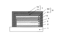
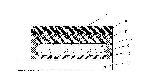
図1から図6は本発明の有機EL素子の断面の一部を表す一例の概念図である。 FIG. 1 to FIG. 6 are conceptual diagrams of examples showing a part of the cross section of the organic EL element of the present invention.
先ず、ガラス基板上に不図示のTFT、絶縁膜、有機平坦化膜の順で積層形成した基板1上に画素単位の下部電極2であるCr電極を形成する。その各画素の周囲を例えばポリイミドや窒化珪素等の絶縁材料から成る不図示の素子分離膜で覆う。下部電極2は、アルミニウムや銀とIZO、ITOなどの酸化膜の積層であっても良い。
First, a Cr electrode, which is a
この基板1上に正孔輸送層、発光層、電子輸送層から成る有機化合物層3と、電子注入層4の有機化合物層とを順次形成する。電子注入層4は、アルカリ金属やアルカリ金属化合物をドープすることで、電子注入効率を高めることができる。
An
前記アルカリ金属又はアルカリ金属化合物としてはセシウム又はセシウム化合物を用いることができる。ここで、前記セシウム化合物は、炭酸セシウム、及びセシウムサブオキサイド等の炭酸セシウム由来の物質、及びセシウムが前記有機化合物に配位した配位化合物からなる群の中から選択される少なくとも一つである。 As the alkali metal or alkali metal compound, cesium or a cesium compound can be used. Here, the cesium compound is at least one selected from the group consisting of a substance derived from cesium carbonate such as cesium carbonate and cesium suboxide, and a coordination compound in which cesium is coordinated to the organic compound. .
つまり、電子注入層4は、ナトリウム、リチウム、カリウム、ルビジウム、セシウム、フランシウムの金属やそれらの化合物と有機化合物とを共蒸着して形成できるのである。本実施形態では、セシウム化合物の炭酸セシウムと電子輸送性材料とを共蒸着してセシウム化合物を0.1〜数十%含有させることにより電子注入層4を形成した。良好な電子注入性を確保するためには、電子注入層4の膜厚が10〜100nmであることが好ましい。
That is, the
電子注入層4上に上部電極5を形成する。上部電極5は、酸化インジウム亜鉛合金(IZO)で形成した。その他、酸化インジウム錫合金(ITO)や酸化インジウム錫亜鉛合金(ITZO)等の透過率の高い酸化膜で形成しても良い。
An
上部電極5直上に第一パッシベーション層6を形成する。本実施形態では、図1に示すように、不図示の取り出し電極を除き、有機化合物層3、電子注入層4、上部電極5、さらには有機平坦化膜を覆うように、第一パッシべーション層6を形成した。
A
第一パッシべーション層6は、水素を含まない透過率の高い膜が良く、さらに高防湿性の膜が好ましい。例えば、第一パッシベーション層6は酸化物、窒化物、酸化窒化物の何れかの材料からなる単層又は何れかの複数層の絶縁膜で構成されている。すなわち、第一パッシベーション6は、酸化珪素、窒化珪素、酸窒化珪素からなる膜を窒素若しくは酸素、又は窒素と酸素の混合ガスとアルゴンガスを流して、スパッタリング法により形成することができる。その他、蒸着法やイオンプレーティング法を用いて形成することもできる。本実施形態では、酸化珪素又は窒化珪素の単層又はそれらを積層した複数層で構成した。酸化珪素は、材料に珪素ターゲットを用い、材料ガスに酸素とアルゴンのみを流してDCスパッタ法で形成した。また、窒化珪素は、材料に珪素ターゲットを用い、材料ガスとして窒素とアルゴンのみを流してDCスパッタ法で形成した。
The
ちなみに、第一パッシべーション層6の膜厚は厚い方が効果的である。
Incidentally, it is more effective that the thickness of the
第一パッシベーション層6上に第二パッシベーション層7を形成する。本実施形態では、図1に示すように、第一パッシベーション層6を覆うように第二パッシベーション層7を形成した。
A
第二パッシべーション層7は有機EL素子上の異物や基板の素子分離膜、電極の凹凸を覆ってカバーし、外部からの水分を遮断するものである。本実施形態では、第二パッシべーション層7を2層構成で形成した。
The
第二パッシベーション層7の第一層71は、酸化窒化珪素、又は酸化珪素、又は窒化珪素からなる層をCVD法で形成する。具体的には、製法はプラズマCVDやRS(ラジカルシャワー)−CVD、Cat−CVD、光CVD、熱CVDが有効である。材料ガスには、モノシラン(SiH4)、ジシラン(Si2H6)、窒素、アンモニア、亜酸化窒素、酸素などの他、有機系シランガスを用いることもできる。有機シランガスとしては、TEOS(Tetra Ethoxy Silane);
TMS(Tri Methoxy Silane)、OMCTS(Octamethylcycotetrasiloxane)などを用いることができるが、これらに限られるものではない。その他補助材料ガスとして水素、アルゴンなどのガスを用いる。
As the
Although TMS (Tri Methodology Silane), OMCTS (Octamethylcyclotetrasiloxane), etc. can be used, it is not restricted to these. In addition, a gas such as hydrogen or argon is used as an auxiliary material gas.
第二パッシべーション層7の第二層72は、酸化珪素や酸化窒化珪素、窒化珪素、DLC(ダイヤモンドライクカーボン)からなる層が良く、特に窒化珪素は防湿性が高く好ましい。製法は、プラズマCVD法やRS(ラジカルシャワー)−CVD法、Cat−CVD法、光CVD法、スパッタ法、蒸着法が有効である。
The
本発明によれば、電子注入層にアルカリ金属やアルカリ金属化合物を含む有機EL素子において、酸化膜からなる上部電極5上に形成される第一パッシべーション層6を、水素を含まない材料で形成し、その上に第二パッシべーション層7を形成した。そのため、第一パッシべーション層6なしで第二パッシべーション層7を形成する際に生じる有機EL素子のボイドの発生を防止することができる。
According to the present invention, in the organic EL element including an alkali metal or an alkali metal compound in the electron injection layer, the
したがって、ボイドが無く、第二パッシべーション層7の亀裂の発生を抑えることができ、故に有機EL素子の有機化合物層への水分や酸素の浸入を防止することができるので、素子劣化やダークスポットの発生を防止する効果は、絶大である。
Therefore, there is no void, and the occurrence of cracks in the
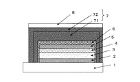
上記実施形態では、第一パッシベーション層6を1層構成で形成したが、この限りでない。図2に示すように2層構成で形成しても良い。
In the said embodiment, although the
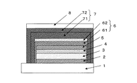
上記実施形態では、有機化合物層3、電子注入層4、上部電極5、さらには有機平坦化膜を覆うように、第一パッシべーション層6を形成したが、この限りでない。図3に示すように、第一パッシべーション層6は、上部電極5の露出面全てを覆わなくても良く、電子注入層4を覆っていれば良い。また、図4に示したように、第一パッシべーション層6を第二パッシべーション層7より露出させて形成しても良い。
In the above embodiment, the
なお、第二パッシべーション層7上に、フィルムやガラス板を粘着剤等で貼り合せることもできる。図5及び図6に示すように、第二パッシべーション層7上に直接、円偏光板8を貼り付けると、有機EL素子の厚さを薄くするのに効果的である。
Note that a film or a glass plate can be bonded to the
以下、本発明の実施例について説明する。 Examples of the present invention will be described below.
[実施例1]
図1に示す本発明の有機EL素子におけるボイドの発生について評価する。
[Example 1]
The generation of voids in the organic EL device of the present invention shown in FIG. 1 is evaluated.
図1の構成の基板1は、ガラス基板上に不図示のTFT、絶縁膜、有機平坦化膜の順で積層形成し、その上にクロムからなる下部電極2を形成し、さらにその周辺を不図示のポリイミド製素子分離膜で絶縁している。
The
まず、上記基板1を真空ベーク炉で、200℃、4時間ベークした。その後、大気圧まで戻し、真空ベーク炉から取り出して、基板を搬送した。次に、基板をベーク室に入れ、1E−4Paの真空度まで真空引きして、150℃、10分間ベークした。UV室に基板1を搬送し、UV室をドライエアーで大気圧にして、UV/オゾン洗浄を実施した。1E−4Paの真空度まで真空引きして、蒸着室に基板1を搬送した。その後の有機化合物層の蒸着工程から第二パッシべーション層7の形成完了までは、真空一貫で有機EL素子を作製した。
First, the
蒸着工程では、上記基板1のCrからなる下部電極2上に有機化合物層3を、ホール輸送層、発光層、電子輸送層の順で蒸着し、さらに電子注入層4を蒸着し、積層形成した。蒸着室は、予め材料を取り付け、1E−4Pa台まで排気されている。この蒸着室に基板を搬送した後、下部電極2上にN,N’−α−ジナフチルベンジジン(α−NPD)を40nmの膜厚となるように成膜して正孔輸送層を形成した。
The deposition process, the
その上に緑色発光することが知られたクマリン色素(1.0vol%)とトリス[8−ヒドロキシキノリナート]アルミニウム(Alq3)の共蒸着膜を30nmの膜厚になるように成膜して発光層を形成した。 A co-evaporated film of coumarin dye (1.0 vol%) and tris [8-hydroxyquinolinato] aluminum (Alq3), which is known to emit green light, is formed to a thickness of 30 nm. A light emitting layer was formed.
次に、電子輸送層として、化学式1: Next, chemical formula 1:
電子輸送層の上に、炭酸セシウム(2.9vol%)と化学式1で表されるフェナントロリン化合物の共蒸着膜を40nmの膜厚で成膜し、電子注入層4とした。
On the electron transport layer, a co-deposited film of cesium carbonate (2.9 vol%) and a phenanthroline compound represented by the
電子注入層4まで成膜した基板1を、スパッタ室へ移動させ、前記電子注入層4上にインジウム錫酸化物(ITO)をDCスパッタ法にて60nmの膜厚で成膜し、陰極5を得た。
The
別のスパッタ室へ基板1を搬送し、ターゲットに珪素材料を用い、窒素とアルゴンガスを流し、成膜圧力を0.8Paに調整して、窒化珪素をDCスパッタ法にて240nmの膜厚で成膜して、第一パッシべーション層6を得た。
The
CVD室へ基板1を搬送し、モノシランガス、亜酸化窒素ガス、窒素ガス、水素ガスをフローし、反応空間圧力を100Paに制御した。そして、60MHz高周波電力を高周波電極に供給し、膜厚を約2μmの酸化窒化シリコン膜からなる第二パッシべーション層7の第一層71を堆積形成した。
The
連続してモノシランガス、窒素ガス、水素ガスをフローし、反応空間圧力を100Paに制御した。そして、60MHz高周波電力を高周波電極に供給し、膜厚を約1μmの窒化シリコン膜からなる第二パッシべーション層7の第二層72を堆積形成した。
Monosilane gas, nitrogen gas, and hydrogen gas were continuously flowed, and the reaction space pressure was controlled to 100 Pa. Then, 60 MHz high frequency power was supplied to the high frequency electrode, and the
その後、ボイドの発生をオリンパス製光学顕微鏡(対物5倍〜20倍)で評価した。ボイドは、半球のように膨らみダークスポットとなる。ボイドサイズが大きいとパッシベーション層7に亀裂が生じ、透湿によりダークスポットは、拡大する。実施例1では、半球状の直径が2μm以上のボイドによるダークスポットは認められなかった。
Then, generation | occurrence | production of the void was evaluated with the Olympus optical microscope (
[実施例2]
実施例2では、第一パッシべーション層6に酸化珪素を用いて、図1に示す有機EL素子を第一パッシべーション層6の膜厚を変えて製作した。
[Example 2]
In Example 2, the organic EL element shown in FIG. 1 was manufactured by changing the film thickness of the
実施例1と同様の基板を用い、真空ベークから上部電極の形成までは、実施例1と同様の工程で形成した。 Using the same substrate as in Example 1, the process from vacuum baking to formation of the upper electrode was performed in the same process as in Example 1.
別のスパッタ室へ基板を搬送し、酸素とアルゴンガスを流し、成膜圧力を0.8Paに調整して、酸化珪素をDCスパッタ法にて成膜して、第一パッシべーション層6を得た。
The substrate is transported to another sputtering chamber, oxygen and argon gas are flown, the film forming pressure is adjusted to 0.8 Pa, silicon oxide is formed by DC sputtering, and the
実施例1と同様にして第二パッシべーション層7を形成した。
A
上記工程を繰返し、第一パッシべーション層6の膜厚が50nm、80nm、150nm、250nmの有機EL素子を各3枚づつ製作した。
The above steps were repeated to produce three organic EL elements each having a thickness of the
実施例1と同様にボイドの発生を光学顕微鏡(対物5〜20倍)で評価した。 In the same manner as in Example 1, the generation of voids was evaluated with an optical microscope (objective 5 to 20 times).
評価結果を表1に示す。 The evaluation results are shown in Table 1.
表1の膜厚は、第一パッシべーション層の膜厚である。 The film thickness in Table 1 is the film thickness of the first passivation layer.
ボイド径は最大のものの径を表し、2μm以上のボイド数を3枚の有機EL素子の平均数で表した。 The void diameter represents the largest diameter, and the number of voids of 2 μm or more was represented by the average number of three organic EL elements.
第一パッシべーション層6の膜厚を50nmで形成した場合は、ボイドサイズは最大15μm程度で、ボイド数は18個であった。
When the thickness of the
第一パッシべーション層6の膜厚を80nmで形成した場合は、ボイドサイズは最大10μm弱程度にまで、小さくなり、ボイド数も8個に半減した。
When the thickness of the
第一パッシべーション層6の膜厚を150nmで形成した場合は、ボイドサイズは最大5μm程度で、更に小型化し、ボイド数も4個に減少した。
When the film thickness of the
第一パッシべーション層6の膜厚を250nmで形成した場合は、ボイドサイズは2μm以下であった。
When the thickness of the
このように、第一パッシべーション層6の膜厚を80nm以上に厚くすると効果が大きい結果が得られた。また、第一パッシベーション層6の膜厚を250nmで形成した場合は、2μm以上のボイドは認められなかった。
As described above, a large effect was obtained when the thickness of the
[実施例3]
実施例3では、第一パッシべーション層6の第一層61に酸化珪素を用い、第二層62に窒化珪素を用いて、図2に示す有機EL素子を膜厚を変えて製作した。
[Example 3]
In Example 3, the
実施例1と同様の基板1を用い、真空ベークから上部電極2の形成までは、実施例1と同様の工程で形成した。
The
別のスパッタ室へ基板1を搬送し、珪素からなるターゲットを用い、酸素とアルゴンガスを流し、成膜圧力を0.8Paに調整して、酸化珪素をDCスパッタ法にて成膜し、第一パッシべーション層6の第一層61を得た。
The
別のスパッタ室へ基板1を搬送し、珪素からなるターゲットを用い、窒素とアルゴンガスを流し、成膜圧力を0.7Paに調整して、窒化珪素をDCスパッタ法にて成膜し、第一パッシべーション層6の第二層62を得た。
The
実施例1と同様にして第二パッシべーション層7を形成した。
A
上記工程を繰返し、実施例2と同様に各3枚の有機EL素子を製作した。 The above process was repeated to produce three organic EL elements each in the same manner as in Example 2.
実施例1と同様にボイドの発生を光学顕微鏡で評価した。評価結果を表2に示す。 In the same manner as in Example 1, the generation of voids was evaluated with an optical microscope. The evaluation results are shown in Table 2.
表2の膜厚は、第一パッシべーション層の第一層、第二層の膜厚である。 The film thicknesses in Table 2 are the film thicknesses of the first and second layers of the first passivation layer.
第一パッシべーション層6の第一層61の膜厚を50nm、第一パッシべーション層6の第二層62の膜厚を50nmで形成した場合は、ボイドサイズは最大10μmを下回り、ボイド数は5個であった。
When the film thickness of the
第一パッシべーション層6の第一層61の膜厚を80nm、第一パッシべーション層6の第二層62の膜厚を50nmで形成した場合は、ボイドサイズは最大3μm程度にまで小さくなり、ボイド数も2個に半減した。
When the
第一パッシべーション層6の第一層61の膜厚を150nm、第一パッシべーション層6の第二層62の膜厚を50nmで形成した場合は、2μm以上のボイドは認められなかった。
When the film thickness of the
第一パッシべーション層6の第一層61の膜厚を250nm、第一パッシべーション層6の第二層62の膜厚を50nmで形成した場合も、ボイドは認められかった。
No voids were observed when the
このように、第一パッシべーション層6の第二層62を窒化珪素で積層するとボイドが大幅に減少する大きな効果が得られた。また、第一パッシべーション層6の積層膜厚200nm以上では、ボイドが認められなかった。
As described above, when the
[実施例4]
実施例4では、第一パッシべーション層6に窒化珪素を用いて、図1に示す有機EL素子を膜厚を変えて製作した。
[Example 4]
In Example 4, the
実施例1と同様の基板を用い、真空ベークから上部電極5の形成までは、実施例1と同様の工程で形成した。
The same substrate as in Example 1 was used, and the process from vacuum baking to formation of the
実施例4では真空通い箱を用い、イオンビームスパッタ装置へ基板1を搬送し、窒素ガスを流し、窒化珪素をイオンビームスパッタ法にて成膜して、第一パッシべーション層6を得た。
In Example 4, a vacuum pass box was used, the
その後、再度真空通い箱を用いてCVD室へ基板1を搬送し、モノシランガス、アンモニアガス、窒素ガスをフローし、反応空間圧力を100Paに制御した。そして、60MHz高周波電力を高周波電極に供給し、膜厚を約2μmの窒化シリコン膜からなる第二パッシべーション層7の第一層71を堆積形成した。
Thereafter, the
連続してモノシランガス、窒素ガス、水素ガスをフローし、反応空間圧力を100Paに制御した。そして、60MHz高周波電力を高周波電極に供給し、膜厚を約1μmの窒化シリコン膜からなる第二パッシべーション層7の第二層72を堆積形成した。
Monosilane gas, nitrogen gas, and hydrogen gas were continuously flowed, and the reaction space pressure was controlled to 100 Pa. Then, 60 MHz high frequency power was supplied to the high frequency electrode, and the
同様に、上記工程を繰返し、実施例2と同様に各3枚の有機EL素子を製作した。 Similarly, the above steps were repeated, and three organic EL elements were produced in the same manner as in Example 2.
実施例1と同様にボイドの発生を光学顕微鏡で評価した。評価結果を表3に示す。 In the same manner as in Example 1, the generation of voids was evaluated with an optical microscope. The evaluation results are shown in Table 3.
表3の膜厚は、第一パッシべーション層の膜厚である。 The film thickness in Table 3 is the film thickness of the first passivation layer.
第一パッシべーション層6の膜厚を50nmで形成した場合は、ボイドサイズは最大15μm程度で、ボイド数は17個であった。
When the thickness of the
第一パッシべーション層6の膜厚を80nmで形成した場合は、ボイドサイズは最大8μm強程度にまで、小さくなり、ボイド数も6個に減少した。
When the
第一パッシべーション層6の膜厚を150nmで形成した場合は、ボイドサイズは最大3μm程度で、更に小型可し、ボイド数も2個に減少した。
When the film thickness of the
第一パッシべーション層6の膜厚を250nmで形成した場合は、2μm以上のボイドは認められなかった。
When the film thickness of the
このように、第二パッシべーション層7を窒化珪素で形成するとボイド数は減少する。更に、第二パッシベーション層7の膜厚が80nm以上では、ボイドが大幅に減少する大きな効果が得られた。
Thus, the number of voids decreases when the
[実施例5]
実施例5では、図6に示す有機EL素子を製作した。
[Example 5]
In Example 5, the organic EL element shown in FIG. 6 was manufactured.
実施例1と同様の基板を用い、真空ベークから上部電極2の形成までは、実施例1と同様の工程で形成した。
The same substrate as in Example 1 was used, and the process from vacuum baking to formation of the
真空通い箱を用い、イオンビームスパッタ装置へ基板を搬送し、酸素ガスを流し酸化珪素をイオンビームスパッタ法にて成膜して、膜厚100nmの第一パッシべーション層6の第一層61を得た。次に、基板1を退避させ、窒素ガスを流してプレスパッタを行った後、基板1をイオンビームスパッタ装置へ投入した。続けて窒素ガスを流し、窒化珪素をイオンビームスパッタ法にて成膜して、膜厚150nmの第一パッシべーション層6の第二層62を得た。
Using a vacuum pass box, the substrate is transferred to an ion beam sputtering apparatus, oxygen gas is flown and silicon oxide is deposited by ion beam sputtering, and the
その後、真空通い箱を用い、真空紫外光CVD装置へ基板1を搬送した。そして、真空紫外光CVD法にてポリシロキサンのOMCTSを材料ガスに用いて、膜厚約2μmの酸化珪素がベースでSi−CH3も多く含まれる第二パッシべーション層7の第一層71を堆積形成した。
Then, the board |
プラズマCVD室へ基板1を搬送した。そして、モノシランガス、窒素ガス、水素ガスをフローし、反応空間圧力を100Paに制御した。次に、60MHz高周波電力を高周波電極に供給し、膜厚を約1μmの窒化シリコン膜からなる第二パッシべーション層7の第二層72を堆積形成した。
The
その後、パッシべーション層の上に円偏光板8を貼り付けた。
Then, the circularly-polarizing
有機EL素子の初期輝度特性を測定した。 The initial luminance characteristics of the organic EL element were measured.
実施例1と同様にボイドの発生を光学顕微鏡で評価した。また、輝度特性を測定した。 In the same manner as in Example 1, the generation of voids was evaluated with an optical microscope. In addition, luminance characteristics were measured.
ボイドサイズは最大2μm弱程度であった。 The maximum void size was a little less than 2 μm.
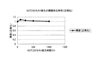
続けて、60℃90%RHの恒温恒湿槽に入れ、トータル96時間後、250時間後、500時間後、1000時間後の輝度測定とダークスポットの発生と輝度特性を評価した。輝度特性の結果を図7に示す。 Subsequently, the sample was placed in a constant temperature and humidity chamber at 60 ° C. and 90% RH, and the luminance measurement, generation of dark spots, and luminance characteristics were evaluated after 96 hours, 250 hours, 500 hours, and 1000 hours. The result of the luminance characteristic is shown in FIG.
60℃90%RH、1000時間後においても、3μmを越えるダークスポットは発生しなかった。輝度特性劣化においても、初期輝度の101%で劣化は無かった。 Even after 1000 hours at 60 ° C. and 90% RH, no dark spot exceeding 3 μm was generated. Even in the luminance characteristic deterioration, there was no deterioration at 101% of the initial luminance.
[実施例6]
実施例6では、図5に示す有機EL素子を製作した。
[Example 6]
In Example 6, the organic EL element shown in FIG. 5 was manufactured.
実施例1と同様の基板を用い、真空ベークから上部電極の形成までは、実施例1と同様の工程で形成した。 Using the same substrate as in Example 1, the process from vacuum baking to formation of the upper electrode was performed in the same process as in Example 1.
次に、イオンビームスパッタ装置へ基板1を搬送し、窒素ガスを流し、窒化珪素をイオンビームスパッタ法にて成膜して、膜厚250nmの第一パッシべーション層6を得た。
Next, the
その後、実施例5と同様に、真空紫外光CVD装置へ基板1を搬送した。そして、真空紫外光CVD法にてポリシロキサンのOMCTSを材料ガスに用いて、膜厚約2μmの酸化珪素がベースでSi−CH3も含まれる第二パッシべーション層7の第一層71を堆積形成した。
Thereafter, as in Example 5, the
イオンビームスパッタ装置へ基板1を搬送し、窒素ガスを流し、窒化珪素をイオンビームスパッタ法にて成膜して、膜厚250nmからなる第二パッシべーション層7の第二層72を堆積形成した。
The
その後、パッシべーション層の上に円偏光板8を貼り付けた。
Then, the circularly-polarizing
実施例1と同様にボイドの発生を光学顕微鏡で評価した。 In the same manner as in Example 1, the generation of voids was evaluated with an optical microscope.
直径2μmを越えるボイドは見当たらなかった。 There were no voids exceeding 2 μm in diameter.
続けて、60℃90%RHの恒温恒湿槽に入れ、トータル1000時間後の輝度測定とダークスポットの発生を評価した。 Subsequently, the sample was placed in a constant temperature and humidity chamber at 60 ° C. and 90% RH, and luminance measurement after 1000 hours in total and generation of dark spots were evaluated.
60℃90%RH、1000時間後においても、3μmを越えるダークスポットは発生しなかった。輝度特性劣化においても、初期輝度の102%で劣化は無かった。 Even after 1000 hours at 60 ° C. and 90% RH, no dark spot exceeding 3 μm was generated. Even in the luminance characteristic deterioration, there was no deterioration at 102% of the initial luminance.
[実施例7]
実施例7では、図6に示す有機EL素子を製作した。
[Example 7]
In Example 7, the organic EL element shown in FIG. 6 was manufactured.
実施例1と同様の基板を用い、真空ベークから上部電極の形成までは、実施例1と同様の工程で形成した。 Using the same substrate as in Example 1, the process from vacuum baking to formation of the upper electrode was performed in the same process as in Example 1.
次に、蒸着装置へ基板を搬送し、酸化珪素をEB蒸着法にて成膜して、膜厚100nmの第一パッシべーション層6の第一層61を得た。さらにイオンビームスパッタ装置に基板を搬送し、窒化珪素をイオンビームスパッタ法にて成膜して、膜厚100nmの第一パッシべーション層6の第二層62を得た。
Next, the substrate was transported to a vapor deposition apparatus, and silicon oxide was deposited by EB vapor deposition to obtain a
その後、ラジカルシャワーCVD装置へ基板を搬送し、ラジカルシャワーCVD法にてモノシランガスとアンモニアガスを材料ガスに用いて、膜厚約2μmの窒化珪素からなる第二パッシべーション層7の第一層71を堆積形成した。
Thereafter, the substrate is transported to a radical shower CVD apparatus, and the
Cat−CVD装置へ基板を移動し、モノシランガス、アンモニアガス、水素ガスをフローし、膜厚を約1μmの窒化シリコン膜からなる第二パッシべーション層7の第二層72を堆積形成した。
The substrate was moved to a Cat-CVD apparatus, and monosilane gas, ammonia gas, and hydrogen gas were flowed to deposit and form a
その後、パッシべーション層の上に円偏光板8を貼り付けた。
Then, the circularly-polarizing
実施例1と同様にボイドの発生を光学顕微鏡で評価した。 In the same manner as in Example 1, the generation of voids was evaluated with an optical microscope.
2μm以上のボイドは見当たらなかった。 There were no voids of 2 μm or more.
続けて、60℃90%RHの恒温恒湿槽に入れ、トータル1000時間後の輝度測定とダークスポットの発生を評価した。 Subsequently, the sample was placed in a constant temperature and humidity chamber at 60 ° C. and 90% RH, and luminance measurement after 1000 hours in total and generation of dark spots were evaluated.
60℃90%RH、1000時間後においても、3μmを越えるダークスポットは発生しなかった。輝度特性劣化においても、初期輝度の99%で劣化は無かった。 Even after 1000 hours at 60 ° C. and 90% RH, no dark spot exceeding 3 μm was generated. Even in the luminance characteristic deterioration, there was no deterioration at 99% of the initial luminance.
[比較例]
比較例では、図8に示す第一パッシべーション層6を用いない有機EL素子を製作した。
[Comparative example]
In the comparative example, an organic EL element not using the
実施例1と同様の基板1を用い、真空ベークから上部電極2の形成までは、実施例1と同様の工程で形成した。
The
第一パッシべーション層6を形成しないで、プラズマCVD室へ基板を搬送した。
The substrate was transferred to the plasma CVD chamber without forming the
その後、モノシランガス、亜酸化窒素ガス、窒素ガス、水素ガスをフローし、反応空間圧力を100Paに制御した。そして、60MHz高周波電力を高周波電極に供給し、膜厚を約2μmの酸化窒化シリコン膜からなる第二パッシべーション層7の第一層71を堆積形成した。
Thereafter, monosilane gas, nitrous oxide gas, nitrogen gas, and hydrogen gas were flowed, and the reaction space pressure was controlled to 100 Pa. Then, 60 MHz high frequency power was supplied to the high frequency electrode, and the
さらに、モノシランガス、窒素ガス、水素ガスをフローし、成膜圧力を100Paに制御し、膜厚約1μmの窒化シリコン膜からなる第二パッシべーション層7の第二層72をプラズマCVD法にて堆積形成した。
Further, a monosilane gas, a nitrogen gas, and a hydrogen gas are flowed, the film forming pressure is controlled to 100 Pa, and the
第二パッシべーション層7の上に円偏光板8を貼り付けた。
A circularly
実施例1と同様にボイドの発生を光学顕微鏡で評価した。 In the same manner as in Example 1, the generation of voids was evaluated with an optical microscope.
ボイドサイズは最大20μm程度で、ボイドは38個に達した。また、膜が割れて剥れているボイドも発生した。 The maximum void size was about 20 μm, and the number of voids reached 38. Moreover, the void which the film | membrane cracked and peeled also generate | occur | produced.
上部電極の上に第一パッシべーション層6を形成した場合に比べ、ボイド数は、2倍に増加した。
Compared with the case where the
発光させて、ダークスポットを調べると、38箇所のボイド部は、3μm以上のダークスポットとなっていた。 When the dark spots were examined by emitting light, 38 void portions were dark spots of 3 μm or more.
1 基板
2 下部電極
3 有機化合物層(ホール注入層/発光層/電子輸送層)
4 電子注入層
5 上部電極
6 第一パッシべーション層
7 第二パッシべーション層
8 円偏光板
61 第一パッシべーション層の第一層
62 第一パッシべーション層の第二層
71 第二パッシべーション層の第一層
72 第二パッシべーション層の第二層
1
4
Claims (4)
前記有機化合物層のうち電子注入層がアルカリ金属又はアルカリ金属化合物を含有し、前記上部電極は酸化膜からなり、
前記積層する工程は、前記電子注入層を形成する工程と、前記電子注入層の直上に前記上部電極を形成する工程とを含み、
前記パッシベーション層を形成する工程は、前記上部電極の直上に珪素を含みかつ水素を含まない材料を用いて第一パッシベーション層を形成する工程と、前記第一パッシベーション層の上に珪素および水素を含む材料を用いて、CVD法により第二パッシベーション層を形成する工程とを含むことを特徴とする有機EL素子の製造方法。 A step of laminating a lower electrode and the organic compound layer and the upper portion electrode on the substrate, and forming a passivation layer covering them, in the manufacturing method of the organic EL element having at least,
Of the organic compound layer, the electron injection layer contains an alkali metal or an alkali metal compound, and the upper electrode is made of an oxide film,
The step of laminating includes a step of forming the electron injection layer, and a step of forming the upper electrode directly on the electron injection layer,
The step of forming the passivation layer includes a step of forming a first passivation layer using a material that contains silicon and does not contain hydrogen immediately above the upper electrode, and includes silicon and hydrogen on the first passivation layer. Forming a second passivation layer by a CVD method using a material, and a method for manufacturing an organic EL element.
Priority Applications (2)
| Application Number | Priority Date | Filing Date | Title |
|---|---|---|---|
| JP2007220813A JP5241173B2 (en) | 2007-08-28 | 2007-08-28 | Manufacturing method of organic EL element |
| US12/193,620 US7994707B2 (en) | 2007-08-28 | 2008-08-18 | Organic el device and method of producing the device |
Applications Claiming Priority (1)
| Application Number | Priority Date | Filing Date | Title |
|---|---|---|---|
| JP2007220813A JP5241173B2 (en) | 2007-08-28 | 2007-08-28 | Manufacturing method of organic EL element |
Publications (3)
| Publication Number | Publication Date |
|---|---|
| JP2009054444A JP2009054444A (en) | 2009-03-12 |
| JP2009054444A5 JP2009054444A5 (en) | 2010-10-14 |
| JP5241173B2 true JP5241173B2 (en) | 2013-07-17 |
Family
ID=40406365
Family Applications (1)
| Application Number | Title | Priority Date | Filing Date |
|---|---|---|---|
| JP2007220813A Expired - Fee Related JP5241173B2 (en) | 2007-08-28 | 2007-08-28 | Manufacturing method of organic EL element |
Country Status (2)
| Country | Link |
|---|---|
| US (1) | US7994707B2 (en) |
| JP (1) | JP5241173B2 (en) |
Families Citing this family (9)
| Publication number | Priority date | Publication date | Assignee | Title |
|---|---|---|---|---|
| KR100999779B1 (en) * | 2010-02-01 | 2010-12-08 | 엘지이노텍 주식회사 | Light emitting device, manufacturing method and light emitting device package |
| TWI515936B (en) * | 2011-12-15 | 2016-01-01 | 友達光電股份有限公司 | Light emitting device and manufacturing method thereof |
| KR101980231B1 (en) * | 2012-09-18 | 2019-05-21 | 삼성디스플레이 주식회사 | Flat display device including thin film encapsulation and the manufacturing method thereof |
| JP2014141714A (en) * | 2013-01-24 | 2014-08-07 | Kaneka Corp | Manufacturing method of vacuum evaporation system and organic el apparatus |
| WO2015170657A1 (en) * | 2014-05-07 | 2015-11-12 | シャープ株式会社 | Electroluminescent device and method for producing same |
| JP6586328B2 (en) * | 2015-09-04 | 2019-10-02 | 東京エレクトロン株式会社 | Method for processing an object |
| CN105552247B (en) * | 2015-12-08 | 2018-10-26 | 上海天马微电子有限公司 | Composite substrate, flexible display device and preparation method thereof |
| KR102125204B1 (en) * | 2018-10-05 | 2020-06-22 | 경희대학교 산학협력단 | Thin-film light emitting device comprising charge electron transport layer and manufacturing method thereof |
| CN113748528B (en) | 2020-03-27 | 2023-04-11 | 京东方科技集团股份有限公司 | Display substrate, preparation method thereof and display device |
Family Cites Families (10)
| Publication number | Priority date | Publication date | Assignee | Title |
|---|---|---|---|---|
| JP2000077183A (en) | 1998-08-31 | 2000-03-14 | Pioneer Electronic Corp | Method for manufacturing organic electroluminescent device |
| JP3817081B2 (en) * | 1999-01-29 | 2006-08-30 | パイオニア株式会社 | Manufacturing method of organic EL element |
| US7339317B2 (en) * | 2000-06-05 | 2008-03-04 | Semiconductor Energy Laboratory Co., Ltd. | Light-emitting device having triplet and singlet compound in light-emitting layers |
| JP4600857B2 (en) | 2000-10-27 | 2010-12-22 | Tdk株式会社 | Organic EL device manufacturing method and organic EL device |
| JP3705282B2 (en) * | 2002-10-03 | 2005-10-12 | セイコーエプソン株式会社 | DISPLAY PANEL, ELECTRONIC DEVICE HAVING THE DISPLAY PANEL, AND DISPLAY PANEL MANUFACTURING METHOD |
| JP4588312B2 (en) * | 2003-12-02 | 2010-12-01 | 株式会社半導体エネルギー研究所 | Method for manufacturing light emitting device |
| JP2005203321A (en) * | 2004-01-19 | 2005-07-28 | Pioneer Electronic Corp | Protective film and organic el device |
| KR100699988B1 (en) * | 2004-03-19 | 2007-03-26 | 삼성에스디아이 주식회사 | Flat Panel Display |
| JP2005322464A (en) * | 2004-05-07 | 2005-11-17 | Canon Inc | Organic EL device |
| JP5268249B2 (en) * | 2005-12-14 | 2013-08-21 | キヤノン株式会社 | Manufacturing method of organic light emitting device |
-
2007
- 2007-08-28 JP JP2007220813A patent/JP5241173B2/en not_active Expired - Fee Related
-
2008
- 2008-08-18 US US12/193,620 patent/US7994707B2/en active Active
Also Published As
| Publication number | Publication date |
|---|---|
| US20090058275A1 (en) | 2009-03-05 |
| JP2009054444A (en) | 2009-03-12 |
| US7994707B2 (en) | 2011-08-09 |
Similar Documents
| Publication | Publication Date | Title |
|---|---|---|
| JP5241173B2 (en) | Manufacturing method of organic EL element | |
| US8638032B2 (en) | Organic optoelectronic device coated with a multilayer encapsulation structure and a method for encapsulating said device | |
| KR101366449B1 (en) | Optical semiconductor device and manufaturing method thereof | |
| US20110097533A1 (en) | Thin film encapsulation method | |
| US20160056414A1 (en) | Thin film permeation barrier system for substrates and devices and method of making the same | |
| TW200913344A (en) | Method for applying a thin-film encapsulation layer assembly to an organic device, and an organic device provided with a thin-film encapsulation layer assembly preferably applied with such a method | |
| US8975534B2 (en) | Flexible base material and flexible electronic device | |
| CN100433403C (en) | Organic electroluminescent device and method of manufacturing the same | |
| CN104051652B (en) | A kind of flexible thin-film transistor | |
| TW200934284A (en) | Organic electroluminescence display device and manufacturing method thereof | |
| US9281420B2 (en) | Chemical vapor deposited film formed by plasma CVD method | |
| US20140264296A1 (en) | Barrier film performance with n2o dilution process for thin film encapsulation | |
| US20170117503A1 (en) | Buffer layer for organic light emitting devices and method of making the same | |
| CN104160062B (en) | Silicon-containing film and silicon-containing film forming method | |
| JP2005166400A (en) | Surface protective film | |
| US8487413B2 (en) | Passivation film for electronic device and method of manufacturing the same | |
| KR102375255B1 (en) | Film for preventing humidity from percolation and Method for manufacturing the same | |
| JP5049613B2 (en) | Organic light emitting device and manufacturing method thereof | |
| CN115036332A (en) | Array substrate, preparation method thereof and display panel | |
| KR20150014053A (en) | Method of fabricating the organic light emitting diode display device | |
| WO2015061656A1 (en) | Flexible permation barrier system deposited in a single process and having ultralow permeability and low mechanical stress over its service life | |
| KR100953372B1 (en) | Method of gas barrier layer formation using low temperature curing and method for manufacturing organic light emitting display using the same | |
| CN120981104A (en) | A silicon-based OLED packaging structure and fabrication method, and a display panel. | |
| WO2014147789A1 (en) | Organic electroluminescence device, organic electroluminescence device manufacturing method, and film forming method |
Legal Events
| Date | Code | Title | Description |
|---|---|---|---|
| A521 | Request for written amendment filed |
Free format text: JAPANESE INTERMEDIATE CODE: A523 Effective date: 20100827 |
|
| A621 | Written request for application examination |
Free format text: JAPANESE INTERMEDIATE CODE: A621 Effective date: 20100827 |
|
| A977 | Report on retrieval |
Free format text: JAPANESE INTERMEDIATE CODE: A971007 Effective date: 20111222 |
|
| A131 | Notification of reasons for refusal |
Free format text: JAPANESE INTERMEDIATE CODE: A131 Effective date: 20111227 |
|
| A521 | Request for written amendment filed |
Free format text: JAPANESE INTERMEDIATE CODE: A523 Effective date: 20120224 |
|
| A131 | Notification of reasons for refusal |
Free format text: JAPANESE INTERMEDIATE CODE: A131 Effective date: 20120619 |
|
| TRDD | Decision of grant or rejection written | ||
| A01 | Written decision to grant a patent or to grant a registration (utility model) |
Free format text: JAPANESE INTERMEDIATE CODE: A01 Effective date: 20130305 |
|
| A61 | First payment of annual fees (during grant procedure) |
Free format text: JAPANESE INTERMEDIATE CODE: A61 Effective date: 20130402 |
|
| FPAY | Renewal fee payment (event date is renewal date of database) |
Free format text: PAYMENT UNTIL: 20160412 Year of fee payment: 3 |
|
| R151 | Written notification of patent or utility model registration |
Ref document number: 5241173 Country of ref document: JP Free format text: JAPANESE INTERMEDIATE CODE: R151 |
|
| FPAY | Renewal fee payment (event date is renewal date of database) |
Free format text: PAYMENT UNTIL: 20160412 Year of fee payment: 3 |
|
| LAPS | Cancellation because of no payment of annual fees |