JP5226669B2 - High-efficiency flash memory data transfer - Google Patents
High-efficiency flash memory data transfer Download PDFInfo
- Publication number
- JP5226669B2 JP5226669B2 JP2009507905A JP2009507905A JP5226669B2 JP 5226669 B2 JP5226669 B2 JP 5226669B2 JP 2009507905 A JP2009507905 A JP 2009507905A JP 2009507905 A JP2009507905 A JP 2009507905A JP 5226669 B2 JP5226669 B2 JP 5226669B2
- Authority
- JP
- Japan
- Prior art keywords
- controller
- data
- flash memory
- enable signal
- input
- Prior art date
- Legal status (The legal status is an assumption and is not a legal conclusion. Google has not performed a legal analysis and makes no representation as to the accuracy of the status listed.)
- Active
Links
- 238000012546 transfer Methods 0.000 title claims description 245
- 230000015654 memory Effects 0.000 title claims description 147
- 238000000034 method Methods 0.000 claims description 122
- 230000007704 transition Effects 0.000 claims description 50
- 230000004044 response Effects 0.000 claims description 32
- 230000005540 biological transmission Effects 0.000 claims description 17
- 238000004070 electrodeposition Methods 0.000 claims 1
- 230000008569 process Effects 0.000 description 92
- 240000007320 Pinus strobus Species 0.000 description 78
- 230000000630 rising effect Effects 0.000 description 28
- 238000010586 diagram Methods 0.000 description 25
- 230000006854 communication Effects 0.000 description 18
- 238000004891 communication Methods 0.000 description 18
- 230000001360 synchronised effect Effects 0.000 description 15
- 238000013459 approach Methods 0.000 description 13
- 239000004020 conductor Substances 0.000 description 10
- 230000003111 delayed effect Effects 0.000 description 5
- 238000005516 engineering process Methods 0.000 description 5
- 230000009467 reduction Effects 0.000 description 5
- 230000009286 beneficial effect Effects 0.000 description 4
- 230000008901 benefit Effects 0.000 description 4
- 230000002457 bidirectional effect Effects 0.000 description 4
- 230000006870 function Effects 0.000 description 4
- 230000006872 improvement Effects 0.000 description 4
- 230000004048 modification Effects 0.000 description 4
- 238000012986 modification Methods 0.000 description 4
- 239000004065 semiconductor Substances 0.000 description 4
- 230000001934 delay Effects 0.000 description 3
- 239000007787 solid Substances 0.000 description 3
- 239000003795 chemical substances by application Substances 0.000 description 2
- 230000000295 complement effect Effects 0.000 description 2
- 238000013500 data storage Methods 0.000 description 2
- 230000001419 dependent effect Effects 0.000 description 2
- 230000000694 effects Effects 0.000 description 2
- 230000000977 initiatory effect Effects 0.000 description 2
- 208000033748 Device issues Diseases 0.000 description 1
- 102100034004 Gamma-adducin Human genes 0.000 description 1
- 101000799011 Homo sapiens Gamma-adducin Proteins 0.000 description 1
- 108010076504 Protein Sorting Signals Proteins 0.000 description 1
- 230000007175 bidirectional communication Effects 0.000 description 1
- 230000001413 cellular effect Effects 0.000 description 1
- 230000002860 competitive effect Effects 0.000 description 1
- 238000013461 design Methods 0.000 description 1
- 238000007667 floating Methods 0.000 description 1
- 230000017525 heat dissipation Effects 0.000 description 1
- 230000014759 maintenance of location Effects 0.000 description 1
- 238000007726 management method Methods 0.000 description 1
- 229910044991 metal oxide Inorganic materials 0.000 description 1
- 150000004706 metal oxides Chemical class 0.000 description 1
- 230000003071 parasitic effect Effects 0.000 description 1
- 230000002093 peripheral effect Effects 0.000 description 1
- 238000006467 substitution reaction Methods 0.000 description 1
Images


Classifications
-
- G—PHYSICS
- G11—INFORMATION STORAGE
- G11C—STATIC STORES
- G11C7/00—Arrangements for writing information into, or reading information out from, a digital store
- G11C7/10—Input/output [I/O] data interface arrangements, e.g. I/O data control circuits, I/O data buffers
- G11C7/1015—Read-write modes for single port memories, i.e. having either a random port or a serial port
- G11C7/1045—Read-write mode select circuits
-
- G—PHYSICS
- G11—INFORMATION STORAGE
- G11C—STATIC STORES
- G11C7/00—Arrangements for writing information into, or reading information out from, a digital store
- G11C7/10—Input/output [I/O] data interface arrangements, e.g. I/O data control circuits, I/O data buffers
- G11C7/1051—Data output circuits, e.g. read-out amplifiers, data output buffers, data output registers, data output level conversion circuits
- G11C7/1066—Output synchronization
-
- G—PHYSICS
- G11—INFORMATION STORAGE
- G11C—STATIC STORES
- G11C7/00—Arrangements for writing information into, or reading information out from, a digital store
- G11C7/10—Input/output [I/O] data interface arrangements, e.g. I/O data control circuits, I/O data buffers
- G11C7/1078—Data input circuits, e.g. write amplifiers, data input buffers, data input registers, data input level conversion circuits
- G11C7/1093—Input synchronization
-
- G—PHYSICS
- G11—INFORMATION STORAGE
- G11C—STATIC STORES
- G11C7/00—Arrangements for writing information into, or reading information out from, a digital store
- G11C7/20—Memory cell initialisation circuits, e.g. when powering up or down, memory clear, latent image memory
-
- G—PHYSICS
- G11—INFORMATION STORAGE
- G11C—STATIC STORES
- G11C7/00—Arrangements for writing information into, or reading information out from, a digital store
- G11C7/22—Read-write [R-W] timing or clocking circuits; Read-write [R-W] control signal generators or management
-
- G—PHYSICS
- G11—INFORMATION STORAGE
- G11C—STATIC STORES
- G11C16/00—Erasable programmable read-only memories
- G11C16/02—Erasable programmable read-only memories electrically programmable
- G11C16/06—Auxiliary circuits, e.g. for writing into memory
- G11C16/26—Sensing or reading circuits; Data output circuits
Description
本発明は、フラッシュメモリ装置の分野に属し、特に電子システムにおけるフラッシュメモリ装置とメモリコントローラとの間のデータ通信に向けられている。 The present invention belongs to the field of flash memory devices and is particularly directed to data communication between a flash memory device and a memory controller in an electronic system.
当該技術分野で良く知られているように、“フラッシュ”メモリは、以前の電気的に消去可能でプログラム可能な読み出し専用メモリ(EEPROM)装置のようにチップ全体または大ブロックベースにではなくて、割合に小さなブロックを単位として消去および再書き込みできる電気的に消去可能な半導体メモリ装置である。このような事情で、フラッシュメモリは、記憶されているデータの不揮発性(すなわち、電源が除去された後のデータ保持)が非常に重要であるが再書き込みの頻度が割合に低い用途のために特にポピュラーになっている。フラッシュメモリのポピュラーな用途の例は、携帯用オーディオプレーヤ、携帯電話ハンドセットにおける電話番号および電話アクティビティの“SIM”カード記憶、コンピュータおよびワークステーションのための“サムキー(thumbkey)”取り外し可能な記憶装置、デジタルカメラ用の記憶装置などを含む。 As is well known in the art, “flash” memory is not on an entire chip or large block basis like previous electrically erasable and programmable read only memory (EEPROM) devices, It is an electrically erasable semiconductor memory device that can be erased and rewritten in units of relatively small blocks. In such circumstances, flash memory is used for applications in which the non-volatility of stored data (that is, data retention after the power supply is removed) is very important, but the frequency of rewriting is relatively low. It has become particularly popular. Examples of popular uses of flash memory are portable audio players, “SIM” card storage of phone numbers and phone activity in mobile phone handsets, “thumbkey” removable storage for computers and workstations, Includes storage devices for digital cameras.
半導体不揮発性メモリ技術における最近の重要な進歩は、“NOR”メモリではなくて“NAND”メモリとしてのフラッシュメモリセルの構成である。当該技術分野で知られているように、NORフラッシュメモリは、ビット線とソース線との間における平行な複数のメモリセルの列の在来の配列を指す。NOR列内の特定のセルのアクセスは、ビット線とソース線との間の電流がアクセスされたセルの状態により決定されるように、その列内の他のセルをオフに保ちながら、そのワード線(コントロールゲート)をアクティブに駆動することによって、行われる。一方、NANDメモリの列内のメモリセルは、ビット線とソース線との間に直列に接続されている。従って、NAND列内の特定のセルのアクセスは、この場合にもアクセスされたセルの状態によってビット線とソース線との間の電流が決定されるように、アクティブなワード線レベルでその列内の全てのセルをオンに転換させ、そしてアクセスされるべきセルに中間ワード線レベルを印加することを必要とする。当該技術分野で良く知られているように、NANDフラッシュメモリのビットあたりに必要なチップ面積はNORフラッシュメモリのビットあたりの面積から遥かに低減されている。その理由は、主として、NORメモリと比べてNANDメモリの列に必要とされる導体(従って、接点)が少ないこと、また、NAND構成においてアクセストランジスタが多数のセルの間で共有され得ることにある。さらに、在来のNANDフラッシュメモリは、NORメモリの場合のようにランダムアクセスメモリとしてではなくて、例えば列に沿ってセルに逐次アクセスすることによって便利に連続してアクセスされる。従って、NANDメモリは音楽およびビデオ記憶の用途に特に良く適している。 A recent significant advance in semiconductor non-volatile memory technology is the configuration of flash memory cells as “NAND” memory rather than “NOR” memory. As is known in the art, NOR flash memory refers to a conventional array of columns of parallel memory cells between a bit line and a source line. The access of a particular cell in a NOR column is the word while keeping the other cells in that column off so that the current between the bit line and the source line is determined by the state of the accessed cell. This is done by actively driving the line (control gate). On the other hand, the memory cells in the NAND memory column are connected in series between the bit line and the source line. Thus, access to a particular cell in a NAND column is again within that column at the active word line level so that the current between the bit line and source line is again determined by the state of the accessed cell. It is necessary to turn on all of the cells and apply an intermediate word line level to the cells to be accessed. As is well known in the art, the chip area required per bit of NAND flash memory is much reduced from the area per bit of NOR flash memory. The reason is mainly that fewer conductors (and therefore contacts) are required for a column of NAND memory than a NOR memory, and that an access transistor can be shared between multiple cells in a NAND configuration. . Furthermore, conventional NAND flash memory is conveniently and continuously accessed by sequentially accessing cells, for example along a column, rather than as a random access memory as in a NOR memory. Therefore, NAND memory is particularly well suited for music and video storage applications.
フラッシュメモリの分野における他の1つの重要な最近の進歩は、当該技術分野でマルチレベルプログラムセル(MLC)と称されている。このアプローチによると、単にセルのプログラミングをより精密に制御することによって、各メモリセルについて3つ以上のデータ状態が可能にされる。在来のバイナリデータ記憶では、各メモリセルは“0”状態または“1”状態にプログラムされる。このようなバイナリセルの読み出しは、アドレス指定されたメモリセルのコントロールゲートに単一の制御電圧を印加することによって成し遂げられるので、トランジスタは、“1”状態にプログラムされていれば導通するが、“0”状態ではオフに留まり、従って、アドレス指定されたメモリセルを通しての導通の感知は、セルのプログラムされた状態を報告する。対照的に、MLCアプローチの典型的な例によると、一般的にバイナリ値00,01,10,11に対応する4つの可能な状態が各メモリセルについて定められる。実際上、2つの中間の状態は、完全に消去された状態と完全にプログラムされた状態との間のセルの2つの部分的プログラミングのレベルに対応する。セルあたりに8個に及ぶ可能な状態、すなわち3個のバイナリビットを有するMLCフラッシュメモリの実施例が知られている。各メモリセルに2ビットまたは3ビットのデータを格納する能力は、フラッシュメモリチップのデータ容量を即座に2倍または3倍にする。MLCフラッシュメモリセルと、このようなMLCセルを含むメモリとの例が、米国特許第5,172,338号(特許文献1)および第6,747,892号(特許文献2)に記載されている。これら特許は両方とも、本願とともに通例譲渡され、本願明細書において参照により援用されている。
Another important recent advance in the field of flash memory is referred to in the art as multi-level program cells (MLCs). According to this approach, more than two data states are allowed for each memory cell by simply controlling the programming of the cell more precisely. In conventional binary data storage, each memory cell is programmed to a “0” state or a “1” state. Such a binary cell read is accomplished by applying a single control voltage to the control gate of the addressed memory cell, so that the transistor will conduct when programmed to the “1” state, In the “0” state, it remains off, so sensing conduction through the addressed memory cell reports the programmed state of the cell. In contrast, according to a typical example of the MLC approach, four possible states, generally corresponding to
MLC技術とNANDフラッシュメモリアーキテクチャの効率性とを組み合わせることは、半導体不揮発性記憶装置についてのビットあたりのコストの大幅な低下と、システム信頼性の改善と、所与のフォームファクタについてのデータ容量およびシステム機能性の向上という結果をもたらしている。しかし、このような重要な改善があったものの、在来のフラッシュメモリ装置への、またこの装置からのデータ転送速度は歩調を合わせていない。フラッシュメモリの或る最新の応用では、特にデータ容量が増大するとき、データ転送速度に敏感である。例えば、高性能の、専門家レベルのデジタルスチールカメラの解像度はいまや10メガピクセルを上回ることができ、そのためにMLCNANDフラッシュメモリ技術の進歩は歓迎される。しかし、連続する画像取り込み間の“シャッターラグ”は、センサからフラッシュメモリへの画像データのデータ転送速度に依存する。画像間のこの遅延時間(これは、カメラのユーザにとっては、画像解像度に依存しない独立のパラメータと考えられる)は、これらのカメラにおいて、重大な要素になりつつある。特に画像解像度が増大し続けるので、在来のデータ転送時間は画像間の所望の遅延時間を達成するためには不十分であるということが観察されている。また、在来のフラッシュメモリへの、また在来のフラッシュメモリからの、データ転送時間も最新の磁気ディスクドライブのものと競争できるものではないが、もちろん、フラッシュメモリの他の1つの望ましい新しい用途である。従って、フラッシュメモリが最新の高性能なデジタルスチールカメラのニーズを満たすために、あるいは最新の高性能な電子システムにおいて固体の大容量記憶装置として働くためには、フラッシュメモリ装置への、またフラッシュメモリ装置からの、遥かに高いデータ転送速度を達成することが必要になる。 Combining MLC technology with the efficiency of NAND flash memory architectures can result in a significant reduction in cost per bit for semiconductor non-volatile storage, improved system reliability, data capacity for a given form factor and The result is improved system functionality. However, despite such significant improvements, the data transfer rates to and from conventional flash memory devices are not keeping pace. Certain modern applications of flash memory are sensitive to data transfer rates, especially when the data capacity increases. For example, the resolution of a high-performance, professional-level digital still camera can now exceed 10 megapixels, and so advances in MLC NAND flash memory technology are welcomed. However, the “shutter lag” between successive image captures depends on the data transfer rate of image data from the sensor to the flash memory. This delay time between images (which is considered to be an independent parameter independent of image resolution for camera users) is becoming a critical factor in these cameras. In particular, as image resolution continues to increase, it has been observed that conventional data transfer times are insufficient to achieve the desired delay time between images. Also, the data transfer time to and from conventional flash memory is not competitive with that of modern magnetic disk drives, but of course one other desirable new use of flash memory It is. Therefore, in order for flash memory to meet the needs of the latest high performance digital still cameras, or to act as a solid mass storage device in the latest high performance electronic systems, to and from the flash memory device It is necessary to achieve a much higher data transfer rate from the device.
フラッシュメモリのための在来のデータ転送アプローチの例が、データシート2GBIT(256M×8BITS)CMOS NAND EEPROM、部品番号TH58NVG1S3AFT05(Toshiba,2003)に記載されている。この在来のアプローチは8ビットデータバスを含み、読み出しイネーブルクロックの各々のサイクルあたりのデータ出力で、この読み出しイネーブルクロックの立ち下がりエッジと同期して、1ビットが与えられる。また、このデータシートに記載されているように、この在来のアプローチは3.3ボルトのロジック標準規格を含んでいて、最低のハイロジックレベル出力電圧(VOH)は2.4ボルトであり、最高のローロジックレベル出力電圧(VOL)は0.4ボルトである。この装置は20MHzの最高データ転送速度を提供する。このデータ転送速度はパーソナルコンピュータシステムにおける大容量記憶のための充分なデータ転送速度ではなく、従って、これらの在来のフラッシュメモリはディスクドライブ置換のために適していないであろうと思われる。 An example of a conventional data transfer approach for flash memory is described in data sheet 2GBIT (256M × 8BITS) CMOS NAND EEPROM, part number TH58NVG1S3AFT05 (Toshiba, 2003). This conventional approach includes an 8-bit data bus, with one bit provided in sync with the falling edge of the read enable clock at the data output per cycle of the read enable clock. Also, as described in this data sheet, this conventional approach includes a 3.3 volt logic standard with a minimum high logic level output voltage (V OH ) of 2.4 volts. The highest low logic level output voltage (V OL ) is 0.4 volts. This device provides a maximum data transfer rate of 20 MHz. This data transfer rate is not a sufficient data transfer rate for mass storage in personal computer systems, so it is likely that these conventional flash memories would not be suitable for disk drive replacement.
背景として、或る在来のダイナミックランダムアクセスメモリ(RAM)は、いわゆる“二倍データ転送速度(double data rate)”、すなわち“DDR”、データ転送技術を実現する。その技術分野で知られているように、DDRデータ転送は、対応するデータストローブあるいはクロックの立ち上がりエッジおよび立ち下がりエッジの両方と同期しての1つ以上のデータビット(バス線の数に依存する)の転送を含む。従って、DDRデータ転送は、クロックエッジの一方(立ち上がりエッジまたは立ち下がりエッジ)だけと同期する在来の同期データ転送のデータ転送速度の2倍でデータを伝える。さらに、在来のDDRダイナミックRAMはソース同期データストローブを利用し、この場合RAM装置自体はメモリからの読み出しのためのデータストローブを生成する(一方、外部回路はメモリへの書き込みのためのデータストローブを生成する)。しかし、入出力スイッチング速度のこの2倍化は、データ転送の電力消費を増大させ、シングルデータ転送速度通信のものの2倍に近づく。 By way of background, some conventional dynamic random access memory (RAM) implements a so-called “double data rate”, or “DDR”, data transfer technology. As is known in the art, a DDR data transfer is dependent on one or more data bits (depending on the number of bus lines) synchronized with the corresponding data strobe or both the rising and falling edges of the clock. ) Transfer. Thus, DDR data transfer conveys data at twice the data rate of conventional synchronous data transfer that is synchronized with only one of the clock edges (rising edge or falling edge). Furthermore, conventional DDR dynamic RAM utilizes a source-synchronized data strobe, in which case the RAM device itself generates a data strobe for reading from the memory (while an external circuit provides a data strobe for writing to the memory. Generate). However, this doubling of input / output switching speed increases the power consumption of data transfer, approaching twice that of single data transfer speed communication.
しかし、最新の電子システムにおいて電力消費は大きな関心事であり、システムにおける集積回路装置間のデータ転送におけるバスおよび導体の駆動はシステム全体の電力消費の大きな原因である。当該技術分野で基本的であるように、外部導体を駆動するための出力ドライバ回路の電力消費は、駆動されるべきデジタル信号のスイッチング速度に直接関係する。従って、前述した、最新の磁気ディスクドライブのものに近づくデータ転送速度の増大は、他の全てのパラメータを等しく保てば、そのようなデータ転送により消費される電力の対応する増大を必要とし得る。この増大した電力消費は、より大きなドライバ装置およびレシーバ装置と、システム用途における改良された熱放散等とを必要とし、その全てがシステム全体にコストを付け加える。たとえこれらの変更が行われたとしても、高速データ転送に由来する増大した電力消費は、デジタルカメラ、ラップトップ形コンピュータおよびワークステーション、無線電話ハンドセット、パーソナルデジタルオーディオプレーヤ、および類似の電池で動く装置のような携帯用電子システムのためには望ましくない。 However, power consumption is a major concern in modern electronic systems, and bus and conductor driving in data transfer between integrated circuit devices in the system is a major cause of overall system power consumption. As is fundamental in the art, the power consumption of the output driver circuit for driving the outer conductor is directly related to the switching speed of the digital signal to be driven. Thus, the increase in data transfer rate approaching that of the latest magnetic disk drives described above may require a corresponding increase in the power consumed by such data transfer if all other parameters are kept equal. . This increased power consumption requires larger driver and receiver devices, improved heat dissipation, etc. in system applications, all of which adds cost to the overall system. Even if these changes are made, the increased power consumption resulting from high-speed data transfer is still associated with digital cameras, laptop computers and workstations, wireless telephone handsets, personal digital audio players, and similar battery-powered devices. Is not desirable for portable electronic systems such as
さらなる背景として、コンパクトフラッシュあるいはCF+などのフラッシュメモリカードとやり取りするためのウルトラDMAモード(Ultra DMA Mode)として知られている通信プロトコルが当該技術分野で知られている。図1は、良く知られている標準規格CF+およびコンパクトフラッシュ仕様改訂第3.0版 (CF+ and CompactFlash Specification Revision 3.0)(コンパクトフラッシュ協会2004)に従って構成され動作するそのような在来のフラッシュメモリカードを示す。図1に示されているように、この例ではこの標準規格に従うコンパクトフラッシュ記憶カードとして構成されているフラッシュメモリカード2は、1つ以上のフラッシュメモリモジュール2と、1つのチップメモリコントローラ4とを含む。フラッシュメモリモジュール4は、バスデータ_I/Oを介してメモリコントローラ6とデータをやり取りし、制御バスctrlを介して制御信号をメモリコントローラ6から受け取り、またメモリコントローラ6へ制御信号を発する。この例では、前に援用されているToshibaデータシートに記載されているデータ転送アプローチは、フラッシュメモリモジュール4とメモリコントローラ6との間でのデータ_I/Oバスおよびctrlバスを介してのこれらの通信に対応する。メモリコントローラ6は、ホストインターフェイスHOST_IFを介してホスト装置(例えば、デジタルカメラ、デジタルオーディオプレーヤ、パーソナルコンピュータなど)と通信する。前に援用されている“CF+およびコンパクトフラッシュ仕様”は、ウルトラDMAモード(UDMA)に従うことを含めて、ホストインターフェイスHOST_IFを介しての通信を記述している。この標準規格に記載されているように、UDMA通信は、そのような通信を望むエージェント(ホストまたはメモリカード2)による制御線(UDMARQ)での信号の駆動により開始される、特別の動作モードで実行される。また、この標準規格に記載されているように、データをバスHOST_IFに置いているエージェント(メモリカード2またはホストシステム)がデータストローブ信号も発しているので、UDMAデータ転送はソース同期である。さらに、またこの仕様に記載されているように、UDMA動作モードでのデータ転送にストローブ信号の立ち上がりエッジおよび立ち下がりエッジの両方が使用される。
As further background, a communication protocol known as Ultra DMA Mode for communicating with flash memory cards such as CompactFlash or CF + is known in the art. FIG. 1 shows such a conventional flash memory card configured and operating in accordance with the well-known standard CF + and CompactFlash Specification Revision 3.0 (CompactFlash Association Revision 3.0). Indicates. As shown in FIG. 1, in this example, a
しかし、本発明との関係で、図1のフラッシュカードのホストインターフェイスのためのUDMAモードでも、メモリモジュール4とメモリコントローラ6との間のデータ転送速度がメモリカード2の総合的な性能を制限するということが観察されている。しかし、在来の技術によるこのインターフェイスでのデータ転送の高速化は、メモリカード2内での電力消費も大幅に増大させる。その上、メモリ集積回路の入出力インターフェイスの改造はそのような集積回路の使用性を大幅に制限し、在庫管理および設計オーバーヘッドの観点からコストを追加する。
従って、本発明の目的は、メモリコントローラへまたメモリコントローラからのデータ転送のための、高効率データ転送モードを有するフラッシュメモリモジュールの方法を提供することである。
本発明のさらなる目的は、高効率モードに従うデータ転送が、在来のデータ転送より大幅に多くはないレートで電力を消費するそのような方法を提供することである。
本発明のさらなる目的は、在来のデータ転送標準規格との下位互換性を提供するために“レガシー”データ通信も実行され得るそのような方法を提供することである。
本発明のさらなる目的は、高効率データ転送モードにおけるデータスキューが最小にされるそのような方法を提供することである。
本発明の他の目的および利点は、以下の明細書をその図面とともに参照する当業者には明らかである。
Accordingly, it is an object of the present invention to provide a method of a flash memory module having a high efficiency data transfer mode for data transfer to and from the memory controller.
It is a further object of the present invention to provide such a method in which data transfer according to a high efficiency mode consumes power at a rate that is not significantly more than conventional data transfer.
It is a further object of the present invention to provide such a method in which “legacy” data communication can also be performed to provide backward compatibility with conventional data transfer standards.
It is a further object of the present invention to provide such a method in which data skew in a high efficiency data transfer mode is minimized.
Other objects and advantages of the present invention will be apparent to those of ordinary skill in the art having reference to the following specification together with its drawings.
本発明の第1の態様は、マルチモードのデータインターフェイスを有するフラッシュメモリ装置に実現され得る。レガシーモードでは、このデータインターフェイスは、外部で生成されたデータストローブと同期してデータを与えまたは受け取り、このストローブの各サイクルで1導体あたりに1ビットが伝達される。アドバンストモードでは、このデータインターフェイスはソース同期であり、1つのデータビットまたはワードが両極性(立ち上がりおよび立ち下がり)のストローブエッジと同期する。電力消費を低減するため、アドバンストモードのために、減少した電圧振幅が提供される。データ転送のためのアドバンストモードが起動されたとき、レガシー動作モードはコマンドおよび制御通信のために使用され続け、アドバンスト動作モードのためにデータタイムアウトおよび他の自動制御機能が提供される。 The first aspect of the present invention can be realized in a flash memory device having a multi-mode data interface. In legacy mode, the data interface provides or receives data in synchronization with an externally generated data strobe, and one bit is transmitted per conductor in each cycle of the strobe. In advanced mode, the data interface is source synchronous, with one data bit or word synchronized with bipolar (rising and falling) strobe edges. To reduce power consumption, a reduced voltage amplitude is provided for the advanced mode. When the advanced mode for data transfer is activated, the legacy operating mode continues to be used for command and control communication, and data timeout and other automatic control functions are provided for the advanced operating mode.
本発明の第2の態様はマルチモードデータインターフェイスを有するフラッシュメモリ装置に実現され得る。レガシーモードでは、このデータインターフェイスは、外部で生成されたデータストローブと同期してデータを与えまたは受け取り、このストローブの各サイクルで1導体あたりに1ビットが伝達される。アドバンストモードでは、このデータインターフェイスはソース同期であり、1つのデータビットまたはワードが、レガシーモードストローブの周波数の2倍のストローブ信号の立ち上がりエッジまたは立ち下がりエッジと同期する。電力消費を低減するため、アドバンストモードのために、減少した電圧振幅が提供される。データ転送のためのアドバンストモードが起動されたとき、レガシー動作モードはコマンドおよび制御通信のために使用され続け、アドバンスト動作モードのためにデータタイムアウトおよび他の自動制御機能が提供される。 The second aspect of the present invention can be implemented in a flash memory device having a multimode data interface. In legacy mode, the data interface provides or receives data in synchronization with an externally generated data strobe, and one bit is transmitted per conductor in each cycle of the strobe. In advanced mode, the data interface is source synchronous, and one data bit or word is synchronized with the rising or falling edge of the strobe signal twice the frequency of the legacy mode strobe. To reduce power consumption, a reduced voltage amplitude is provided for the advanced mode. When the advanced mode for data transfer is activated, the legacy operating mode continues to be used for command and control communication, and data timeout and other automatic control functions are provided for the advanced operating mode.
本発明の第3の態様はマルチモードデータインターフェイスを有するフラッシュメモリ装置に実現され得る。レガシーモードでは、このデータインターフェイスは、外部で生成されたデータストローブと同期してデータを与えまたは受け取り、このストローブの各サイクルで1導体あたりに1ビットが伝達される。レガシーモードでの書き込み動作では、コントローラによってメモリに発せられた書き込みイネーブルストローブ信号が、コントローラによりフラッシュメモリに与えられる各データワードをクロックし、このレガシーモードでの読み出し動作では、コントローラによってメモリに発せられた読み出しイネーブルストローブ信号が、フラッシュメモリによりコントローラに与えられる各データワードをクロックする。アドバンストモードでは、このデータインターフェイスはソース同期であり、1つのデータビットまたはワードが読み出しイネーブルストローブおよび書き込みイネーブルストローブの両方のストローブエッジと同期する。アドバンストモードでの読み出し動作では、フラッシュメモリ装置が、交互出力データワードをクロックするために、読み出しストローブおよび書き込みストローブを互いに異なる位相で発する。このアドバンストモードでの書き込み動作では、コントローラが、メモリへの交互入力データワードをクロックするために、読み出しストローブおよび書き込みストローブを互いに異なる位相で発する。電力消費を低減するため、アドバンストモードのために、減少した電圧振幅が提供される。データ転送のためのアドバンストモードが起動されたとき、レガシー動作モードはコマンドおよび制御通信のために使用され続け、アドバンスト動作モードのためにデータタイムアウトおよび他の自動制御機能が提供される。 The third aspect of the present invention can be implemented in a flash memory device having a multimode data interface. In legacy mode, the data interface provides or receives data in synchronization with an externally generated data strobe, and one bit is transmitted per conductor in each cycle of the strobe. In a legacy mode write operation, the write enable strobe signal issued to the memory by the controller clocks each data word applied to the flash memory by the controller, and in this legacy mode read operation, it is issued to the memory by the controller. The read enable strobe signal clocks each data word provided by the flash memory to the controller. In advanced mode, the data interface is source synchronous and one data bit or word is synchronized with the strobe edges of both the read enable and write enable strobes. In a read operation in the advanced mode, the flash memory device issues a read strobe and a write strobe in different phases in order to clock the alternating output data word. In a write operation in this advanced mode, the controller issues a read strobe and a write strobe in different phases to clock the alternating input data word to the memory. To reduce power consumption, a reduced voltage amplitude is provided for the advanced mode. When the advanced mode for data transfer is activated, the legacy operating mode continues to be used for command and control communication, and data timeout and other automatic control functions are provided for the advanced operating mode.
本発明は、その好ましい実施形態、すなわちフラッシュメモリモジュール、そのようなフラッシュメモリモジュールを含むサブシステム、およびそれを動作させる方法に実現された好ましい実施形態と関連して記載される。より具体的には、この代表的なフラッシュメモリモジュールはNANDタイプのマルチレベルセル(MLC)フラッシュメモリとして記載されるが、その理由は、コンピュータシステムにおける大容量データ記憶のために固体の不揮発性メモリの使用を可能にするために、本発明はそのようなフラッシュメモリと関連して特に有益であろうと考えられることにある。しかし、種々のタイプの不揮発性固体メモリに関係する他の用途において本発明は有用で有益であろうと考えられる。従って、以下の記述は単なる例として提供されているのであって、特許請求の範囲に記載された本発明の真の範囲を限定するように意図されてはいない。 The present invention will be described in connection with its preferred embodiments, ie, preferred embodiments implemented in flash memory modules, subsystems including such flash memory modules, and methods of operating the same. More specifically, this representative flash memory module is described as a NAND type multi-level cell (MLC) flash memory because it is a solid-state non-volatile memory for mass data storage in computer systems It is believed that the present invention would be particularly beneficial in connection with such flash memory. However, it is believed that the present invention will be useful and beneficial in other applications involving various types of non-volatile solid-state memories. Accordingly, the following description is provided by way of example only and is not intended to limit the true scope of the invention as set forth in the claims.
図2は、本発明の好ましい実施形態に従って構成されたフラッシュメモリ装置(またはモジュール)10の代表的な構成を示す。フラッシュメモリ装置10は、通常、単一の集積回路に構成され、従って、以下でさらに詳述されるように、いくつかのメモリコントローラまたはメモリコントローラロジックのうちのいずれともインターフェイスさせられ得ると考えられる。また、図2に示されているフラッシュメモリ装置10のアーキテクチャは、本発明を理解する目的のために提示された例に過ぎず、本願明細書を参照した当業者は、図2に示されているものから変化したアーキテクチャのフラッシュメモリ装置と関連して本発明を容易に理解できると考えられる。
FIG. 2 illustrates an exemplary configuration of a flash memory device (or module) 10 configured in accordance with a preferred embodiment of the present invention. It is contemplated that
フラッシュメモリ装置10の記憶能力は、フラッシュメモリアレイ12に存在する。当該技術分野で知られているように、アレイ12は、行および列に配列された電気的にプログラム可能で消去可能なメモリセルを含む。単一のアレイ12が図2に示されているけれども、図2の例に関して以下でさらに詳述されるアドレス回路、データ回路、あるいは制御回路の一部または全部のような周辺回路の別々の実例をそれぞれ有する複数のサブアレイとしてアレイ12を実現できるということも、もちろん、考えられる。本願明細書を参照した当業者は、そのようなマルチサブアレイアーキテクチャと関連して本発明を容易に理解できるであろうと考えられる。この例において、アレイ12のメモリセルはフローティングゲート金属酸化膜半導体(MOS)トランジスタであって、1つのメモリセルに対応する各々のそのようなトランジスタが電気的にプログラムされ得るとともに電気的に消去され得るように構成されている。本発明の好ましい実施形態に従って、アレイ12のメモリセルは、そのような各セルが複数ビットのデジタル値を記憶するように2つより多いデータ状態に(すなわち、2つより多いしきい値電圧のうちのいずれにも)プログラムされ得るので、マルチレベルセル(MLC)である。また、本発明のこの好ましい実施形態に従って、以下の記述から明らかであるように、これらのメモリセルは、通常、セルがランダムにアクセスされるのではなくて大容量記憶の用途に有用であるように連続してアクセスされるように、周知のNAND式に好ましく構成される。もちろん、本発明は、バイナリメモリセルと関連して(すなわち、単一のデジタルビットだけを記憶する)、またメモリセルのNOR構成と関連しても用いられ得る。
The storage capacity of the
本発明のこの好ましい実施形態に従って、共通入出力端子I/O1〜I/Onが設けられて、入出力制御回路20に接続されている。NANDタイプのフラッシュメモリについての技術分野で知られているように、フラッシュメモリ装置10の動作は、主に、入出力端子I/O1〜I/Onを介してデジタルワードとして伝達されて制御ロジック18により実行されるコマンドの受信と実行とによって制御される。そのようなものとして、入出力制御回路20は、制御コマンド、アドレス値、および入力データを受け取り、入出力端子I/O1〜I/Onと通信するそのドライバおよびレシーバ回路を介してステータス情報および出力データを与える。入出力端子I/O1〜I/Onの数nは一般に8または16であろうと考えられるけれども、もちろん、任意の数のそのような端子を設けることができる。さらに、入出力制御回路20は、電源電圧Vcc-Rを受け取り、この電圧に基づいてロジックレベルで入出力端子I/O1〜I/Onを駆動する。本発明のこの好ましい実施形態に従って、以下で詳述されるように、より高いスイッチング速度においても入出力端子I/O1〜I/Onにおけるデータ転送から生じる電力消費が低減されるように、この電源電圧Vcc-Rは在来のフラッシュメモリ装置で使用される電圧より低い。制御ロジック18もこの電源電圧Vcc-Rを受け取り、これに基づいて、特に読み出しイネーブル端子RE_からより低い電圧で出力制御信号を駆動する。
In accordance with this preferred embodiment of the present invention, common input / output terminals I / O1-I / On are provided and connected to the input /
入出力制御回路20は、コマンド情報を、制御ロジック18により復号化され実行されるようにコマンドレジスタ24に送る。それがフラッシュメモリ装置10の動作を制御するからである。ステータス情報は、在来の仕方で制御ロジック18によりステータスレジスタ23に格納される。入出力制御回路20により入出力端子I/O1〜I/Onで受け取られたアドレス値はアドレスレジスタ22にバッファされる。在来の仕方でアレイ12内の所望の1つまたは複数のセルの選択を行うために、そのようなアドレスの行部分は行デコーダ11により復号化され、列部分は列デコーダ15により復号化される(これらの各々は、通常、アドレスバッファを含む)。入出力制御回路20は、また、実行されるべきデータ転送の方向に依存して、書き込まれるべきデータをデータレジスタ14に転送し、また出力データをデータレジスタ14から受け取るために、バスDATA_BUSを介してデータレジスタ14と双方向通信する。制御ロジック18は、例えば、チップイネーブルCE_、コマンドラッチイネーブルCLE、アドレスラッチイネーブルALE、書き込みイネーブルWE_、読み出しイネーブルRE_の信号のための線、および書き込み禁止線WP_を含む、フラッシュメモリ装置12の外部からの種々の直接制御信号をも受け取る。当該技術分野で知られているように、コマンドラッチイネーブル信号CLEおよびアドレスラッチイネーブルALE信号は、コマンドまたはアドレスが入出力端子I/O1〜I/Onで与えられているかどうかを示し、書き込みイネーブルWE_信号および読み出しイネーブルRE_信号は、それぞれ、書き込み動作および読み出し動作においてデータストローブとして役立つ。
The input /
本発明のこの実施形態では、書き込みイネーブルWE_信号はフラッシュメモリ装置10への1つの入力である。従って、入出力端子I/O1〜I/Onを介してのフラッシュメモリ装置10へのデータ転送のために、書き込みイネーブルWE_信号として伝達される書き込みデータストローブは常にフラッシュメモリ装置10の外部の装置、通常は、到来するデータのソース自体をソースとする。しかし、また本発明の好ましい実施形態によれば、以下でさらに詳述されるように、読み出しイネーブルRE_信号は双方向である。通常の動作モードでは、フラッシュメモリアレイ12から読み出されるデータの宛先である外部装置は読み出しデータストローブのソースであり、それはフラッシュメモリ装置10への入力として読み出しイネーブルRE_信号として伝達される。本発明の好ましい実施形態に従うアドバンスト動作モードでは、以下でさらに詳述されるように、制御ロジック18は、フラッシュメモリアレイ12から読み出されてデータレジスタ14、I/O制御回路20および入出力端子I/O1〜I/Onを介して伝達されるデータと同期して、読み出しイネーブルRE_信号としての読み出しデータストローブを発する。
In this embodiment of the invention, the write enable WE_ signal is one input to the
図3は、本発明の1つの好ましい実施形態に従う、フラッシュメモリカード25へのフラッシュメモリ装置(またはモジュール)10の実施例を示す。図3に示されているように、フラッシュメモリカード25は、少なくともフラッシュメモリ装置10自体と、またコントローラ30とを含む。コントローラ30は、高性能デジタルカメラ、パーソナルコンピュータ、あるいは、デジタルオーディオプレーヤまたは携帯電話機ハンドセット等の携帯装置などのホストシステムとの外部インターフェイスHOST_IFを提供し管理する。インターフェイスHOST_IFは、当該技術分野で知られているように、広範なホストシステムのうちのいずれにも挿入され得る汎用カードとして構成されたフラッシュメモリカード25の外部端子のセットにも対応することができる。インターフェイスHOST_IFは、当該技術分野で現在知られている在来の標準規格インターフェイスに従って、あるいは将来のフラッシュメモリインターフェイス標準規格または財産権の対象になるようなインターフェイスプロトコルと関連して開発されるかもしれないものに従って、動作することができる、ということが考えられる。前述したように、高性能デジタルスチールカメラの、データ転送速度が重要である用途などにおいて、高速データ転送を提供することに関して本発明は特に有益であろうと考えられる。さらに、本発明により提供される高いデータ転送速度は、磁気ディスクドライブを置換して、パーソナルコンピュータにおいて固体の大容量記憶装置としてフラッシュメモリを使用することも可能にするということも考えられる。従って、例えば前に背景技術の欄で述べたUDMA標準規格により考えられているように、インターフェイスHOST_IFは高速データ転送能力を持つのが最善であろうと考えられる。
FIG. 3 shows an example of a flash memory device (or module) 10 to a
図3に示されているように、フラッシュメモリ装置10は、図2に示されている端子と矛盾しない仕方でコントローラ30に結合されている。これに関して、フラッシュメモリ装置10の同様の名称の端子に対応する信号線I/O1〜I/Onによって入出力バスが形成される。制御バスCTRLは、コントローラ30をフラッシュメモリ装置10に結合し、図2に示されているALE端子、CLE端子、WP_端子、およびCE_端子に接続されている信号線を含む。フラッシュメモリ装置10とコントローラ30との間の通信のために他の制御線および端子が設けられてもよいということが考えられ、従って、ALE端子、CLE端子、WP_端子、およびCE_端子は図2においてフラッシュメモリ装置10への入力として示されているけれども、制御バスCTRLは双方向バスとして図に示されている。
As shown in FIG. 3, the
図3は、この記述を明瞭にするために、制御バスCTRLとは別に2つの制御線RE_およびWE_を示している。本発明のこの実施形態では、線WE_は書き込み動作(データがコントローラ30からフラッシュメモリ装置10に書き込まれる)におけるデータストローブを伝達し、そのようなものとしてフラッシュメモリ装置(図2)の端子WE_に接続される。本発明のこの好ましい実施形態では、線WE_上のデータストローブは、各々の動作モードにおいてコントローラ30をソースとする。線RE_は、読み出し動作(データはフラッシュメモリ10から読み出されてコントローラ30に伝達される)のためのデータストローブを伝達し、そのようなものとしてフラッシュメモリ装置10(図2)の端子RE_に接続される。前述したように、本発明のこの好ましい実施形態では、線RE_は双方向であり、読み出しデータストローブのソースはフラッシュメモリ装置10の現在の動作モードによる。通常の動作モードでは、コントローラ30が読み出しデータストローブを発し、これに応答してフラッシュメモリ装置10は、装置自体が信号線I/O1〜I/Onにおいて与えるデータを有効なものとして主張する。本発明の好ましい実施形態に従うアドバンスト動作モードでは、フラッシュメモリ装置10が、フラッシュメモリ装置10からコントローラ30へのデータ転送のための線RE_上の読み出しデータストローブを発する。以下でさらに詳述されるように、フラッシュメモリ装置10がどの動作モードでデータをコントローラ30に転送しているかに関わらず、信号線I/O1〜I/Onを介してコントローラ30により伝達されるコマンドは、信号線RE_上の読み出しデータストローブソースと同期する。
FIG. 3 shows two control lines RE_ and WE_ separately from the control bus CTRL in order to clarify this description. In this embodiment of the invention, the line WE_ transmits the data strobe in the write operation (data is written from the
コントローラ30は、実質的に、当該技術分野で知られている在来のフラッシュメモリコントローラのアーキテクチャに従って構成され、本発明の好ましい実施形態に従うフラッシュメモリ装置10のアドバンスト動作モードにおける読み出し動作の開始、動作、および終了と関連して本願明細書に記載されている動作を実行するために必要に応じて改変される、ということが考えられる。また、コントローラ30内でこれらのアドバンスト動作モード機能を実行するためのロジックハードウェア、プログラム命令、またはその組み合わせは、本願明細書を参照した当業者にとっては明白であろうということも考えられる。従って、過度の実験を行わずに、これらの熟練している読者は、特定の具体化のために最も適切な、コントローラ30のそのような改変を容易に実行できるであろうということもさらに考えられる。
The
また、図3に示されているように、電源電圧Vcc-Rがフラッシュメモリ装置10およびコントローラ25の各々に接続されて、これらをバイアスする。後述するようにより高いスイッチング速度においても入出力線I/O1〜I/Onおよび種々の制御線を介してのデータ転送および遷移から生じる電力消費が低減されるように、この電源電圧Vcc-Rは、在来のフラッシュメモリ装置およびコントローラで使用される電圧より低い。特定の例との関係で以下でさらに詳述されるように、この電源電圧は、約1.60ボルト〜約2.00ボルトまでの範囲の中の約1.80ボルトの公称電圧であり得、これは2.70ボルトと3.60ボルトとの間の仕様範囲の中の3.30ボルトの在来の標準的公称電源電圧より大幅に低い。
Further, as shown in FIG. 3, the power supply voltage Vcc-R is connected to each of the
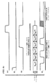
ここで図4a〜4eを参照して、通常動作モードとコマンド通信モードとに従う、メモリカード25におけるコントローラ30と結合したフラッシュメモリ装置10の動作を説明する。これらの動作モードは最新のフラッシュメモリ装置のための在来のフラッシュメモリインターフェイスプロトコルに実質的に対応し、従ってこれらの動作モードは本発明の好ましい実施形態に従うフラッシュメモリ装置10のための“レガシー”入出力プロトコルとして役立つと考えられる。
The operation of the
図4aは、コントローラ30からフラッシュメモリ装置10へのコマンドの伝達を示す。当該技術分野で知られているように、また以下でさらに詳述されるように、最新のフラッシュメモリ装置は、コントローラにより発せられてデータ入出力線を介して伝達される特定のコマンドに応答して動作する。この例では、コマンドCMDの伝達は、コントローラ30がコマンドラッチイネーブル信号CLEをハイアクティブ状態に、アドレスラッチイネーブル信号ALEを非アクティブロー状態に駆動して、アドレスではなくてコマンドが入出力線I/O1〜I/Onで伝達されることを示すことによって、行われる。チップイネーブル信号CE_がアクティブローにされて、在来の仕方でフラッシュメモリ装置10をイネーブルする。当該技術分野で知られているように、複数のフラッシュメモリ装置10がカード25内に設けられているならば、コントローラ30が通信のためにフラッシュメモリ装置10のうちの所望の1つを選択するときに個々のチップイネーブル信号CE_がコントローラ30により使用され得る。図4aに示されているコマンドCMDに対応する、コントローラ30により入出力線I/O1〜I/On上に与えられるデジタルワードは、コントローラ30が書き込みイネーブル線WE_でアクティブローパルスを発することによってストローブされ、線WE_上のパルスの立ち上がりエッジはI/O制御回路20にコマンドCMDを受け取らせて中にラッチ(latch in)させ、結局はコマンドレジスタ24(図2)に到達させる。コントローラ30は、その後、コマンドラッチイネーブル信号CLEを非アクティブロー状態に戻し、コマンド動作を終えることができる。もちろん、当該技術分野で知られているように、マルチワードコマンドまたは複数のシングルワードコマンドをこのようにして逐次伝達することができ、そのような伝達の間、コマンドラッチイネーブル線CLEはハイに保たれる。
FIG. 4 a shows the transmission of commands from the
図4aに示されている仕方で伝達される1つのコマンドは、メモリアドレスがコントローラ30によってフラッシュメモリ装置10へ伝達されることを示すコマンド(例えば、読み出し動作のためのコマンド00H、シリアルデータ入力プログラム、すなわち書き込み動作のためのコマンド10H)である。図4bは、本発明の好ましい実施形態に従う通常コマンド動作モードでの、フラッシュメモリ装置へのコントローラ30によるそのようなアドレスの伝達のタイミングを示す。図4bに示されている動作は、図4aのシーケンスに従うコマンド00Hの伝達に続き、次の信号シーケンスでのメモリアドレスの緊急送信を示す。
One command transmitted in the manner shown in FIG. 4a is a command indicating that the memory address is transmitted to the
この通常動作モードにおいて、割合に広い範囲のコマンドがコントローラ30によりフラッシュメモリ装置10へ伝達され得る。以下の表は、本発明のこの好ましい実施形態における代表的なコマンドセットをリストしている。

ここで図4bを参照して、本発明のこの好ましい実施形態に従うコントローラ30からフラッシュメモリ装置10へのメモリアドレスの送信を説明する。この動作において、コントローラ30はコマンドラッチイネーブル信号CLEを非アクティブローに駆動し、アドレスラッチイネーブル信号ALEをハイに駆動して、入出力線I/O1〜I/Onで(コマンド値ではなくて)アドレス値が伝達されることをフラッシュメモリ装置10に示す。チップイネーブル信号CE_もアクティブローに駆動されて、コントローラ30がこのアドレス情報の受信者としてフラッシュメモリ装置10を選択していることを示す。この動作において、コントローラ30は書き込みイネーブル信号WE_のアクティブローパルスを発し、その各パルスは、そのときにコントローラ30によりアドレス値の一部が入出力線I/O1〜I/Onで与えられることを示す。本発明のこの実施形態では、フラッシュメモリ10がこのエッジを使って入出力線I/O1〜I/Onのそのときの現在の状態を所望のメモリアドレスの一部としてアドレスレジスタ22(図2)の中にラッチできるように、このアドレス情報は書き込みイネーブル信号WE_の立ち上がりエッジ(すなわち、アクティブローパルスの末尾)と同期する。図4bの例で明らかであるように、メモリアドレスは複数ワードにわたって広がる(その幅は入出力線I/O1〜I/Onの数nにより決まる)。この場合、メモリアドレスは、書き込みイネーブル信号WE_の連続するアクティブローパルスと同期して与えられる4つのアドレスワードADD0〜ADD3を含む。
Referring now to FIG. 4b, the transmission of memory addresses from the
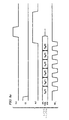
図4bに示されているアドレス値の伝達に続いて、コントローラ30はフラッシュメモリ装置10へのデータの書き込み、またはフラッシュメモリ装置10からのデータの読み出しを実行することができる。図4cは、本発明のこの好ましい実施形態に従って、通常動作モード(すなわち、“レガシー”モードで)書き込み動作を行うために伝達される信号を示す。図2のアーキテクチャに従って、このデータ書き込み動作は、データレジスタ14へのデータの書き込みである。本発明の好ましい実施形態に従って、データレジスタへの書き込みのコマンド(例えば、コマンド値80H)が、図4aに示されている仕方でもたらされ、それに続いてフラッシュメモリ装置10内の宛先メモリアドレスがコントローラ30によって伝達されるが、その両方が、図4cに関連して以下に記述される書き込み動作の前に行われる。データ書き込み動作を行うためにコントローラ30は、コマンドラッチイネーブル信号CLEとアドレスラッチイネーブル信号ALEとを両方とも非アクティブローに駆動して、フラッシュメモリ装置10に対して、書き込まれるべき入力データ(すなわち、コマンド値でもアドレス値でもない)が入出力線I/O1〜I/Onで伝達されることを示す。もちろん、この動作のためにチップイネーブル信号CE_もアクティブローに駆動される。コントローラ30は、その後、入出力線I/O1〜I/Onで与えられるデータの各バイトまたはワードとともに書き込みイネーブル信号WE_のアクティブローパルスを発する。本発明のこの実施形態では、コマンドおよびアドレス送信の場合と同じく、有効な入力データは書き込みイネーブル信号WE_の、各パルスの末尾の立ち上がりエッジと同期して与えられる。このエッジに応答して、フラッシュメモリ装置10は、入力データのワードまたはバイトに対応する入出力線I/O1〜I/Onのそのときの現在の状態をI/O制御回路20内のデータラッチの中に、または直接に(または事情次第で、結局は)バスDATA_BUSを介してデータレジスタ14にラッチする。図4cは、入出力線I/O1〜I/Onを介しての4つのワードDin(0)〜Din(3)の、書き込みイネーブル信号WE_の4つのパルスと同期しての伝達を示す。
Subsequent to the transmission of the address value shown in FIG. 4b, the
図4dは、本発明の好ましい実施形態に従う通常動作(“レガシー”)モードにおいて(フラッシュメモリ装置10からコントローラ30への)データ読み出し動作を実行するときのコントローラ30およびフラッシュメモリ装置10の動作を示す。データ書き込み動作の場合と同じく、この読み出し動作の前に(例えば、図4aに示されている)コマンドシーケンスおよび(例えば、図4bに示されている)アドレスシーケンスが前もって行われている。この読み出しの前に1つ以上の書き込み動作が前もって実行されているかも知れず(すなわち、この場合、その読み出しが、今書き込まれたばかりのと同じアドレスに対する読み出しであるならば、この読み出しは前の書き込みのベリファイとして役立つ)、あるいは(例えば、図4cに示されている)書き込み動作が、同じメモリアドレスへの読み出し−修正−書き込みシーケンスの形で、この読み出し動作後に実行され得る。読み出しの前のアドレスの伝達に応答して、そのアドレスに対応するメモリセルの内容が感知されてデータレジスタ14へ転送される。従って、図4dの読み出し動作は、データレジスタ14の現在のコメントの読み出しである。そして、この読み出し動作を行うために、コントローラ30は、図4aに関して前に記載された仕方でコマンド動作において適切なコマンド(例えば、コマンドE0h)を発する。
FIG. 4d illustrates the operation of
この動作において、書き込み動作のときと同じく、コントローラ30は、コマンドラッチイネーブル信号CLEとアドレスラッチイネーブル信号ALEとを両方とも非アクティブローに駆動し、チップイネーブル信号CE_をアクティブローに駆動している。コントローラ30は、書き込みイネーブル信号WE_を非アクティブハイにすることによって、所望の読み出し動作を示す。このデータ読み出し動作において、フラッシュメモリ装置10は、コントローラ30により生成された読み出しイネーブル信号RE_のアクティブローパルスの立ち下がりエッジに応答してデータワードDoutを出力する。従って、この通常動作モードにおいて、コントローラ30は、読み出しイネーブル信号RE_のアクティブローパルスを発し、その後に指定されたアクセス時間待つ(フラッシュメモリ装置10が、そのメモリセルの状態を感知する動作と、その感知した状態をそのデータレジスタ14へ転送し入出力線I/O1〜I/Onに出す動作とに関わる動作の一部または全部を行うことを可能にする)ことによって、フラッシュメモリ装置10からのデータの受け取りを同期化することができる。コントローラ30は、その後、フラッシュメモリ装置10からデータを受け取るために入出力線I/O1〜I/Onのデータ状態をその入力バッファの中にラッチすることができる。図4dの例では、4つのデータワードDout(0)〜Dout(3)が順に読み出され、チップイネーブル信号CE_の立ち上がりエッジがこの読み出し動作を終了させ、その後にフラッシュメモリ装置10は、I/O制御回路20内のその出力ドライバに入出力端子I/O1〜I/Onを高インピーダンス(“ハイ−Z”)状態に置かせる。
In this operation, as in the write operation, the
当該技術分野で知られているような、この通常動作(“レガシー”)モードに従う他の動作も好ましく利用可能である。例えば、コントローラ30は、図4aのタイミングの後に特定のステータスコマンド(例えば、コマンドコード70H)を発し、その読み出しイネーブル信号RE_のアクティブローパルスの発行に応答して入出力線I/O1〜I/Onを介してステータスレジスタ24の内容を受け取ることによって、この通常動作モードでステータスレジスタ24の内容を読み出すことができる。
Other operations following this normal operation ("legacy") mode, as known in the art, are also preferably available. For example, the
図4cおよび4dから明らかであるように、1つのデータワードまたはバイト(以降の記述では“データワード”と称される)が書き込みイネーブル信号WE_または読み出しイネーブル信号RE_の各サイクルの間にそれぞれ伝達される。そして、これらの図と前の説明とから明らかであるように、コントローラ30は、この通常動作モードにおいて書き込みイネーブル信号WE_と読み出しイネーブル信号RE_との両方を制御し、生じさせる。特に読み出し動作では、読み出しイネーブル信号RE_の各々の完全なサイクルの間に唯一のデータワードが読み出されるので、コントローラ30は、在来のフラッシュメモリタイミング要件および性能に従って、コントローラ自身がその読み出しデータストローブ(読み出しイネーブル信号WE_)を発し、また読み出されたデータを受け取ってラッチするのに充分な時間を有する。しかし、このレベルの性能は、フラッシュメモリカード25がコンピュータシステムで大容量記憶装置として使用されるときなど、フラッシュメモリ装置10の高速使用のためには必ずしも充分ではないかもしれない。さらに、この“レガシー”動作モードは、前述したUDMAインターフェイスプロトコルのもとなどでは、コントローラ30からホストシステムへの高速外部インターフェイスモードに追いついていけないかもしれない。
As is apparent from FIGS. 4c and 4d, one data word or byte (referred to as “data word” in the following description) is transmitted during each cycle of the write enable signal WE_ or the read enable signal RE_, respectively. The As is apparent from these figures and the previous description, the
従って、本発明の好ましい実施形態によれば、フラッシュメモリ装置10は、進歩した(アドバンスト)、より高い性能の、読み出しおよび書き込み動作モードを提供し、コントローラ30はそのアドバンストモードを利用するように構成される。このアドバンストモードを利用するときのフラッシュメモリ装置10およびコントローラ30の動作を、ここで、図5aおよび5bの流れ図および図6a〜6eのタイミング図と関連して詳しく説明する。
Thus, according to a preferred embodiment of the present invention, the
図5aおよび6a〜6cは、データ読み出し動作(すなわち、フラッシュメモリカード25における、フラッシュメモリ装置10からコントローラ30への)を行うときのフラッシュメモリ装置10の動作を示す。図5aのプロセス40で、フラッシュメモリ装置10とコントローラ30とはパワーアップされ、それはこれら両方の装置を、図4a〜4dに関して前に説明した通常動作モードにする(プロセス42)。プロセス44で、この通常モードでの読み出しおよび書き込み動作(そうであるならば)が、この通常動作(“レガシー”)モードで実行される。
FIGS. 5a and 6a-6c show the operation of the
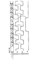
アドバンスト読み出し動作モードに入ることはプロセス46から始まり、ここでコントローラ30は、図4bに関して前に説明したように、通常動作モードに従ってメモリアドレス値をフラッシュメモリ装置10に対して発する。プロセス46でコントローラ30により発せられるメモリアドレスは、このアドバンスト動作モードでデータがそこから読み出されるところの初めのメモリアドレスであって、好ましくは前述した対応する読み出しアドレス入力コマンドの送信に続く。プロセス48で、コントローラ30は、フラッシュメモリ装置10に対して“データ転送開始(initiate data transfer)”、あるいは“IDT”、コマンドシーケンスを発する。図6aは、この動作をさらに詳しく示す。
Entering the advanced read mode of operation begins at
本発明の好ましい実施形態に従って、“IDT”コマンドは、プロセス48でアドバンストデータ転送モードを開始させるためにコントローラ30によってフラッシュメモリ装置に対して発せられる。このコマンドは図4aに関して前に説明したコマンドの発行と同様にして発せられ、コントローラ30がチップイネーブル信号CE_をアクティブローに、アドレスラッチイネーブル信号ALEを非アクティブローに、コマンドラッチイネーブル信号CLEをアクティブハイに、それぞれ、駆動する。書き込みイネーブル信号WE_のアクティブローパルスの立ち上がりエッジは、コントローラ30によって入出力線I/O1〜I/On上へ駆動されたIDTコマンド値IDT_CMD(これは他の割り当てられたコマンド値とは異なる値を有するバイナリワードである)のためのデータストローブとして役立つ。書き込みイネーブル信号WE_がハイにされてから所定時間後に、コントローラ30は入出力線I/O1〜I/Onを高インピーダンス状態にする。そして、書き込みイネーブル信号WE_の立ち上がりエッジ(そのときIDTコマンドを中にストローブする)からのもう1つの経過時間trel の後、コントローラ30はその読み出しイネーブル信号RE_の制御を放棄して、フラッシュメモリ装置10の制御ロジック18が対応する線RE_の状態を駆動することを可能にする(コントローラ30とのデータ競合を敢行せずに)。
In accordance with the preferred embodiment of the present invention, an “IDT” command is issued by the
IDTコマンドがフラッシュメモリ装置10の中にラッチされてこの装置により実行されると、フラッシュメモリ装置10は高速モード読み出しデータ転送プロセス50を開始する。図6aに示されているように、この読み出しデータ転送プロセスは、書き込みイネーブル信号WE_の立ち上がりエッジの後、ゼロではないアクセス時間が経過した後に、フラッシュメモリ装置10が第1の有効出力データワードDout (0)を発することから始まる。この第1の出力データワードDout (0)を与えた後、フラッシュメモリ装置10は、追加の出力データワードDout (1)以下参照と同期して、読み出しイネーブル信号RE_のアクティブパルスを発し始める。本発明のこの好ましい実施形態に従って、フラッシュメモリ装置10自体により駆動される読み出しイネーブル信号RE_の各エッジ(立ち下がりおよび立ち上がり)と同期して1つのデータワードDout (k)が発せられる。図6aの例では、各出力データワードDout (k)はそのストローブエッジに1つのゼロではないアクセス時間だけ遅れて続くが、その代わりに各読み出しイネーブル信号RE_エッジはそれに対応する有効データワードDout(k)の中でコントローラ30に対して発せられ(あるいは発せられるべく遅延され)てもよい。
When the IDT command is latched into and executed by the
従って、本発明の好ましい実施形態に従って、フラッシュメモリ装置10がこのアドバンストモードで入出力線I/O1〜I/Onを介してデータをコントローラ30に与える速度は、通常動作モード(図4d)におけるデータ速度より大幅に速く、代表的な実施例ではこのデータ速度の2倍に近い。このより高いデータ速度は、或る程度、フラッシュメモリ装置10が読み出しイネーブル信号RE_の読み出しデータストローブエッジを発することを許すことによって可能にされ、コントローラ30がこれらの読み出しデータストローブエッジを発するとすれば、伴うことになる伝播遅延および所要のタイミングウィンドウをなくす。
Therefore, according to a preferred embodiment of the present invention, the speed at which the
しかし、当業者にとっては明らかであるように、出力データが入出力線I/O1〜I/Onで与えられる増大した速度は、他の全ての要素が同等であるならば、この読み出し動作において主としてフラッシュメモリ装置10のI/O制御回路20内の出力駆動回路から、フラッシュメモリカード25内での消費電力を大幅に増大させる。この電力消費は、最新の傾向がそうであるように、データワード幅(すなわち、入出力線I/O1〜I/Onの数n)が大きくなるに連れて、悪化する。本発明の好ましい実施形態に従って、以下に説明するように、この電力消費は入出力線I/O1〜I/Onにおける出力信号の電圧振幅を減少させることによって大幅に低減される。
However, as will be apparent to those skilled in the art, the increased speed at which the output data is provided on input / output lines I / O1-I / On is mainly in this read operation if all other factors are equal. The power consumption in the
在来のフラッシュメモリ装置は周知の3.3ボルトのバス標準規格を利用し、この規格では最低ハイレベル出力電圧VOHは2.4ボルトであり、最高のローレベル出力電圧VOLは0.4ボルトであり、公称電圧振幅は約3.3ボルトである。この標準規格によれば、当該技術分野で周知されているように、これらの電圧は名目上3.30ボルトの電源電圧に基づき、それは2.70ボルトおよび3.60ボルトの間の仕様範囲を有する。最新のフラッシュメモリ装置のための通常動作モードでは、出力データ速度は25MHz(すなわち、40ナノ秒毎のデータ遷移)であり、所与の入出力線I/Okが各サイクルでデータ遷移を行うという最悪の場合には、フラッシュメモリ装置10は入出力線I/Okの静電容量を12.5MHzの周波数で充電するように要求される。この入出力線I/Okについて65pFの代表的な線の静電容量を仮定すれば、1つの入出力線I/Okについて、ミリアンペアを単位として表した電流消費は、
Ik =f*C(VOH−VOL)
から計算することができ、この例では、ハイデータレベルとローデータレベルとの間の代表的な3.3ボルトの振幅を用いれば、
Ik =12.5*0.065(3.3)=2.681mA
という結果となる。読み出しイネーブル信号RE_を駆動するときに消費される電流は、その対応する導体を各遷移のために充電しなければならないので、電流Ik のものの2倍となる。従って、この例について在来の通常動作モードで消費される総電流は、8本の入出力線I/O1〜I/O8を仮定すれば、
Itotal =8(2.681)+2(2.681)=26.81mA
となる。
Conventional flash memory devices utilize the well-known 3.3 volt bus standard, where the lowest high level output voltage V OH is 2.4 volts and the highest low level output voltage V OL is 0. 4 volts, and the nominal voltage amplitude is about 3.3 volts. According to this standard, as is well known in the art, these voltages are nominally based on a power supply voltage of 3.30 volts, which has a specification range between 2.70 volts and 3.60 volts. Have. In normal operation mode for modern flash memory devices, the output data rate is 25 MHz (ie, data transitions every 40 nanoseconds) and a given input / output line I / Ok performs data transitions in each cycle. In the worst case, the
I k = f * C (V OH −V OL )
In this example, using a typical 3.3 volt amplitude between the high and low data levels,
I k = 12.5 * 0.065 (3.3) = 2.681 mA
As a result. The current consumed when driving the read enable signal RE_ is twice that of the current I k since its corresponding conductor must be charged for each transition. Therefore, assuming that eight input / output lines I / O1 to I / O8 are assumed as the total current consumed in the conventional normal operation mode for this example,
I total = 8 (2.681) +2 (2.681) = 26.81 mA
It becomes.
本発明の好ましい実施形態によれば、バス電圧は、この在来の3.3vバスレベルから例えば、約1.80ボルトの公称電圧振幅を定める約1.8ボルトのバス電圧へ、大幅に低減される。この場合、最低ハイ出力レベル電圧VOH-Rの限界例は約1.44ボルト(公称電源電圧の80%)であり得、最高ロー出力レベル電圧VOL-Rの例は約0.36ボルト(公称電源電圧の20%)であり得る。この低減電圧動作では、これらの電圧は名目上1.80ボルトである電源電圧に基づき、約1.60ボルト〜約2.0ボルトまで変動することを許される。最善の場合(データ転送に関して。電流消費に関しては最悪の場合)の50MHzのデータ速度を仮定すると、入出力線I/O1〜I/Onのための充電周波数は25MHzとなる。単一の入出力線I/Okについて消費される電流Ikは、ハイデータレベルとローデータレベルとの間の代表的な1.8ボルトの振幅を用いて、
Ik =25*0.065(1.8)=2.925mA
と計算され得る。このように、この入出力線あたりの電流消費は、アドバンスト動作モードについて余り違わないが、2倍のデータ速度を提供する。しかし、読み出しイネーブル信号RE_は通常動作モードの場合と同じ周波数で動作する(しかし、立ち上がりエッジだけではなくて各エッジで1データワードをクロックする)。しかし、その電圧振幅も、1.8ボルトバス電圧で動作するので、低減され、従って、その電流消費は入出力線のうちの1つについてのものと同じである。従って、この例についてアドバンスト動作モードで消費される総電流は、再び8本の入出力線I/O1〜I/O8を仮定すれば、
Itotal =8(2.925)+1(2.925)=26.33mA
となり、これは3.3ボルトバス電圧で動作する在来のフラッシュメモリカードについてのものより僅かに少ない。また、この僅かに少ない電流消費は入出力信号のためのより低い電圧振幅(3.3ボルトに対して1.8ボルト)で達成されるので、このアドバンスト動作モードで消費される電力は、在来のフラッシュメモリカードで消費されるものよりも大幅に少ない。これらの例では、在来の8I/Oフラッシュメモリにおいて通常動作モードで消費される電力は約88mW(3.3ボルト×26.81mA)であり、前述した本発明の好ましい実施形態の例により消費される電力は約47mW(1.8ボルト×26.33mA)である。電力消費のこの大幅な低減は、大きなバーストについてのデータ速度の2倍に近い、データ転送速度の大幅な改善と結合して達成される。
In accordance with a preferred embodiment of the present invention, the bus voltage is significantly reduced from this conventional 3.3v bus level, for example, to a bus voltage of about 1.8 volts defining a nominal voltage amplitude of about 1.80 volts. Is done. In this case, the limit of the lowest high output level voltage V OH-R may be about 1.44 volts (80% of the nominal power supply voltage), and the example of the highest low output level voltage V OL-R is about 0.36 volts. (20% of the nominal power supply voltage). In this reduced voltage operation, these voltages are allowed to vary from about 1.60 volts to about 2.0 volts based on a power supply voltage that is nominally 1.80 volts. Assuming a data rate of 50 MHz in the best case (for data transfer, worst case for current consumption), the charging frequency for the I / O lines I / O1-I / On is 25 MHz. The current I k consumed for a single input / output line I / Ok is typically 1.8 volt amplitude between the high and low data levels,
I k = 25 * 0.065 (1.8) = 2.925 mA
And can be calculated. Thus, this current consumption per input / output line is not much different for the advanced mode of operation, but provides twice the data rate. However, the read enable signal RE_ operates at the same frequency as in the normal operation mode (but clocks one data word at each edge, not just the rising edge). However, its voltage amplitude is also reduced because it operates at a 1.8 volt bus voltage, so its current consumption is the same as for one of the input / output lines. Therefore, the total current consumed in the advanced operation mode for this example is again assumed to be 8 input / output lines I / O1 to I / O8.
I total = 8 (2.925) +1 (2.925) = 26.33 mA
Which is slightly less than for conventional flash memory cards operating at 3.3 volt bus voltage. Also, since this slightly less current consumption is achieved with a lower voltage swing for input and output signals (1.8 volts versus 3.3 volts), the power consumed in this advanced mode of operation is not present. Significantly less than what would be consumed by future flash memory cards. In these examples, the power consumed in the normal operation mode in a conventional 8I / O flash memory is about 88 mW (3.3 volts × 26.81 mA), which is consumed by the above-described preferred embodiment example of the present invention. The power applied is about 47 mW (1.8 volts x 26.33 mA). This significant reduction in power consumption is achieved in combination with a significant improvement in data transfer rate, which is close to twice the data rate for large bursts.
従って、アドバンスト読み出しデータ転送が(在来のフラッシュメモリ装置と関連して)これらのより低いバス電圧で実行される本発明の好ましい実施形態によれば、アドバンストモードで消費される電流は通常動作モードの在来のフラッシュメモリ装置により消費されるものより決して悪くない。また、フラッシュメモリ装置10が通常動作モードで動作する能力も有する本発明のこの好ましい実施形態によれば、より低いバス電圧はアドバンストモードおよび通常動作モードの両方にも、またコマンドおよびアドレス値の伝達を含む他の動作のためにも、使用される。このように、フラッシュメモリ装置10は、データ転送時に、在来のフラッシュメモリ装置より少ない電力を消費する。
Thus, according to a preferred embodiment of the present invention in which advanced read data transfer is performed at these lower bus voltages (in conjunction with conventional flash memory devices), the current consumed in advanced mode is normal operation mode. No worse than that consumed by conventional flash memory devices. Also, according to this preferred embodiment of the present invention, where the
前述したものから明らかなように、コマンド信号およびアドレス信号は通常動作モードで伝達される。実現を容易にするために、これらの信号の伝達のためのバス電圧もより低いバス電圧(例えば、1.8ボルト)に好ましく保たれ、フラッシュメモリカード25の電力消費の付加的な低減を提供する。
As apparent from the foregoing, the command signal and the address signal are transmitted in the normal operation mode. For ease of implementation, the bus voltage for transmission of these signals is also preferably kept at a lower bus voltage (eg, 1.8 volts), providing an additional reduction in power consumption of the
図5aに戻って参照すると、本発明のこの実施形態に従うフラッシュメモリ装置10は、コントローラ30からの中断リクエストに応答することができる。本発明によれば、例えばその内部受信データバッファが満杯であるなどの、いくつかの理由のうちのいずれか1つのために読み出しデータ転送の中断がコントローラ30により必要と見なされ得ると考えられる。従って、図5aの判定51は、そのような中断が必要とされるか否かを判定する。必要でなければ、図6aに関して前に説明したように高速読み出しデータ転送がプロセス56で続行される。
Referring back to FIG. 5 a, the
コントローラ30が読み出しデータ転送の中断を要求すれば(判定51が肯定であれば)、それはプロセス52で中断リクエストを発する。この代表的な実施例では、このリクエストは、コントローラ30が読み出し転送動作中にアドレスラッチイネーブル信号ALEでアクティブハイレベルをアサートすることによってなされる。図6bは、アドバンストモードでの読み出しデータ転送中に(すなわち、このモードが起動されてデータ転送が始まった後に)発生した、そのような中断動作を示す。図6bの例では、コントローラ30は、フラッシュメモリ装置10からコントローラ30へのデータ転送中にアドレスラッチイネーブル信号ALEをアサートすることによってデータ転送中断をリクエストする。応答して、フラッシュメモリ装置10は(示されているようにローレベルのときまたはハイレベルのときに)読み出しイネーブル信号RE_を中断させ、従って、読み出しイネーブル信号RE_が中断させられた後の次のデータワードの発行を遅延させる。このアドバンストモードで読み出しイネーブル信号RE_と入出力線I/O1〜I/Onとの速いスイッチング速度が与えられたとすれば、中断をリクエストするためにアドレスラッチイネーブル信号ALEがアクティブハイに駆動された後に1つまたは2つの付加的なデータワードと読み出しイネーブル信号RE_の対応するエッジとがフラッシュメモリ装置10によって駆動され得ると考えられる。この例では、コントローラ30は出力データワードDout (4)の間にアドレスラッチイネーブル信号ALEをアサートし、フラッシュメモリ装置10は、出力データワードDout (6)の間、読み出しイネーブル信号RE_と入出力線I/O1〜I/Onとのさらなる遷移を抑えることによって、応答する。
If the
さらなるデータ転送のこの中断は、アドレスラッチイネーブル信号ALEを非アクティブ化し、これにより中断を終了させるためにコントローラ30がプロセス54を実行するまで続く。図6bに示されているように、中断状態は、コントローラ30がアドレスラッチイネーブル信号ALEを非アクティブロー状態にしたときに、終了させられる。本発明のこの実施形態によれば、アドレスラッチイネーブル信号ALEのこの遷移は、フラッシュメモリ装置10からの次の出力データワード、すなわちこの例ではデータワードDout (7)のための読み出しデータストローブとして役立つ。この最初の中断後データワードの後に、フラッシュメモリ装置10は、示されているように読み出しイネーブル信号RE_の遷移をアサートすることによって読み出しストローブ信号を再び生成する。この例において、読み出しイネーブル信号RE_の次の遷移は、中断期間終了後の第2の出力データワードDout (8)のためのストローブである。図6bに示されているように、アドバンストモード読み出しデータ転送はプロセス56で続行する。
This interruption of further data transfer continues until the
図5aに戻って参照すると、アドバンストモード読み出しデータ転送は、コントローラ30がこの転送を終了させることを望むようなときまで続行し、これをプロセス58,59でフラッシュメモリ装置10に対して示す。通常、この転送は、フラッシュメモリ装置10内の1つのページの末尾に到達しているとコントローラ30が判定したときに終了させられるが、この転送は他の理由(例えば、この動作のための所望のデータの全体を受け取ったとき)からもコントローラ30により終了させられ得る。
Referring back to FIG. 5a, the advanced mode read data transfer continues until such time as the
この例に従って、このデータ転送を終了させるために、コントローラ30は、始めに、例えば前述したようにアドレスラッチイネーブル信号ALEのアクティブハイレベルをアサートすることによって、プロセス58で中断を発する。図6cは終了プロセス58,59のこの例を示し、そこにはアドバンスト読み出しデータ転送動作中のアドレスラッチイネーブル信号ALEの遷移が示されている。プロセス58のこの中断動作は、コントローラ30がこの中断動作中にプロセス59を実行することによってアドバンスト読み出しデータ転送の終了に変換される。代わりに、プロセス59を、フラッシュメモリ装置10自体がその出力データがページの末尾に達したと判定した後に実行することができ、その場合にはフラッシュメモリ装置10自体は読み出しイネーブル信号RE_をその最後のレベルに保つとともに入出力線I/O1〜I/On上の現在の(すなわち、最後の)出力データワードを維持し、この場合、アドレスラッチイネーブル信号ALEは非アクティブローに留まる。図6cに示されている例では、このデータ転送は、アドレスラッチイネーブル信号ALEがアクティブハイである間にコントローラ30がコマンドラッチイネーブル信号CLEでアクティブハイレベルをアサートすることによって終了させられる。コマンドラッチイネーブル信号CLEのこの遷移に応答して、フラッシュメモリ装置10は、その出力ドライバを制御して入出力線I/O1〜I/Onを高インピーダンス状態にし、また読み出しイネーブル信号RE_に対応する導体のこのフラッシュメモリ装置による制御を放棄し、その両方の場合にコントローラ30がデータ競合問題を避けながら適時にこれらの線の制御を取ることを許す。図6cの例において示されているように、中断動作と終了動作とは読み出しイネーブル信号RE_がローレベルであるときに発生したので、コントローラ30は、読み出しイネーブル信号RE_の制御を取ると、対応する線上に非アクティブハイレベルを駆動し、図に示すように遷移を生じさせる。中断動作および終了動作が読み出しイネーブル信号RE_が既にハイレベルであるときに発生したならば、もちろん、この線上にはなんらの遷移も生じない。
In accordance with this example, to complete this data transfer,
フラッシュメモリ装置10はその後、通常動作モード(“レガシー”モード)に戻り、制御を図5aの流れ図のプロセス44に返す。本発明のこの好ましい実施形態では、新しいアドバンストモード読み出しデータ転送は開始プロセス48の他の1つの事例を必要とする。
The
さらに代案では、コントローラ30がチップイネーブル信号CE_をアサート解除すれば、無条件終了が発生する。しかし、この制御されない終了は“グリッチ”と、フラッシュメモリ装置10およびコントローラ30の内部および外部の両方における他のスプリアス不定事象をもたらす可能性があると考えられる。
Further alternatively, if the
本発明のこの好ましい実施形態に従って、コントローラ30からフラッシュメモリ装置10へのデータ転送のためにも、換言すれば書き込みデータ転送動作のためにも、アドバンスト高性能モードが提供される。以下に説明するように、図5bの流れ図と、図6aおよび6d〜6eのタイミング図とが、この動作を示す。
In accordance with this preferred embodiment of the present invention, an advanced high performance mode is provided for data transfer from the
アドバンストモード書き込みデータ転送を行うために、フラッシュメモリ装置10は、プロセス60で入る通常動作モードから始める。読み出しデータ転送の場合と同様に、通常モード動作(あるならば)が始めにプロセス62で実行され得る。プロセス64で、コントローラ30は、図4bに関して前に説明したようにこの通常動作モードでアドレス値をフラッシュメモリ装置10に対して発する。そして、プロセス66で、コントローラ66は、図6aに関して前に説明したアドバンスト読み出しデータ転送のために行われるのと同様の仕方でアドバンストデータ転送モードを開始する。このアドバンストモードでの書き込みデータ転送は、プロセス66を通して、読み出しデータ転送が行われたのと実質的に同一の仕方で実行されると考えられる。従って、例えば、プロセス66で発せられるコマンド値IDT_CMDは読み出しおよび書き込みデータ転送動作の両方のために同じであると考えられる。あるいは、これら2つの動作のために互いに別々のコマンド値が割り当てられてもよい。
To perform the advanced mode write data transfer, the
プロセス68で、コントローラ30およびフラッシュメモリ装置10はアドバンスト書き込みデータ転送を実行する。図6dは、コマンド値IDT_CMDと、コマンドラッチイネーブルCLEのアクティブハイレベルと、書き込みイネーブル信号WE_のアクティブローパルスとの組み合わせがコントローラ30によりフラッシュメモリ装置10へ発せられてアドバンストモードデータ転送を開始するプロセス66を含む、この動作の例における信号のタイミングを示す。前の例の場合と同様に、アドレスラッチイネーブル信号ALEは非アクティブローレベルに保たれ、チップイネーブル信号CE_はアクティブローに保たれる。そして、この動作はデータ書き込みであるので、読み出しイネーブル信号RE_(図6dには示されていない)はコントローラ30により終始非アクティブハイに保たれる。書き込みデータ転送プロセス68はコントローラ30の完全制御下に留まるので、本発明のこの実施形態では、コマンドIDT_CMDの発行と書き込みデータ転送の開始との間の待ち時間は、読み出しデータ転送(図6a)における第1の出力データワードの前のものより遥かに短くなり得る。好ましくは、図に示されているように、開始コマンドIDT_CMDに対応する書き込みイネーブル信号WE_のパルスの立ち上がりエッジと、第1の入力データワードDin(0)に対応する書き込みイネーブル信号WE_の第1のパルスの立ち下がりエッジとの間に所定時間が経過する。
In
いったん書き込みデータ転送が始まれば、本発明のこの好ましい実施形態において、書き込みイネーブル信号WE_の立ち下がりエッジおよび立ち上がりエッジの両方が、コントローラ30によりアサートされる書き込みデータストローブとして作用する。図6dに示されているように、これは、コントローラ30が書き込みイネーブル信号WE_の各エッジと同期して新しい有効な書き込みデータワードDin(k)を入出力線I/O1〜I/On上に発することを可能にする。その結果として、このアドバンストモードにおける書き込みデータ転送速度は、同じ書き込みイネーブル信号WE_周波数について、通常動作モード書き込み動作のデータ速度の2倍近くになり得る。
Once the write data transfer begins, in this preferred embodiment of the present invention, both falling and rising edges of the write enable signal WE_ act as write data strobes asserted by the
本発明のこの実施形態によれば、図5bに戻って参照すると、アドバンストモード書き込みデータ転送中に中断判定69も実行される。通常、書き込み中断の必要性はコントローラ30によってのみ決定され、フラッシュメモリ装置10がこのデータ速度でバッファオーバーフローなどなしに入力データを受信できると考えられる。中断が不要ならば(判定69は否定)、プロセス72でデータ転送が続行される。コントローラ30がそれを必要とするならば(判定69が肯定)、プロセス70で書き込みデータ転送の中断が行われる。この例では、中断プロセス70は、単にコントローラ30が書き込みイネーブル信号WE_の状態を必要なだけ延長することによって行われる。この中断はいずれの状態でも(書き込みイネーブル信号WE_がハイに保たれた状態でも、あるいはローに保たれた状態でも)実行され得る。図6dは書き込みデータワードDin(2)の持続時間中の中断プロセス70を示し、このとき書き込みイネーブル信号WE_はローに保たれる。もちろん、コントローラ30は中断プロセス70中は付加的な書き込みデータワードDin(k)を発しない。中断期間の終止は、書き込みデータ転送を続行するために(プロセス72)コントローラ30が単に書き込みイネーブル信号WE_の遷移を、図6dに示されている例では次の有効な書き込みデータワードDin(3)とともに、駆動することによって行われる。
According to this embodiment of the present invention, referring back to FIG. 5b, a
そして、読み出しデータ転送の場合と同じく、データおよび制御信号(入出力線I/O1〜I/Onと、書き込みイネーブル信号WE_のための線)の電圧レベルは、例えばハイロジックレベルとローロジックレベルとの間の1.8ボルトの“振幅”を伴って、好ましくは在来のレベルよりは低い電圧レベルである。前に詳述したように、この低電圧バスは、このアドバンスト書き込みデータ転送モードにより消費される電力を、半分のデータ速度で通常動作モードで動作している在来のフラッシュメモリシステムにおいて消費されるものと同じまたはそれより低く保つ。 As in the case of read data transfer, the voltage levels of data and control signals (input / output lines I / O1 to I / On and lines for the write enable signal WE_) are, for example, a high logic level and a low logic level. Preferably, the voltage level is lower than the conventional level, with an “amplitude” of 1.8 volts between. As detailed above, this low voltage bus consumes the power consumed by this advanced write data transfer mode in a conventional flash memory system operating in normal operation mode at half the data rate. Keep the same or lower than the one.
図5bに戻って図6eと組み合わせて参照すると、書き込みデータ転送の終了は、読み出しデータ転送の終了と同じ仕方で行われる。コントローラ30は、転送を中断させるためにアドレスラッチイネーブル信号ALEをプロセス74でアクティブハイレベルにアサートし、その後に(アドレスラッチイネーブル信号ALEをハイに保ちながら)プロセス76でコマンドラッチイネーブル信号CLEをアクティブハイレベルにアサートし、これがそのとき書き込みデータ転送を終了させる。図6eは、書き込みデータ転送を終了させるときの種々の信号のタイミングを示す。書き込みイネーブル信号WE_は、図6eに示されているようにハイレベルに保たれるか、あるいは(この例では)最後のデータワードDin(5)がラッチされた後にローレベルからハイレベルにされる。アドレスラッチイネーブル信号ALEおよびコマンドラッチイネーブル信号CLEのハイレベルを所定のパルス幅にわたって保つことによって行われるアドバンストモード書き込みデータ転送の終了の後、フラッシュメモリ装置10およびコントローラ30の通常動作モードに再び入る。
Referring back to FIG. 5b and in combination with FIG. 6e, the end of the write data transfer is performed in the same manner as the end of the read data transfer. The
この例では、アドバンストモードを起動するためにはコマンドの実行が必要とされることを考慮すると、また、データ転送の終了時に(すなわち、コマンドの実行を必要とせずに)フラッシュメモリ装置10の動作が通常動作モードに戻ることを考慮すると、通常動作モードは実際上“デフォルト”動作モードである。その代わりに、フラッシュメモリ装置10がいったんアドバンストデータ転送モードになったならば、通常動作モードに戻るコマンドがコントローラ30により発せられてフラッシュメモリ装置10により実行されるまでフラッシュメモリ装置10がそのモードに留まるように、アドバンストデータ転送モードおよび通常動作モードの両方に入るためにコマンドの実行が必要とされるようにフラッシュメモリ装置10が構成されてもよい。もちろん、このようなアプローチは、コマンドシーケンスの性質において付加的なオーバーヘッドを必要とする。
In this example, considering that a command must be executed to activate the advanced mode, and the operation of the
さらに、その代わりに、フラッシュメモリ装置10を通常動作モードにするためにコマンドがコントローラ30により発せられるまで全てのデータ転送がアドバンストモードで行われるように、フラッシュメモリ装置10の“デフォルト”動作モードがアドバンストデータ転送モードであり得るということが考えられる。本発明のこの代わりの実施形態では、フラッシュメモリ装置10がいったん通常動作モードになったならば、データ転送の完了は、フラッシュメモリ装置10がアドバンストデータ転送モードに戻るという結果をもたらす。
Further, instead, the “default” operating mode of the
図7は、本発明のこの代わりの好ましい実施形態に従うフラッシュメモリ装置10の動作を示し、アドバンストデータ転送モードは実際上“デフォルト”モードである。プロセス80で、フラッシュメモリ装置10とコントローラ30とはパワーアップされるか、さもなければリセット動作を終え、コマンドの発行あるいは実行を必要とすることなくプロセス82で実際上デフォルト状態としてのアドバンスト動作モードに入る。プロセス84で、実際上図6b〜6dに関して前に説明したように、読み出しおよび書き込み動作がアドバンストデータ転送動作モードで実行される。このアドバンストモードでは、例えば図6cに関して前に説明したように中断動作などが実行され得ると考えられ、さらに、アドレス、コマンド、およびステータス伝達動作のような他の動作が、所望ならば、なお通常動作モードのアプローチに従い得ると考えられる。
FIG. 7 illustrates the operation of the
プロセス86で、本発明のこの好ましい実施形態に従うフラッシュメモリカード25は、コントローラ30が1つのアドレス値をフラッシュメモリ装置10に対して発して通常動作モード転送が始まるべきメモリ位置を示すことによって、通常のデータ転送、あるいは“レガシー”データ転送に備える。プロセス88で、コントローラ30は通常動作モードを開始させるコマンドシーケンスを発する。このコマンドシーケンスは図6aに関して前に説明したものに実質的に対応し、このコマンドシーケンス自体は通常動作モードに従って好ましく動作すると考えられる(コマンドコード値は単一バイト値であると考えられる)。コマンド88に応答して、フラッシュメモリ装置10は、データ転送の方向に応じて、例えば図4cおよび4dに関して前に説明したように、通常動作モード読み出しまたは書き込みデータ転送動作を実行する。本発明のこの実施形態では、コントローラ30は、前述したように、読み出しデータストローブおよび書き込みデータストローブクロック信号の両方を好ましく発する。
In
そして、本発明のこの代わりの好ましい実施形態によれば、データ転送終了時に通常動作モードから出る。図7の例では、図5aおよび5bに関しての前に説明した場合と同様に、プロセス92でコントローラ30が中断信号(例えば、アドレスラッチイネーブル信号のアクティブレベル)を発したことによるデータ転送の終了後、コントローラ30はプロセス93で(例えば、コマンドラッチイネーブル信号のアクティブレベルを発することにより)転送を終了させる。本発明のこの好ましい実施形態による通常動作モードのデータ転送の終了のときに、制御をプロセス84に戻し、ここでアドバンストデータ転送モードに再び入って、プロセス84で希望通りに読み出しおよび書き込みデータ転送動作が実行される。
And according to this alternative preferred embodiment of the invention, the normal operation mode is exited at the end of the data transfer. In the example of FIG. 7, after the completion of the data transfer due to the
本発明のこの代わりの好ましい実施形態を超える、フラッシュメモリ装置10の種々の動作モードに入り、また出ることについての他の代わりのアプローチは本願明細書を参照した当業者にとっては明らかであると考えられ、また、これらの実施例および他のそのような代わりの実施例も特許請求の範囲に記載された本発明の範囲内にあると考えられる。
Other alternative approaches to entering and exiting the various modes of operation of
ここで図8a〜8eを参照して、本発明の第2の好ましい実施形態に従う、フラッシュメモリカード25の文脈におけるフラッシュメモリ装置10とコントローラ30との間の信号のタイミングを以下に詳しく説明する。本発明のこの第2の好ましい実施形態に従うアドバンストモードに入り、出るプロセス全体と、このモード中の動作とは、読み出し動作について図5aに関して、また書き込み動作について図5bに関して前に説明したプロセスに好ましくは従う。従って、これらのプロセスについての詳しい説明を図8a〜8eと関連して繰り返されない。
8a-8e, the timing of signals between the
本発明の第1の好ましい実施形態に関して前に説明したように、フラッシュメモリ装置10およびコントローラ30は、パワーアップ後、通常動作(“レガシー”)モードになる。従って、この通常モードでの読み出しおよび書き込み動作(あるならば)は、ユーザの希望通りに行われる。そのとき、読み出し動作のためのアドバンスト動作モードに入る動作は、このアドバンスト動作モードでデータが読み出されることになる最初のメモリアドレスに対応するメモリアドレス値をコントローラ30が通常動作モードにおいてフラッシュメモリ装置10に対して発することによって行われる。前の場合と同じく、このメモリアドレスは、アドレスラッチイネーブル信号ALEのアクティブレベルと組み合わされて入出力線I/O1〜I/On上に置かれる。
As previously described with respect to the first preferred embodiment of the present invention,
このメモリアドレスが伝達された後、コントローラ30は、チップイネーブル信号CE_アクティブロー、アドレスラッチイネーブル信号ALE非アクティブロー、およびコマンドラッチイネーブル信号CLEアクティブハイによって、前の場合と同様に“データ転送開始”、すなわち“IDT”、コマンドシーケンスをフラッシュメモリ装置10に対して発する。図8aはこの動作を示す。書き込みイネーブル信号WE_のアクティブローパルスの立ち上がりエッジは、コントローラ30によって入出力線I/O1〜I/On上に駆動されたIDTコマンド値IDT_CMD(他の割り当てられたコマンド値とは異なる値を有するバイナリワードである)のためのデータストローブとして作用する。書き込みイネーブル信号WE_がハイにされてから所定時間後に、コントローラ30は入出力線I/O1〜I/Onを高インピーダンス状態にする。
After the memory address is transmitted, the
本発明のこの第2の好ましい実施形態に従って、フラッシュメモリ装置10は、読み出しイネーブルストローブ信号RE_の制御を取ってこれを駆動する。従って、図8aに示されているように、IDTコマンドをストローブする書き込みイネーブル信号WE_の立ち上がりエッジから時間trel が経過したとき、コントローラ30はその読み出しイネーブル信号RE_の制御を放棄する。フラッシュメモリ装置10の制御ロジック18は、その後、コントローラ30と競合せずに対応する線RE_の状態を駆動することができる。フラッシュメモリ装置10は、その後、高速アドバンストモード読み出しデータ転送を実行し始める。本発明のこの第2の好ましい実施形態に従って、図8aに示されているように、フラッシュメモリ装置10は、レガシーモードで利用可能なものより高い周波数の読み出しイネーブル信号RE_と結合した、レガシーモードのものより高いデータ速度で、アドレス指定されたメモリセルからのデータを与える。
In accordance with this second preferred embodiment of the present invention, the
例えば、フラッシュメモリ装置10は、このアドバンストモードにおいて、レガシーモードにおけるこの信号の周波数の2倍の周波数でのこの装置による読み出しイネーブル信号RE_の駆動と結合した、レガシーモードでデータが与えられる周波数の2倍の周波数で、出力データを入出力線I/Oで与えることができる。レガシーモードでの最高の利用可能なデータ転送速度および読み出しストローブ周波数が25MHzである例について、アドバンストモードデータ転送速度および読み出しイネーブル信号RE_の周波数は50MHzの高さであり得る。フラッシュメモリ装置10自体が読み出しイネーブル信号RE_およびデータワードの発信源であるので、これらの信号がフラッシュメモリ装置10により作られる周波数はコントローラ30の直接制御下にはない。
For example, in this advanced mode, the
図8aは、このアドバンストモード読み出し動作を示す。読み出しデータ転送プロセスは、書き込みイネーブル信号WE_の立ち上がりエッジからゼロではないアクセス時間が経過した後に、フラッシュメモリ装置10が第1の有効出力データワードDout (0)を発することから始まる。第1の出力データワードDout (0)後に、フラッシュメモリ装置10は、付加的な出力データワードDout (1)以下参照と同期して読み出しイネーブル信号RE_のアクティブパルスを発し始める。本発明のこの好ましい実施形態によれば、読み出しイネーブル信号RE_の各々の完全なサイクルと同期して1つのデータワードDout (k)が発せられる。図8aの例では、読み出しイネーブル信号RE_の立ち下がりエッジが、データワードと同期する信号エッジである。もちろん、その代わりに読み出しイネーブル信号RE_の立ち上がりエッジ(すなわち、読み出しイネーブル信号“RE”)が動作エッジであってもよい。図8aに示されているように、各出力データワードDout (k)は、それに対応する読み出しイネーブル信号RE_の立ち下がりエッジからゼロではないアクセス時間後に続く。代わりに、読み出しイネーブル信号RE_の各立ち下がりエッジは、それに対応する有効データワードDout (k)の中でコントローラ30に対して発せられ(あるいは発せられるべく遅延させられ)てもよい。
FIG. 8a shows this advanced mode read operation. The read data transfer process begins with the
従って、本発明のこの第2の好ましい実施形態では、このアドバンストモードにおいてフラッシュメモリ装置10が入出力線I/O1〜I/Onを介してデータをコントローラ30に与える速度は、通常動作モード(図4d)におけるデータ速度より大幅に速くて、代表的な実施形態ではこのデータ速度の2倍近くになる。このより高いデータ速度は、或る程度、フラッシュメモリ装置10が読み出しイネーブル信号RE_の読み出しデータストローブエッジを発することを許すことによって可能にされ、コントローラ30がこれらの読み出しデータストローブエッジを発するとすれば伴うことになる伝播遅延と所要のタイミングウィンドウとをなくす。さらに、本発明の第1の好ましい実施形態に関して前に説明したように、入出力線I/O1〜I/Onにおけるこの増大したデータ速度は、データ信号(および所望ならば、読み出しイネーブル信号RE_)の低減された電圧振幅を用いることによって、フラッシュメモリ装置10およびコントローラ30の電力消費を劇的に増大させることなく、達成される。前述したように、これらの線の公称電圧振幅は、この在来の3.3vバスレベルから、例えば約1.80ボルトの公称電圧振幅まで大幅に低減される。
Therefore, in the second preferred embodiment of the present invention, the speed at which the
フラッシュメモリ装置10とコントローラ30との間に16ビット入出力バスインターフェイスがある例(すなわち、16本の入出力線I/O1〜I/O16がある)では、本発明のこの第2の好ましい実施形態は、本発明の第1の好ましい実施形態のものより僅かに多い電力消費を伴うに過ぎない。前述したように、50MHzのデータ速度では、入出力線I/O1〜I/Onのための充電周波数は、本発明のこの好ましい実施形態によれば25MHzとなる。従って単一の入出力線I/Okのために消費される電流Ik は、ハイデータレベルとローデータレベルとの間の代表的な1.8ボルト振幅を用いて、
Ik =25*0.065(1.8)=2.925mA
と計算され得る。しかし、読み出しイネーブル信号RE_は通常動作モードおよび本発明の第1の好ましい実施形態における周波数の2倍の周波数で動作するので、その電流消費は単一の入出力線I/Okのものの2倍の
IRE=50*0.065(1.8)=2*2.925mA=5.850mA
になる。従って、この例で、16本の入出力線I/O1〜I/O16の場合、アドバンスト動作モードで消費される総電流は、
Itotal =16(2.925)+5.850=52.65mA
となり、これは本発明の第1の好ましい実施形態で消費されるもの(すなわち、49.73mA)より僅かに多い。在来のデータ転送のために消費される電流は、16ビットI/Oバスの場合、前の説明に従って、
Itotal =16(2.681)+2(2.681)=48.62mA
となり、これは本発明のこの第2の好ましい実施形態による52.65mAより僅かに少ない。しかし、本発明のこの実施形態に従って消費される電流は在来の実施例より僅かに多いけれども、この電流レベルは入出力信号のためのより低い電圧振幅(3.3ボルトに対して1.8ボルト)で達成される。その結果として、このアドバンスト動作モードで消費される電力は、在来のフラッシュメモリカードで消費されるものより大幅に少ない。これらの例によれば、在来の16I/Oフラッシュメモリにおいて通常動作モードで消費される電力は約160mW(3.3ボルト×48.62mA)であるが、前述した本発明の好ましい実施形態の例により消費される電力は約95mW(1.8ボルト×52.65mA)である。電力消費のこの大幅な低減は、大きなバーストのためのデータ速度の2倍に近いデータ転送速度の大幅な改善と結合して達成される。
In an example where there is a 16-bit input / output bus interface between
I k = 25 * 0.065 (1.8) = 2.925 mA
And can be calculated. However, since the read enable signal RE_ operates at a frequency twice that of the normal operating mode and the first preferred embodiment of the present invention, its current consumption is twice that of a single input / output line I / Ok. I RE = 50 * 0.065 (1.8) = 2 * 2.925 mA = 5.850 mA
become. Therefore, in this example, in the case of 16 input / output lines I / O1 to I / O16, the total current consumed in the advanced operation mode is
I total = 16 (2.925) + 5.850 = 52.65 mA
Which is slightly more than that consumed in the first preferred embodiment of the present invention (ie 49.73 mA). The current consumed for conventional data transfer is as follows for 16 bit I / O bus:
I total = 16 (2.681) +2 (2.681) = 48.62 mA
Which is slightly less than 52.65 mA according to this second preferred embodiment of the present invention. However, although the current consumed according to this embodiment of the present invention is slightly higher than the conventional example, this current level is lower than the lower voltage swing for input and output signals (1.8 vs 3.3 volts). Bolt). As a result, the power consumed in this advanced mode of operation is significantly less than that consumed by conventional flash memory cards. According to these examples, the power consumed in the normal operation mode in the conventional 16 I / O flash memory is about 160 mW (3.3 volts × 48.62 mA), but the above-described preferred embodiment of the present invention. The power consumed by the example is about 95 mW (1.8 volts x 52.65 mA). This significant reduction in power consumption is achieved in combination with a significant improvement in data rate close to twice the data rate for large bursts.
前の場合のように、コントローラ30は、例えば(フラッシュメモリ装置10からの)その入力バッファが満杯になったならば、フラッシュメモリ装置10に対して中断リクエストを発することができる。そのような中断リクエストに応じたフラッシュメモリ装置10の動作が図8bに示されている。中断リクエストは、高速読み出し転送中にコントローラ30がアドレスラッチイネーブル信号ALEでアクティブハイレベルをアサートすることにより行われる。このリクエストに応答して、フラッシュメモリ装置10は読み出しイネーブル信号RE_を(図に示すようにハイレベルのときまたはローレベルのときに)中断させ、読み出しイネーブル信号RE_の次のサイクルを遅らせる。データ転送速度が速いために、1つまたは2つの付加的なデータワードと、読み出しイネーブル信号RE_の対応するサイクルとがフラッシュメモリ装置10の出力“パイプ線”の中に既に入っているかもしれず、これらの対応するデータワードは、フラッシュメモリ装置10が中断リクエストに反応する前に出力され得る。この例では、コントローラ30は出力データワードDout (4)の間にアドレスラッチイネーブル信号ALEをアサートし、フラッシュメモリ装置10は出力データワードDout (6)の間に読み出しイネーブル信号RE_のさらなるサイクルと入出力線I/O1〜I/Onにおける遷移とを抑えることによって応答する。
As in the previous case, the
図8cは、本発明のこの好ましい実施形態によるアドバンストモード高速読み出しデータ転送の終了を示す。前の場合と同じく、コントローラ30は、始めに、アドレスラッチイネーブル信号ALEのアクティブハイレベルをアサートすることによって中断リクエストを発することにより高速データ転送を終了させる。中断リクエストの間、アドレスラッチイネーブル信号ALEがアクティブハイである間にコントローラ30はコマンドラッチイネーブル信号CLEでアクティブハイレベルをアサートすることによってデータ転送動作を終了させる。これに答えて、フラッシュメモリ装置10は、その出力ドライバに入出力線I/O1〜I/Onを高インピーダンス状態に置かせ、また、読み出しイネーブル信号RE_に対応する導体の制御を放棄する。コントローラ30は今、次の動作のために適切であるならば、これらの線の制御を取ることができる。
FIG. 8c illustrates the end of the advanced mode fast read data transfer according to this preferred embodiment of the present invention. As in the previous case, the
本発明のこの第2の好ましい実施形態によるアドバンストモードでの書き込み動作をここで図8dおよび8eに関連して説明する。読み出しデータ転送の場合と同じく、フラッシュメモリ装置10およびコントローラ30が通常の、すなわちレガシーモードで動作した後に、アドバンストモードに入る。書き込み動作のためにアドバンストデータ転送モードに入ることは、図8aに関連して前に説明したアドバンスト読み出しデータ転送の場合と同様に行われる。図8dに示されているように、アドバンストモードコマンド値IDT_CMDは、コントローラ30によって、コマンドラッチイネーブルCLEのアクティブハイレベルおよび書き込みイネーブル信号WE_のアクティブローパルスと組み合わされて、発せられる。前と同様に、アドレスラッチイネーブル信号ALEは非アクティブローレベルに保たれ、チップイネーブル信号CE_はアクティブローに保たれる。このアドバンストモードに入るためのデータ書き込み動作は、コントローラ30が読み出しイネーブル信号RE_(図8dには示されていない)を書き込み動作中ずっと非アクティブハイに保つことによって示される。開始コマンドIDT_CMDと一緒の書き込みイネーブル信号WE_のパルスの立ち上がりエッジと、第1の入力データワードDin(0)に対応する書き込みイネーブル信号WE_の第1のパルスの立ち下がりエッジとの間に所定時間が経過することが許される。
The write operation in the advanced mode according to this second preferred embodiment of the invention will now be described with reference to FIGS. 8d and 8e. As in the case of read data transfer, the
このアドバンストモード書き込みデータ転送の間、本発明のこの第2の好ましい実施形態に従って、書き込みイネーブル信号WE_のサイクルの周波数は、例えば、通常モードにおける書き込みに使用されるものの周波数の2倍に、高められる。この例では書き込みイネーブル信号WE_の立ち下がりエッジが書き込みデータストローブとして作用する。また、このアドバンストモードでも、また通常モードでも、入出力線I/O1〜I/On上にコントローラ30によって駆動されるデータ値と組み合わされて、書き込みイネーブル信号WE_がコントローラ30によってアサートされる。図8dに示されているように、コントローラ30は、書き込みイネーブル信号WE_の各立ち下がりエッジと同期して新しい有効な書き込みデータワードDin(k)を入出力線I/O1〜I/On上に発する。この例では書き込みイネーブル信号WE_の周波数が2倍にされているので、このアドバンストモードにおける書き込みデータ転送速度は、通常動作モード書き込み動作のデータ速度の2倍に近づくことができる。例えば、通常モードにおいて最高書き込みデータ転送速度と書き込みイネーブル信号周波数とが25MHzであるならば、本発明のこの第2の好ましい実施形態に従うアドバンストモードではデータ転送速度および書き込みイネーブル信号周波数は50MHzの高さまで高められ得る。本発明のこの実施形態によれば、フラッシュメモリ装置10は、その高い速度でデータを受け取って処理できるように構成される。もちろん、システムの用途と、コントローラ30自体がデータを処理する速度とによって、コントローラ30は、最高(例えば、50MHz)よりは低い周波数の実際の書き込みイネーブル信号周波数およびデータ速度を用いることができる。
During this advanced mode write data transfer, according to this second preferred embodiment of the present invention, the frequency of the cycle of the write enable signal WE_ is increased to, for example, twice that used for writing in the normal mode. . In this example, the falling edge of the write enable signal WE_ acts as a write data strobe. In both the advanced mode and the normal mode, the write enable signal WE_ is asserted by the
また、本発明のこの実施形態に従って、中断がアドバンストモード書き込みデータ転送に挿入され得る。この例では、前と同様に、コントローラ30は、図8dに示されているように、書き込みイネーブル信号WE_の状態を単に必要なだけ延長することによって書き込みデータ転送を中断させる。この中断はいずれの状態でも(書き込みイネーブル信号WE_がハイに保持された状態でも、あるいはローに保持された状態でも)行われ得る。この中断期間中、もちろん、新しいデータワードDin(k)は発せられない。中断期間は、書き込みデータ転送を続けるために、コントローラ30が図8dに示されている例では次の有効な書き込みデータワードDin(3)とともに書き込みイネーブル信号WE_の次のサイクルを駆動することによって終了させられる。
Also according to this embodiment of the present invention, an interruption may be inserted into the advanced mode write data transfer. In this example, as before, the
そして、読み出しデータ転送の場合と同じく、データおよび制御信号(入出力線I/O1〜I/On、および書き込みイネーブル信号WE_のための線)は、好ましくは、例えばハイロジックレベルとローロジックレベルとの間の1.8ボルト“振幅”を伴って、在来のレベルより低い電圧レベルである。前に詳述したように、このより低い電圧バスは、このアドバンスト書き込みデータ転送モードにより消費される電力を、半分のデータ転送速度で、通常動作モードで動作する在来のフラッシュメモリシステムにおいて消費されるものと同じかまたはそれより低く保つ。 As in the case of read data transfer, data and control signals (lines for input / output lines I / O1 to I / On and write enable signal WE_) are preferably set to, for example, a high logic level and a low logic level. A voltage level lower than the conventional level, with 1.8 volts “amplitude” between. As detailed earlier, this lower voltage bus consumes the power consumed by this advanced write data transfer mode in a conventional flash memory system operating in normal operation mode at half the data transfer rate. Keep the same or lower than the one.
図8eを参照すると、アドバンストモード書き込みデータ転送は、本発明のこの第2の好ましい実施形態に従ってアドバンスト読み出しデータ転送の終了と同じに行われる。アドバンストモードの終了はコントローラ30が書き込み転送を中断させるためにアドレスラッチイネーブル信号ALEをアクティブハイレベルに駆動することによって行われ、この時間中にコントローラ30は書き込みデータ転送を終了させるために(アドレスラッチイネーブル信号ALEをハイに保ちながら)コマンドラッチイネーブル信号CLEをアクティブハイレベルにアサートする。書き込みイネーブル信号WE_は、(この例では)最後のデータワードDin(5)がラッチされた後、ハイレベルに保たれるかまたはハイレベルにされる。アドレスラッチイネーブル信号ALEおよびコマンドラッチイネーブル信号CLEにおいて所定パルス幅の間ハイレベルを保つことによって行われる、アドバンストモード書き込みデータ転送の終了の後、フラッシュメモリ装置10およびコントローラ30の通常動作モードに再び入る。
Referring to FIG. 8e, the advanced mode write data transfer is performed in the same way as the end of the advanced read data transfer according to this second preferred embodiment of the present invention. The advanced mode is terminated by the
従って、本発明のこの第2の好ましい実施形態によれば、アドバンスト、すなわち高速データ転送動作モードは、データ速度を高めるためにより高い周波数のストローブ信号の使用を可能にすることによって、代わりの仕方で行われる。本発明の第2の好ましい実施形態に従うこの動作は、或るフラッシュメモリの応用では所望の動作により適合するかもしれないと考えられる。 Thus, according to this second preferred embodiment of the present invention, the advanced, ie high speed data transfer mode of operation, in an alternative manner by allowing the use of a higher frequency strobe signal to increase the data rate. Done. It is believed that this operation according to the second preferred embodiment of the present invention may be more adapted to the desired operation in certain flash memory applications.
図2に戻って参照して、本発明の第3の好ましい実施形態によれば、読み出しイネーブル信号RE_と書き込みイネーブルWE_信号との両方が双方向性である。通常動作モードにおける読み出し動作について、フラッシュメモリアレイ12から読み出されるデータの宛先である外部装置は読み出しデータストローブの発信源であり、フラッシュメモリ装置10への入力として読み出しイネーブルRE_信号として伝えられる。書き込み動作について、この通常動作モードにおいて、入力データを供給する外部装置は、入力データを入出力線I/O1〜I/Onに置くと同時に、書き込みデータストローブを書き込みイネーブルWE_信号として生じさせる。本発明の好ましい実施形態に従うアドバンスト動作モードにおける読み出し動作では、以下でさらに詳しく説明するように、制御ロジック18は、互いに位相シフトしている2つの読み出しデータストローブを発し、それらの読み出しデータストローブのうちの一方は読み出しイネーブルRE_信号であり、他方は書き込みイネーブルWE_信号である。これらの信号の各々のエッジすなわち遷移は、フラッシュメモリアレイ12から読み出されてデータレジスタ14、I/O制御回路20および入出力端子I/O1〜I/Onを介して伝達されるデータと同期する。同様に、書き込み動作は、アドバンスト動作モードにおいて、データ発信源によりフラッシュメモリ装置10へ発せられる書き込みデータストローブとして読み出しイネーブルRE_信号および書き込みイネーブルWE_信号の両方を使用することによって、行われる。
Referring back to FIG. 2, according to the third preferred embodiment of the present invention, both the read enable signal RE_ and the write enable WE_ signal are bidirectional. For the read operation in the normal operation mode, the external device that is the destination of data read from the
本発明のこの第3の好ましい実施形態では、図3を参照すると、線RE_は、レガシーモード読み出し動作(データはフラッシュメモリ10から読み出されてコントローラ30に伝達される)のためのデータストローブを伝え、そのようなものとしてフラッシュメモリ装置10(図2)の端子RE_に接続される。前述したように、本発明のこの第3の好ましい実施形態によれば、線RE_は双方向性であり、読み出しデータストローブの発信源はフラッシュメモリ装置10の現在の動作モードによる。通常動作モードでは、コントローラ30が読み出しデータストローブを生じさせ、これに応答してフラッシュメモリ装置10は装置自体が信号線I/O1〜I/Onで与えるデータを有効なものとして主張する。本発明の好ましい実施形態に従うアドバンスト動作モードでは、フラッシュメモリ装置10が、フラッシュメモリ装置10からコントローラ30へのデータ転送のために線RE_上に読み出しデータストローブを生じさせる。また、以下で詳述するように、コントローラ30は、アドバンストモード書き込み動作中にも線RE_をストローブする。従って、読み出し動作および書き込み動作の両方において交互のデータワードをストローブするために使用される第2の位相シフトしたストローブ信号を提供するために、線WE_と同様に、制御線RE_は本発明の好ましい実施形態に従うアドバンストデータ転送モードで読み出し動作および書き込み動作の両方に関係する。
In this third preferred embodiment of the present invention, referring to FIG. 3, line RE_ provides a data strobe for legacy mode read operations (data is read from
以下でさらに詳しく説明するように、コントローラ30により信号線I/O1〜I/Onを介して伝達されるコマンドは、フラッシュメモリ装置10がどの動作モードでデータをコントローラ30に転送しているかに関わらず、信号線RE_上の読み出しデータストローブソースと同期する。
As will be described in more detail below, the command transmitted by the
従って、本発明の好ましい実施形態に従って、フラッシュメモリ装置10はアドバンスト、高性能、読み出しおよび書き込み動作モードを提供し、コントローラ30はそのアドバンストモードを利用するように構成される。本発明のこの第3の好ましい実施形態に従うこのアドバンストモードを利用するときのフラッシュメモリ装置10およびコントローラ30の動作を、ここで図5aおよび5bの流れ図および図9a〜9eのタイミング図と関連して、詳しく説明する。
Thus, in accordance with a preferred embodiment of the present invention,
図5aおよび9a〜9cは、データ読み出し動作(すなわち、フラッシュメモリカード25において、フラッシュメモリ装置10からコントローラ30への)を実行するときのフラッシュメモリ装置10の動作を示す。図5aのプロセス40で、フラッシュメモリ装置10およびコントローラ30はパワーアップされ、前に図4a〜4dに関して説明したように、これらの装置の両方を通常動作モードにする(プロセス42)。プロセス44で、この通常モードでの読み出しおよび書き込み動作(あれば)がこの通常動作(“レガシー”)モードで実行される。
FIGS. 5a and 9a-9c illustrate the operation of the
アドバンスト読み出し動作モードに入ることはプロセス46から始まり、ここでコントローラ30は、図4bに関連して前に説明したように、通常動作モードに従ってメモリアドレス値をフラッシュメモリ装置10へ発する。プロセス46でコントローラ30により発せられるメモリアドレスは、このアドバンスト動作モードでデータが読み出される最初のメモリアドレスであって、好ましくは、前述したように、対応する読み出しアドレス入力コマンドの送信に続く。プロセス48で、コントローラ30は、“データ転送開始”、すなわち“IDT”、コマンドシーケンスをフラッシュメモリ装置10へ発する。図9aは、この動作をさらに詳しく示す。
Entering the advanced read mode of operation begins at
本発明の好ましい実施形態に従って、プロセス48で、アドバンストデータ転送モードを開始するために“IDT読み出し”コマンドがコントローラ30によりフラッシュメモリ装置10へ発せられる。このコマンドは、図4aに関連して前に説明したコマンドの発行と同様の仕方で発せられ、コントローラ30はチップイネーブル信号CE_をアクティブローに、アドレスラッチイネーブル信号ALEを非アクティブローに、コマンドラッチイネーブル信号CLEをアクティブハイに駆動する。書き込みイネーブル信号WE_のアクティブローパルスの立ち上がりエッジは、コントローラ30により入出力線I/O1〜I/On上に駆動されたIDTコマンド値IDT_RD_CMD(他の割り当てられたコマンド値と異なる値を有するバイナリワードである)のためのデータストローブとして作用する。書き込みイネーブル信号WE_がハイにされてから所定時間後に、コントローラ30は入出力線I/O1〜I/Onを高インピーダンス状態にする。そして、書き込みイネーブル信号WE_の立ち上がりエッジ(このときIDT読み出しコマンドを中にストローブする)からのもう1つの経過時間trel の後、コントローラ30はその読み出しイネーブル信号RE_の制御を放棄して、フラッシュメモリ装置10の制御ロジック18が(コントローラ30とのデータ競合を敢行せずに)対応する線RE_およびWE_の状態を駆動することを可能にする。本発明のこの好ましい実施形態によれば、アドバンストモードデータ転送の方向(すなわち、書き込みかあるいは読み出しか)は、アドバンストデータ転送モードに入るときのIDTコマンドの値により確定され、これは、以下に説明するように、読み出しイネーブルRE_信号および書き込みイネーブルWE_信号の両方がデータ転送自体に使用されることを可能にする。
In accordance with the preferred embodiment of the present invention, in
あるいは、アドバンストデータ転送モードに入ること、およびこのモードで読み出し動作と書き込み動作とのいずれが実行されるべきかは、他の方法でコントローラ30からフラッシュメモリ装置10に伝えられ得る。例えば、(例えば、読み出しイネーブルRE_信号および書き込みイネーブルWE_信号に加えて、ALE線、CLE線、WP_線、およびCE_線に接続されている信号線のうちの1つ以上を含む制御バスCTRLの線のうちの1つ以上での)制御信号の遷移の特定のシーケンス。読み出し動作および書き込み動作のいずれかまたは両方のためにアドバンストデータ転送モードに入ることへの、これらのアプローチおよび他の代わりのアプローチは、本願明細書を参照した当業者にとっては明らかであろうと考えられる。
Alternatively, entering the advanced data transfer mode and whether a read operation or a write operation should be executed in this mode may be communicated from the
いったんIDT読み出しコマンドがフラッシュメモリ装置10の中にラッチされて実行されたならば、フラッシュメモリ装置10は高速モード読み出しデータ転送プロセス50を実行し始める。図9aに示されているように、この読み出しデータ転送プロセスは、フラッシュメモリ装置10が、書き込みイネーブル信号WE_の立ち上がりエッジから1つのゼロではないアクセス時間が経過した後に、第1の有効出力データワードDout (0)を発することから始まる。いったんこの第1の出力データワードDout (0)を与えたならば、フラッシュメモリ装置10は、付加的な出力データワードDout (1)以下参照の交替する1つ1つと同期して、読み出しイネーブル信号RE_および書き込みイネーブル信号WE_の両方のアクティブパルスを発し始める。本発明のこの好ましい実施形態では、読み出しイネーブル信号RE_および書き込みイネーブル信号WE_は互いに位相を異にし、各々の同じエッジ(例えば、この例では立ち下がりエッジであるが、もちろん、代わりに立ち上がりエッジが使用されてもよい)が対応するデータワードをクロックする。図9aに示されているように、このアドバンストモード読み出し動作では書き込みイネーブル信号WE_は読み出しイネーブル信号RE_と位相を180°異にしている。この相補的位相関係は、本発明のこの好ましい実施形態に従うこの動作のために必須ではない。なぜならば、出力データワードのストロービングは、次の代わりの立ち下がりエッジが生じるたびに、この立ち下がりエッジの時に行われるからである。しかし、最速の指定されたレベルでデータ転送速度を最大にするためにこの相補的位相関係が望ましい。図9aに示されているように、フラッシュメモリ装置10自体により駆動される読み出しイネーブル信号RE_および書き込みイネーブル信号WE_の各立ち下がりエッジと同期して1つのデータワードDout (k)が発せられる。図9aの例では、各出力データワードDout (k)はその対応するストローブエッジに1つのゼロではないアクセス時間だけ遅れて続くが、その代わりに各読み出しイネーブル信号RE_および書き込みイネーブル信号WE_の立ち下がりエッジがそれに対応する有効データワードDout (k)の中でコントローラ30に対して発せられ(あるいは発せられるべく遅延され)てもよい。
Once the IDT read command is latched into the
従って、本発明の好ましい実施形態に従って、フラッシュメモリ装置10がこのアドバンストモードで入出力線I/O1〜I/Onを介してデータをコントローラ30に与える速度は、通常動作モード(図4d)におけるデータ速度より大幅に速く、代表的な実施形態においてこのデータ速度の2倍に近い。このより高いデータ転送速度は、或る程度、フラッシュメモリ装置10が読み出しイネーブル信号RE_および書き込みイネーブル信号WE_の読み出しデータストローブエッジを発することを許すことによって可能にされ、コントローラ30がこれらの読み出しデータストローブエッジを発するとすれば、伴うことになる伝播遅延および所要のタイミングウィンドウをなくす。さらに、これら2つの信号の立ち下がりストローブエッジの周波数は、単一の信号のものの2倍に近い。データ転送の方向はIDT読み出しコマンド値によりセットされるので、書き込みイネーブル信号WE_はこの読み出し動作に使用され得る。
Therefore, according to a preferred embodiment of the present invention, the speed at which the
しかし、当業者にとっては明らかであるように、出力データが入出力線I/O1〜I/Onで与えられる増大した速度は、他の全ての要素が同等であるならば、この読み出し動作において主としてフラッシュメモリ装置10のI/O制御回路20内の出力駆動回路から、フラッシュメモリカード25内での消費電力を大幅に増大させる。この電力消費は、最新の傾向がそうであるように、データワード幅(すなわち、入出力線I/O1〜I/Onの数n)が大きくなるに連れて、悪化する。本発明の好ましい実施形態に従って、以下に説明するように、この電力消費は入出力線I/O1〜I/Onにおける出力信号の電圧振幅を減少させることによって大幅に低減される。
However, as will be apparent to those skilled in the art, the increased speed at which the output data is provided on input / output lines I / O1-I / On is mainly in this read operation if all other factors are equal. The power consumption in the
在来のフラッシュメモリ装置は周知の3.3ボルトバス標準規格を利用し、この規格では最低のハイレベル出力電圧VOHは2.4ボルトであり、最高のローレベル出力電圧VOLは0.4ボルトであり、公称電圧振幅は約3.3ボルトである。この標準規格によれば、当該技術分野で周知されているように、これらの電圧は名目上3.30ボルトの電源電圧に基づき、それは2.70ボルトおよび3.60ボルトの間の仕様範囲を有する。 Conventional flash memory devices utilize the well-known 3.3 volt bus standard, where the lowest high level output voltage V OH is 2.4 volts and the highest low level output voltage V OL is 0. 4 volts, and the nominal voltage amplitude is about 3.3 volts. According to this standard, as is well known in the art, these voltages are nominally based on a power supply voltage of 3.30 volts, which has a specification range between 2.70 volts and 3.60 volts. Have.
本発明の好ましい実施形態によれば、バス電圧は、この在来の3.3vバスレベルから例えば、約1.80ボルトの公称電圧振幅を定める約1.8ボルトのバス電圧へ、大幅に低減される。この場合、最低ハイ出力レベル電圧VOH-Rの限界例は約1.44ボルト(公称電源電圧の80%)であり、最高ロー出力レベル電圧VOL-Rの例は約0.36ボルト(公称電源電圧の20%)であり得る。この低減電圧動作では、これらの電圧は名目上1.80ボルトである電源電圧に基づき、約1.60ボルト〜約2.0ボルトまで変動することが許される。データ速度がより高いのに、このアドバンスト動作モード動作で消費される電流が、より大きな電圧振幅における通常動作モードでのものより大幅に多くはなくて、僅かに少なくなり得るということは容易に計算され得る。その理由は、各出力におけるデータ遷移によって、寄生容量がそこまで充電されなければならないところの電圧が、より大きな電圧振幅での通常動作モードにおけるものより低いことにある。しかし、入出力信号のより小さな電圧振幅は、このアドバンスト動作モードにおける電力消費が在来のフラッシュメモリカードで消費されるものより大幅に少ないという結果をもたらす。電力消費のこの大幅な低減は、大きなバーストについてのデータ転送速度の2倍に近い、データ転送速度の大幅な改善と結合して達成される。 In accordance with a preferred embodiment of the present invention, the bus voltage is significantly reduced from this conventional 3.3v bus level, for example, to a bus voltage of about 1.8 volts defining a nominal voltage amplitude of about 1.80 volts. Is done. In this case, the limit example of the lowest high output level voltage V OH-R is about 1.44 volts (80% of the nominal power supply voltage), and the example of the highest low output level voltage V OL-R is about 0.36 volts ( 20% of the nominal power supply voltage). In this reduced voltage operation, these voltages are allowed to vary from about 1.60 volts to about 2.0 volts based on a power supply voltage that is nominally 1.80 volts. It is easy to calculate that even though the data rate is higher, the current consumed in this advanced mode of operation is not significantly more than in the normal mode of operation at larger voltage amplitudes and can be slightly less Can be done. The reason is that due to the data transition at each output, the voltage at which the parasitic capacitance has to be charged is lower than in the normal mode of operation with a larger voltage amplitude. However, the smaller voltage swing of the input / output signals results in the power consumption in this advanced mode of operation being significantly less than that consumed by conventional flash memory cards. This significant reduction in power consumption is achieved in combination with a significant improvement in data transfer rate that is close to twice the data transfer rate for large bursts.
従って、アドバンスト読み出しデータ転送がこれらの(在来のフラッシュメモリ装置と比べて)より低いバス電圧で実行される本発明の好ましい実施形態では、アドバンストモードで消費される電流は、通常動作モードにおいて在来のフラッシュメモリ装置により消費されるものより決して悪くない。また、フラッシュメモリ装置10が通常動作モードでも動作できる能力を有する本発明のこの好ましい実施形態では、より低いバス電圧は、アドバンストモードおよび通常動作モードの両方において、また、コマンド値およびアドレス値の伝達を含む他の動作のためにも、使用される。従って、フラッシュメモリ装置10は、そのデータ転送時に、在来のフラッシュメモリ装置より少ない電力を消費する。
Thus, in the preferred embodiment of the present invention where advanced read data transfer is performed at these lower bus voltages (compared to conventional flash memory devices), the current consumed in the advanced mode is present in the normal operating mode. It is never worse than that consumed by a conventional flash memory device. Also, in this preferred embodiment of the present invention in which the
前述したものから明らかなように、コマンドおよびアドレス信号は通常動作モードで伝達される。実施を容易にするために、これらの信号の伝達のためのバス電圧もより低いバス電圧(例えば、1.8ボルト)に好ましくは保たれ、フラッシュメモリカード25の電力消費の付加的な低減を提供する。
As is apparent from the foregoing, command and address signals are transmitted in the normal operation mode. For ease of implementation, the bus voltage for transmission of these signals is also preferably kept at a lower bus voltage (eg, 1.8 volts) to further reduce the power consumption of the
図5aに戻って参照すると、本発明のこの実施形態に従うフラッシュメモリ装置10は、コントローラ30からの中断リクエストに応答することができる。本発明によれば、例えばその内部受信データバッファが満杯であるなどの、いくつかの理由のうちのいずれか1つのために読み出しデータ転送の中断がコントローラ30により必要と見なされ得ると考えられる。従って、図5aの判定51は、そのような中断が必要とされるか否かを判定する。必要でなければ、図9aに関して前に説明したように高速読み出しデータ転送がプロセス56で続行される。
Referring back to FIG. 5 a, the
コントローラ30が読み出しデータ転送の中断を要求すれば(判定51が肯定であれば)、それはプロセス52で中断リクエストを発する。この代表的な実施例では、このリクエストは、コントローラ30が読み出し転送動作中にアドレスラッチイネーブル信号ALEでアクティブハイレベルをアサートすることによってなされる。図9bは、アドバンストモードでの読み出しデータ転送中に(すなわち、このモードが起動されてデータ転送が始まった後に)発生した、そのような中断動作を示す。図9bの例では、コントローラ30は、フラッシュメモリ装置10からコントローラ30へのデータ転送中にアドレスラッチイネーブル信号ALEをアサートすることによってデータ転送中断をリクエストする。応答して、フラッシュメモリ装置10は(図に示されているように、ローレベルまたはハイレベルのときに)読み出しイネーブル信号RE_および書き込みイネーブル信号WE_を中断させ、従って、読み出しイネーブル信号RE_および書き込みイネーブル信号WE_が中断させられた後の次のデータワードの発行を遅延させる。このアドバンストモードで読み出しイネーブル信号RE_と、書き込みイネーブル信号WE_と、入出力線I/O1〜I/Onとの速いスイッチング速度が与えられたとすれば、中断をリクエストするためにアドレスラッチイネーブル信号ALEがアクティブハイに駆動された後に1つまたは2つの付加的なデータワードと読み出しイネーブル信号RE_および書き込みイネーブル信号WE_の対応するエッジとがフラッシュメモリ装置10によって駆動され得ると考えられる。この例では、コントローラ30は出力データワードDout (4)の間にアドレスラッチイネーブル信号ALEをアサートし、フラッシュメモリ装置10は、出力データワードDout (6)の間、読み出しイネーブル信号RE_と、書き込みイネーブル信号WE_と、入出力線I/O1〜I/Onとのさらなる遷移を抑えることによって、応答する。
If the
さらなるデータ転送のこの中断は、アドレスラッチイネーブル信号ALEを非アクティブ化し、これにより中断を終了させるためにコントローラ30がプロセス54を実行するまで、続く。図9bに示されているように、中断状態は、コントローラ30がアドレスラッチイネーブル信号ALEを非アクティブロー状態にしたときに、終了させられる。本発明のこの実施形態によれば、アドレスラッチイネーブル信号ALEのこの遷移は、フラッシュメモリ装置10からの次の出力データワード、すなわちこの例ではデータワードDout(7)、のための読み出しデータストローブとして役立つ。この最初の中断後データワードの後に、フラッシュメモリ装置10は、示されているように読み出しイネーブル信号RE_および書き込みイネーブル信号WE_の遷移をアサートすることによってストローブ信号を再び生成する。この例において、書き込みイネーブル信号WE_の次の有効な遷移は、中断期間終了後の第2の出力データワードDout (8)のためのストローブであり、読み出しイネーブル信号RE_の次の有効な遷移は中断期間後の第3の出力データワードDout (9)のためのストローブである。図9bに示されているように、アドバンストモード読み出しデータ転送はプロセス56で続行する。
This interruption of further data transfer continues until the
図5aに戻って参照すると、アドバンストモード読み出しデータ転送は、コントローラ30がこの転送を終了させることを望むようなときまで続行し、これをプロセス58,59でフラッシュメモリ装置10に対して示す。通常、この転送は、フラッシュメモリ装置10内の1つのページの末尾に到達しているとコントローラ30が判定したときに終了させられるが、この転送は他の理由(例えば、この動作のための所望のデータの全体を受け取ったとき)からもコントローラ30により終了させられ得る。
Referring back to FIG. 5a, the advanced mode read data transfer continues until such time as the
この例に従って、このデータ転送を終了させるために、コントローラ30は、始めに、例えば前述したようにアドレスラッチイネーブル信号ALEのアクティブハイレベルをアサートすることによって、プロセス58で中断を発する。図9cは終了プロセス58,59のこの例を示し、そこにはアドバンスト読み出しデータ転送動作中のアドレスラッチイネーブル信号ALEの遷移が示されている。プロセス58のこの中断動作は、コントローラ30がこの中断動作中にプロセス59を実行することによってアドバンスト読み出しデータ転送の終了に変換される。代わりに、プロセス59を、フラッシュメモリ装置10自体がその出力データがページの末尾に達したと判定した後に実行することができ、その場合にはフラッシュメモリ装置10自体は読み出しイネーブル信号RE_および書き込みイネーブル信号WE_をその最後のレベルに保つとともに入出力線I/O1〜I/On上の現在(すなわち、最後)の出力データワードを維持し、この場合、アドレスラッチイネーブル信号ALEは非アクティブローに留まる。図9cに示されている例では、このデータ転送は、アドレスラッチイネーブル信号ALEがアクティブハイである間にコントローラ30がコマンドラッチイネーブル信号CLEでアクティブハイレベルをアサートすることによって終了させられる。コマンドラッチイネーブル信号CLEのこの遷移に応答して、フラッシュメモリ装置10は、その出力ドライバを制御して入出力線I/O1〜I/Onを高インピーダンス状態にし、また読み出しイネーブル信号RE_および書き込みイネーブル信号WE_に対応する導体のこのフラッシュメモリ装置による制御を放棄し、その両方の場合にコントローラ30がデータ競合問題を避けながら適時にこれらの線の制御を取ることを許す。図9cの例において示されているように、中断動作と終了動作とは読み出しイネーブル信号RE_および書き込みイネーブル信号WE_がローレベルであるときに発生したので、コントローラ30は、読み出しイネーブル信号RE_および書き込みイネーブル信号WE_の制御を取ると、対応する線上に非アクティブハイレベルを駆動し、図に示すように遷移を生じさせる。中断動作および終了動作がこれらの信号のいずれかまたは両方が既にハイレベルであるときに発生したならば、もちろん、その線上にはなんらの遷移も生じない。
In accordance with this example, to complete this data transfer,
フラッシュメモリ装置10はその後、通常動作モード(“レガシー”モード)に戻り、制御を図5aの流れ図のプロセス44に戻す。本発明のこの好ましい実施形態では、新しいアドバンストモード読み出しデータ転送は開始プロセス48の他の1つの事例を必要とする。
The
さらに、代案では、コントローラ30がチップイネーブル信号CE_をアサート解除すれば、無条件終了が発生する。しかし、この制御されない終了は“グリッチ”と、フラッシュメモリ装置10およびコントローラ30の内部および外部の両方における他のスプリアス不定事象をもたらす可能性があると考えられる。
Furthermore, in the alternative, if the
本発明のこの好ましい実施形態に従って、コントローラ30からフラッシュメモリ装置10へのデータ転送のためにも、換言すれば書き込みデータ転送動作のためにも、アドバンスト高性能モードが提供される。以下に説明するように、図5bの流れ図と、図9aおよび9d〜9eのタイミング図とが、この動作を示す。
In accordance with this preferred embodiment of the present invention, an advanced high performance mode is provided for data transfer from the
アドバンストモード書き込みデータ転送を行うために、フラッシュメモリ装置10は、プロセス60で入る通常動作モードから始める。読み出しデータ転送の場合と同様に、通常モード動作(そうであるならば)が始めにプロセス62で実行され得る。プロセス64で、コントローラ30は、図4bに関して前に説明したようにこの通常動作モードでアドレス値をフラッシュメモリ装置10に対して発する。そして、プロセス66で、コントローラ66は、図9aに関して前に説明したアドバンスト読み出しデータ転送のために行われるのと同様の仕方でアドバンストデータ転送モードを開始する。このアドバンストモードでの書き込みデータ転送は、このアドバンストモードデータ転送が読み出しではなくて書き込み動作(コントローラ30からフラッシュメモリ装置10への)であることを示すために異なるコマンド値IDT_WR_CMDで行われることを除いて、プロセス66を通して、読み出しデータ転送が行われたのと実質的に同一の仕方で実行されると考えられる。以下に説明するように、この異なる値は、書き込みイネーブル信号WE_および読み出しイネーブル信号RE_の両方が書き込み転送自体の中で使用されることを可能にする。
To perform the advanced mode write data transfer, the
プロセス68で、コントローラ30およびフラッシュメモリ装置10はアドバンスト書き込みデータ転送を実行する。図9dは、コマンド値IDT_WR_CMDと、コマンドラッチイネーブルCLEのアクティブハイレベルと、書き込みイネーブル信号WE_のアクティブローパルスとの組み合わせがコントローラ30によりフラッシュメモリ装置10へ発せられてアドバンストモードデータ転送を開始するプロセス66を含む、この動作の例における信号のタイミングを示す。前の例の場合と同様に、アドレスラッチイネーブル信号ALEは非アクティブローレベルに保たれ、チップイネーブル信号CE_はアクティブローに保たれる。そして、この動作はデータ書き込みであるので、読み出しイネーブル信号RE_(図9dには示されていない)はコントローラ30により終始非アクティブハイに保たれる。書き込みデータ転送プロセス68はコントローラ30の完全制御下に留まるので、本発明のこの実施形態では、コマンドIDT_WR_CMDの発行と書き込みデータ転送の開始との間の待ち時間は、読み出しデータ転送(図9a)における第1の出力データワードの前のものより遥かに短くなり得る。好ましくは、図に示されているように、開始コマンドIDT_WR_CMDに対応する書き込みイネーブル信号WE_のパルスの立ち上がりエッジと、第1の入力データワードDin(0)に対応する書き込みイネーブル信号WE_(または読み出しイネーブル信号RE)の第1のパルスの立ち下がりエッジとの間に所定時間が経過する。
In
いったん書き込みデータ転送が始まれば、本発明のこの好ましい実施形態において、書き込みイネーブル信号WE_および読み出しイネーブル信号RE_の立ち下がりエッジが、コントローラ30によりアサートされる書き込みデータストローブとして作用する。もちろん、その代わりに、これらの信号の立ち上がりエッジが使用されてもよい。さらに、読み出しデータ転送の場合と同様に、書き込みイネーブル信号WE_および読み出しイネーブル信号RE_が互いに位相外れの関係、データ転送速度を最大にするために好ましくは180°位相関係を有することによって、この書き込み動作におけるデータ転送速度が高められる。図9dに示されているように、これは、コントローラ30が書き込みイネーブル信号WE_および読み出しイネーブル信号RE_の両方の各立ち下がりエッジと同期して新しい有効な書き込みデータワードDin(k)を入出力線I/O1〜I/On上に発することを可能にする。その結果として、このアドバンストモードにおける書き込みデータ転送速度は、書き込みイネーブル信号WE_および読み出しイネーブル信号RE_の通常のレガシー動作モードにおける周波数と同じ周波数について、通常動作モード書き込み動作のデータ速度の2倍近くになり得る。
Once the write data transfer begins, in this preferred embodiment of the present invention, the falling edges of the write enable signal WE_ and the read enable signal RE_ act as a write data strobe that is asserted by the
本発明のこの実施形態によれば、図5bに戻って参照すると、アドバンストモード書き込みデータ転送中に中断判定69も実行され得る。通常、書き込み中断の必要性はコントローラ30によってのみ決定され、フラッシュメモリ装置10はこのデータ速度でバッファオーバーフローなどなしに入力データを受信できると考えられる。中断が不要ならば(判定69は否定)、プロセス72でデータ転送が続行される。コントローラ30がそれを必要とするならば(判定69が肯定)、プロセス70で書き込みデータ転送の中断が行われる。この例では、中断プロセス70は、単にコントローラ30が書き込みイネーブル信号WE_および読み出しイネーブル信号RE_の状態を必要なだけ延長することによって行われる。この中断はいずれの状態でも(書き込みイネーブル信号WE_および読み出しイネーブル信号RE_がハイに保たれた状態でも、あるいはローに保たれた状態でも)実行され得る。図9dは書き込みデータワードDin(2)の持続時間中の中断プロセス70を示し、このとき書き込みイネーブル信号WE_はローに保たれ、読み出しイネーブル信号RE_はハイに保たれる。もちろん、コントローラ30は中断プロセス70中に付加的な書き込みデータワードDin(k)を発しない。中断期間の終止は、書き込みデータ転送を続行するために(プロセス72)コントローラ30が単に書き込みイネーブル信号WE_または読み出しイネーブル信号RE_の立ち下がりエッジ遷移を、図9dに示されている例では次の有効な書き込みデータワードDin(3)とともに、駆動することによって行われる。
According to this embodiment of the present invention, referring back to FIG. 5b, a
そして、読み出しデータ転送の場合と同じく、データおよび制御信号(入出力線I/O1〜I/Onと、書き込みイネーブル信号WE_および読み出しイネーブル信号RE_のための線)の電圧レベルは、例えばハイロジックレベルとローロジックレベルとの間の1.8ボルトの“振幅”を伴って、好ましくは在来のレベルよりは低い電圧レベルである。前に詳述したように、この低電圧バスは、このアドバンスト書き込みデータ転送モードにより消費される電力を、半分のデータ速度で通常動作モードで動作している在来のフラッシュメモリシステムにおいて消費されるものと同じまたはそれより低く保つ。 As in the case of read data transfer, the voltage levels of data and control signals (lines for input / output lines I / O1 to I / On, write enable signal WE_, and read enable signal RE_) are high logic levels, for example. Preferably, the voltage level is lower than the conventional level, with an “amplitude” of 1.8 volts between the low logic level. As detailed above, this low voltage bus consumes the power consumed by this advanced write data transfer mode in a conventional flash memory system operating in normal operation mode at half the data rate. Keep the same or lower than the one.
図5bに戻って図9eと組み合わせて参照すると、書き込みデータ転送の終了は、読み出しデータ転送の終了と同じ仕方で行われる。プロセス74で、コントローラ30は、転送を中断させるためにアドレスラッチイネーブル信号ALEをプロセス74でアクティブハイレベルにアサートし、その後に(アドレスラッチイネーブル信号ALEをハイに保ちながら)プロセス76でコマンドラッチイネーブル信号CLEをアクティブハイレベルにアサートし、そのとき書き込みデータ転送を終了させる。図9eは、書き込みデータ転送を終了させるときの種々の信号のタイミングを示す。書き込みイネーブル信号WE_および読み出しイネーブル信号RE_は、(この例では)最後のデータワードDin(5)がラッチされた後に、図9eに示されているようにハイレベルに保たれるか、あるいはハイレベルに駆動される。アドレスラッチイネーブル信号ALEおよびコマンドラッチイネーブル信号CLEのハイレベルを所定パルス幅にわたって保つことによって行われるアドバンストモード書き込みデータ転送の終了の後、フラッシュメモリ装置10およびコントローラ30の通常動作モードに再び入る。
Returning to FIG. 5b and referring to FIG. 9e in combination, the end of the write data transfer is performed in the same manner as the end of the read data transfer. In
この例では、アドバンストモードを起動するためにはコマンドの実行が必要とされることを考慮すると、また、データ転送の終了時に(すなわち、コマンドの実行を必要とせずに)フラッシュメモリ装置10の動作が通常動作モードに戻ることを考慮すると、通常動作モードは実際上“デフォルト”動作モードである。その代わりに、フラッシュメモリ装置10がいったんアドバンストデータ転送モードになったならば、通常動作モードに戻るコマンドがコントローラ30により発せられてフラッシュメモリ装置10により実行されるまではそれがそのモードに留まるように、アドバンストデータ転送モードおよび通常動作モードの両方に入るためにコマンドの実行が必要とされるようにフラッシュメモリ装置10が構成されてもよい。もちろん、このようなアプローチは、コマンドシーケンスの性質において付加的なオーバーヘッドを必要とする。
In this example, considering that a command must be executed to activate the advanced mode, and the operation of the
さらに、その代わりに、フラッシュメモリ装置10を通常動作モードにするためにコマンドがコントローラ30により発せられなければ全てのデータ転送がアドバンストモードで行われるように、フラッシュメモリ装置10の“デフォルト”動作モードがアドバンストデータ転送モードであり得ると考えられる。この場合、読み出しイネーブル信号および書き込みイネーブル信号の両方が前述したようにデータをストローブすることを可能にするために読み出しアドバンストモード動作かまたは書き込みアドバンストモード動作かの何らかの指示がコントローラ30により行われ得ると考えられる。本発明のこの代わりの実施形態では、フラッシュメモリ装置10がいったん通常動作モードになったならば、データ転送の完了は、フラッシュメモリ装置10がアドバンストデータ転送モードに戻るという結果をもたらす。
Further alternatively, the “default” operating mode of the
フラッシュメモリ装置10の種々の動作モードに入り、また出ることへの他の代わりのアプローチは、本願明細書を参照した当業者にとっては明らかであり、またこれらの実施例およびそのような他の代わりの実施例が特許請求の範囲に記載された本発明の範囲内にあると考えられる。
Other alternative approaches to entering and exiting various modes of operation of the
このように、本発明の好ましい実施形態に従うフラッシュメモリ装置10、コントローラ30、およびフラッシュメモリカード25は、在来の装置およびシステムと比べて重要な利点を提供する。本発明は、在来の装置およびシステムのデータ速度の2倍に近い高いデータ転送速度を可能にし、同時に、アドバンスト(進化した)能力を持っていない“レガシー”装置とのコマンドおよび信号の互換性をなお提供する。さらに、アドバンストデータ転送モードに関係するより低いバス電圧信号は、全体としての装置およびシステムの電流および電力消費を、在来のフラッシュメモリ装置およびシステムのものの近くあるいは本当にそれより少なく保つ。
Thus, the
結果として、データ転送速度が特に重要であるデジタルシステムの用途において本発明が特に有益であり得ると考えられる。前述したように、1つのそのような応用は、高性能デジタルスチルカメラにある。そのようなカメラでは、分解像(従って、1画像あたりに捉えられるデータ)はいまや10メガピクセルを超え、12.4メガピクセルに及ぶカメラが今では市場で入手可能である。しかし、画像センサからフラッシュメモリへのデータ転送速度は重要である。なぜならば、このデータ転送速度は、カメラのユーザが“シャッター遅れ (shutter lag)”として一般に経験する、画像が捉えられ得る速度における直接因子だからである。また、カメラのユーザは、主として、出会う絶対遅延(すなわち、各画像において捉えられるデータの量とは無関係)に関心を持つので、分解像が増大してゆくに連れてデータ転送速度に対するこの負担が重くなる。このような大データ転送速度のための他の1つの潜在的な用途は、コンピュータシステムにおいて、従来使用されてきた磁気ディスクドライブ大容量記憶装置の一部または全部に実質的に取って代わる大容量記憶媒体としての固体フラッシュメモリの使用にある。ディスクドライブではなくて固体メモリを使用できる能力は、コンピュータシステムのさらなる小形化および可搬性を可能にし、また最新の携帯システムおよびハンドヘルドシステムの機能性を大幅に高めると考えられる。 As a result, it is believed that the present invention may be particularly beneficial in digital system applications where data transfer rate is particularly important. As previously mentioned, one such application is in high performance digital still cameras. With such a camera, the resolution (and thus the data captured per image) now exceeds 10 megapixels, and cameras that span 12.4 megapixels are now available on the market. However, the data transfer rate from the image sensor to the flash memory is important. This is because the data transfer rate is a direct factor in the rate at which images can be captured, which camera users typically experience as a “shutter lag”. Also, camera users are primarily interested in the absolute delay they encounter (ie, regardless of the amount of data captured in each image), so this burden on the data transfer rate as the resolution increases. Become heavier. Another potential application for such large data transfer rates is a large capacity that substantially replaces some or all of the magnetic disk drive mass storage devices conventionally used in computer systems. The use of solid-state flash memory as a storage medium. The ability to use solid state memory rather than a disk drive would allow further miniaturization and portability of computer systems and would greatly enhance the functionality of modern portable and handheld systems.
本発明はその好ましい実施形態に従って説明してきたけれども、もちろん、これらの実施形態の改変および代替は、本発明の利点および利益を得るものであって、本願明細書およびその図面を参照した当業者にとっては明らかであろうと考えられる。そのような改変および代替は、特許請求の範囲に記載されている本発明の範囲内にあると考えられる。 Although the present invention has been described in accordance with its preferred embodiments, it will be understood that modifications and substitutions of these embodiments will obtain the advantages and benefits of the present invention and will be apparent to those of ordinary skill in the art having reference to this specification and the drawings. Seems to be obvious. Such modifications and alternatives are considered to be within the scope of the invention as set forth in the claims.
Claims (21)
行および列を成して配列された不揮発性メモリセルから構成される少なくとも1つのメモリアレイと、
前記少なくとも1つのメモリアレイにおける前記メモリセルの格納された状態に対応するデータを格納するためのデータレジスタと、
前記データレジスタに結合され、入出力端子に結合され、かつ複数の制御端子に結合された制御回路であって、前記制御端子で受信された制御信号に応じて、前記入出力端子からデータを受信し、前記入出力端子にデータを送信し、かつ通常動作モードおよびアドバンスト動作モードにおける前記装置の動作を制御する制御回路と、を備え、
通常動作モードにおいて、前記制御回路は、前記複数の制御端子のうちの第1の端子で受信された読み出しデータストローブ信号の第1の極性の遷移に応じて前記入出力端子でデータワードを送信し、
アドバンスト動作モードにおいて、前記制御回路は、前記複数の制御端子のうちの第1の端子で読み出しデータストローブ信号を送信するとともに、前記読み出しデータストローブ信号の第1の極性と第2の極性の両方の遷移に応じて前記入出力端子でデータワードを送信する装置。 A flash memory device,
At least one memory array comprised of non-volatile memory cells arranged in rows and columns;
A data register for storing data corresponding to a stored state of the memory cell in the at least one memory array;
A control circuit coupled to the data register, coupled to an input / output terminal, and coupled to a plurality of control terminals, wherein data is received from the input / output terminal in response to a control signal received at the control terminal. And a control circuit that transmits data to the input / output terminal and controls the operation of the device in a normal operation mode and an advanced operation mode,
In the normal operation mode, the control circuit transmits a data word at the input / output terminal in response to a first polarity transition of the read data strobe signal received at the first terminal of the plurality of control terminals. ,
In the advanced operation mode, the control circuit transmits a read data strobe signal at a first terminal of the plurality of control terminals, and has both a first polarity and a second polarity of the read data strobe signal. A device for transmitting a data word at the input / output terminal in response to transition.
前記制御回路に結合されたコマンドレジスタをさらに備え、
前記制御回路は、前記複数の制御端子のうちの第2の端子で書き込みデータストローブ信号の遷移を受信したことに応じて、前記入出力端子で受信されたコマンド値を前記コマンドレジスタに格納し、
前記制御回路は、アドバンストモードの開始に対応する前記コマンド値に応じて通常動作モードからアドバンスト動作モードに入る装置。 The apparatus of claim 1.
A command register coupled to the control circuit;
The control circuit stores a command value received at the input / output terminal in the command register in response to receiving a transition of a write data strobe signal at a second terminal of the plurality of control terminals,
The control circuit is a device that enters the advanced operation mode from the normal operation mode according to the command value corresponding to the start of the advanced mode.
前記制御回路に結合されたコマンドレジスタをさらに備え、
前記制御回路は、前記複数の制御端子のうちの第2の端子で書き込みデータストローブ信号の遷移を受信したことに応じて、前記入出力端子で受信されたコマンド値を前記コマンドレジスタに格納し、
前記制御回路は、通常モードの開始に対応する前記コマンド値に応じてアドバンスト動作モードから通常動作モードに入る装置。 The apparatus of claim 1.
A command register coupled to the control circuit;
The control circuit stores a command value received at the input / output terminal in the command register in response to receiving a transition of a write data strobe signal at a second terminal of the plurality of control terminals,
The control circuit is a device that enters the normal operation mode from the advanced operation mode according to the command value corresponding to the start of the normal mode.
前記制御回路は、標準化された電圧仕様におけるハイロジックレベルおよびローロジックレベルにより定められた電圧振幅より実質的に小さい電圧振幅を定める電圧仕様に従ってデータワードと前記読み出しデータストローブ信号とを送信する装置。 The apparatus of claim 1 .
The pre-SL control circuit, said read data strobe signal and the data words in accordance with substantially less voltage swing Ru electrostatic pressure specification which defines the width from the voltage amplitude defined by a high logic level and low logic levels in a standardized voltage specifications The device to send.
前記標準化された電圧仕様におけるハイロジックレベルおよびローロジックレベルにより定められた電圧振幅は、公称約3.3ボルトであり、
前記電圧仕様におけるハイロジックレベルおよびローロジックレベルにより定められた電圧振幅は、公称約1.8ボルトである装置。 The apparatus of claim 4.
The voltage amplitude defined by the high and low logic levels in the standardized voltage specification is nominally about 3.3 volts,
Voltage amplitude defined by a high logic level and low logic levels prior SL voltage specification is nominally about 1.8 volts device.
アドバンスト動作モードにおいて、前記制御回路は、前記複数の制御端子のうちの第2の端子で受信された書き込みデータストローブ信号の第1の極性と第2の極性の両方の遷移に応じて、前記入出力端子で受信されたデータワードを前記データレジスタの中にラッチし、
通常動作モードにおいて、前記制御回路は、前記複数の制御端子のうちの第2の端子で受信された書き込みデータストローブ信号の第1の極性の遷移に応じて、前記入出力端子で受信されたデータワードを前記データレジスタの中にラッチする装置。 The apparatus of claim 1.
In the advanced operation mode, the control circuit performs the input in response to the transition of both the first polarity and the second polarity of the write data strobe signal received at the second terminal of the plurality of control terminals. Latch the data word received at the output terminal into the data register;
In a normal operation mode, the control circuit receives data received at the input / output terminal in response to a first polarity transition of a write data strobe signal received at a second terminal of the plurality of control terminals. A device that latches a word into the data register.
前記制御回路に結合されたコマンドレジスタをさらに備え、
前記制御回路は、前記複数の制御端子のうちの第3の端子で受信されたコマンドラッチイネーブル信号と組み合わせて、前記複数の制御端子のうちの第2の端子で書き込みデータストローブ信号の遷移を受信したことに応じて、前記入出力端子で受信されたコマンド値を前記コマンドレジスタに格納し、
前記制御回路は、アドバンストモードの開始に対応する前記コマンド値に応じて通常動作モードからアドバンスト動作モードに入り、
前記制御回路は、アドバンスト動作モードにおいて、前記複数の制御端子のうちの1つで中断リクエスト信号を受信したことに応じて、前記入出力端子でデータワードの現在値を保持するとともに前記複数の制御端子のうちの第1の端子で前記読み出しイネーブル信号の現在の状態を保持し、
前記制御回路は、前記コントローラからの中断リクエストの終止を受信したことに応じて、アドバンストデータ転送モードにおいてデータワードを前記コントローラに送信することと前記読み出しデータストローブ信号を駆動することとを再開し、
前記制御回路は、前記コントローラからの書き込みデータストローブ信号の第1の極性の遷移と組み合わせ、かつ前記コントローラからのアドレスラッチイネーブル信号を受信したこととも組み合わせて、入出力線を介して前記コントローラからメモリアドレスを受信し、
前記中断リクエストは、アドバンストデータ転送モードにおいてデータワードを前記コントローラに送信する間の前記アドレスラッチイネーブル信号の遷移に対応する装置。 The apparatus of claim 1.
A command register coupled to the control circuit;
The control circuit receives a transition of a write data strobe signal at a second terminal of the plurality of control terminals in combination with a command latch enable signal received at a third terminal of the plurality of control terminals. In response, the command value received at the input / output terminal is stored in the command register,
The control circuit enters the advanced operation mode from the normal operation mode according to the command value corresponding to the start of the advanced mode,
In the advanced operation mode, the control circuit holds a current value of a data word at the input / output terminal and receives the interruption request signal at one of the plurality of control terminals, and controls the plurality of controls. Holding the current state of the read enable signal at a first one of the terminals;
The control circuit resumes sending a data word to the controller and driving the read data strobe signal in an advanced data transfer mode in response to receiving an end of a suspend request from the controller,
The control circuit is combined with the transition of the first polarity of the write data strobe signal from the controller and in combination with the reception of the address latch enable signal from the controller, and the memory from the controller via the input / output line. Receive address,
The interrupt request corresponds to a transition of the address latch enable signal during transmission of a data word to the controller in an advanced data transfer mode.
前記フラッシュメモリ装置は、
ホストシステムとインターフェイスするためのホストインターフェイスを有するフラッシュメモリコントローラと、
前記フラッシュメモリコントローラに結合されたデータバスと、
前記フラッシュメモリコントローラに結合された複数の制御線と、をさらに備えるフラッシュメモリサブシステムで実現され、
前記制御回路は、前記データバスと前記複数の制御線とに結合され、前記制御線から受信された制御信号に応じて、前記データバスからデータを受信しかつ前記データバスにデータを送信し、通常動作モードおよびアドバンストモードでの前記装置の動作を制御する装置。 The apparatus of claim 1.
The flash memory device includes:
A flash memory controller having a host interface for interfacing with the host system;
A data bus coupled to the flash memory controller;
A plurality of control lines coupled to the flash memory controller, and further comprising a flash memory subsystem,
The control circuit is coupled to the data bus and the plurality of control lines, and receives data from the data bus and transmits data to the data bus according to a control signal received from the control line, A device for controlling the operation of the device in a normal operation mode and an advanced mode.
通常動作モードにおいて、前記コントローラから受信された読み出しデータストローブ信号の第1の極性の遷移に応じて、入出力線を介して前記コントローラにデータワードを送信するステップと、
アドバンストデータ転送モードを開始するために前記コントローラから受信されたコマンドを実行するステップと、
前記読み出しデータストローブ信号を前記コントローラへ駆動するステップと、
前記読み出しデータストローブ信号の第1の極性と第2の極性の両方の遷移と同期して、アドバンストデータ転送モードにおいて、入出力線を介して前記コントローラに前記フラッシュメモリ装置に格納されているデータに対応するデータワードを送信するステップと、
を含む方法。 A method of operating a flash memory device to communicate with a flash memory controller, comprising:
Transmitting a data word to the controller via an input / output line in response to a first polarity transition of a read data strobe signal received from the controller in a normal operation mode;
Executing a command received from the controller to initiate an advanced data transfer mode;
Driving the read data strobe signal to the controller;
The data stored in the flash memory device is stored in the controller via the input / output line in the advanced data transfer mode in synchronization with the transition of both the first polarity and the second polarity of the read data strobe signal. Sending a corresponding data word;
Including methods.
前記実行するステップの後に、前記コントローラから書き込みデータストローブ信号を受信するステップと、
前記書き込みデータストローブ信号の第1の極性と第2の極性の両方の遷移を受信したことに応じて、前記入出力線上のデータワードを前記フラッシュメモリ装置に格納するべく中にラッチするステップと、
をさらに含む方法。 The method of claim 9 , wherein
Receiving a write data strobe signal from the controller after the executing step;
Latching a data word on the input / output line into the flash memory device for storage in response to receiving a transition of both a first polarity and a second polarity of the write data strobe signal;
A method further comprising:
通常動作モードにおいて、前記コントローラから受信された書き込みデータストローブ信号の第1の極性の遷移に応じて、前記入出力線上のデータワードを前記フラッシュメモリ装置に格納するべく中にラッチするステップをさらに含む方法。 The method of claim 10 , wherein:
In a normal operation mode, the method further includes latching a data word on the input / output line to be stored in the flash memory device in response to a first polarity transition of the write data strobe signal received from the controller. Method.
前記実行するステップは、前記コントローラからの書き込みデータストローブ信号の第1の極性の遷移と組み合わせ、かつ前記コントローラからのコマンドラッチイネーブル信号を受信したこととも組み合わせて、前記入出力線上の開始コマンド値を受信したことに応じて行われる方法。 The method of claim 9 , wherein
The executing step is combined with a transition of the first polarity of the write data strobe signal from the controller and in combination with receiving a command latch enable signal from the controller, to obtain a start command value on the input / output line. A method that takes place in response to receipt.
前記アドバンストデータ転送モードにおいて前記コントローラにデータワードを送信するステップの間で、かつ前記コントローラからの中断リクエストを受信したことに応じて、前記入出力線上のデータワード値を保持するとともに前記読み出しイネーブル信号の現在の状態を保持するステップをさらに含む方法。 The method of claim 12 , wherein
During the step of transmitting a data word to the controller in the advanced data transfer mode and in response to receiving a suspend request from the controller, the data word value on the input / output line is held and the read enable signal A method further comprising maintaining the current state of the.
前記コントローラから中断リクエストの終止を受信したことに応じて、前記アドバンストデータ転送モードにおいて前記コントローラにデータワードを送信するステップと前記読み出しデータストローブ信号を駆動するステップとを再開するステップをさらに含む方法。 14. The method of claim 13 , wherein
A method further comprising resuming transmitting a data word to the controller and driving the read data strobe signal in the advanced data transfer mode in response to receiving an end of an interrupt request from the controller.
前記中断リクエストは、前記コントローラからの制御信号の遷移を受信したことに対応する方法。 14. The method of claim 13 , wherein
The interrupt request is a method corresponding to receiving a transition of a control signal from the controller.
前記アドバンストデータ転送モードにおいて前記コントローラにデータワードを送信するステップと前記読み出しデータストローブ信号を駆動するステップとの前に、前記コントローラからの書き込みデータストローブ信号の第1の極性の遷移と組み合わせ、かつ前記コントローラからのアドレスラッチイネーブル信号を受信したこととも組み合わせて、前記入出力線を介して前記コントローラからメモリアドレスを受信するステップをさらに含み、
前記中断リクエストは、前記アドバンストデータ転送モードにおいて前記コントローラにデータワードを送信するステップの間の前記アドレスラッチイネーブル信号の遷移に対応する方法。 The method of claim 15 , wherein
Before the step of transmitting a data word to the controller and driving the read data strobe signal in the advanced data transfer mode, in combination with a first polarity transition of the write data strobe signal from the controller, and Receiving a memory address from the controller via the input / output line in combination with receiving an address latch enable signal from the controller;
The interrupt request corresponds to a transition of the address latch enable signal during the step of transmitting a data word to the controller in the advanced data transfer mode.
前記中断リクエストの終止は、前記アドレスラッチイネーブル信号の第2の遷移に対応する方法。 The method of claim 16 , wherein
The termination of the suspend request corresponds to a second transition of the address latch enable signal.
アドバンストデータ転送動作モードにおいて、
読み出しデータストローブ信号の第1の極性および第2の極性の両方の遷移と同期して、前記読み出しデータストローブ信号を前記コントローラへ駆動するステップと、
前記フラッシュメモリ装置に格納されているデータに対応するデータワードを入出力線を介して前記コントローラに送信するステップと、を含み、
通常動作モードを開始するために前記コントローラから受信されたコマンドを実行するステップと、
前記コントローラから受信された前記読み出しデータストローブ信号の第1の極性の遷移に応じて前記入出力線を介してデータワードを前記コントローラに送信するステップと、
を含む方法。 A method of operating a flash memory device to communicate with a flash memory controller, comprising:
In advanced data transfer operation mode,
Driving the read data strobe signal to the controller in synchronization with a transition of both the first polarity and the second polarity of the read data strobe signal;
Transmitting a data word corresponding to data stored in the flash memory device to the controller via an input / output line;
Executing a command received from the controller to initiate a normal operating mode;
Transmitting the data word to the controller via the input and output lines in response to a transition of the first polarity of the read data strobe signal received from the controller,
Including methods.
前記駆動するステップおよび送信するステップは、前記読み出しデータストローブ信号と前記入出力線を介したデータワード用のハイロジックレベルおよびローロジックレベルを定める電圧仕様を用いて行われ、前記電圧仕様におけるハイロジックレベルおよびローロジックレベルは標準化された電圧仕様におけるハイロジックレベルおよびローロジックレベルにより定められた電圧振幅より実質的に小さい電圧振幅を定める方法。 The method of claim 18 , wherein :
Step of steps and transmitting pre Symbol driving is performed using the read data strobe signal to the high logic level and a low logic level defined Ru electrodeposition pressure specifications for data words via the input and output lines, said voltage specifications A method of determining a voltage amplitude that is substantially smaller than a voltage amplitude defined by the high logic level and the low logic level in a standardized voltage specification.
アドバンストデータ転送モードにおいて、前記コントローラから書き込みデータストローブ信号を受信するステップと、
前記書き込みデータストローブ信号の第1の極性と第2の極性の両方の遷移を受信したことに応じて、前記入出力線上のデータワードを前記フラッシュメモリ装置に格納するべく中にラッチするステップと、
をさらに含む方法。 The method of claim 18 , wherein:
Receiving a write data strobe signal from the controller in an advanced data transfer mode; and
Latching a data word on the input / output line into the flash memory device for storage in response to receiving a transition of both a first polarity and a second polarity of the write data strobe signal;
A method further comprising:
通常動作モードにおいて、前記コントローラから受信された書き込みデータストローブ信号の第1の極性の遷移に応じて、前記入出力線上のデータワードを前記フラッシュメモリ装置に格納するべく中にラッチするステップと、
をさらに含む方法。 The method of claim 20 , wherein
Latching data words on the input / output lines into the flash memory device in response to a first polarity transition of a write data strobe signal received from the controller in a normal operation mode;
A method further comprising:
Applications Claiming Priority (13)
| Application Number | Priority Date | Filing Date | Title |
|---|---|---|---|
| US11/379,895 US7366028B2 (en) | 2006-04-24 | 2006-04-24 | Method of high-performance flash memory data transfer |
| US11/379,895 | 2006-04-24 | ||
| US11/379,910 US7345926B2 (en) | 2006-04-24 | 2006-04-24 | High-performance flash memory data transfer |
| US11/379,910 | 2006-04-24 | ||
| US11/424,573 | 2006-06-16 | ||
| US11/424,573 US7525855B2 (en) | 2006-04-24 | 2006-06-16 | Method of high-performance flash memory data transfer |
| US11/424,581 US7366029B2 (en) | 2006-04-24 | 2006-06-16 | High-performance flash memory data transfer |
| US11/424,581 | 2006-06-16 | ||
| US11/458,422 | 2006-07-19 | ||
| US11/458,422 US7499369B2 (en) | 2006-07-19 | 2006-07-19 | Method of high-performance flash memory data transfer |
| US11/458,431 US7499339B2 (en) | 2006-07-19 | 2006-07-19 | High-performance flash memory data transfer |
| US11/458,431 | 2006-07-19 | ||
| PCT/US2007/067090 WO2007127678A2 (en) | 2006-04-24 | 2007-04-20 | High-performance flash memory data transfer |
Publications (3)
| Publication Number | Publication Date |
|---|---|
| JP2009534785A JP2009534785A (en) | 2009-09-24 |
| JP2009534785A5 JP2009534785A5 (en) | 2010-06-03 |
| JP5226669B2 true JP5226669B2 (en) | 2013-07-03 |
Family
ID=38627002
Family Applications (1)
| Application Number | Title | Priority Date | Filing Date |
|---|---|---|---|
| JP2009507905A Active JP5226669B2 (en) | 2006-04-24 | 2007-04-20 | High-efficiency flash memory data transfer |
Country Status (6)
| Country | Link |
|---|---|
| EP (1) | EP2011122A2 (en) |
| JP (1) | JP5226669B2 (en) |
| KR (1) | KR101458381B1 (en) |
| CN (1) | CN101479804B (en) |
| TW (1) | TWI486964B (en) |
| WO (1) | WO2007127678A2 (en) |
Families Citing this family (14)
| Publication number | Priority date | Publication date | Assignee | Title |
|---|---|---|---|---|
| JP5106219B2 (en) | 2008-03-19 | 2012-12-26 | 株式会社東芝 | Memory device, host device, memory system, memory device control method, host device control method, and memory system control method |
| KR101087195B1 (en) * | 2008-05-26 | 2011-11-29 | 주식회사 하이닉스반도체 | Non volatile memory device |
| CN102132349B (en) * | 2008-07-01 | 2015-06-17 | Lsi公司 | Methods and apparatus for interfacing between a flash memory controller and a flash memory array |
| JP5266589B2 (en) * | 2009-05-14 | 2013-08-21 | ルネサスエレクトロニクス株式会社 | Nonvolatile semiconductor memory device |
| US8375238B2 (en) * | 2009-05-28 | 2013-02-12 | Panasonic Corporation | Memory system |
| JP2011058847A (en) * | 2009-09-07 | 2011-03-24 | Renesas Electronics Corp | Semiconductor integrated circuit device |
| EP2539897B1 (en) * | 2010-02-23 | 2020-03-18 | Rambus Inc. | Methods and circuits for dynamically scaling dram power and performance |
| US8422315B2 (en) * | 2010-07-06 | 2013-04-16 | Winbond Electronics Corp. | Memory chips and memory devices using the same |
| JP2012198965A (en) * | 2011-03-22 | 2012-10-18 | Toshiba Corp | Nonvolatile semiconductor storage device |
| US9053066B2 (en) | 2012-03-30 | 2015-06-09 | Sandisk Technologies Inc. | NAND flash memory interface |
| KR102130171B1 (en) * | 2014-01-13 | 2020-07-03 | 에스케이하이닉스 주식회사 | Semiconductor device and semiconductor system |
| US9385721B1 (en) | 2015-01-14 | 2016-07-05 | Sandisk Technologies Llc | Bulk driven low swing driver |
| US9792994B1 (en) | 2016-09-28 | 2017-10-17 | Sandisk Technologies Llc | Bulk modulation scheme to reduce I/O pin capacitance |
| JP6894459B2 (en) * | 2019-02-25 | 2021-06-30 | 華邦電子股▲ふん▼有限公司Winbond Electronics Corp. | Pseudo-static random access memory and how it works |
Family Cites Families (12)
| Publication number | Priority date | Publication date | Assignee | Title |
|---|---|---|---|---|
| US5696917A (en) * | 1994-06-03 | 1997-12-09 | Intel Corporation | Method and apparatus for performing burst read operations in an asynchronous nonvolatile memory |
| KR100252057B1 (en) * | 1997-12-30 | 2000-05-01 | 윤종용 | Semiconductor memory device usable in SDR and DDR |
| JP2000067577A (en) * | 1998-06-10 | 2000-03-03 | Mitsubishi Electric Corp | Synchronous semiconductor memory |
| JP3416083B2 (en) * | 1999-08-31 | 2003-06-16 | 株式会社日立製作所 | Semiconductor device |
| US6466491B2 (en) * | 2000-05-19 | 2002-10-15 | Fujitsu Limited | Memory system and memory controller with reliable data latch operation |
| TWI228259B (en) * | 2000-05-22 | 2005-02-21 | Samsung Electronics Co Ltd | Method and circuit for inputting and outputting data, and system using semiconductor memory device including the same |
| JP2002007200A (en) * | 2000-06-16 | 2002-01-11 | Nec Corp | Memory controller and operation switching method and interface device and semiconductor integrated chip and recording medium |
| US7370168B2 (en) * | 2003-04-25 | 2008-05-06 | Renesas Technology Corp. | Memory card conforming to a multiple operation standards |
| US6961269B2 (en) * | 2003-06-24 | 2005-11-01 | Micron Technology, Inc. | Memory device having data paths with multiple speeds |
| KR100521049B1 (en) * | 2003-12-30 | 2005-10-11 | 주식회사 하이닉스반도체 | Write circuit of the Double Data Rate Synchronous DRAM |
| DE102004026808B4 (en) * | 2004-06-02 | 2007-06-06 | Infineon Technologies Ag | Backwards compatible memory chip |
| KR100546418B1 (en) * | 2004-07-27 | 2006-01-26 | 삼성전자주식회사 | Non-volatile memory device performing double data rate operation in reading operation and method thereof |
-
2007
- 2007-04-20 KR KR1020087028524A patent/KR101458381B1/en not_active IP Right Cessation
- 2007-04-20 WO PCT/US2007/067090 patent/WO2007127678A2/en active Application Filing
- 2007-04-20 EP EP07761017A patent/EP2011122A2/en not_active Ceased
- 2007-04-20 CN CN200780019176XA patent/CN101479804B/en active Active
- 2007-04-20 JP JP2009507905A patent/JP5226669B2/en active Active
- 2007-04-24 TW TW096114457A patent/TWI486964B/en active
Also Published As
| Publication number | Publication date |
|---|---|
| TWI486964B (en) | 2015-06-01 |
| KR101458381B1 (en) | 2014-11-07 |
| KR20090026267A (en) | 2009-03-12 |
| CN101479804B (en) | 2013-05-01 |
| JP2009534785A (en) | 2009-09-24 |
| EP2011122A2 (en) | 2009-01-07 |
| WO2007127678A2 (en) | 2007-11-08 |
| CN101479804A (en) | 2009-07-08 |
| TW200818206A (en) | 2008-04-16 |
| WO2007127678A3 (en) | 2008-02-07 |
Similar Documents
| Publication | Publication Date | Title |
|---|---|---|
| JP5226669B2 (en) | High-efficiency flash memory data transfer | |
| US7366028B2 (en) | Method of high-performance flash memory data transfer | |
| US7366029B2 (en) | High-performance flash memory data transfer | |
| US7499339B2 (en) | High-performance flash memory data transfer | |
| US7499369B2 (en) | Method of high-performance flash memory data transfer | |
| US7345926B2 (en) | High-performance flash memory data transfer | |
| US7525855B2 (en) | Method of high-performance flash memory data transfer | |
| US8645656B2 (en) | Flash memory controller | |
| TWI435334B (en) | Memory interface for volatile and non-volatile memory devices | |
| US8959326B2 (en) | Memory device initiate and terminate boot commands | |
| US8825939B2 (en) | Semiconductor memory device suitable for interconnection in a ring topology | |
| US20210026570A1 (en) | Memory system and method of operating the same | |
| US10475492B1 (en) | Circuit and method for read latency control | |
| CN106816168B (en) | Semiconductor memory device with a plurality of memory cells | |
| TWI745578B (en) | Semiconductor devices | |
| KR102624198B1 (en) | Semiconductor device | |
| JP5925549B2 (en) | Memory system and bank interleaving method | |
| US11698793B2 (en) | Memory, memory controlling method and system | |
| CN112863560A (en) | Memory device, method of controlling memory device, and host device | |
| KR102628535B1 (en) | Semiconductor device |
Legal Events
| Date | Code | Title | Description |
|---|---|---|---|
| A521 | Request for written amendment filed |
Free format text: JAPANESE INTERMEDIATE CODE: A523 Effective date: 20100415 |
|
| A621 | Written request for application examination |
Free format text: JAPANESE INTERMEDIATE CODE: A621 Effective date: 20100415 |
|
| A711 | Notification of change in applicant |
Free format text: JAPANESE INTERMEDIATE CODE: A711 Effective date: 20120615 |
|
| A977 | Report on retrieval |
Free format text: JAPANESE INTERMEDIATE CODE: A971007 Effective date: 20120622 |
|
| A131 | Notification of reasons for refusal |
Free format text: JAPANESE INTERMEDIATE CODE: A131 Effective date: 20120724 |
|
| A601 | Written request for extension of time |
Free format text: JAPANESE INTERMEDIATE CODE: A601 Effective date: 20121019 |
|
| A602 | Written permission of extension of time |
Free format text: JAPANESE INTERMEDIATE CODE: A602 Effective date: 20121026 |
|
| A601 | Written request for extension of time |
Free format text: JAPANESE INTERMEDIATE CODE: A601 Effective date: 20121119 |
|
| A602 | Written permission of extension of time |
Free format text: JAPANESE INTERMEDIATE CODE: A602 Effective date: 20121127 |
|
| A521 | Request for written amendment filed |
Free format text: JAPANESE INTERMEDIATE CODE: A523 Effective date: 20130123 |
|
| TRDD | Decision of grant or rejection written | ||
| A01 | Written decision to grant a patent or to grant a registration (utility model) |
Free format text: JAPANESE INTERMEDIATE CODE: A01 Effective date: 20130219 |
|
| A61 | First payment of annual fees (during grant procedure) |
Free format text: JAPANESE INTERMEDIATE CODE: A61 Effective date: 20130314 |
|
| R150 | Certificate of patent or registration of utility model |
Ref document number: 5226669 Country of ref document: JP Free format text: JAPANESE INTERMEDIATE CODE: R150 Free format text: JAPANESE INTERMEDIATE CODE: R150 |
|
| FPAY | Renewal fee payment (event date is renewal date of database) |
Free format text: PAYMENT UNTIL: 20160322 Year of fee payment: 3 |
|
| R250 | Receipt of annual fees |
Free format text: JAPANESE INTERMEDIATE CODE: R250 |
|
| S533 | Written request for registration of change of name |
Free format text: JAPANESE INTERMEDIATE CODE: R313533 |
|
| R350 | Written notification of registration of transfer |
Free format text: JAPANESE INTERMEDIATE CODE: R350 |
|
| R250 | Receipt of annual fees |
Free format text: JAPANESE INTERMEDIATE CODE: R250 |
|
| R250 | Receipt of annual fees |
Free format text: JAPANESE INTERMEDIATE CODE: R250 |
|
| R250 | Receipt of annual fees |
Free format text: JAPANESE INTERMEDIATE CODE: R250 |
|
| R250 | Receipt of annual fees |
Free format text: JAPANESE INTERMEDIATE CODE: R250 |
|
| R250 | Receipt of annual fees |
Free format text: JAPANESE INTERMEDIATE CODE: R250 |
|
| R250 | Receipt of annual fees |
Free format text: JAPANESE INTERMEDIATE CODE: R250 |
|
| R250 | Receipt of annual fees |
Free format text: JAPANESE INTERMEDIATE CODE: R250 |
|
| R250 | Receipt of annual fees |
Free format text: JAPANESE INTERMEDIATE CODE: R250 |