JP5217359B2 - Thermal head driver, thermal head, electronic device and printing system, and thermal head driver and thermal head layout method - Google Patents
Thermal head driver, thermal head, electronic device and printing system, and thermal head driver and thermal head layout method Download PDFInfo
- Publication number
- JP5217359B2 JP5217359B2 JP2007275185A JP2007275185A JP5217359B2 JP 5217359 B2 JP5217359 B2 JP 5217359B2 JP 2007275185 A JP2007275185 A JP 2007275185A JP 2007275185 A JP2007275185 A JP 2007275185A JP 5217359 B2 JP5217359 B2 JP 5217359B2
- Authority
- JP
- Japan
- Prior art keywords
- driver
- thermal head
- strobe signal
- output
- delay
- Prior art date
- Legal status (The legal status is an assumption and is not a legal conclusion. Google has not performed a legal analysis and makes no representation as to the accuracy of the status listed.)
- Expired - Fee Related
Links
Images


Landscapes
- Electronic Switches (AREA)
Description
本発明は、サーマルヘッドドライバ、サーマルヘッド、電子機器及び印刷システム、並びにサーマルヘッドドライバ及びサーマルヘッドのレイアウト方法に関する。 The present invention relates to a thermal head driver, a thermal head, an electronic apparatus, a printing system, and a thermal head driver and a thermal head layout method.
サーマルプリンタは、発熱体により得られた熱エネルギーを用いて媒体に印刷する方式のプリンタである。例えば物品を購入したときに渡されるレシートを印刷する目的のプリンタや、デジタルカメラ等で撮影した画像を印刷する目的のプリンタとして、このサーマルプリンタが採用されることがある。 A thermal printer is a printer that prints on a medium using thermal energy obtained by a heating element. For example, this thermal printer may be employed as a printer for printing a receipt delivered when purchasing an article or a printer for printing an image taken with a digital camera or the like.
図1に、サーマルプリンタの原理の1例を説明する図を示す。 FIG. 1 is a diagram illustrating an example of the principle of a thermal printer.
サーマルプリンタは、サーマルヘッド12を含む。サーマルヘッド12には、複数の発熱体が配列されており、サーマルヘッド12に搭載されたサーマルヘッドドライバにより発熱させる発熱体が選択される。サーマルヘッド12の発熱体の熱エネルギーがシート(感熱シート)14に伝えられると、例えばシート14のインクが溶融(溶融型)、又は該インクが気化(昇華型)して用紙16に画像を印刷する。
なお、用紙16が感熱紙である場合には、シート14は不要であり、サーマルヘッド12は、感熱紙16に画像を直接印刷する。
The thermal printer includes a
When the
発熱させる発熱体を例えば1ライン毎にサーマルヘッドドライバが選択して1ライン分の画像を印刷し、その後、用紙16の紙送りを行うことを繰り返す。こうすることで、1つの画像を用紙16に印刷させることができる。
For example, the thermal head driver selects a heating element that generates heat for each line, prints an image for one line, and then repeatedly feeds the
サーマルヘッド12の発熱体は発熱抵抗体により構成されており、サーマルヘッドドライバが、発熱抵抗体を選択し、選択した発熱抵抗体に電流を流す制御を行う。ところが、印刷画像の高精細化のために発熱体の数が増加し、1ライン毎に発熱体に流す電流量が大きくなる傾向にある。その結果、電源電圧のサージ電圧として現れ、ノイズを発生させる。このノイズは、サーマルヘッドドライバの誤動作の原因となっている。
The heating element of the
例えば特許文献1には、このようなサージ電圧を抑える技術が開示されている。特許文献1には、複数のドライバIC(Integrated Circuit)でサーマルヘッドの発熱抵抗体に電流を流す場合に、電流を流すタイミングを規定するストローブ信号をずらして各ドライバICに供給するように構成された制御装置が開示されている。更に、ストローブ信号を遅延させる間に、次の行のデータを取り込むためのラッチ信号が入力されることを防止することで急激な電圧降下を防ぐ制御装置が開示されている。
しかしながら、特許文献1では、予めドライバIC内に搭載されたストローブ遅延回路により遅延させたストローブ信号の種類が限定される。発熱抵抗体に同時に流れる電流量を減らすことでサージ電圧を低減できるため、予めドライバIC内のストローブ遅延回路で生成される種類のストローブ信号では、十分にサージ電圧を低減させることができない場合がある。
However, in
また、サージ電圧は、専らサーマルヘッドの構成に依存し、ドライバIC側だけではサージ電圧を低減できないことがある。例えばドライバICの出力数(発熱抵抗体の数)が多くなると、ドライバICのストローブ遅延回路で予め生成されたストローブ信号ではサージ電圧の低減ができないことがある。従って、サーマルヘッドドライバの互いに遅延しているストローブ信号の数は、該サーマルヘッドドライバが搭載されるサーマルヘッドに依存して決定できることが望ましい。 Further, the surge voltage depends exclusively on the configuration of the thermal head, and the surge voltage may not be reduced only on the driver IC side. For example, when the number of outputs of the driver IC (the number of heating resistors) increases, the surge voltage may not be reduced with the strobe signal generated in advance by the strobe delay circuit of the driver IC. Therefore, it is desirable that the number of strobe signals delayed by the thermal head driver can be determined depending on the thermal head on which the thermal head driver is mounted.
更に、近年、印刷画像の高精細化が要求される一方、サーマルプリンタの小型化及び低コスト化の要求も高い。そのため、サーマルヘッドを小型化するために、IC化されたサーマルヘッドドライバのチップサイズを縮小させる必要がある。しかしながら、サーマルヘッドドライバの製造プロセスを高密度プロセスにすると耐圧マージンが少なくなり、従来の製造プロセスでは問題がなかったサージ電圧が、この耐圧を超える可能性が出てきている。 Further, in recent years, there has been a demand for higher definition of printed images, while there is a high demand for downsizing and cost reduction of thermal printers. Therefore, in order to reduce the size of the thermal head, it is necessary to reduce the chip size of the thermal head driver that has been made into an IC. However, if the manufacturing process of the thermal head driver is a high-density process, the withstand voltage margin decreases, and a surge voltage that has no problem in the conventional manufacturing process may exceed this withstand voltage.
本発明は、以上のような技術的課題に鑑みてなされたものであり、その目的とするところは、チップサイズを増大させることなくサージ電圧を低減させると共に、高密度プロセスで製造可能なサーマルヘッドドライバ、サーマルヘッド、電子機器及び印刷システムを提供することにある。 The present invention has been made in view of the above technical problems, and an object of the present invention is to reduce a surge voltage without increasing the chip size and to manufacture a thermal head by a high-density process. To provide a driver, a thermal head, an electronic device, and a printing system.
上記課題を解決するために本発明は、
発熱素子を駆動するためのサーマルヘッドドライバ(30)であって、
ストローブ信号(STB1)の変化タイミングに同期して第1の画素データに基づいて第1の発熱素子を駆動する第1の出力ドライバ(OD1)と、
ストローブ信号(STB1)を遅延させ、かつ反転させた遅延反転ストローブ信号(STB2)を出力する遅延反転回路(DL2)と、
遅延反転ストローブ信号(STB2)の変化タイミングに同期して第2の画素データに基づいて第2の発熱素子を駆動する第2の出力ドライバ(OD2)と、
を備え、
遅延反転回路(DL2)は、1つのインバータ(DL2)で構成される、サーマルヘッドドライバ(30)に関係する。
In order to solve the above problems, the present invention
A thermal head driver (30) for driving the heating element,
A first output driver (OD 1 ) that drives the first heating element based on the first pixel data in synchronization with the change timing of the strobe signal (STB 1 );
Delaying the strobe signal (STB 1), and the delay inverting circuit for outputting an inverted delay inverted strobe signal were (STB 2) (DL 2) ,
A second output driver (OD 2 ) for driving the second heating element based on the second pixel data in synchronization with the change timing of the delayed inversion strobe signal (STB 2 );
With
The delay inversion circuit (DL 2 ) is related to the thermal head driver (30) configured by one inverter (DL 2 ).
また本発明は、
複数の発熱素子を駆動するための複数のドライバブロック(DB1、DB2)から構成されるサーマルヘッドドライバ(30)であって、
各ドライバブロック(DBJ)が、発熱素子を駆動する出力ドライバ(ODJ)を含み、
複数のドライバブロック(DB1、DB2)のうちの第1のドライバブロック(DB1)が、
第1のドライバブロックに対応した発熱素子を、ストローブ信号(STBJ−1)と第1の画素データとに基づいて駆動し、
複数のドライバブロック(DB1、DB2)のうちの第2のドライバブロック(DB2)が、
第2のドライバブロックに対応した発熱素子を、ストローブ信号を遅延反転回路(DLJ)により遅延させ、かつ反転させた遅延反転ストローブ信号(STBJ)と第2の画素データとに基づいて駆動し、
第2のドライバブロック(DB2)で、遅延反転回路(DLJ)は、1つのインバータで構成される、サーマルヘッドドライバ(30)に関係する。
The present invention also provides
A thermal head driver (30) composed of a plurality of driver blocks (DB1, DB2) for driving a plurality of heating elements,
Each driver block (DB J ) includes an output driver (OD J ) that drives the heating element,
The first driver block (DB1) among the plurality of driver blocks (DB1, DB2)
The heating element corresponding to the first driver block is driven based on the strobe signal (STB J-1 ) and the first pixel data,
The second driver block (DB2) among the plurality of driver blocks (DB1, DB2)
The heating element corresponding to the second driver block, the strobe signal delayed by the delay inverting circuit (DL J), and driven on the basis of the inverted thereby delay the inverted strobe signal (STB J) and the second pixel data ,
In the second driver block (DB2), the delay inversion circuit (DL J ) is related to the thermal head driver (30) configured by one inverter.
また本発明は、
複数の発熱素子を駆動するための複数のドライバブロック(DB1、DB2)から構成されるサーマルヘッドドライバ(30)であって、
各ドライバブロック(DBJ)が、発熱素子を駆動する出力ドライバ(ODJ)を含み、
各ドライバブロック(DBJ)が、
隣接するドライバブロック(DBJ−1)からのストローブ信号(STBJ−1)をそのまま、又は該ストローブ信号(STBJ−1)を遅延反転回路(DLJ)により遅延させ、かつ反転させて出力し、
複数のドライバブロック(DB1、DB2)のうちの第1のドライバブロック(DB1)が、
第1のドライバブロックに対応した発熱素子を、隣接するドライバブロック(DBJ−1)からのストローブ信号(STBJ−1)と第1の画素データとに基づいて駆動し、
複数のドライバブロック(DB1、DB2)のうちの第2のドライバブロック(DB2)が、
第2のドライバブロックに対応した発熱素子を、隣接するドライバブロック(DBJ−1)からのストローブ信号(STBJ−1)を遅延反転回路(DLJ)により遅延させ、かつ反転させた遅延反転ストローブ信号(STBJ)と第2の画素データとに基づいて駆動し、
第2のドライバブロック(DB2)で、遅延反転回路(DLJ)は、1つのインバータで構成される、サーマルヘッドドライバ(30)に関係する。
The present invention also provides
A thermal head driver (30) composed of a plurality of driver blocks (DB1, DB2) for driving a plurality of heating elements,
Each driver block (DB J ) includes an output driver (OD J ) that drives the heating element,
Each driver block (DB J )
Output strobe signal from the adjacent driver block (DB J-1) to (STB J-1) as it is, or the strobe signal (STB J-1) delayed by the delay inverting circuit (DL J), and is inverted And
The first driver block (DB1) among the plurality of driver blocks (DB1, DB2)
The heating element corresponding to the first driver block is driven based on the strobe signal (STB J-1 ) and the first pixel data from the adjacent driver block (DB J-1 ),
The second driver block (DB2) among the plurality of driver blocks (DB1, DB2)
The heating element corresponding to the second driver block, delayed by the adjacent driver block strobe signal from (DB J-1) (STB J-1) the delay inverting circuit (DL J), and the inverted delayed inverted Drive based on the strobe signal (STB J ) and the second pixel data,
In the second driver block (DB2), the delay inversion circuit (DL J ) is related to the thermal head driver (30) configured by one inverter.
上記のいずれかの発明によれば、サーマルヘッドドライバが搭載されるサーマルヘッドの特性に応じて、互いに異なるタイミングで発熱素子を駆動できるようになる。しかも、遅延反転回路の回路規模が非常に小さく、サーマルヘッドドライバのチップサイズの大幅な増加を抑えることができる。そして、チップサイズを増大させることなくサージ電圧を低減させることができるので、高密度プロセスで製造可能なサーマルヘッドドライバを提供できる。 According to any one of the above inventions, the heating elements can be driven at different timings according to the characteristics of the thermal head on which the thermal head driver is mounted. In addition, the circuit scale of the delay inversion circuit is very small, and a significant increase in the chip size of the thermal head driver can be suppressed. Since the surge voltage can be reduced without increasing the chip size, a thermal head driver that can be manufactured by a high-density process can be provided.
また本発明に係るサーマルヘッドドライバでは、
各ドライバブロック(DBJ)が、
所与のシフト方向に画素データがシフトされるシフトレジスタを構成するフリップフロップ(DFFJ)と、
フリップフロップに保持された画素データをラッチするためのラッチ(LTJ)とを含み、
出力ドライバ(ODJ)が、
ラッチの出力とストローブ信号(STBJ−1)又は遅延反転ストローブ信号(STBJ)とに基づいて発熱素子を駆動することができる。
In the thermal head driver according to the present invention,
Each driver block (DB J )
A flip-flop (DFF J ) constituting a shift register in which pixel data is shifted in a given shift direction;
A latch (LT J ) for latching the pixel data held in the flip-flop,
The output driver (OD J )
The heating element can be driven based on the output of the latch and the strobe signal (STB J-1 ) or the delayed inversion strobe signal (STB J ).
また本発明に係るサーマルヘッドドライバでは、
第1のドライバブロック(DB1)で、ストローブ信号(STBJ−1)が正論理である場合、ラッチ(LTJ)の出力は、正論理であり(図7)、ストローブ信号(STBJ−1)が負論理である場合、ラッチ(LTJ)の出力は、負論理であり(図8)、
第2のドライバブロック(DB2)で、遅延反転ストローブ信号(STBJ)が負論理である場合、ラッチ(LTJ)の出力は、負論理であり(図9)、遅延反転ストローブ信号(STBJ)が正論理である場合、ラッチ(LTJ)の出力は、正論理である(図10)ことができる。
In the thermal head driver according to the present invention,
When the strobe signal (STB J-1 ) is positive logic in the first driver block (DB1), the output of the latch (LT J ) is positive logic (FIG. 7), and the strobe signal (STB J-1 ). ) Is negative logic, the output of the latch (LT J ) is negative logic (FIG. 8),
In the second driver block (DB2), when the delay inversion strobe signal (STB J ) is negative logic, the output of the latch (LT J ) is negative logic (FIG. 9), and the delay inversion strobe signal (STB J) ) Is positive logic, the output of the latch (LT J ) can be positive logic (FIG. 10).
各ドライバブロック(DBJ)で、前記ラッチ(LTJ)の出力が正論理である場合、出力ドライバ(ODJ)は、論理積回路(OCJ)によって制御され(図7、図10)、前記ラッチ(LTJ)の出力が負論理である場合、出力ドライバ(ODJ)は、論理和回路(OCJ)によって制御される(図8、図9)ことができる。 When the output of the latch (LT J ) is positive logic in each driver block (DB J ), the output driver (OD J ) is controlled by the AND circuit (OC J ) (FIGS. 7 and 10). When the output of the latch (LT J ) is negative logic, the output driver (OD J ) can be controlled by an OR circuit (OC J ) (FIGS. 8 and 9).
また本発明に係るサーマルヘッドドライバでは、
1つのインバータ(DLJ)は、第1および第2の導電型のトランジスタを含み、
第1の導電型のトランジスタの能力は、フリップフロップ(DFFJ)及び/又はラッチ(LTJ)を構成する少なくとも1つのトランジスタであって、第1の導電型と同じ導電型の少なくとも1つのトランジスタの能力より低く、
第2の導電型のトランジスタの能力は、フリップフロップ(DFFJ)及び/又はラッチ(LTJ)を構成する少なくとも1つのトランジスタであって、第2の導電型と同じ導電型の少なくとも1つのトランジスタの能力より低くすることができる。
In the thermal head driver according to the present invention,
One inverter (DL J ) includes transistors of first and second conductivity types,
The capability of the first conductivity type transistor is at least one transistor constituting a flip-flop (DFF J ) and / or a latch (LT J ), and having at least one transistor of the same conductivity type as the first conductivity type Lower than the ability of
The capability of the second conductivity type transistor is at least one transistor constituting a flip-flop (DFF J ) and / or a latch (LT J ), and having at least one transistor of the same conductivity type as the second conductivity type Can be lower than the ability.
また本発明は、
複数の発熱素子を駆動するための複数のドライバブロック(DB1〜DBN)から構成されるサーマルヘッドドライバ(30)であって、
各ドライバブロック(DBJ)が、発熱素子を駆動する出力ドライバ(ODJ)を含み、
複数のドライバブロック(DB1〜DBN)のすべてが、
各ドライバブロック(DBJ)に対応した発熱素子を、ストローブ信号(STBJ−1)を遅延反転回路(DLJ)により遅延させ、かつ反転させた遅延反転ストローブ信号(STBJ)と画素データとに基づいて駆動し、
各ドライバブロック(DBJ)で、遅延反転回路(DLJ)は、1つのインバータで構成される、サーマルヘッドドライバ(30)に関係する。
The present invention also provides
A thermal head driver (30) composed of a plurality of driver blocks (DB 1 to DB N ) for driving a plurality of heating elements,
Each driver block (DB J ) includes an output driver (OD J ) that drives the heating element,
All of the plurality of driver blocks (DB 1 to DB N )
The heating element corresponding to each driver block (DB J ) is obtained by delaying the strobe signal (STB J-1 ) by the delay inversion circuit (DL J ) and inverting the inverted inversion strobe signal (STB J ), pixel data, Drive based on
In each driver block (DB J ), the delay inversion circuit (DL J ) is related to the thermal head driver (30) configured by one inverter.
また本発明は、
一端に所与の電源電圧が供給される複数の発熱抵抗素子と、
複数の発熱抵抗素子の各発熱抵抗素子の他端に各出力ドライバの出力が電気的に接続される上記のいずれか記載のサーマルヘッドドライバとを含むサーマルヘッドに関係する。
The present invention also provides
A plurality of heating resistance elements to which a given power supply voltage is supplied at one end;
The present invention relates to a thermal head including the thermal head driver according to any one of the above, wherein the output of each output driver is electrically connected to the other end of each of the plurality of heating resistance elements.
また本発明は、
上記のいずれか記載のサーマルヘッドドライバを含むサーマルヘッドに関係する。
The present invention also provides
The present invention relates to a thermal head including the thermal head driver described above.
上記のいずれかの発明によれば、サージ電圧を低減させると共に、高密度プロセスで製造可能なサーマルヘッドドライバが適用されたサーマルヘッドを提供できるようになる。 According to any one of the above inventions, it is possible to provide a thermal head to which a thermal head driver that can reduce a surge voltage and can be manufactured by a high-density process is applied.
また本発明は、
上記のいずれか記載のサーマルヘッドドライバと、
印刷用紙の印刷対象部分を紙送り手段とを含む電子機器に関係する。
The present invention also provides
Any one of the above thermal head drivers;
The present invention relates to an electronic device including a paper feed means for printing a portion of a printing paper.
また本発明は、
上記記載のサーマルヘッドと、
印刷用紙の印刷対象部分を紙送り手段とを含む電子機器に関係する。
The present invention also provides
The thermal head described above;
The present invention relates to an electronic device including a paper feed means for printing a portion of a printing paper.
上記のいずれかの発明によれば、サージ電圧を低減でき、ノイズによる誤動作を防止する電子機器を提供できる。 According to any one of the above inventions, it is possible to provide an electronic device that can reduce surge voltage and prevent malfunction due to noise.
また本発明は、
上記記載の電子機器と、
電子機器に対して印刷データを供給する制御部とを含む印刷システムに関係する。
The present invention also provides
An electronic device as described above;
The present invention relates to a printing system including a control unit that supplies print data to an electronic device.
本発明によれば、サージ電圧を低減でき、ノイズによる誤動作を防止する印刷システムを提供できる。 According to the present invention, it is possible to provide a printing system that can reduce surge voltage and prevent malfunction due to noise.
また本発明は、
N個の発熱素子を駆動するためのN個のドライバブロック(DB1〜DBN)から構成されるサーマルヘッドドライバ(30)のレイアウト方法であって、
前記サーマルヘッドドライバ(30)の中を流れるストローブ信号(STB0〜STBN)の1ラインの総遅延時間を準備すること、
1つのドライバブロック(DBJ)で、1つのインバータ(DLJ)によって、ストローブ信号(STBJ−1)を遅延させることが可能な第1の遅延量を準備すること、
前記1ラインの総遅延時間/(N−1)<前記第1の遅延量の場合、前記1ラインの総遅延時間を前記第1の遅延量で除算したときの商を超えない数のドライバブロック(DB2)を前記N個のドライバブロック(DB1〜DBN)の中から選択すること、
前記選択されたドライバブロック(DB2)のそれぞれに、ストローブ信号(STBJ−1)を遅延させ、かつ反転させた遅延反転ストローブ信号(STBJ)を出力する1つのインバータ(DLJ)と、前記遅延反転ストローブ信号(STBJ)に基づいて制御される出力ドライバ(ODJ)と、を配置すること、
前記選択されなかった残りのドライバブロック(DB1)のそれぞれに、ストローブ信号(STBJ−1)に基づいて制御される出力ドライバ(ODJ)を配置すること、
を含むサーマルヘッドドライバ(30)のレイアウト方法に関係する。
The present invention also provides
A layout method of a thermal head driver (30) composed of N driver blocks (DB 1 to DB N ) for driving N heating elements,
Preparing a total delay time of one line of strobe signals (STB 0 to STB N ) flowing in the thermal head driver (30);
Preparing a first delay amount capable of delaying the strobe signal (STB J-1 ) by one inverter (DL J ) in one driver block (DB J );
If the total delay time of one line / (N-1) <the first delay amount, the number of driver blocks that does not exceed the quotient obtained by dividing the total delay time of the one line by the first delay amount (DB2) is selected from the N driver blocks (DB 1 to DB N );
One inverter (DL J ) that delays the strobe signal (STB J-1 ) and outputs an inverted delayed inverted strobe signal (STB J ) to each of the selected driver blocks (DB2); An output driver (OD J ) controlled based on a delayed inversion strobe signal (STB J ),
An output driver (OD J ) controlled based on a strobe signal (STB J-1 ) is disposed in each of the remaining driver blocks (DB1) that are not selected.
This relates to the layout method of the thermal head driver (30) including
また本発明は、M個のサーマルヘッドドライバ(30)を含むサーマルヘッド(20)のレイアウト方法に関係する。
M個のサーマルヘッドドライバ(30)のそれぞれは、前述のサーマルヘッドドライバ(30)のレイアウト方法によってレイアウトされる。
The present invention also relates to a layout method of a thermal head (20) including M thermal head drivers (30).
Each of the M thermal head drivers (30) is laid out by the above-described layout method of the thermal head driver (30).
上記のいずれかの発明によれば、サージ電圧を低減させると共に、高密度プロセスで製造可能なサーマルヘッドドライバが適用されたサーマルヘッドを提供できるようになる。 According to any one of the above inventions, it is possible to provide a thermal head to which a thermal head driver that can reduce a surge voltage and can be manufactured by a high-density process is applied.
以下、本発明の実施の形態について図面を用いて詳細に説明する。なお、以下に説明する実施の形態は、特許請求の範囲に記載された本発明の内容を不当に限定するものではない。また以下で説明される構成のすべてが本発明の必須構成要件であるとは限らない。 Hereinafter, embodiments of the present invention will be described in detail with reference to the drawings. The embodiments described below do not unduly limit the contents of the present invention described in the claims. Also, not all of the configurations described below are essential constituent requirements of the present invention.
1. サーマルヘッド
図2に、本実施形態におけるサーマルヘッドの構成例を示す。
1. Thermal Head FIG. 2 shows a configuration example of the thermal head in this embodiment.
本実施形態におけるサーマルヘッド20は、セラミック板22の上に、複数のサーマル抵抗素子(広義には発熱素子、発熱抵抗体)が形成されている。図2では、セラミック板22の長辺の1つの縁部に、画素の間隔に合わせて複数のサーマル抵抗素子が配列されている。複数のサーマル抵抗素子の一端には、電源電圧VHが供給されている。この電源電圧は、サーマルヘッド20(セラミック板22)の外部から供給される、例えば24Vや18Vといった高電圧である。また、サーマルヘッド20は、第1〜第M(Mは2以上の整数)のサーマルヘッドドライバ301〜30Mを含む。複数のサーマル抵抗素子の他端には、第1〜第Mのサーマルヘッドドライバ301〜30Mの出力が電気的に接続される。
In the
第1〜第Mのサーマルヘッドドライバ301〜30Mの各サーマルヘッドドライバは、サーマル抵抗素子に接続される出力ドライバの出力を例えば接地電源電圧に設定することで、該サーマル抵抗素子に電流を流す(駆動する)ことができる。
Each of the first to M-th
2. サーマルヘッドドライバ
次に、図2の第1〜第Mのサーマルヘッドドライバ301〜30Mについて説明する。以下では、第1〜第Mのサーマルヘッドドライバ301〜30Mの各サーマルヘッドドライバの構成がほぼ同様であるため、第1のサーマルヘッドドライバ301に適用される本実施形態におけるサーマルヘッドドライバを例に説明する。
2. Thermal Head Driver Next, the first to Mth
本実施形態におけるサーマルヘッドドライバは、複数の出力ドライバを有し、出力ドライバ毎に、発熱素子を駆動するタイミングをずらすことができる。即ち、本実施形態におけるサーマルヘッドドライバは、複数のドライバブロックのうち、第1の発熱素子を駆動する第1の出力ドライバを有する第1のドライバブロックと、第2の発熱素子を駆動する第2の出力ドライバを有する第2のドライバブロックとを含む。第1の出力ドライバは、ストローブ信号の変化タイミングに同期して第1の画素データに基づいて第1の発熱素子を駆動する。更に、サーマルヘッドドライバは、ストローブ信号を遅延させ、かつ反転させた遅延反転ストローブ信号を出力する遅延反転回路を含み、第2の出力ドライバが、遅延反転ストローブ信号の変化タイミングに同期して第2の画素データに基づいて第2の発熱素子を駆動する。この結果、サーマルヘッドドライバが搭載されるサーマルヘッドの特性に応じて、サージ電圧を低減させることができる。 The thermal head driver in the present embodiment has a plurality of output drivers, and the timing for driving the heating elements can be shifted for each output driver. That is, the thermal head driver according to the present embodiment includes a first driver block having a first output driver for driving the first heat generating element and a second driver for driving the second heat generating element among the plurality of driver blocks. And a second driver block having a plurality of output drivers. The first output driver drives the first heating element based on the first pixel data in synchronization with the change timing of the strobe signal. Furthermore, the thermal head driver includes a delay inversion circuit that delays and inverts the strobe signal and outputs a delayed inversion strobe signal. The second output driver synchronizes with the change timing of the delay inversion strobe signal. The second heating element is driven based on the pixel data. As a result, the surge voltage can be reduced according to the characteristics of the thermal head on which the thermal head driver is mounted.
図3に、本実施形態におけるサーマルヘッドドライバの構成例を示す。 FIG. 3 shows a configuration example of the thermal head driver in the present embodiment.
本実施形態におけるサーマルヘッドドライバ30は、複数のドライバブロックDB1〜DBN(Nは2以上の整数)を含む。ドライバブロックDBj(1≦j≦N、jは整数)は、出力ドライバODjと、遅延反転回路DLjと、ラッチLTjと、フリップフロップDFFjとを含むことができる。
なお、図3において、ドライバブロックDB1は、遅延反転回路を含んでいないが、図示されない遅延反転回路DL1を含んでもよい。また、図3において、複数のドライバブロックDB2〜DBNは、対応する遅延反転回路DL2〜DLNを含むことを想定しているが、複数のドライバブロックDB2〜DBNそれぞれは、必ずしも、遅延反転回路DLを含まなくてもよい。言い換えれば、複数のドライバブロックDB1〜DBNは、遅延反転回路DLを含まない第1のドライバブロックと、遅延反転回路DLを含む第2のドライバブロックとで、構成されてもよい。
The
In FIG. 3, the driver block DB 1 does not include a delay inversion circuit, but may include a delay inversion circuit DL 1 not shown. In FIG. 3, it is assumed that the plurality of driver blocks DB 2 to DB N include corresponding delay inversion circuits DL 2 to DL N , but each of the plurality of driver blocks DB 2 to DB N is not necessarily The delay inverting circuit DL may not be included. In other words, the plurality of driver blocks DB 1 to DB N, and the first driver block that does not include a delay inverting circuit DL, in the second driver block including a delay inverting circuit DL, may be configured.
サーマルヘッドドライバ30には、クロック信号CLK、シリアルデータSI、ラッチ信号LAT及び反転ストローブ信号XSTROBEが入力される。画素データはシリアルデータSIとして、クロック信号CLKに同期してシリアルに入力される。ラッチ信号LATは、ラッチLT1〜LTNに1ライン分の画素データを取り込むための信号である。反転ストローブ信号XSTROBEは、負論理の信号であり、例えば正論理のストローブ信号がドライバブロックDB1に供給される。
The
ドライバブロックDB1〜DBNのフリップフロップDFF1〜DFFNは、シリアルデータSIとして入力される画素データがシフト方向SDRにシフトされるシフトレジスタを構成する。シフトレジスタを構成する各フリップフロップは、クロック信号CLKの変化タイミングに同期して、前段のフリップフロップの出力を取り込むと共に、フリップフロップに取り込んだデータを出力する。
Flip-
ラッチLTjは、ラッチ信号LATが例えばHレベルのとき、フリップフロップDFFjに取り込んだデータをラッチ(保持)する。ラッチLTjにラッチされたデータは、出力制御回路OCjに入力される。出力制御回路OCjは、出力ドライバOD1の出力制御を行う出力制御信号cnt1を生成する。 The latch LT j latches (holds) the data fetched into the flip-flop DFF j when the latch signal LAT is at H level, for example. The data latched in the latch LT j is input to the output control circuit OC j . The output control circuit OC j generates an output control signal cnt 1 that performs output control of the output driver OD 1 .
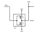
遅延反転回路DLjは、1つのインバータにより構成される。このインバータの入力には、隣接するドライバブロックDBj−1からのストローブ信号STBj−1が入力される。そして、遅延反転回路DLjは、ストローブ信号STBj−1を遅延させ、かつ反転させた遅延反転ストローブ信号DSTBjを生成する。出力制御回路OCjには、ストローブ信号STBj−1又は遅延反転ストローブ信号DSTBjが、ストローブ信号STBjとして出力される。 The delay inversion circuit DL j is configured by one inverter. The strobe signal STB j−1 from the adjacent driver block DB j−1 is input to the input of this inverter. Then, the delay inversion circuit DL j delays the strobe signal STB j−1 and generates a delayed inversion strobe signal DSTB j . The output control circuit OC j, the strobe signal STB j-1 or delay inverting strobe signal DSTB j is output as a strobe signal STB j.
図4に、図3の遅延反転回路DLjの説明図を示す。 FIG. 4 is an explanatory diagram of the delay inverting circuit DL j shown in FIG.
図4に示すとおり、ドライバブロックDBjの遅延反転回路DLjの入力には、隣接するドライバブロックDBj−1からのストローブ信号STBj−1が入力される。そして、遅延反転回路DLjは、ストローブ信号STBj−1を遅延させ、かつ反転させた遅延反転ストローブ信号DSTBjを出力する。隣接するドライバブロックDBj+1には、遅延反転ストローブ信号DSTBjが、ストローブ信号STBjとして出力される。 As shown in FIG. 4, the input of the delay inverting circuit DL j driver block DB j, the strobe signal STB j-1 from the driver block DB j-1 adjacent is input. Then, the delay inversion circuit DL j delays the strobe signal STB j−1 and outputs the inverted delay inversion strobe signal DSTB j . The delayed inverted strobe signal DSTB j is output as the strobe signal STB j to the adjacent driver block DB j + 1 .
遅延反転回路DLjは、1つのインバータで構成され、このインバータは、たとえば、PおよびNの型のトランジスタ(CMOSトランジスタ)で構成される。遅延反転回路DLjを構成するP型のトランジスタの能力(電流駆動能力)は、フリップフロップDFF及び/又はラッチLTを構成する少なくとも1つのP型のトランジスタの能力より低い。また、遅延反転回路DLjを構成するN型のトランジスタの能力は、フリップフロップDFF及び/又はラッチLTを構成する少なくとも1つのN型のトランジスタの能力より低い。
なお、遅延反転回路DLjの能力が低く設定される程、遅延反転回路DLjは、ストローブ信号STBj−1を、より遅延させることができる。
Delay inversion circuit DL j is formed of one inverter, and this inverter is formed of, for example, P and N type transistors (CMOS transistors). The capability (current driving capability) of the P-type transistor constituting the delay inverting circuit DL j is lower than the capability of at least one P-type transistor constituting the flip-flop DFF and / or the latch LT. Further, the capability of the N-type transistor constituting the delay inverting circuit DL j is lower than the capability of the at least one N-type transistor constituting the flip-flop DFF and / or the latch LT.
Note that the delay inversion circuit DL j can further delay the strobe signal STB j−1 as the capability of the delay inversion circuit DL j is set lower.
以下、1つのインバータで構成される遅延反転回路DLjの遅延量を、たとえば0.1[ns]に設定する1例を説明する。たとえば、遅延反転回路DLjのP型のトランジスタのチャネル長およびチャネル幅がそれぞれLp1(=0.8[μm])およびWp1(=12[μm])であり、N型のトランジスタのチャネル長およびチャネル幅がそれぞれLn1(=0.8[μm])およびWn1(=6[μm])である。 Hereinafter, an example in which the delay amount of the delay inverting circuit DL j configured by one inverter is set to, for example, 0.1 [ns] will be described. For example, the channel length and the channel width of the P-type transistor of the delay inverting circuit DL j are Lp1 (= 0.8 [μm]) and Wp1 (= 12 [μm]), respectively, and the channel length of the N-type transistor and The channel widths are Ln1 (= 0.8 [μm]) and Wn1 (= 6 [μm]), respectively.
ところで、遅延反転回路DLjは、偶数個のインバータで構成される遅延回路で、置き換えることも考えられる。この遅延回路は、未公開の日本出願である、特願2006−347012号に述べられている。未公開の遅延回路では、少なくとも2個のインバータが必要となる。
以下、2個のインバータで構成される未公開の遅延回路の遅延量を、たとえば0.1[ns]に設定する1例を説明する。たとえば、未公開の遅延回路の各P型のトランジスタのチャネル長およびチャネル幅がそれぞれLp2(=0.8[μm])およびWp2(=24[μm])であり、N型のトランジスタのチャネル長およびチャネル幅がそれぞれLn2(=0.8[μm])およびWn2(=12[μm])である。
したがって、同じ遅延量を設定する場合には、遅延反転回路DLjは、未公開の遅延回路よりも小さいサイズを有する。また、遅延反転回路DLjの1つインバータは、未公開の遅延回路の1つのインバータと比較しても、小さいサイズを有するので、遅延反転回路DLjの小サイズ化効果は、大きい。
By the way, the delay inverting circuit DL j may be replaced with a delay circuit composed of an even number of inverters. This delay circuit is described in Japanese Patent Application No. 2006-347012, an unpublished Japanese application. In an undisclosed delay circuit, at least two inverters are required.
Hereinafter, an example in which the delay amount of an undisclosed delay circuit including two inverters is set to, for example, 0.1 [ns] will be described. For example, the channel length and channel width of each P-type transistor of the undisclosed delay circuit are Lp2 (= 0.8 [μm]) and Wp2 (= 24 [μm]), respectively, and the channel length of the N-type transistor The channel widths are Ln2 (= 0.8 [μm]) and Wn2 (= 12 [μm]), respectively.
Therefore, when setting the same delay amount, the delay inverting circuit DL j has a smaller size than the undisclosed delay circuit. In addition, since one inverter of the delay inverting circuit DL j has a small size as compared with one inverter of the undisclosed delay circuit, the effect of reducing the size of the delay inverting circuit DL j is large.
なお、1つのインバータで構成される遅延反転回路DLjの遅延量を、たとえば1[ns]に設定する場合、たとえば、遅延反転回路DLjのP型およびN型のトランジスタのチャネル幅が、デザインルールの最小値(たとえば、1[μm)に固定される場合もある(Wp1(=1[μm]、Wn1(=1[μm])。この例において、遅延反転回路DLjのP型およびN型のトランジスタのチャネル長は、たとえば、Lp1(=4[μm]、Ln1(=8[μm])である。2個のインバータで構成される未公開の遅延回路の遅延量を、たとえば1[ns]に設定する場合、たとえば、未公開の遅延回路の各P型のトランジスタのチャネル長およびチャネル幅がそれぞれLp2(=2[μm])およびWp2(=1[μm])であり、N型のトランジスタのチャネル長およびチャネル幅がそれぞれLn2(=4[μm])およびWn2(=1[μm])である。このようにトランジスタのチャネル幅が、デザインルールの最小値に固定される場合、遅延反転回路DLjのゲート面積は、未公開の遅延回路のゲート面積とほぼ同じになる一方、遅延量が0.1[ns]の前述の例と比べてゲート面積が小さくなると、その他の面積(接続コンタクト、配線、トランジスタのスペースなど)の方が、ゲート面積よりも大きくなる。したがって、1つのインバータで構成される遅延反転回路DLjは、たとえば、2つのインバータで構成される未公開の遅延回路の60%程度の大きさであり、小さいサイズを有する。 When the delay amount of the delay inversion circuit DL j composed of one inverter is set to, for example, 1 [ns], for example, the channel widths of the P-type and N-type transistors of the delay inversion circuit DL j are designed. In some cases, the minimum value of the rule (for example, 1 [μm]) is fixed (Wp1 (= 1 [μm], Wn1 (= 1 [μm]). In this example, the P type and N of the delay inversion circuit DL j The channel length of the type transistor is, for example, Lp1 (= 4 [μm], Ln1 (= 8 [μm]). The delay amount of an undisclosed delay circuit composed of two inverters is, for example, 1 [ ns], for example, the channel length and channel width of each P-type transistor of the undisclosed delay circuit are Lp2 (= 2 [μm]) and Wp2 (= 1 [μm]), respectively, and N-type of The channel length and the channel width of the transistor are Ln2 (= 4 [μm]) and Wn2 (= 1 [μm]), respectively, so that when the channel width of the transistor is fixed to the minimum value of the design rule, the delay The gate area of the inverting circuit DL j is almost the same as the gate area of the undisclosed delay circuit, but when the gate area is smaller than that in the above example in which the delay amount is 0.1 [ns], the other areas ( connection contacts, wires, is more space, etc.) of the transistor is larger than the gate area. Therefore, the delay inverting circuit DL j consists of one inverter, for example, the delay unpublished composed of two inverters It is about 60% of the size of the circuit and has a small size.
図3に戻って説明を続ける。 Returning to FIG. 3, the description will be continued.
出力ドライバODjは、N型金属酸化膜半導体(Metal Oxide Semiconductor:MOS)トランジスタ(以下、単にMOSトランジスタと略す)により構成される。このMOSトランジスタのドレインが、ドライバ出力DOjとなる。ドライバブロックDB1〜DBNの出力ドライバOD1〜ODNを構成するMOSトランジスタのソースには、接地電源電圧GNDが供給される。出力ドライバODjを構成するMOSトランジスタのゲートには、出力制御回路OCjからの出力制御信号cntjが供給される。図3では、出力制御信号cntjにより、出力ドライバODjを構成するMOSトランジスタのソース・ドレイン間が電気的に導通することで、ドライバ出力DOjが接地電源電圧GNDに設定される。
The output driver OD j is configured by an N-type metal oxide semiconductor (MOS) transistor (hereinafter simply referred to as a MOS transistor). The drain of this MOS transistor becomes the driver output DOj. The source of the MOS transistors constituting the
ドライバブロックDBjは、ドライバブロックDBj−1からのストローブ信号をそのまま、又はドライバブロックDBj−1からのストローブ信号を遅延させ、かつ反転させた遅延反転ストローブ信号を、隣接するドライバブロックDBj+1に供給する。 Driver block DB j is directly a strobe signal from the driver block DB j-1, or driver block DB delays the strobe signal from the j-1, and the delayed inverted strobe signal obtained by inverting the adjacent driver block DB j + 1 To supply.
出力制御回路OCjは、隣接するドライバブロックDBj−1からのストローブ信号STBj−1、又は該ストローブ信号を遅延させ、かつ反転させた遅延ストローブ信号DSTBjと、ドライバブロックDBjに対応した画素データ(ラッチLTjにラッチされた画素データ)とに基づいて、出力制御信号cntjを生成する。 The output control circuit OC j is the strobe signal STB j-1 from the driver block DB j-1 adjacent, or delaying the strobe signal, and the delayed strobe signal DSTB j obtained by inverting, corresponding to the driver block DB j An output control signal cnt j is generated based on the pixel data (pixel data latched in the latch LT j ).
図5及び図6に、図3のサーマルヘッドドライバ30の動作例のタイミング図を示す。
FIG. 5 and FIG. 6 are timing charts of an operation example of the
図5は、シフトレジスタを構成するフリップフロップDFF1〜DFFNにシリアルデータSIとして入力された画像データが格納されるタイミングを示す。クロック信号CLKに同期してシリアルに画像データP1、P2、P3、・・・・、PNがシリアルデータSIとして入力される。例えば画像データP1はドライバブロックDB1のドライバ出力DO1に対応し、画像データP2はドライバブロックDB2のドライバ出力DO2に対応し、・・・、画像データPNはドライバブロックDBNのドライバ出力DONに対応している。フリップフロップDFF1は、クロック信号CLKの変化点に同期してシリアルデータSIの画像データP1を取り込む。フリップフロップDFF2は、クロック信号CLKの変化点に同期してシリアルデータSIの画像データP2を取り込む。フリップフロップDFFNは、クロック信号CLKの変化点に同期してシリアルデータSIの画像データPNを取り込む。 FIG. 5 shows the timing at which image data input as serial data SI is stored in the flip-flops DFF 1 to DFF N constituting the shift register. Image data P1, P2, P3,..., PN are serially input as serial data SI in synchronization with the clock signal CLK. For example, the image data P1 corresponds to the driver output DO1 of the driver blocks DB 1, the image data P2 corresponds to the driver output DO2 driver block DB 2, ···, the image data PN is the driver output DON of the driver block DB N It corresponds. The flip-flop DFF 1 takes in the image data P1 of the serial data SI in synchronization with the changing point of the clock signal CLK. Flip-flop DFF 2 captures the image data P2 of the serial data SI synchronously with the change point of the clock signal CLK. The flip-flop DFF N takes in the image data PN of the serial data SI in synchronization with the changing point of the clock signal CLK.
図6は、ラッチLT1〜LTNに保持された画像データを用いたドライバ出力のタイミングを示す。図6では、ドライバ出力DO1、DO2を示すが、他のドライバ出力も同様である。 FIG. 6 shows driver output timings using image data held in the latches LT 1 to LT N. FIG. 6 shows the driver outputs DO1 and DO2, but the other driver outputs are the same.
ラッチ信号LATがHレベルのときに、フリップフロップDFF1に保持された画像データP1がラッチLT1に取り込まれる。このとき、同様にフリップフロップDFF2〜DFFNに保持された画像データP2〜PNがラッチLT2〜LTNに取り込まれる。従って、ラッチ信号LATにより、1ライン分の画像データP1〜PNをラッチLT1〜LTNに取り込むことができる。 When the latch signal LAT is at the H level, image data P1 that is held in the flip-flop DFF 1 is taken into the latch LT 1. At this time, similarly the image data P2~PN held by the flip-flop DFF 2 ~DFF N is taken into the latch LT 2 to LT N. Accordingly, the latch signal LAT, can capture image data P1~PN of one line to latch LT 1 to LT N.
図3では、ストローブ信号STB0がストローブ信号STB1としてそのまま出力される。遅延反転回路DL2は、ストローブ信号STB1を遅延させ、かつ反転させた遅延反転ストローブ信号DSTB2を出力する。遅延反転ストローブ信号DSTB2は、ストローブ信号STB2として、隣接するドライバブロックDB3に対して出力される。 In FIG. 3, the strobe signal STB 0 is output as it is as the strobe signal STB 1 . The delay inversion circuit DL 2 delays the strobe signal STB 1 and outputs a delayed inversion strobe signal DSTB 2 that is inverted. The delayed inversion strobe signal DSTB 2 is output as the strobe signal STB 2 to the adjacent driver block DB 3 .
ここで、図3に示すように、ドライバブロックDB1の出力ドライバOD1は、ストローブ信号STB1とラッチLT1に保持された画像データP1とに基づいて、ドライバ出力DO1に接続されるサーマル抵抗素子を駆動することができる。より具体的には、ラッチLT1に保持された画像データP1が「1」、且つストローブ信号STB1がHレベルのとき、出力制御信号cnt1がHレベルとなり、出力ドライバOD1のMOSトランジスタのドレインは接地電源電圧GNDに設定される。従って、出力ドライバOD1に接続されるサーマル抵抗素子に電流が流れる。 Here, as shown in FIG. 3, the output driver OD 1 of driver block DB 1 is thermal resistance on the basis of the image data P1 held in the strobe signal STB 1 and the latch LT 1, is connected to the driver output DO1 The element can be driven. More specifically, the image data P1 stored in the latch LT 1 is "1", and the strobe signal STB 1 are at H level, the output control signal cnt 1 becomes H level, the output driver OD 1 of the MOS transistor The drain is set to the ground power supply voltage GND. Accordingly, current flows through the thermal resistance element connected to the output driver OD 1.
一方、画像データP1が「0」、又はストローブ信号STB1がLレベルのとき、出力制御信号cnt1がLレベルのままで、出力ドライバOD1のMOSトランジスタのドレイン・ソース間は電気的に遮断される。その結果、出力ドライバOD1に接続されるサーマル抵抗素子に電流が流れない。 On the other hand, when the image data P1 is “0” or the strobe signal STB 1 is at L level, the output control signal cnt 1 remains at L level and the drain and source of the MOS transistor of the output driver OD 1 are electrically cut off. Is done. As a result, current does not flow through the thermal resistance element connected to the output driver OD 1.
また図3に示すように、ドライバブロックDB2の出力ドライバOD2は、ストローブ信号STB2とラッチLT2に保持された画像データP2とに基づいて、ドライバ出力DO2に接続されるサーマル抵抗素子を駆動することができる。なお、後述するように、ラッチLT2の出力は、負論理であり、保持された画像データP2が反転されたデータが、ドライバ出力DO2に供給される。
より具体的には、ラッチLT2に保持された画像データP2が「1」(したがって、ラッチLT2の出力が「0」)、且つストローブ信号STB2がLレベル(すなわち、ストローブ信号STB1がHレベル)のとき、出力制御信号cnt2がHレベルとなり、出力ドライバOD2のMOSトランジスタのドレインは接地電源電圧GNDに設定される。従って、出力ドライバOD2に接続されるサーマル抵抗素子に電流が流れる。
As shown in FIG. 3, the output driver OD 2 of the driver block DB 2 is a thermal resistance element connected to the driver output DO 2 based on the strobe signal STB 2 and the image data P 2 held in the latch LT 2. Can be driven. As described below, the output of the latch LT 2 is a negative logic, data image data P2 held is inverted is supplied to the driver output DO 2.
More specifically, the image data P2 held in the latch LT 2 is "1" (therefore, the output of the latch LT 2 is "0"), and the strobe signal STB 2 is L-level (i.e., the strobe signal STB 1 Output control signal cnt 2 becomes H level, and the drain of the MOS transistor of the output driver OD 2 is set to the ground power supply voltage GND. Accordingly, current flows through the thermal resistance element connected to the output driver OD 2.
一方、画像データP2が「0」(したがって、ラッチLT2の出力が「1」)、又はストローブ信号STB2がHレベル(すなわち、ストローブ信号STB1がLレベル)のとき、出力制御信号cnt2がLレベルのままで、出力ドライバOD2のMOSトランジスタのドレイン・ソース間は電気的に遮断される。その結果、出力ドライバOD2に接続されるサーマル抵抗素子に電流が流れない。 On the other hand, when the image data P2 is “0” (therefore, the output of the latch LT 2 is “1”) or the strobe signal STB 2 is at the H level (that is, the strobe signal STB 1 is at the L level), the output control signal cnt 2 There remains L-level, between the drain and source of the MOS transistor of the output driver OD 2 is cut off electrically. As a result, current does not flow through the thermal resistance element connected to the output driver OD 2.
そして、ストローブ信号STB1、STB2の遅延差によって、ドライバ出力DO1、DO2も遅延差が生じる。その結果、ドライバ出力DO1に接続されるサーマル抵抗素子に流れる電流I1と、ドライバ出力DO2に接続されるサーマル抵抗素子に流れる電流I2とに時間差が生じる。図6では、ドライバ出力DO1、DO2について説明したが、他のドライバ出力についても時間差を設けることで、発生するサージ電圧を抑えることにより電源電圧VHのレベルの変動と発生ノイズを抑えることが可能となる。 Due to the delay difference between the strobe signals STB 1 and STB 2 , the driver outputs DO 1 and DO 2 also have a delay difference. As a result, there is a time difference between the current I1 flowing through the thermal resistance element connected to the driver output DO1 and the current I2 flowing through the thermal resistance element connected to the driver output DO2. Although the driver outputs DO1 and DO2 have been described with reference to FIG. 6, it is possible to suppress fluctuations in the level of the power supply voltage VH and generated noise by suppressing the generated surge voltage by providing a time difference for the other driver outputs. Become.
好ましくは、ドライバ出力DO1〜DONのそれぞれが互いに異なるタイミングで、サーマル抵抗素子に電流を流す、あるいは遮断することで、サージ電圧を最小に抑えることができる。しかし、1ライン分の遅延時間に制約がある場合には、複数のタイミングのいずれかでドライバ出力DO1〜DONに接続されるサーマル抵抗素子に流れる電流を流す、あるいは遮断するタイミングをずらすようにしてもよい。この場合でも、サージ電圧を低減させることが可能となる。 Preferably, the surge voltage can be minimized by flowing or interrupting the current through the thermal resistance element at different timings of the driver outputs DO1 to DON. However, when there is a restriction on the delay time for one line, the current flowing through or shutting off the current flowing through the thermal resistance elements connected to the driver outputs DO1 to DON is shifted at any one of a plurality of timings. Also good. Even in this case, the surge voltage can be reduced.
2.1 ドライバブロックDBの構成例
なお、サーマルヘッドドライバ30の各ドライバブロックは、図3の構成に限定されるものではない。
2.1 Configuration Example of Driver Block DB Each driver block of the
図7は、ドライバブロックDB内の出力制御回路OC及びラッチLTを構成する第1の例を示す。
上述のとおり、複数のドライバブロックDB1〜DBNは、遅延反転回路DLを含まない第1のドライバブロックDB1と、遅延反転回路DLを含む第2のドライバブロックDB2とで、構成することができる。
図7に示されるドライバブロックDBJは、第1のドライバブロックDB1に属する。すなわち、図7に示されるドライバブロックDBJは、隣接するドライバブロックDBJ−1からのストローブ信号STBJ−1をそのまま、ストローブ信号STBJとして出力する。なお、図7に示されるドライバブロックDBJが、初段のドライバブロックDB1である場合、ドライバブロックDB1は、ストローブ信号STB0をそのまま、ストローブ信号STB1として出力する。
図7に示されるドライバブロックDBJにおいて、ストローブ信号STBJが正論理である場合、ラッチLTJの出力は、正論理であり、出力ドライバOCJは、AND回路(論理積回路)で構成される。なお、AND回路OCJは、NAND回路とインバータとで構成することができる。
FIG. 7 shows a first example configuring the output control circuit OC and the latch LT in the driver block DB.
As described above, the plurality of driver blocks DB 1 to DB N can be configured by the first
The driver block DB J shown in FIG. 7 belongs to the first driver block DB1. That is, the driver block DB J shown in FIG. 7 outputs the strobe signal STB J-1 from the adjacent driver block DB J-1 as it is as the strobe signal STB J. When the driver block DB J shown in FIG. 7 is the first-stage driver block DB 1 , the driver block DB 1 outputs the strobe signal STB 0 as it is as the strobe signal STB 1 .
In the driver block DB J shown in FIG. 7, when the strobe signal STB J is positive logic, the output of the latch LT J is positive logic, and the output driver OC J is composed of an AND circuit (logical product circuit). The The AND circuit OC J can be composed of a NAND circuit and an inverter.
図8は、ドライバブロックDB内の出力制御回路OC及びラッチLTを構成する第2の例を示す。
図8に示されるドライバブロックDBJも、第1のドライバブロックDB1に属する。すなわち、図8に示されるドライバブロックDBJは、隣接するドライバブロックDBJ−1からのストローブ信号STBJ−1をそのまま、ストローブ信号STBJとして出力する。なお、図8に示されるドライバブロックDBJが、初段のドライバブロックDB1であってもよい。また、図8に示されるドライバブロックDBJは、複数のドライバブロックDB2〜DBNのいずれかであってもよい。
図8に示されるドライバブロックDBJにおいて、ストローブ信号STBJが負論理である場合、ラッチLTJの出力は、負論理であり、出力ドライバOCJは、NOR回路(論理和回路)で構成される。
FIG. 8 shows a second example configuring the output control circuit OC and the latch LT in the driver block DB.
The driver block DB J shown in FIG. 8 also belongs to the first driver block DB1. That is, the driver block DB J shown in FIG. 8 outputs the strobe signal STB J-1 from the adjacent driver block DB J-1 as it is as the strobe signal STB J. Note that the driver block DB J shown in FIG. 8 may be the first-stage driver block DB 1 . The driver block DB J shown in FIG. 8, may be any of a plurality of driver blocks DB 2 to DB N.
In the driver block DB J shown in FIG. 8, when the strobe signal STB J is negative logic, the output of the latch LT J is negative logic, and the output driver OC J is composed of a NOR circuit (OR circuit). The
図9は、ドライバブロックDB内の出力制御回路OC及びラッチLTを構成する第3の例を示す。
図9に示されるドライバブロックDBJは、第2のドライバブロックDB2に属する。すなわち、図9に示されるドライバブロックDBJは、隣接するドライバブロックDBJ−1からのストローブ信号STBJ−1を遅延反転回路DLJにより遅延させ、かつ反転させて、ストローブ信号STBJとして出力する。なお、図7に示されるドライバブロックDBJが、初段のドライバブロックDB1であり、図9に示されるドライバブロックDBJが、その次段のドライバブロックDB2である場合、図9において、隣接するドライバブロックDBJ−1からのストローブ信号STBJ−1は、正論理であり、したがって、ドライバブロックDBJからのストローブ信号STBJは、負論理である。
図9に示されるドライバブロックDBJにおいて、ストローブ信号STBJが負論理である場合、ラッチLTJの出力は、負論理であり、出力ドライバOCJは、NOR回路(論理和回路)で構成される。
FIG. 9 shows a third example configuring the output control circuit OC and the latch LT in the driver block DB.
The driver block DB J shown in FIG. 9 belongs to the second driver block DB2. That is, the driver block DB J shown in FIG. 9, a strobe signal STB J-1 from the driver block DB J-1 adjacent delayed by the delay inverting circuit DL J, and inverts, the output as a strobe signal STB J To do. When the driver block DB J shown in FIG. 7 is the first stage driver block DB 1 and the driver block DB J shown in FIG. 9 is the next stage driver block DB 2 , strobe signal STB J-1 from the driver block DB J-1 to are positive logic, therefore, the strobe signal STB J from driver block DB J, is a negative logic.
In the driver block DB J shown in FIG. 9, when the strobe signal STB J is negative logic, the output of the latch LT J is negative logic, and the output driver OC J is configured by a NOR circuit (OR circuit). The
図10は、ドライバブロックDB内の出力制御回路OC及びラッチLTを構成する第4の例を示す。
図10に示されるドライバブロックDBJも、第2のドライバブロックDB2に属する。すなわち、図10に示されるドライバブロックDBJは、隣接するドライバブロックDBJ−1からのストローブ信号STBJ−1を遅延反転回路DLJにより遅延させ、かつ反転させて、ストローブ信号STBJとして出力する。なお、図7に示されるドライバブロックDBJが、初段のドライバブロックDB1であり、図9に示されるドライバブロックDBJが、その次段のドライバブロックDB2であり、図10に示されるドライバブロックDBJが、その次段のドライバブロックDB3である場合、図10において、隣接するドライバブロックDBJ−1からのストローブ信号STBJ−1は、負論理であり、したがって、ドライバブロックDBJからのストローブ信号STBJは、正論理である。
図10に示されるドライバブロックDBJにおいて、ストローブ信号STBJが正論理である場合、ラッチLTJの出力は、正論理であり、出力ドライバOCJは、AND回路(論理積回路)で構成される。
FIG. 10 shows a fourth example configuring the output control circuit OC and the latch LT in the driver block DB.
The driver block DB J shown in FIG. 10 also belongs to the second driver block DB2. That is, the driver block DB J shown in FIG. 10, a strobe signal STB J-1 from the driver block DB J-1 adjacent delayed by the delay inverting circuit DL J, and inverts, the output as a strobe signal STB J To do. The driver block DB J shown in FIG. 7 is the first-stage driver block DB 1 , the driver block DB J shown in FIG. 9 is the next-stage driver block DB 2 , and the driver shown in FIG. If block DB J is its next driver block DB 3, 10, the strobe signal STB J-1 from the driver block DB J-1 adjacent is a negative logic, therefore, the driver block DB J The strobe signal STB J from is positive logic.
In the driver block DB J shown in FIG. 10, when the strobe signal STB J is positive logic, the output of the latch LT J is positive logic, and the output driver OC J is composed of an AND circuit (logical product circuit). The
ところで、上述のとおり、好ましくは、ドライバ出力DO1〜DONのそれぞれが互いに異なるタイミングで、サーマル抵抗素子に電流を流すことで、サージ電圧を最小に抑えることができる。すなわち、ドライバブロックDB1〜DBNのそれぞれにおいて、ストトーブ信号STB1〜STBNは、順次に遅延されることが好ましい。しかしながら、サーマルヘッドドライバ30の中を流れるストローブ信号の1ラインの総遅延時間(ストローブ信号STBNとストローブ信号STB0との間の遅延量)に制約がある場合には、複数のタイミングのいずれかでドライバ出力DO1〜DONに接続されるサーマル抵抗素子に流れる電流を流すタイミングをずらすようにしてもよい。すなわち、ドライバブロックDB1〜DBNの中から遅延反転回路DLを含むドライバブロックを選択してもよい。
なお、図2のサーマルヘッド20を参照すれば、サーマルヘッド20は、第1〜第Mのサーマルヘッドドライバ301〜30Mを備える。したがって、第1〜第Mのサーマルヘッドドライバ301〜30Mのそれぞれにおいて、ドライバブロックDB1〜DBNの中から遅延反転回路DLを含むドライバブロックを選択してもよい。
By the way, as described above, preferably, the surge voltages can be minimized by flowing currents through the thermal resistance elements at different timings of the driver outputs DO1 to DON. That is, it is preferable that the stove signals STB 1 to STB N are sequentially delayed in each of the driver blocks DB 1 to DB N. However, if there are restrictions on 1 total delay time of the line the strobe signals flowing through the thermal head driver 30 (the delay amount between the strobe signal STB N and the strobe signal STB 0) is one of a plurality of timing Thus, the timing of flowing the current flowing through the thermal resistance elements connected to the driver outputs DO1 to DON may be shifted. That may be selected driver block including a delay inverting circuit DL from the driver blocks DB 1 to DB N.
Referring to the
具体的には、図3に示される1つのサーマルヘッドドライバ30の中を流れるストローブ信号の1ラインの総遅延時間(DT)は、1ライン分の画素データを取り込む周期より短く設定される。1つの遅延反転回路DL(すなわち、1つのインバータ)によって、ストローブ信号を遅延させることが可能な遅延量をD1とすると、DT/(N−1)≧D1である場合、ドライバブロックDB1を除き、ドライバブロックDB2〜DBNのそれぞれが、遅延反転回路DLを備えることができる。
言い換えれば、DT/(N−1)<D1である場合、ドライバブロックDB2〜DBNのすべては、遅延反転回路DLを備えることができず、ドライバブロックDB2〜DBNの一部が、遅延反転回路DLを備えることができる。
Specifically, the total delay time (DT) of one line of the strobe signal that flows in one
In other words, if a DT / (N-1) < D1, all of the driver block DB 2 to DB N, can not be provided with the delay inverting circuit DL, a part of the driver block DB 2 to DB N, A delay inversion circuit DL can be provided.
DT/(N−1)<D1である場合、ドライバブロックDB1〜DBNの中で、好ましくは、ドライバブロックDB2〜DBNの中で、遅延反転回路DLを備えることができるドライバブロックの最大の個数は、DTをD1で除算したときの商に等しい数である。したがって、DTをD1で除算したときの商を超えない数のドライバブロックを選択し、選択されたドライバブロックのそれぞれは、遅延反転回路DLを備え、残りのドライバブロックは、遅延反転回路DLを備えない。 When DT / (N−1) <D1, among the driver blocks DB 1 to DB N , preferably, among the driver blocks DB 2 to DB N , the driver block that can include the delay inverting circuit DL The maximum number is a number equal to the quotient when DT is divided by D1. Therefore, a number of driver blocks that do not exceed the quotient obtained by dividing DT by D1 are selected, and each of the selected driver blocks includes a delay inversion circuit DL, and the remaining driver blocks include a delay inversion circuit DL. Absent.
たとえば、図3において、偶数番目のドライバブロックのみが遅延反転回路DLを備える場合、1番目のドライバブロックDB1は、図7のドライバブロックDBで構成され、2番目のドライバブロックDB2は、図9のドライバブロックDBで構成され、3番目のドライバブロックDB3は、図8のドライバブロックDBで構成され、4番目のドライバブロックDB4は、図10のドライバブロックDBで構成され、5番目のドライバブロックDB5は、図7のドライバブロックDBで構成される。
このように、J番目のドライバブロックDBJは、隣接するドライバブロックDBJ−1からのストローブ信号STBJ−1の論理符号に応じて、構成される。
For example, in FIG. 3, when only the even-numbered driver block includes the delay inversion circuit DL, the first driver block DB 1 is configured by the driver block DB of FIG. 7, and the second driver block DB 2 is The third driver block DB 3 is composed of the driver block DB of FIG. 8, the fourth driver block DB 4 is composed of the driver block DB of FIG. 10, and the fifth driver block DB 3 is composed of the driver block DB of FIG. The driver block DB 5 includes the driver block DB shown in FIG.
Thus, the J-th driver block DB J is configured according to the logical code of the strobe signal STB J-1 from the adjacent driver block DB J-1 .
図11は、図3に示されるラッチLTjの具体例を示す。
図11に示されるように、ラッチLTjは、たとえば、5個のN型のトランジスタN11〜N15と、5個のP型のトランジスタP11〜P15とで、構成される。トランジスタP12、N12のゲートは、フリップフロップDFFj内で保持するデータを受け取る。トランジスタP13、N13のドレインは、ラッチ信号(LAT)または反転ラッチ信号(XLAT)の変化タイミングに同期して、ラッチLTj内で保持するデータを出力制御回路OCjに出力する。トランジスタP13、N13のドレインは、正論理出力である。また、図11に示されるように、ラッチLTjは、トランジスタP12、N12のドレインにおいて、負論理に従って出力することができる。
したがって、図7〜図10に示されるラッチLTjの出力の論理符号に応じて、出力制御回路OCjは、トランジスタP13、N13のドレイン、または、トランジスタP12、N12のドレインと接続される。
FIG. 11 shows a specific example of the latch LT j shown in FIG.
As shown in FIG. 11, the latch LT j is composed of, for example, five N-type transistors N11 to N15 and five P-type transistors P11 to P15. The gates of the transistors P12 and N12 receive data held in the flip-flop DFF j . The drains of the transistors P13 and N13 output the data held in the latch LT j to the output control circuit OC j in synchronization with the change timing of the latch signal (LAT) or the inverted latch signal (XLAT). The drains of the transistors P13 and N13 are positive logic outputs. Further, as shown in FIG. 11, the latch LT j can output in accordance with negative logic at the drains of the transistors P12 and N12.
Therefore, the output control circuit OC j is connected to the drains of the transistors P13 and N13 or the drains of the transistors P12 and N12 according to the logic sign of the output of the latch LT j shown in FIGS.
3. 電子機器
次に、本実施形態におけるサーマルヘッドが適用される電子機器としてのプリンタ装置(サーマルプリンタ)と、該プリンタ装置が適用される印刷システムについて説明する。
3. Next, a printer apparatus (thermal printer) as an electronic apparatus to which the thermal head according to the present embodiment is applied, and a printing system to which the printer apparatus is applied will be described.
図12に、本実施形態におけるプリンタ装置の説明図を示す。 FIG. 12 is an explanatory diagram of the printer apparatus according to this embodiment.
図12は、本実施形態におけるプリンタ装置120の縦断面の主要部分のみを示す縦断面図である。プリンタ装置120内には、感熱紙がロール紙122としてセットされる様に構成されている。ロール紙122の印刷対象部分は、所与の紙送り機構(紙送り手段)により1ラインずつ紙送り方向123の方向に送り出される。そして、この印刷対象部分は、ハウジング124内で印刷ヘッド125の方に導かれる。印刷ヘッド125は、図2のサーマルヘッド20を搭載する。ロール紙122の印刷対象部分が、印刷ヘッド125及びプラテン126の間を通過する際に、印刷ヘッド125により該印刷対象部分に所定の印刷が行われる。
FIG. 12 is a longitudinal sectional view showing only the main part of the longitudinal section of the
紙送り機構は、印刷対象部分を更に紙送り方向123に送り出し、カッター127によりロール紙122が切断されて、切断後の用紙がレシート128として取り出し可能となる。
The paper feed mechanism further feeds the print target portion in the
またハウジング124内には、印刷ヘッド125の前段に、用紙エンドセンサ129が設けられており、ロール紙122が紙送り方向123に送られる際にロール紙122の端を検知できる。
In the
本実施形態におけるプリンタ装置によれば、サージ電圧を低減でき、ノイズによる誤動作を防止できる。 According to the printer device in the present embodiment, surge voltage can be reduced and malfunction due to noise can be prevented.
図13に、図12のプリンタ装置120が適用される印刷システムの構成例を示す。
FIG. 13 shows a configuration example of a printing system to which the
本実施形態における印刷システム130は、ホストコンピュータ132(広義には制御部)と、レシート128等を発行するプリンタ装置120とを含む。ホストコンピュータ132は、本体134と、表示装置136と、キーボード137と、ポインティングデバイスとしてのマウス138とを含む。
The
図14に、図13のホストコンピュータ132の構成例のブロック図を示す。
FIG. 14 is a block diagram showing a configuration example of the
ホストコンピュータ132では、CPU(Central Processing Unit)141に、バスライン142を介して、プログラムデータ等が格納されたROM(Read Only Memory)143、データ処理の作業エリアや印刷データがバッファリングされるRAM(Random Access Memory)144、プリンタ装置120に印刷データや印刷コマンド等を送信する通信インタフェース145、表示装置136を駆動制御して表示データに対応する文字等を表示させるディスプレイコントローラ146、キーボード137から入力キーに対応するキー信号を取り込むキーボードコントローラ147、マウス138とのデータ等のやり取りを制御するマウスコントローラ148が接続されている。また、プリンタ装置120は、通信インタフェース145からの印刷データ等を受信する通信インタフェース149を含む。
In the
CPU141は、ROM143又はRAM144に格納されたプログラムに従って所定の印刷処理を実行し、印刷データをRAM144に展開したり、RAM144の印刷データを、通信インタフェース145を介してプリンタ装置120に転送したりすることができる。
The
本実施形態における印刷システムによれば、サージ電圧を低減でき、ノイズによる誤動作を防止できる。 According to the printing system of the present embodiment, surge voltage can be reduced and malfunction due to noise can be prevented.
なお、本発明は上述した実施の形態に限定されるものではなく、本発明の要旨の範囲内で種々の変形実施が可能である。例えば、遅延反転回路DLjがドライバブロックDBj内になくてもよい。 The present invention is not limited to the above-described embodiment, and various modifications can be made within the scope of the gist of the present invention. For example, the delay inverting circuit DL j may not be in the driver block DB j .
また、本発明のうち従属請求項に係る発明においては、従属先の請求項の構成要件の一部を省略する構成とすることもできる。また、本発明の1の独立請求項に係る発明の要部を、他の独立請求項に従属させることもできる。 In the invention according to the dependent claims of the present invention, a part of the constituent features of the dependent claims can be omitted. Moreover, the principal part of the invention according to one independent claim of the present invention can be made dependent on another independent claim.
20 サーマルヘッド、 22 セラミック板、
301〜30M 第1〜第Mのサーマルヘッドドライバ、
30 サーマルヘッドドライバ、 120 プリンタ装置、122 ロール紙、
123 紙送り方向、 124 ハウジング、 125 印刷ヘッド、
126 プラテン、 127 カッター、 128 レシート、130 印刷システム、
132 ホストコンピュータ、 134 本体、 136 表示装置、
137 キーボード、 138 マウス、 CLK クロック信号、
DB1〜DBN ドライバブロック、 DFF1〜DFFN フリップフロップ、
DL1〜DLN 遅延反転回路、 DO1〜DON ドライバ出力、
DSTB1〜DSTBN 遅延ストローブ信号、 LT1〜LTN ラッチ、
LAT ラッチ信号、 OC1〜OCN 出力制御回路、
OD1〜ODN 出力ドライバ、 STB0〜STBN ストローブ信号、
SI シリアルデータ
20 thermal head, 22 ceramic plate,
30 1 to 30 M first to M- th thermal head drivers,
30 thermal head driver, 120 printer device, 122 roll paper,
123 paper feed direction, 124 housing, 125 print head,
126 platen, 127 cutter, 128 receipt, 130 printing system,
132 host computer, 134 main body, 136 display device,
137 keyboard, 138 mouse, CLK clock signal,
DB 1 to DB N driver block, DFF 1 to DFF N flip-flop,
DL 1 through DL N delay inverting circuit, DO1~DON driver output,
DSTB 1 to DSTB N delay strobe signal, LT 1 to LT N latch,
LAT latch signal, OC 1 ~OC N output control circuit,
OD 1 ~OD N output driver, STB 0 ~STB N strobe signals,
SI serial data
Claims (12)
各ドライバブロックが、
所与のシフト方向に画素データがシフトされるシフトレジスタを構成するフリップフロップと、
前記フリップフロップに保持された画素データをラッチするためのラッチと、
発熱素子を駆動する出力ドライバを含み、
前記複数のドライバブロックのうちの第1のドライバブロックの前記出力ドライバが、
前記第1のドライバブロックに対応した発熱素子を、ストローブ信号と前記ラッチからの第1の画素データとに基づいて駆動し、
前記複数のドライバブロックのうちの第2のドライバブロックの前記出力ドライバが、
前記第2のドライバブロックに対応した発熱素子を、ストローブ信号を遅延反転回路により遅延させ、かつ反転させた遅延反転ストローブ信号と前記ラッチからの第2の画素データとに基づいて駆動し、
前記第2のドライバブロックで、前記遅延反転回路は、1つのインバータで構成される、
前記第1のドライバブロックで、前記ストローブ信号が正論理である場合、前記ラッチの出力は、正論理であり、前記ストローブ信号が負論理である場合、前記ラッチの出力は、負論理であり、
前記第2のドライバブロックで、前記遅延反転ストローブ信号が正論理である場合、前記ラッチの出力は、正論理であり、前記遅延反転ストローブ信号が負論理である場合、前記ラッチの出力は、負論理である、サーマルヘッドドライバ。 A thermal head driver composed of a plurality of driver blocks for driving a plurality of heating elements,
Each driver block
A flip-flop constituting a shift register in which pixel data is shifted in a given shift direction;
A latch for latching pixel data held in the flip-flop;
Including an output driver that drives the heating element;
The output driver of the first driver block of the plurality of driver blocks is
Driving the heating element corresponding to the first driver block based on the strobe signal and the first pixel data from the latch ;
The output driver of a second driver block of the plurality of driver blocks is
Driving the heating element corresponding to the second driver block based on the delayed inversion strobe signal obtained by delaying and inverting the strobe signal by the delay inversion circuit and the second pixel data from the latch ;
In the second driver block, the delay inverting circuit is composed of one inverter.
In the first driver block, when the strobe signal is positive logic, the output of the latch is positive logic; when the strobe signal is negative logic, the output of the latch is negative logic;
In the second driver block, when the delayed inverted strobe signal is positive logic, the output of the latch is positive logic. When the delayed inverted strobe signal is negative logic, the output of the latch is negative. Logic, thermal head driver.
各ドライバブロックで、前記ラッチの出力が正論理である場合、出力ドライバは、論理積回路によって制御され、前記ラッチの出力が負論理である場合、出力ドライバは、論理和回路によって制御される、
サーマルヘッドドライバ。 In claim 1 ,
In each driver block, when the output of the latch is positive logic, the output driver is controlled by an AND circuit, and when the output of the latch is negative logic, the output driver is controlled by an OR circuit.
Thermal head driver.
前記1つのインバータは、第1および第2の導電型のトランジスタを含み、
前記第1の導電型の前記トランジスタの能力は、前記フリップフロップ及び/又は前記ラッチを構成する少なくとも1つのトランジスタであって、前記第1の導電型と同じ導電型の少なくとも1つのトランジスタの能力より低く、
前記第2の導電型の前記トランジスタの能力は、前記フリップフロップ及び/又は前記ラッチを構成する少なくとも1つのトランジスタであって、前記第2の導電型と同じ導電型の少なくとも1つのトランジスタの能力より低い、サーマルヘッドドライバ。 In claim 2 ,
The one inverter includes transistors of first and second conductivity types,
The capability of the transistor of the first conductivity type is the capability of at least one transistor constituting the flip-flop and / or the latch, and the capability of at least one transistor of the same conductivity type as the first conductivity type. Low,
The capability of the transistor of the second conductivity type is at least one transistor constituting the flip-flop and / or the latch, and is greater than the capability of at least one transistor of the same conductivity type as the second conductivity type. Low thermal head driver.
各ドライバブロックが、発熱素子を駆動する出力ドライバを含み、
各ドライバブロックが、
隣接するドライバブロックからのストローブ信号をそのまま、又は該ストローブ信号を遅延反転回路により遅延させ、かつ反転させて出力し、
前記複数のドライバブロックのうちの第1のドライバブロックが、
前記第1のドライバブロックに対応した発熱素子を、隣接するドライバブロックからのストローブ信号と第1の画素データとに基づいて駆動し、
前記複数のドライバブロックのうちの第2のドライバブロックが、
前記第2のドライバブロックに対応した発熱素子を、隣接するドライバブロックからのストローブ信号を遅延反転回路により遅延させ、かつ反転させた遅延反転ストローブ信号と第2の画素データとに基づいて駆動し、
前記第2のドライバブロックで、前記遅延反転回路は、1つのインバータで構成される、サーマルヘッドドライバ。 A thermal head driver composed of a plurality of driver blocks for driving a plurality of heating elements,
Each driver block includes an output driver that drives the heating element,
Each driver block
Output the strobe signal from the adjacent driver block as it is, or delay and invert the strobe signal by the delay inversion circuit,
A first driver block of the plurality of driver blocks is
Driving the heating element corresponding to the first driver block based on the strobe signal and the first pixel data from the adjacent driver block;
A second driver block of the plurality of driver blocks is
The heating element corresponding to the second driver block is driven based on the delayed inversion strobe signal and the second pixel data obtained by delaying the strobe signal from the adjacent driver block by the delay inversion circuit and inverting the strobe signal.
In the second driver block, the delay inversion circuit is a thermal head driver including one inverter.
各ドライバブロックが、発熱素子を駆動する出力ドライバを含み、
前記複数のドライバブロックのすべてが、
各ドライバブロックに対応した発熱素子を、ストローブ信号を遅延反転回路により遅延させ、かつ反転させた遅延反転ストローブ信号と画素データとに基づいて駆動し、
各ドライバブロックで、前記遅延反転回路は、1つのインバータで構成される、サーマルヘッドドライバ。 A thermal head driver composed of a plurality of driver blocks for driving a plurality of heating elements,
Each driver block includes an output driver that drives the heating element,
All of the plurality of driver blocks are
The heat generating element corresponding to each driver block is driven based on the delayed inverted strobe signal and pixel data obtained by delaying and inverting the strobe signal by the delay inverting circuit,
In each driver block, the delay inversion circuit is a thermal head driver composed of one inverter.
前記複数の発熱抵抗素子の各発熱抵抗素子の他端に各出力ドライバの出力が電気的に接続される請求項1乃至5のいずれか記載のサーマルヘッドドライバと、
を備えるサーマルヘッド。 A plurality of heating resistance elements to which a given power supply voltage is supplied at one end;
The thermal head driver according to any one of claims 1 to 5 , wherein an output of each output driver is electrically connected to the other end of each of the plurality of heating resistors.
Thermal head equipped with.
印刷用紙の印刷対象部分を紙送り手段とを含むことを特徴とする電子機器。 The thermal head driver according to any one of claims 1 to 5 ,
An electronic apparatus comprising: a printing target portion of printing paper; and paper feeding means.
印刷用紙の印刷対象部分を紙送り手段とを含むことを特徴とする電子機器。 The thermal head according to claim 6 or 7 ,
An electronic apparatus comprising: a printing target portion of printing paper; and paper feeding means.
前記電子機器に対して印刷データを供給する制御部と、
を備える印刷システム。 An electronic device according to claim 8 or 9 ,
A control unit for supplying print data to the electronic device;
A printing system comprising:
前記サーマルヘッドドライバの中を流れるストローブ信号の1ラインの総遅延時間を準備すること、
1つのドライバブロックで、1つのインバータによって、ストローブ信号を遅延させることが可能な第1の遅延量を準備すること、
前記1ラインの総遅延時間/(N−1)<前記第1の遅延量の場合、前記1ラインの総遅延時間を前記第1の遅延量で除算したときの商を超えない数のドライバブロックを前記N個のドライバブロックの中から選択すること、
前記選択されたドライバブロックのそれぞれに、ストローブ信号を遅延させ、かつ反転させた遅延反転ストローブ信号を出力する1つのインバータと、前記遅延反転ストローブ信号に基づいて制御される出力ドライバと、を配置すること、
前記選択されなかった残りのドライバブロックのそれぞれに、ストローブ信号に基づいて制御される出力ドライバを配置すること、
を含むサーマルヘッドドライバのレイアウト方法。 A thermal head driver layout method composed of N driver blocks for driving N heat generating elements,
Preparing a total delay time for one line of a strobe signal flowing through the thermal head driver;
Preparing a first delay amount capable of delaying the strobe signal by one inverter in one driver block;
If the total delay time of one line / (N-1) <the first delay amount, the number of driver blocks that does not exceed the quotient obtained by dividing the total delay time of the one line by the first delay amount Selecting from among the N driver blocks;
In each of the selected driver blocks, one inverter that delays and inverts the strobe signal and outputs a delayed inversion strobe signal and an output driver that is controlled based on the delayed inversion strobe signal are arranged. about,
Placing an output driver controlled based on a strobe signal in each of the remaining driver blocks not selected;
Layout method of thermal head driver including
M個のサーマルヘッドドライバのそれぞれを請求項11に記載の方法によってレイアウトすること、
を含むサーマルヘッドのレイアウト方法。
A thermal head layout method including M thermal head drivers,
Laying out each of the M thermal head drivers according to the method of claim 11 ;
Layout method of thermal head including
Priority Applications (1)
| Application Number | Priority Date | Filing Date | Title |
|---|---|---|---|
| JP2007275185A JP5217359B2 (en) | 2007-10-23 | 2007-10-23 | Thermal head driver, thermal head, electronic device and printing system, and thermal head driver and thermal head layout method |
Applications Claiming Priority (1)
| Application Number | Priority Date | Filing Date | Title |
|---|---|---|---|
| JP2007275185A JP5217359B2 (en) | 2007-10-23 | 2007-10-23 | Thermal head driver, thermal head, electronic device and printing system, and thermal head driver and thermal head layout method |
Publications (3)
| Publication Number | Publication Date |
|---|---|
| JP2009101585A JP2009101585A (en) | 2009-05-14 |
| JP2009101585A5 JP2009101585A5 (en) | 2010-12-09 |
| JP5217359B2 true JP5217359B2 (en) | 2013-06-19 |
Family
ID=40703874
Family Applications (1)
| Application Number | Title | Priority Date | Filing Date |
|---|---|---|---|
| JP2007275185A Expired - Fee Related JP5217359B2 (en) | 2007-10-23 | 2007-10-23 | Thermal head driver, thermal head, electronic device and printing system, and thermal head driver and thermal head layout method |
Country Status (1)
| Country | Link |
|---|---|
| JP (1) | JP5217359B2 (en) |
Families Citing this family (2)
| Publication number | Priority date | Publication date | Assignee | Title |
|---|---|---|---|---|
| JP5418201B2 (en) * | 2009-12-21 | 2014-02-19 | セイコーエプソン株式会社 | Integrated circuit device, thermal head, electronic device and output method |
| CN111703211A (en) * | 2020-06-16 | 2020-09-25 | 潮州三环(集团)股份有限公司 | Thermal printer head driving circuit with delay function |
Family Cites Families (10)
| Publication number | Priority date | Publication date | Assignee | Title |
|---|---|---|---|---|
| JPS61277224A (en) * | 1985-05-31 | 1986-12-08 | Mitsubishi Electric Corp | Thermal head driving device |
| JPH03278967A (en) * | 1990-03-28 | 1991-12-10 | Seiko Instr Inc | Thermal head |
| JPH07304201A (en) * | 1994-05-10 | 1995-11-21 | Rohm Co Ltd | Printing head drive ic |
| JP2000089729A (en) * | 1998-09-08 | 2000-03-31 | Matsushita Electric Ind Co Ltd | Liquid crystal display device, and shift register circuit used for it and its deriving method |
| JP3323138B2 (en) * | 1998-09-24 | 2002-09-09 | セイコーインスツルメンツ株式会社 | Integrated circuit for driving thermal head |
| JP3625389B2 (en) * | 1998-12-21 | 2005-03-02 | セイコーインスツル株式会社 | Integrated circuit for driving thermal head |
| JP2000246938A (en) * | 1999-02-26 | 2000-09-12 | Kyocera Corp | Recording head driving device |
| JP3891979B2 (en) * | 2002-11-21 | 2007-03-14 | 松下電器産業株式会社 | Data latch timing adjustment device |
| JP2005149313A (en) * | 2003-11-18 | 2005-06-09 | Toshiba Corp | Design method of semiconductor integrated circuit, and semiconductor integrated circuit |
| JP5309444B2 (en) * | 2006-12-25 | 2013-10-09 | セイコーエプソン株式会社 | Thermal head driver, thermal head, electronic equipment and printing system |
-
2007
- 2007-10-23 JP JP2007275185A patent/JP5217359B2/en not_active Expired - Fee Related
Also Published As
| Publication number | Publication date |
|---|---|
| JP2009101585A (en) | 2009-05-14 |
Similar Documents
| Publication | Publication Date | Title |
|---|---|---|
| TWI276547B (en) | Substrate for ink jet recording head, driving control method, ink jet recording head, and ink jet recording apparatus | |
| JP5081019B2 (en) | Element substrate for recording head, recording head, head cartridge, and recording apparatus | |
| JP4420468B2 (en) | Drive circuit, LED head, and image forming apparatus | |
| US7872491B2 (en) | Noise filter circuit, dead time circuit, delay circuit, noise filter method, dead time method, delay method, thermal head driver, and electronic instrument | |
| JP5217359B2 (en) | Thermal head driver, thermal head, electronic device and printing system, and thermal head driver and thermal head layout method | |
| US7839180B2 (en) | Noise filter circuit, noise filtering method, thermal head driver, thermal head, electronic instrument, and printing system | |
| JP5309444B2 (en) | Thermal head driver, thermal head, electronic equipment and printing system | |
| JP2007210235A (en) | Driving unit, led head, and image forming apparatus | |
| US8004548B2 (en) | Thermal head and image forming apparatus using the same | |
| JP2009126152A (en) | Element substrate, recording head, head cartridge and recording device | |
| JP5163145B2 (en) | Output circuit and electronic equipment | |
| US7125089B2 (en) | Driver device for a thermal print head | |
| JP5374879B2 (en) | Output circuit and electronic equipment | |
| JP4588429B2 (en) | Drive circuit, light emitting diode head, and image forming apparatus | |
| JP5320705B2 (en) | Output circuit and method, and thermal head driver, thermal head, electronic device, and printing system | |
| JP5239290B2 (en) | Thermal head driver, thermal head, electronic equipment and printing system | |
| JP2000198200A (en) | Liquid jet recording apparatus | |
| JP2000198188A (en) | Ink jet recording apparatus | |
| JP2018016013A (en) | Driver ic chip, drive device, print head and image formation apparatus | |
| JP6457325B2 (en) | Light emitting element driving system and image forming apparatus | |
| JP2000198198A (en) | Liquid jet recording apparatus | |
| JP5418201B2 (en) | Integrated circuit device, thermal head, electronic device and output method | |
| JP2016192682A (en) | Light emission driving circuit and image forming apparatus | |
| JP2007203665A (en) | Ink jet recording head | |
| JP2005199460A (en) | Image recording head and image recording apparatus |
Legal Events
| Date | Code | Title | Description |
|---|---|---|---|
| A521 | Written amendment |
Free format text: JAPANESE INTERMEDIATE CODE: A523 Effective date: 20101022 |
|
| A621 | Written request for application examination |
Free format text: JAPANESE INTERMEDIATE CODE: A621 Effective date: 20101022 |
|
| A977 | Report on retrieval |
Free format text: JAPANESE INTERMEDIATE CODE: A971007 Effective date: 20121024 |
|
| A131 | Notification of reasons for refusal |
Free format text: JAPANESE INTERMEDIATE CODE: A131 Effective date: 20121106 |
|
| A521 | Written amendment |
Free format text: JAPANESE INTERMEDIATE CODE: A523 Effective date: 20121221 |
|
| TRDD | Decision of grant or rejection written | ||
| A01 | Written decision to grant a patent or to grant a registration (utility model) |
Free format text: JAPANESE INTERMEDIATE CODE: A01 Effective date: 20130205 |
|
| A61 | First payment of annual fees (during grant procedure) |
Free format text: JAPANESE INTERMEDIATE CODE: A61 Effective date: 20130218 |
|
| FPAY | Renewal fee payment (event date is renewal date of database) |
Free format text: PAYMENT UNTIL: 20160315 Year of fee payment: 3 |
|
| R150 | Certificate of patent or registration of utility model |
Ref document number: 5217359 Country of ref document: JP Free format text: JAPANESE INTERMEDIATE CODE: R150 Free format text: JAPANESE INTERMEDIATE CODE: R150 |
|
| S531 | Written request for registration of change of domicile |
Free format text: JAPANESE INTERMEDIATE CODE: R313531 |
|
| R350 | Written notification of registration of transfer |
Free format text: JAPANESE INTERMEDIATE CODE: R350 |
|
| LAPS | Cancellation because of no payment of annual fees |