JP5195357B2 - Semiconductor device - Google Patents
Semiconductor device Download PDFInfo
- Publication number
- JP5195357B2 JP5195357B2 JP2008306551A JP2008306551A JP5195357B2 JP 5195357 B2 JP5195357 B2 JP 5195357B2 JP 2008306551 A JP2008306551 A JP 2008306551A JP 2008306551 A JP2008306551 A JP 2008306551A JP 5195357 B2 JP5195357 B2 JP 5195357B2
- Authority
- JP
- Japan
- Prior art keywords
- region
- semiconductor device
- trench
- oxide film
- electrode
- Prior art date
- Legal status (The legal status is an assumption and is not a legal conclusion. Google has not performed a legal analysis and makes no representation as to the accuracy of the status listed.)
- Active
Links
Images


Description
本発明は、半導体装置に関する。特に、半導体基板の表面に表面電極が配置されており、半導体基板の裏面に裏面電極が配置されている縦型の半導体装置に関する。 The present invention relates to a semiconductor device. In particular, the present invention relates to a vertical semiconductor device in which a surface electrode is disposed on the surface of a semiconductor substrate and a back electrode is disposed on the back surface of the semiconductor substrate.
近年、パワーMOS(Metal Oxide Semiconductor)等の大電流を制御できる半導体装置が開発されている。一般的に、半導体装置の高耐圧化と低オン抵抗化は、トレードオフの関係にある。このため、半導体装置では、耐圧を高めるとオン抵抗が増大し、オン抵抗を低減させると耐圧が低下する傾向が見られる。 In recent years, semiconductor devices capable of controlling a large current such as a power MOS (Metal Oxide Semiconductor) have been developed. In general, there is a trade-off between increasing the breakdown voltage and reducing the on-resistance of a semiconductor device. For this reason, in the semiconductor device, when the breakdown voltage is increased, the on-resistance increases, and when the on-resistance is decreased, the breakdown voltage tends to decrease.
特許文献1に、高耐圧化と低オン抵抗化の両立に成功したパワーMOSが記載されている。図28の(a)に、そのパワーMOS600の断面図を示す。パワーMOS600は、半導体基板224の表面に配置されている表面電極218と、半導体基板224の裏面に配置されている裏面電極226を備えており、縦型である。半導体基板224内には、ソース領域220と、ボディ領域214と、ボディコンタクト領域216と、ドリフト領域204と、ドレイン領域202が配置されている。ソース領域220は、第1導電型(n型)であり、半導体基板224の表面側に配置されており、表面電極218に導通している。ドリフト領域204は、第1導電型(n型)であり、半導体基板224の裏面側に配置されており、第1導電型(n型)のドレイン領域202を介して、裏面電極226に導通している。ボディ領域214は、第2導電型(p型)であり、ソース領域220とドリフト領域204を分離している。ボディコンタクト領域216は、第2導電型(p型)の不純物を高濃度に含有し、ボディ領域214の電位を表面電極218の電位によって安定させる。ドレイン領域202は、第1導電型(n型)の不純物を高濃度に含有し、裏面電極226との接触抵抗を低下させる。半導体基板内224には、半導体基板224の表面からソース領域220とボディ領域216を貫通してドリフト領域204に達するまで伸びているトレンチ211が配置されている。トレンチ211の深部には、絶縁膜222aが配置されている。トレンチ211の浅部には、ゲート電極212が配置されている。ゲート電極212の壁面は絶縁膜222bで被覆されている。ゲート電極212は、ボディ領域204の底面214aより深い位置まで伸びている。耐圧性能を向上させるために、トレンチ211の底面211aを囲む範囲に、第2導電型(p型)の不純物含有領域206が配置されている。不純物含有領域206は、ドリフト領域204内に配置されている。ゲート電極212は、ドリフト領域204内の浅部にのみ配置されており、ゲート電極212の底面212aと、不純物含有領域206は、絶縁膜222aで分離されている。
Patent Document 1 describes a power MOS that has successfully achieved both high breakdown voltage and low on-resistance. FIG. 28A shows a cross-sectional view of the
パワーMOS600のオフ時に発生する電界(V/cm)の深さ方向のプロファイルを調べると、図28の(b)に示すように、ゲート電極212の底面212aに一致する深さで1つ目のピークを持ち、不純物含有領域206の下部近傍の深さD1で2つ目のピークを持つことが分かる。
不純物含有領域206が形成されていないと、ゲート電極212の底面212aに一致する深さで1つだけのピークを持つ電界強度プロファイルとなる。半導体装置の耐圧は、図28(b)のハッチに示す面積が大きいほど耐圧が高い。不純物含有領域206を配置して2つのピークが形成されるようにすると、高い耐圧を確保することができる。逆に、要求される耐圧が同じであれば、不純物含有領域206を配置することによって、ドリフト領域204の不純物の濃度を上げることができる。ドリフト領域204の不純物の濃度を上げることができれば、パワーMOS600のオン抵抗が低下する。パワーMOS600は、不純物含有領域204を備えていることによって、必要な耐圧を確保しながらオン抵抗を低下することに成功している。なお、図28(b)に破線で示す曲線Lは、半導体装置において耐圧とオン抵抗が理論限界値であるときの電界強度プロファイルを表したものである。従って、電界強度のプロファイル結果が曲線Lの形状に近づくほど、耐圧とオン抵抗が理論限界値に近づくことを示している。
When the profile in the depth direction of the electric field (V / cm) generated when the
If the impurity-containing
図29に、トレンチゲート型のパワーMOSにおける、耐圧とオン抵抗のトレードオフの関係を示す。図29の縦軸は、オン抵抗(mΩ・mm2)を示す。図29の横軸は、耐圧(V)を示す。図29中の曲線は、耐圧とオン抵抗の理論限界を表した理論カーブを示す。耐圧を増大させると、オン抵抗まで増大することが分かる。
従来構造Aは、不純物含有領域が形成されていないトレンチゲート型のパワーMOSの測定値を示している。従来構造Bは、パワーMOS600の測定値を示している。要求耐圧が等しい場合、従来構造Bは、従来構造Aのオン抵抗を約60%低減することができる。図28の従来構造Bでは、従来の半導体装置に比して、高耐圧化と低オン抵抗化の両立を図ることができる。
FIG. 29 shows a trade-off relationship between breakdown voltage and on-resistance in a trench gate type power MOS. The vertical axis | shaft of FIG. 29 shows on-resistance (mohm * mm < 2 >). The horizontal axis in FIG. 29 indicates the breakdown voltage (V). The curve in FIG. 29 shows a theoretical curve representing the theoretical limits of withstand voltage and on-resistance. It can be seen that increasing the breakdown voltage increases the on-resistance.
The conventional structure A shows a measured value of a trench gate type power MOS in which no impurity-containing region is formed. Conventional structure B shows the measured value of
しかしながら、図28の構造では、深さ方向の電界強度プロファイルにおいて、2つのピークの間に谷が形成されている。このため、谷の深さを浅くすることによって、電界強度プロファイルを図28(b)に示す曲線Lに近づけることができれば、さらなる高耐圧化と低オン抵抗化を実現することができるはずである。なお、不純物含有領域206の深さを浅くすれば、2つのピークの間に形成される谷の深さを浅くすることができる。しかしながら、不純物含有領域206を配置する深さを浅くすると、ボディ領域214と不純物含有領域296との間のドリフト領域204が狭くなる。このため、パワーMOS600のオン時に不純物含有領域206を迂回しながら流れるキャリアの有効通過領域が制約されてしまい、それによってオン抵抗が増大してしまうという問題がある。
However, in the structure of FIG. 28, a valley is formed between two peaks in the electric field intensity profile in the depth direction. For this reason, if the electric field intensity profile can be brought close to the curve L shown in FIG. 28B by reducing the depth of the valley, further increase in breakdown voltage and reduction in on-resistance should be realized. . Note that if the depth of the impurity-containing
本発明は上記の課題に対して提案されたものである。本発明は、オン抵抗を増大させることなく、電界強度プロファイルの2つのピークの間に形成される谷の深さを浅くすることによって、高い耐圧と低いオン抵抗を兼ね備えた縦型の半導体装置を提供することを目的とする。 The present invention has been proposed for the above problems. The present invention provides a vertical semiconductor device that combines high breakdown voltage and low on-resistance by reducing the depth of a valley formed between two peaks of an electric field intensity profile without increasing the on-resistance. The purpose is to provide.
本明細書に開示する技術は、半導体基板の表面に表面電極が配置されており、半導体基板の裏面に裏面電極が配置されている縦型の半導体装置に関する。
本明細書に開示する一の形態の半導体装置は、半導体基板内に、ボディ領域と、ドリフト領域と、トレンチと、不純物含有領域と、ゲート電極と、浮遊電極を備えている。
ボディ領域は、第2導電型であり、半導体基板の表面側に配置されている。
ドリフト領域は、第1導電型であり、半導体基板内のボディ領域より深い位置に配置されている。
トレンチは、半導体基板の表面からボディ領域を貫通してドリフト領域に達するまで伸びている。
不純物含有領域は、第2導電型であり、トレンチの底面を囲む範囲に配置されている。不純物含有領域の中心は、ドリフト領域の中間深さより深い位置に配置されている。
ゲート電極は、トレンチ内に配置されており、壁面が絶縁膜で被覆されている。ゲート電極は、ボディ領域の底面より深い位置まで伸びている。
浮遊電極は、トレンチ内のゲート電極より深い位置に配置されており、壁面が絶縁膜で被覆されている。
その半導体装置では、トレンチ内のゲート電極より深い位置に複数の浮遊電極が深さ方向に間隔を空けて配置されている。各々の浮遊電極の間隔は、深さ方向に沿って等比級数的に減少している。
The technology disclosed in this specification relates to a vertical semiconductor device in which a surface electrode is disposed on the surface of a semiconductor substrate and a back electrode is disposed on the back surface of the semiconductor substrate.
One embodiment of a semiconductor device disclosed in this specification includes a body region, a drift region, a trench, an impurity-containing region, a gate electrode, and a floating electrode in a semiconductor substrate.
The body region is of the second conductivity type and is disposed on the surface side of the semiconductor substrate.
The drift region is of the first conductivity type and is disposed at a position deeper than the body region in the semiconductor substrate.
The trench extends from the surface of the semiconductor substrate to the drift region through the body region.
The impurity-containing region is of the second conductivity type and is disposed in a range surrounding the bottom surface of the trench. The center of the impurity-containing region is disposed at a position deeper than the intermediate depth of the drift region.
The gate electrode is disposed in the trench, and the wall surface is covered with an insulating film. The gate electrode extends to a position deeper than the bottom surface of the body region.
The floating electrode is disposed deeper than the gate electrode in the trench, and the wall surface is covered with an insulating film.
In the semiconductor device, a plurality of floating electrodes are arranged in the depth direction at intervals deeper than the gate electrode in the trench. The interval between the floating electrodes decreases geometrically along the depth direction.
本明細書に開示する他の形態の半導体装置は、半導体基板内に、ボディ領域と、ドリフト領域と、トレンチと、不純物含有領域と、ゲート電極と、浮遊電極を備えている。
ボディ領域は、第2導電型であり、半導体基板の表面側に配置されている。
ドリフト領域は、第1導電型であり、半導体基板内のボディ領域より深い位置に配置されている。
トレンチは、半導体基板の表面からボディ領域を貫通してドリフト領域に達するまで伸びている。
不純物含有領域は、第2導電型であり、トレンチの底面を囲む範囲に配置されている。不純物含有領域の中心は、ドリフト領域の中間深さより深い位置に配置されている。
ゲート電極は、トレンチ内に配置されており、壁面が絶縁膜で被覆されている。ゲート電極は、ボディ領域の底面より深い位置まで伸びている。
浮遊電極は、トレンチ内のゲート電極より深い位置に配置されており、壁面が絶縁膜で被覆されている。
上記の半導体装置では、深さ方向の電界強度プロファイルにおいて、ゲート電極の底面に一致する深さと不純物含有領域の下部近傍の深さに2つのピークが形成されるとともに、浮遊電極が配置された深さにおいても、高い電界強度が保持される。浮遊電極はゲート電極と不純物含有領域の間のトレンチ内に配置されているため、2つのピークの間に形成される谷の深さを浅くすることができる。このため、プロファイル曲線に囲まれる範囲の面積を広くすることができ、半導体装置の耐圧を高めることができる。
また、不純物含有領域の中心がドリフト領域の中間深さより深い位置に形成されているため、ボディ領域と不純物含有領域の間の距離が十分離れている。このため、トレンチに沿ってボディ領域を通過してきたキャリアが不純物含有領域を迂回しながら裏面電極に流れるためのキャリアの有効通過領域を十分に確保することができ、オン抵抗の増大を抑制することができる。
上記の半導体装置によると、高い耐圧と低いオン抵抗を実現することができる。
Another form of semiconductor device disclosed in this specification includes a body region, a drift region, a trench, an impurity-containing region, a gate electrode, and a floating electrode in a semiconductor substrate.
The body region is of the second conductivity type and is disposed on the surface side of the semiconductor substrate.
The drift region is of the first conductivity type and is disposed at a position deeper than the body region in the semiconductor substrate.
The trench extends from the surface of the semiconductor substrate to the drift region through the body region.
The impurity-containing region is of the second conductivity type and is disposed in a range surrounding the bottom surface of the trench. The center of the impurity-containing region is disposed at a position deeper than the intermediate depth of the drift region.
The gate electrode is disposed in the trench, and the wall surface is covered with an insulating film. The gate electrode extends to a position deeper than the bottom surface of the body region.
The floating electrode is disposed deeper than the gate electrode in the trench, and the wall surface is covered with an insulating film.
In the above semiconductor device, in the electric field intensity profile in the depth direction, two peaks are formed at a depth matching the bottom surface of the gate electrode and a depth near the lower portion of the impurity-containing region, and the depth at which the floating electrode is disposed. In this case, high electric field strength is maintained. Since the floating electrode is disposed in the trench between the gate electrode and the impurity-containing region, the depth of the valley formed between the two peaks can be reduced. For this reason, the area of the range surrounded by the profile curve can be widened, and the breakdown voltage of the semiconductor device can be increased.
In addition, since the center of the impurity-containing region is formed at a position deeper than the intermediate depth of the drift region, the distance between the body region and the impurity-containing region is sufficiently large. For this reason, the carrier passing through the body region along the trench can sufficiently secure an effective passing region for carriers to flow to the back electrode while bypassing the impurity-containing region, thereby suppressing an increase in on-resistance. Can do.
According to the semiconductor device described above, a high breakdown voltage and a low on-resistance can be realized.
上記の半導体装置では、浮遊電極の側壁を被覆している絶縁膜の厚みがゲート電極の側壁を被覆している絶縁膜の厚みより厚いことが好ましい。
半導体基板の材料となるシリコンなどに比して、絶縁膜の材料となる酸化シリコンなどは電気抵抗が高い。電気抵抗が高い領域では電位勾配(電界強度)が大きくなる。このため、電気抵抗の高い絶縁膜の厚みが厚いほど絶縁膜の幅方向に沿った電位差が大きくなり、絶縁膜の側方におけるシリコン層の電位差が小さくなる。絶縁膜の側方におけるシリコン層の電位差が小さくなると、絶縁膜の側方のシリコン層に発生する電界強度が緩和される。上記の構成によると、浮遊電極の側壁を被覆している絶縁膜の厚みを厚くすることによって、半導体装置のオフ時に浮遊電極の側方に発生するシリコン層(ドリフト領域)の電界の強度を緩和することができる。これによって、電界強度プロファイルの形状を、2つのピークのバランスを保ちながら図28(b)に示す曲線Lに近づけることができる。半導体装置の耐圧をさらに高めることができる。
In the above semiconductor device, it is preferable that the thickness of the insulating film covering the side wall of the floating electrode is larger than the thickness of the insulating film covering the side wall of the gate electrode.
Compared with silicon or the like used as a material for a semiconductor substrate, silicon oxide or the like used as a material for an insulating film has a higher electric resistance. In the region where the electrical resistance is high, the potential gradient (electric field strength) increases. For this reason, as the thickness of the insulating film having high electrical resistance increases, the potential difference along the width direction of the insulating film increases, and the potential difference of the silicon layer on the side of the insulating film decreases. When the potential difference of the silicon layer on the side of the insulating film is reduced, the electric field strength generated in the silicon layer on the side of the insulating film is reduced. According to the above configuration, by increasing the thickness of the insulating film covering the sidewall of the floating electrode, the electric field strength of the silicon layer (drift region) generated on the side of the floating electrode when the semiconductor device is turned off is reduced. can do. Thereby, the shape of the electric field intensity profile can be brought close to the curve L shown in FIG. 28B while keeping the balance of the two peaks. The breakdown voltage of the semiconductor device can be further increased.
上記の半導体装置では、ドリフト領域が、ボディ領域に深い位置で隣接するとともに不純物濃度が高い第1導電型の高濃度領域と、高濃度領域に深い位置で隣接するとともに、高濃度領域よりも不純物濃度が低い第1導電型の低濃度領域を備えていることが好ましい。
半導体装置のオン時に形成されるキャリアの通過領域において、第1導電型の不純物濃度を高めると、キャリア抵抗を低減することができる。上記の構成によると、半導体装置をオンしたときに、低濃度領域内に形成されるキャリアの通過領域に比して、高濃度領域内に形成されるキャリアの通過領域ではキャリアが流れやすい。このため、トレンチに沿ってボディ領域を通過してきたキャリアを、速やかに裏面電極へ供給することができ、半導体装置のオン抵抗をさらに低減することができる。
In the above-described semiconductor device, the drift region is adjacent to the body region at a deep position and has a high impurity concentration, and the first conductivity type high concentration region is adjacent to the high concentration region at a deep position, and more impurity than the high concentration region. It is preferable to provide a low concentration region of the first conductivity type having a low concentration.
In the carrier passage region formed when the semiconductor device is turned on, the carrier resistance can be reduced by increasing the impurity concentration of the first conductivity type. According to the above configuration, when the semiconductor device is turned on, carriers flow more easily in the carrier passage region formed in the high concentration region than in the carrier passage region formed in the low concentration region. For this reason, carriers that have passed through the body region along the trench can be quickly supplied to the back electrode, and the on-resistance of the semiconductor device can be further reduced.
上記の半導体装置では、ゲート電極の側壁を被覆している絶縁膜の誘電率が浮遊電極の側壁を被覆している絶縁膜の誘電率より高いことが好ましい。
この構成によると、ゲート電極の側壁を被覆している絶縁膜の誘電率を高くすることによって、半導体装置のオン時にゲート電極の側方のボディ領域内に形成されるチャネルの抵抗を低減することができる。これによって、半導体装置のオン抵抗をさらに低減することができる。
一方で、ゲート電極の側壁を被覆している絶縁膜の誘電率を高くすると、ブレークダウン電圧が低下する。その結果、半導体装置の耐圧が低下する。上記の半導体装置では、浮遊電極の側壁を被覆している絶縁膜の誘電率を低くすることによって、半導体装置のオフ時に浮遊電極が配置されている深さにおいてキャリアが逆方向に流れにくくなる。このため、ブレークダウン電圧が低下することを抑制することができる。
In the above semiconductor device, it is preferable that the dielectric constant of the insulating film covering the side wall of the gate electrode is higher than the dielectric constant of the insulating film covering the side wall of the floating electrode.
According to this configuration, by increasing the dielectric constant of the insulating film covering the side wall of the gate electrode, the resistance of the channel formed in the body region on the side of the gate electrode can be reduced when the semiconductor device is turned on. Can do. Thereby, the on-resistance of the semiconductor device can be further reduced.
On the other hand, when the dielectric constant of the insulating film covering the side wall of the gate electrode is increased, the breakdown voltage is lowered. As a result, the breakdown voltage of the semiconductor device is reduced. In the above semiconductor device, by reducing the dielectric constant of the insulating film covering the side wall of the floating electrode, carriers are less likely to flow in the reverse direction at the depth where the floating electrode is disposed when the semiconductor device is off. For this reason, it can suppress that a breakdown voltage falls.
上記の半導体装置では、トレンチ内の深い位置に複数の浮遊電極が間隔を空けて配置されており、各々の浮遊電極の間隔が深さ方向に沿って等比級数的に減少していることが好ましい。
この構成によると、浮遊電極が複数に分割されているため、複数の浮遊電極の位置を調整することで浮遊電極の側方に発生する電界強度の大きさを、深さ方向に沿って段階的に調整することができる。これによって、電界強度プロファイルを調整することができる。また、隣接する浮遊電極の各々の間隔が等比級数的に減少すると、トレンチの深さ方向に沿って効果的に電界強度プロファイルを調整することができる。このため、電界強度プロファイルの形状を図28(b)に示す曲線Lに近づけることができ、半導体装置の耐圧をさらに高めることができる。
In the semiconductor device described above, a plurality of floating electrodes are arranged at intervals in a deep position in the trench, and the intervals between the floating electrodes are reduced geometrically along the depth direction. preferable.
According to this configuration, since the floating electrode is divided into a plurality of portions, the magnitude of the electric field strength generated on the side of the floating electrode by adjusting the positions of the plurality of floating electrodes is stepwise along the depth direction. Can be adjusted. Thereby, the electric field strength profile can be adjusted. Further, when the distance between adjacent floating electrodes is reduced in a geometric series, the electric field strength profile can be effectively adjusted along the depth direction of the trench. For this reason, the shape of the electric field strength profile can be brought close to the curve L shown in FIG. 28B, and the breakdown voltage of the semiconductor device can be further increased.
上記の半導体装置では、複数の浮遊電極の側壁を被覆している各々の絶縁膜の厚みが深さ方向に沿って厚くなっていることが好ましい。
絶縁膜の厚みを変えることで、浮遊電極の側方におけるシリコン層(ドリフト領域)の電界強度を調整することができる。このため、複数の浮遊電極の側面を被覆している各々の絶縁膜の厚みを深さ方向の電解強度プロファイルの形状を図28(b)の曲線Lに近づけるように調整することができる。これによって、半導体装置の耐圧をさらに高めることができる。
In the above semiconductor device, it is preferable that the thickness of each insulating film covering the side walls of the plurality of floating electrodes is increased along the depth direction.
By changing the thickness of the insulating film, the electric field strength of the silicon layer (drift region) on the side of the floating electrode can be adjusted. Therefore, the thickness of each insulating film covering the side surfaces of the plurality of floating electrodes can be adjusted so that the shape of the electrolytic strength profile in the depth direction approaches the curve L in FIG. Thereby, the breakdown voltage of the semiconductor device can be further increased.
本発明によると、半導体装置の耐圧とオン抵抗を理論カーブに近づけることができる。これによって、高い耐圧と低いオン抵抗を兼ね備えた半導体装置を実現することができる。 According to the present invention, the breakdown voltage and on-resistance of the semiconductor device can be brought close to a theoretical curve. As a result, a semiconductor device having both a high breakdown voltage and a low on-resistance can be realized.
下記に説明する実施例の好ましい特徴を列記する。
(第1特徴)ドリフト領域が、不純物濃度が異なる複数の領域を深さ方向に沿って備えており、各々の領域の不純物濃度が深さ方向に沿って低くなっている。
(第2特徴)シリコン酸化膜の種類としてLP−TEOSを用いる。
(第3特徴)ゲート電極および浮遊電極の材料としてポリシリコンを用いる。
(第4特徴)ドリフト領域の濃度および要求耐圧に応じて、ゲート電極と浮遊電極の間の間隔を調整する。
(第5特徴)不純物含有領域の上端をドリフト領域の中間深さより浅い位置に形成する。
Preferred features of the embodiments described below are listed.
(First Feature) The drift region includes a plurality of regions having different impurity concentrations along the depth direction, and the impurity concentration of each region is lowered along the depth direction.
(Second feature) LP-TEOS is used as a kind of silicon oxide film.
(Third feature) Polysilicon is used as a material for the gate electrode and the floating electrode.
(Fourth feature) The interval between the gate electrode and the floating electrode is adjusted according to the concentration of the drift region and the required breakdown voltage.
(Fifth feature) The upper end of the impurity-containing region is formed at a position shallower than the intermediate depth of the drift region.
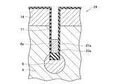
(第1実施例)
図1に、第1実施例である縦型のパワーMOS(請求項でいう半導体装置)100の断面図と、パワーMOS100における電界強度プロファイルを表すグラフを示す。
パワーMOS100は、半導体基板24の表面に配置されているソース電極(請求項でいう表面電極)18と、半導体基板24の裏面に配置されているドレイン電極(請求項でいう裏面電極)26を備えている。半導体基板24内には、ソース領域20と、ボディ領域14と、ボディコンタクト領域16と、ドリフト領域4と、ドレイン領域2が配置されている。ソース領域20は、第1導電型(n型)であり、半導体基板24の表面側に配置されており、ソース電極18に導通している。ドリフト領域4は、第1導電型(n型)であり、半導体基板24の内部に配置されており、第1導電型(n型)のドレイン領域2を介して、ドレイン電極26に導通している。ボディ領域14は、第2導電型(p型)であり、ソース領域20とドリフト領域4を分離している。ボディコンタクト領域16は、第2導電型(p型)の不純物を高濃度に含有し、ボディ領域14の電位をソース電極18の電位によって安定させる。ドレイン領域2は、第1導電型(n型)の不純物を高濃度に含有し、ドレイン電極26との接触抵抗を低下させる。半導体基板24内には、半導体基板24の表面からソース領域20とボディ領域14を貫通してドリフト領域4に達するまで伸びているトレンチ11が配置されている。トレンチ11内にはゲート電極12と浮遊電極8が配置されている。ゲート電極12の壁面は絶縁膜22で被覆されている。ゲート電極12の底面12aは、ボディ領域14の底面14aより深い位置に位置している。浮遊電極8はトレンチ11内のゲート電極12より深い位置に配置されており、壁面を絶縁膜22で被覆されている。浮遊電極8は、トレンチ11内に浮遊しており、絶縁膜22によってトレンチ10外の部材から絶縁されている。耐圧性能を向上させるために、トレンチ11の底面11aを囲む範囲に、第2導電型(p型)の不純物含有領域6が形成されている。不純物含有領域6は、ドリフト領域4内に形成されている。正確には、不純物含有領域6の中心D2の深さは、ドリフト領域4の中間深さD3より深い位置となっている。また、不純物含有領域6の上端は、ドリフト領域4の中間深さD3よりも深い位置となっている。
(First embodiment)
FIG. 1 shows a cross-sectional view of a vertical power MOS (claimed semiconductor device) 100 according to the first embodiment, and a graph showing an electric field intensity profile in the
The
パワーMOS100では、ゲート電極12に電圧を印加することによって、ボディ領域14内にチャネルを形成することができる。ボディ領域14内にチャネルが形成されることによって、ソース領域20とドレイン領域2の間の導通を制御することができる。
In the
次に、図1(a)のパワーMOS100の電界強度プロファイルを表すグラフを,図1(b)を参照して説明する。図1(b)のグラフは、図1(a)のX−X線分に沿った電界強度プロファイルを示している。グラフの横軸は電界強度(V/cm)を示す。グラフの縦軸は半導体基板24の深さ(μm)を示しており、図1(a)のパワーMOS100の断面図で示す深さと対応している。図示Ecは、臨界電界強度を示す。パワーMOS100の耐圧の大きさは、図1(b)のハッチに示す面積に比例する。パワーMOS100は、ゲート電極12の底面12aに対応する深さに、第1の電界強度ピークP1を有している。また、不純物含有領域6の下部近傍に対応する深さD1に、第2の電界強度ピークP2を有している。第1ピークP1における電界強度と、第2ピークP2における電界強度は、いずれも、臨界電界強度Ecに等しい。また、浮遊電極8が配置された深さにおいても、高い電界強度E1を保持している。パワーMOS100では、ゲート電極12の下方に浮遊電極8を配置することで、2つのピークP1,P2が離れていても、2つのピークP1,P2の間に形成される谷の深さを浅くすることができる。これによって、電界強度プロファイルを、図28(b)に示す曲線Lに近づけることができる。図1(b)においてハッチで示す面積が大きくなるため、パワーMOS100の耐圧は高い。
Next, a graph representing the electric field intensity profile of the
パワーMOS100では、浮遊電極8の位置を調整することによって、パワーMOS100をオフしたときにゲート電極12の底面12aの近傍から不純物含有領域6に向けて形成される空乏層の伸びを調整することができる。電界強度プロファイルの形状を調整することで、より高い耐圧性能を得ることができる。また、ゲート電極12をトレンチ11内の深い位置まで配置していないため、ゲート容量を低減することができ、スイッチング損失を低減することもできる。さらに、要求耐圧が低い場合には、ドリフト領域4の不純物濃度を高くすることによってオン抵抗を低減することができるため、オン抵抗が小さい低耐圧型のパワーMOSを実現することもできる。
また、ボディ領域14と不純物含有領域6の間の距離を十分に離すことができるので、ゲート電極12に沿ってボディ領域14を通過してきたキャリアが、不純物含有領域6を迂回しながらドレイン電極26に流れるための有効通過領域を広く確保することができる。このため、低オン抵抗を実現することができる。パワーMOS100では、耐圧とオン抵抗の両者を理論限界値とほぼ同等のレベルにまで向上することができる。
In the
In addition, since the distance between the
図2に、トレンチゲート型のパワーMOSにおける、耐圧とオン抵抗のトレードオフの関係を示す。図2の縦軸は、オン抵抗(mΩ・mm2)を示している。図2の横軸は、耐圧(V)を示す。図2中の曲線は、耐圧とオン抵抗の理論限界を表した理論カーブを示す。従来構造A、従来構造Bは、図29で説明したものと同様であるため説明を省略する。本実施例は、パワーMOS100の測定結果を示している。
パワーMOS100は、図2に示すように、43Vの要求耐圧において、従来のパワーMOSに比して、理論カーブとほぼ一致するほどの耐圧とオン抵抗を実現している。なお、パワーMOS100では、43Vより大きな要求耐圧においても、同様に、理論カーブとほぼ一致するほどの耐圧とオン抵抗を実現できるものと予測される。
FIG. 2 shows a trade-off relationship between breakdown voltage and on-resistance in a trench gate type power MOS. The vertical axis in FIG. 2 indicates the on-resistance (mΩ · mm 2 ). The horizontal axis in FIG. 2 indicates the breakdown voltage (V). The curve in FIG. 2 shows the theoretical curve showing the theoretical limit of withstand voltage and on-resistance. Conventional structure A and conventional structure B are the same as those described with reference to FIG. This example shows the measurement result of the
As shown in FIG. 2, the
図3〜図11に、パワーMOS100を製造する方法を示す。
まず、図3に示すように、n−型のシリコンを材料とする半導体基板24を準備する。次に、半導体基板24内にボロンなどのp型の不純物を注入して熱拡散させることによって、半導体基板24の表面側にボディ領域14を形成する。半導体基板24内のp型不純物が拡散していない領域はn−型のドリフト領域4となる。次に、トレンチ11を形成する位置が開口しているパターンに転写したマスク(図示しない)を用いて、半導体基板24の表面からボディ領域14を貫通してドリフト領域4まで達するトレンチ11を形成する。マスクの材料としては、例えば酸化シリコンを用いることができる。トレンチ11を形成する方法としては、例えばケミカルドライエッチング法を用いることができる。これによって、半導体基板24内に側壁が平滑化されたトレンチ11を形成することができる。トレンチ11の深さは、例えば、半導体基板24の表面から3.0〜3.3μmの深さにすることができる。トレンチ11の幅は、例えば0.4〜0.5μmとすることができる。トレンチ11のテーパ角は、例えば86.0°〜89.0°とすることができる。次に、半導体基板24の表面に熱酸化膜(図示しない)を形成する。次に、この熱酸化膜をマスクとしてトレンチ11の底部11aにp型の不純物を注入して熱拡散させることによって、トレンチ11の底面11aを囲む範囲に不純物含有領域6を形成する。次に、半導体基板24の表面上のマスクと熱酸化膜を除去する。これによって、半導体基板24の表面に清浄なシリコン面が露出する。マスクと熱酸化膜を除去する方法としては、例えばウェットエッチング法などの等方性エッチングを用いることができる。
3 to 11 show a method for manufacturing the
First, as shown in FIG. 3, a
次に、図4に示すように、半導体基板24の表面とトレンチ11の壁面に第1の熱酸化膜21aを形成する。第1の熱酸化膜21aを形成する条件としては、例えば加熱温度を800℃〜1100℃、ガスの種類をO2又はH2/O2又はN2で希釈したH2/O2とすることができる。第1の熱酸化膜21aの厚みは、例えば20nmとすることができる。
Next, as shown in FIG. 4, a first
次に、図5に示すように、第1の熱酸化膜21aの表面に第1のシリコン酸化膜23aを形成する。第1のシリコン酸化膜23aを形成する方法として、例えばCVD(Chemical Vapor Deposition)法を用いることができる。CVD法を用いる場合、製造後の浮遊電極8の底面8aの位置に応じて、第1のシリコン酸化膜23aの堆積量を調整する。第1のシリコン酸化膜23aの種類としては、例えばLP−SiH4−SiO2又はLP−TEOS−SiO2又はAP−O3TEOS−SiO2を用いることができる。第1のシリコン酸化膜23aの厚みは、例えば55nm〜65nmとすることができる。
Next, as shown in FIG. 5, a first
次に、図6に示すように、トレンチ11の内部に第1のポリシリコン8aを充填する。このとき、トレンチ11が第1のポリシリコン8aによって完全に埋め込まれるまで充填する。第1のポリシリコン8aは、製造後のパワーMOS100における浮遊電極8に相当する。第1のポリシリコン8の種類として、例えばSiH4を用いることができる。第1のポリシリコン8aを充填する際の加熱条件は、例えば600℃とすることができる。
Next, as shown in FIG. 6, the inside of the
次に、図7に示すように、第1のポリシリコン8aの一部をエッチングして除去する(エッチバックする)。このとき、製造後の浮遊電極8の上面の位置に応じて、エッチバック量を調整する。エッチングする深さは、例えば、半導体基板の表面から2.5〜2.7μmの深さにすることができる。
Next, as shown in FIG. 7, a part of the
次に、図8に示すように、図7の工程でエッチングした深さと同じ深さまで、第1の熱酸化膜21aの一部および第1のシリコン酸化膜23aの一部をエッチングして除去する。エッチング方法としては、例えばウェットエッチング法又はドライエッチング法を用いることができる。
Next, as shown in FIG. 8, a part of the first
次に、図9に示すように、半導体基板24の表面と露出しているトレンチ11の壁面に第2の熱酸化膜21bを形成する。次に、第2の熱酸化膜21bの表面とポリシリコン8の表面に第2のシリコン酸化膜23bを形成する。第2の熱酸化膜21bおよび第2のシリコン酸化膜23bを形成する条件は、図4、図5の工程で説明した条件と同様である。なお、第2のシリコン酸化膜23bをCVD法によって形成する場合、製造後にゲート電極12の底面となる位置に応じて、第2のシリコン酸化膜23bの堆積量を調整する。
Next, as shown in FIG. 9, a second
次に、図10に示すように、トレンチ11の内部に第2のポリシリコン12aを充填する。このとき、トレンチ11が第2のポリシリコン12aによって完全に埋め込まれるまで充填する。第2のポリシリコン12aは、製造後のパワーMOS100におけるゲート電極12に相当する。第2のポリシリコン12aの種類および加熱条件は図6の工程で説明した条件と同様である。
Next, as shown in FIG. 10, the inside of the
次に、図11に示すように、第2のポリシリコン12aの一部をエッチングして除去する(エッチバックする)。このとき、第2のポリシリコン12aの上面が半導体基板24の表面の高さにほぼ一致するように、エッチバック量を調整する。次に、図1に示すように、半導体基板24の表面から不純物を注入して熱拡散させることによって、半導体基板24の表面側にソース領域20およびボディコンタクト領域16を形成した後、半導体基板24の表面にソース電極18を形成する。次に、半導体基板24の裏面から不純物を注入して熱拡散させることによって、半導体基板24の裏面側にドレイン領域2を形成した後、半導体基板24の裏面にドレイン電極26を形成する。以上の工程によって、パワーMOS100が完成する。なお、図11に示す第1の熱酸化膜21a、第2の熱酸化膜21b、第1のシリコン酸化膜23aおよび第2のシリコン酸化膜23bは全て、図1に示す絶縁膜22に相当する。
Next, as shown in FIG. 11, a part of the
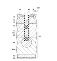
(第2実施例)
図12に、第2実施例であるパワーMOS200の断面図を示す。なお、図12において、図1の参照符号に数字30を加えた部材は、図1で説明した部材と同一であるため、その重複説明を省略する。パワーMOS200では、浮遊電極38の側壁を被覆している絶縁膜52bの厚みW1がゲート電極42の側壁を被覆している絶縁膜52aの厚みW2より厚い。
(Second embodiment)
FIG. 12 shows a cross-sectional view of a
パワーMOS200では、浮遊電極38の側壁を被覆している絶縁膜52aを厚くすることで、オフ時に浮遊電極38の側方のドリフト領域34に発生する電界の強度を緩和している。一方で、浮遊電極38の側壁を被覆している絶縁膜52aの厚みを厚くし過ぎると、浮遊電極38の側壁を被覆している絶縁膜52aに電界が集中し、臨界電界強度Ecを越えて、低い耐圧でブレークダウンが生じる場合がある。パワーMOS200では、浮遊電極38の側壁を被覆している絶縁膜52aの厚みを調整することによって、ブレークダウンを抑制しながら、電界強度プロファイルの形状を、2つのピークのバランスを保ちながら図28(b)に示す曲線Lに近づけている。これによって、パワーMOS200の耐圧をさらに高めることができる。
In the
図13、図14にパワーMOS200を製造する方法を示す。
なお、第1の熱酸化膜の一部および第1のシリコン酸化膜の一部をエッチングして除去するまでの製造過程(第1実施例の図3〜図8の工程に相当)は第1実施例の製造方法と同様であるため、説明を省略する。図13は、第1の熱酸化膜51aの一部および第1のシリコン酸化膜53aの一部をエッチングして除去した後の状態を示す。図示38aは、第1のポリシリコンであり、製造後の浮遊電極38に相当する。本実施例では、第1のシリコン酸化膜53aを形成する工程(第1実施例の図5の工程に相当)において、第1のシリコン酸化膜53aを厚く形成する(例えば130nm)。
FIG. 13 and FIG. 14 show a method for manufacturing the
The manufacturing process (corresponding to the steps of FIGS. 3 to 8 of the first embodiment) until part of the first thermal oxide film and part of the first silicon oxide film are removed by etching is the first. Since it is the same as the manufacturing method of an Example, description is abbreviate | omitted. FIG. 13 shows a state after a part of the first
本実施例の製造方法では、第1の熱酸化膜51aの一部および第1のシリコン酸化膜53aの一部をエッチングして除去した後に、図14に示すように、半導体基板54の表面と露出しているトレンチ11の壁面に第2の熱酸化膜51bを形成する。次に、第2の熱酸化膜51bの表面とポリシリコン38の表面に第2のシリコン酸化膜53bを形成する。このとき、トレンチ41の側壁に堆積させる第2のシリコン酸化膜53bの厚みW3が、トレンチ41の側壁に堆積している第1のシリコン酸化膜53aの厚みW4よりも小さくなるように、第2のシリコン酸化膜53bを形成する(例えば80nm)。第2の熱酸化膜51bおよび第2のシリコン酸化膜53bを形成する条件は、第1実施例の図4、図5の工程で説明した条件と同様である。なお、第2のシリコン酸化膜53bをCVD法によって形成する場合、製造後のゲート電極42の底面の位置に応じて、第2のシリコン酸化膜53bの堆積量を調整する。以降、第1実施例の図10、図11の工程と同様の手順によって、パワーMOS200が完成する。
In the manufacturing method of the present embodiment, after removing a part of the first
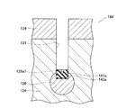
(第3実施例)
図15に、第3実施例であるパワーMOS300の断面図を示す。なお、図15において、図1の参照符号に数字60を加えた部材は、図1で説明した部材と同一であるため、その重複説明を省略する。パワーMOS300では、ドリフト領域64a、64bが、不純物濃度が高い第1導電型(n型)の高濃度領域64bと、不純物濃度が高濃度領域64bよりも低い第1導電型(n型)の低濃度領域64aを備えている。高濃度領域64bはボディ領域74に深い位置で隣接している。低濃度領域64aは高濃度領域64bに深い位置で隣接している。高濃度領域64bの底面は、浮遊電極68の低面とほぼ一致している。
(Third embodiment)
FIG. 15 is a sectional view of a
パワーMOS300では、オンしたときに、高濃度領域64b内に形成されるキャリアの通過領域ではキャリアが流れやすい。このため、トレンチ71に沿ってボディ領域74を通過してきたキャリアを、速やかにドレイン電極86に供給することができ、パワーMOS300のオン抵抗をさらに低減することができる。また、高濃度領域64bでは空乏層が伸び難くなるが、高濃度領域64bが配置される深さには浮遊電極68が配置されている。これによって、空乏層が伸び難くなることが抑制され、十分な耐圧を確保している。
In the
パワーMOS300を製造する方法では、半導体基板84内にボディ領域74を形成する工程の前に、半導体基板84内に高濃度領域64bを形成する。高濃度領域64aを形成する方法としては、2つの方法を用いることができる。第1の方法を図16に示す。第2の方法を図17に示す。図16に示す方法では、半導体基板84の表面にリンなどのn型不純物81を高濃度でイオン注入して熱拡散させる。これによって、半導体基板84の表面側に数μmの厚みの高濃度領域64bを形成する。半導体基板84内のn型不純物81が熱拡散していない領域は、低濃度領域64aとなる。イオン注入の条件として、例えばリンの粒子密度を2×10¹³(cm−3)、イオン注入する際の加速電圧を60keVとすることができる。次に、半導体基板84の表面にp型の不純物を注入して加熱することによって、高濃度領域64bの表面側にボディ領域74を形成する。以降、第1実施例の図3〜図11の工程と同様の手順によってパワーMOS300が完成する。
In the method for manufacturing the
図17に示す方法では、ドレイン領域62となる基板の表面に、n−型の低濃度領域64aとなる第1の半導体領域85をエピタキシャル成長によって形成する。次に、第1の半導体領域85の表面85aに、n+型の高濃度領域64bとなる第2の半導体基板87をエピタキシャル成長によって堆積させる。第1の半導体領域85をエピタキシャル成長させる際に用いる基板の条件として、ヒ素が注入されており、抵抗が0.3Ωの基板を用いることができる。第2の半導体領域87をエピタキシャル成長させる際に用いる基板の条件として、ヒ素が注入されており、抵抗が0.18Ωの基板を用いることができる。次に、第2の半導体領域87の表面にp型の不純物を注入して加熱することによって、高濃度領域64bの表面側にボディ領域74を形成する。以降、第1実施例の図3〜図11の工程と同様の手順によってパワーMOS300が完成する。
In the method shown in FIG. 17, the first semiconductor region 85 to be the n − -type
パワーMOS300では、ドリフト領域64a、64bが、不純物濃度が異なる複数の領域を深さ方向に沿って備えており、各々の領域の不純物濃度が深さ方向に沿って低くなっていることが好ましい。この場合、パワーMOS300のオン時に形成されるキャリアの通過領域において、キャリア抵抗を段階的に低減することができる。各々の領域の厚みと不純物濃度を調整することによって、パワーMOS300のオン時にドリフト領域64a、64b内を通過するキャリアの流れやすさを調整することができる。一例として、ドリフト領域を4つの領域に分割することができる。この場合、深さ方向に沿って深い位置から順に、第1の領域の厚みを3.7μm、不純物濃度を4.0×10¹⁶(cm−3)とすることができる。第2の領域の厚みを0.5μm、不純物濃度を5.0×10¹⁶(cm−3)とすることができる。第3の領域の厚みを0.5μm、不純物濃度を6.0×10¹⁶(cm−3)とすることができる。第4の領域の厚みを1.8μm、不純物濃度を7.0×10¹⁶(cm−3)とすることができる。
In
(第4実施例)
図18に、第4実施例であるパワーMOS400の断面図を示す。なお、図18において、図1の参照符号に数字90を加えた部材は、図1で説明した部材と同一であるため、その重複説明を省略する。パワーMOS400では、ゲート電極102の壁面を被覆している絶縁膜112bの誘電率が浮遊電極98の壁面を被覆している絶縁膜112aの誘電率より高い。
(Fourth embodiment)
FIG. 18 is a sectional view of a
パワーMOS400では、第1〜第3実施例のパワーMOSに比して、オンしたときにゲート電極102の側方にチャネルが形成されやすい。これによって、パワーMOS400のオン抵抗をさらに低減することができる。また、パワーMOS400のオフ時に浮遊電極98が配置されている深さにおいてキャリアが逆方向に流れにくくなる。このため、ブレークダウン電圧が低下することを抑制することができる。
In the
パワーMOS400を製造する方法は、第1実施例のパワーMOS100を製造する方法と同様であり、絶縁膜112a、112bを形成するときの材料のみ異なる。パワーMOS400の製造方法では、第1実施例の図5の工程で、第1のシリコン酸化膜23aの替わりに誘電率の高い高誘電体膜を堆積させる。高誘電体膜の材料としては、例えばTEOSを用いることができる。高誘電体膜の比誘電率は、約3.9であることが好ましい。また、第1実施例の図9の工程で、第2のシリコン酸化膜23bの替わりに誘電率の低い低誘電体膜を堆積させる。低誘電体膜の材料としては、例えば酸化ハフニウムを用いることができる。低誘電体膜の比誘電率は、10〜14であることが好ましい。
The method for manufacturing the
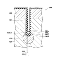
(第5実施例)
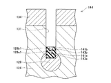
図19に、第5実施例であるパワーMOS500の断面図を示す。なお、図19において、図1の参照符号に数字120を加えた部材は、図1で説明した部材と同一であるため、その重複説明を省略する。パワーMOS500では、ドレイン領域122の不純物濃度が1×1019(cm−3)である。ドリフト領域124の不純物濃度は5×1016(cm−3)である。ボディ領域134の不純物濃度は2×1017(cm−3)である。ボディコンタクト領域136の不純物濃度は1×1019(cm−3)である。パワーMOS500では、4つの浮遊電極128a〜128dがトレンチ131の深さ方向に沿って間隔を空けて配置されている。各浮遊電極128a〜128dの厚みは0.2μmである。また、浮遊電極128a〜128dの各々の間隔がトレンチ131の深さ方向に沿って等比級数的に減少している。すなわち、浮遊電極128cと浮遊電極128dの間隔D4は0.2μmである。浮遊電極128bと浮遊電極128cの間隔D5は0.1μmである。浮遊電極128aと浮遊電極128bの間隔D6は0.05μmである。従って、D5=0.5×D4、D6=0.5×D5の関係が成立する。また、浮遊電極128a〜128dの側壁を被覆している各々の絶縁膜142の厚みがトレンチ131の深さ方向に沿って厚くなっている。パワーMOS500では、浮遊電極128dを被覆している絶縁膜142の厚みを厚みW8とし、浮遊電極128cを被覆している絶縁膜142の厚みを厚みW7とし、浮遊電極128bを被覆している絶縁膜142の厚みを厚みW6とし、浮遊電極128aを被覆している絶縁膜142の厚みを厚みW5とすると、W8<W7<W6<W5が成立する。
(5th Example)
FIG. 19 is a sectional view of a
パワーMOS500では、トレンチ131内における浮遊電極128a〜128dの配置および複数の浮遊電極128a〜128dを被覆している各々の絶縁膜142の厚みを調整することによって、電界強度プロファイルの形状をトレンチ131の深さ方向に沿って調整することができる。隣接する浮遊電極128a〜128dの各々の間隔は等比級数的に減少しているので、電界強度プロファイルの形状を効果的に調整することができる。電界強度プロファイルの形状を図28(b)に示す曲線Lに近づけることによって、パワーMOS500の耐圧をさらに高めることができる。
In the
図20〜図27にパワーMOS500を製造する方法を示す。
なお、第1の熱酸化膜の一部および第1のシリコン酸化膜の一部をエッチングして除去するまでの製造過程(第1実施例の図3〜図8の工程に相当)は第1実施例の製造方法と同様であるため、説明を省略する。図20は、第1の熱酸化膜141aの一部および第1のシリコン酸化膜143aの一部をエッチングして除去した後の状態を示す。エッチングする深さは、例えば2.65μmとすることができる。図示128aは、第1のポリシリコンであり、製造後の浮遊電極128aに相当する。本実施例の製造方法では、第1のシリコン酸化膜143aを形成する工程(第1実施例の図5の工程に相当)において、第1のシリコン酸化膜143aの側壁の幅を厚く形成する(例えば200nm)。
20 to 27 show a method for manufacturing the
The manufacturing process (corresponding to the steps of FIGS. 3 to 8 of the first embodiment) until part of the first thermal oxide film and part of the first silicon oxide film are removed by etching is the first. Since it is the same as the manufacturing method of an Example, description is abbreviate | omitted. FIG. 20 shows a state after part of the first
第1の熱酸化膜141aの一部および第1のシリコン酸化膜143aの一部をエッチングして除去した後に、図21に示すように、半導体基板144の表面と露出しているトレンチ131の壁面に第2の熱酸化膜141bを形成する。次に、第2の熱酸化膜141bの表面と第1のポリシリコン128a1の表面に第2のシリコン酸化膜143bを形成する。このとき、第1のポリシリコン128a1と後述する第2のポリシリコン128b1の間隔が0.05μmとなるように、第2のシリコン酸化膜143bを形成する。さらに、トレンチ131の側壁に堆積させる第2のシリコン酸化膜143bの厚みW10が、第1のポリシリコン128a1の側壁に堆積している第1のシリコン酸化膜143aの厚みW9より小さくなるように、第2のシリコン酸化膜143bを形成する(例えば150nm)。
After etching and removing a part of the first
次に、図22に示すように、トレンチ131の内部に第2のポリシリコン128b1を充填する。このとき、トレンチ131が第2のポリシリコン128b1によって完全に埋め込まれるまで充填する。第2のポリシリコン128b1は、製造後の浮遊電極128bに相当する。
Next, as shown in FIG. 22, the inside of the
次に、図23に示すように、第2のポリシリコン128b1の一部をエッチングして除去する(エッチバックする)。このとき、製造後の浮遊電極128bの上面の位置に応じて、エッチバック量を調整する。エッチングする深さは、例えば2.4μmとすることができる。次に、第2のポリシリコン128b1をエッチングした深さと同じ深さまで、第2の熱酸化膜141bの一部および第2のシリコン酸化膜143bの一部をエッチングして除去する。
Next, as shown in FIG. 23, a part of the second polysilicon 128b1 is removed by etching (etching back). At this time, the etch back amount is adjusted according to the position of the upper surface of the floating
次に、図24に示すように、半導体基板144の表面とトレンチ131の壁面に第3の熱酸化膜141cを形成する。次に、第3の熱酸化膜141cの表面と第2のポリシリコン128b1の表面に第3のシリコン酸化膜143cを形成する。このとき、第2のポリシリコン128b1と後述する第3のポリシリコン128c1の間隔が0.1μmとなるように、第3のシリコン酸化膜143cを形成する。さらに、トレンチ131の側壁に堆積させる第3のシリコン酸化膜143cの厚みW11が、第2のポリシリコン128b1の側壁に堆積している第2のシリコン酸化膜143bの厚みW10より小さくなるように、第3のシリコン酸化膜143cを形成する(例えば100nm)。
Next, as shown in FIG. 24, a third
次に、図25に示すように、トレンチ131の内部に第3のポリシリコン128c1を充填した後に、図22、図23の工程と同様の手順によって、第3のポリシリコン128c1の一部、第3の熱酸化膜141cの一部、第3のシリコン酸化膜143cの一部をエッチングして除去する。このとき、製造後の浮遊電極128cの上面の位置に応じて、第3のポリシリコン128c1のエッチバック量を調整する。エッチングする深さは、例えば2.1μmとすることができる。第3のポリシリコン128c1は、製造後の浮遊電極128cに相当する。
Next, as shown in FIG. 25, after filling the inside of the
次に、図26に示すように、半導体基板144の表面とトレンチ131の壁面に第4の熱酸化膜141dを形成する。次に、第4の熱酸化膜141dの表面と第3のポリシリコン128c1の表面に第4のシリコン酸化膜143dを形成する。このとき、第3のポリシリコン128c1と後述する第4のポリシリコン128d1の間隔が0.2μmとなるように、第4のシリコン酸化膜143dを形成する。さらに、トレンチ131の側壁に堆積される第4のシリコン酸化膜143dの厚みW12が、第3のポリシリコン128c1の側壁に堆積している第3のシリコン酸化膜143cの厚みW11より小さくなるように、第4のシリコン酸化膜143dを形成する(例えば50nm)。
Next, as shown in FIG. 26, a fourth
次に、図27に示すように、トレンチ131の内部に第4のポリシリコン128d1を充填した後に、図22、図23の工程と同様の手順によって、第4のポリシリコン128d1の一部、第4の熱酸化膜141cの一部、第4のシリコン酸化膜143dの一部をエッチングして除去する。このとき、製造後の浮遊電極128dの上面の位置に応じて、エッチバック量を調整する。エッチングする深さは、例えば1.7μmとすることができる。第4のポリシリコン128d1は、製造後の浮遊電極128dに相当する。以降、第1実施例の図9〜図11の工程と同様の手順によって、パワーMOS500が完成する。
Next, as shown in FIG. 27, after filling the inside of the
第1〜第5実施例の製造方法では、シリコン酸化膜の種類としてLP−TEOSを用いることが好ましい。LP−TEOSはガバレッジ性が良好であるため、CVD法によってシリコン酸化膜を堆積させる際に、シリコン酸化膜の厚みを効果的に制御することができる。 In the manufacturing methods of the first to fifth embodiments, LP-TEOS is preferably used as the type of silicon oxide film. Since LP-TEOS has good coverage, the thickness of the silicon oxide film can be effectively controlled when the silicon oxide film is deposited by the CVD method.
第1〜第5実施例の製造方法では、ゲート電極および浮遊電極の材料としてポリシリコンを用いることが好ましい。ポリシリコンの替わりにアルミニウムなどの金属を用いた場合、電極金属を汚染などから保護するための保護膜を形成することが必要となるためである。 In the manufacturing methods of the first to fifth embodiments, it is preferable to use polysilicon as a material for the gate electrode and the floating electrode. This is because when a metal such as aluminum is used instead of polysilicon, it is necessary to form a protective film for protecting the electrode metal from contamination.
第1〜第5実施例の製造方法では、ドリフト領域の濃度および要求耐圧に応じて、ゲート電極と浮遊電極の間の間隔を調整することが好ましい。ドリフト領域の濃度および要求耐圧によって電界強度プロファイルの形状は変化する。ドリフト領域の濃度および要求耐圧に応じて、ゲート電極と浮遊電極の間の間隔を調整することで、電界強度プロファイルの形状を、図28(b)に示す曲線Lに近づけることができ、耐圧を効果的に高めることができる。 In the manufacturing methods of the first to fifth embodiments, it is preferable to adjust the distance between the gate electrode and the floating electrode according to the concentration of the drift region and the required breakdown voltage. The shape of the electric field strength profile changes depending on the concentration of the drift region and the required breakdown voltage. By adjusting the distance between the gate electrode and the floating electrode in accordance with the concentration of the drift region and the required breakdown voltage, the shape of the electric field strength profile can be brought close to the curve L shown in FIG. Can be effectively increased.
第1〜第5実施例のパワーMOSでは、不純物含有領域の上端がドリフト領域の中間深さより浅い位置に形成されていることが好ましい。不純物含有領域の位置が深すぎると、ドリフト領域内を通過するキャリアの抵抗が増大し、オン抵抗が上昇する。このため、不純物含有領域の位置は深すぎないことが好ましい。 In the power MOSs of the first to fifth embodiments, it is preferable that the upper end of the impurity-containing region is formed at a position shallower than the intermediate depth of the drift region. If the position of the impurity-containing region is too deep, the resistance of carriers passing through the drift region increases and the on-resistance increases. For this reason, it is preferable that the position of the impurity-containing region is not too deep.
第1〜第5実施例では、n型を第1導電型とし、p型を第2導電型とする半導体装置を記載したが、n型を第2導電型とし、p型を第1導電型としてもよい。この場合であっても、高い耐圧と低いオン抵抗を兼ね備えたパワーMOSを製造することができる。 In the first to fifth embodiments, the semiconductor device in which the n-type is the first conductivity type and the p-type is the second conductivity type is described. However, the n-type is the second conductivity type and the p-type is the first conductivity type. It is good. Even in this case, a power MOS having both a high breakdown voltage and a low on-resistance can be manufactured.
第1〜第5実施例では、パワーMOSを記載したが、例えばIGBT(Insulated Gate Bipolar Transistor)など、他の半導体装置であってもよい。パワーMOS以外の半導体装置であっても、高い耐圧と低いオン抵抗を兼ね備えた半導体装置を実現することができる。 In the first to fifth embodiments, the power MOS is described. However, other semiconductor devices such as an IGBT (Insulated Gate Bipolar Transistor) may be used. Even a semiconductor device other than a power MOS can realize a semiconductor device having both a high breakdown voltage and a low on-resistance.
以上、本発明の実施例について詳細に説明したが、これらは例示に過ぎず、特許請求の範囲を限定するものではない。特許請求の範囲に記載の技術には、以上に例示した具体例を様々に変形、変更したものが含まれる。
本明細書または図面に説明した技術要素は、単独であるいは各種の組合せによって技術的有用性を発揮するものであり、出願時請求項記載の組合せに限定されるものではない。また、本明細書または図面に例示した技術は複数目的を同時に達成し得るものであり、そのうちの一つの目的を達成すること自体で技術的有用性を持つものである。
As mentioned above, although the Example of this invention was described in detail, these are only illustrations and do not limit a claim. The technology described in the claims includes various modifications and changes of the specific examples illustrated above.
The technical elements described in this specification or the drawings exhibit technical usefulness alone or in various combinations, and are not limited to the combinations described in the claims at the time of filing. In addition, the technology exemplified in this specification or the drawings can achieve a plurality of objects at the same time, and has technical usefulness by achieving one of the objects.
2、32、62、92、122、202:ドレイン領域
4、34、94、124、204:ドリフト領域
6、36、66、96、126、206:不純物含有領域
8、38、68、98、128a、128b、128c、128d:浮遊電極
11、41、71、101、131、211:トレンチ
11a、41a、71a、101a、131a、211a:トレンチの底部
12、42、72、102、132、212:ゲート電極
14、44、74、104、134、214:ボディ領域
14a:ボディ領域の底面
16、46、76、106、136、216:ボディコンタクト領域
18、48、78、108、138、218:表面電極
20、50、80、110、140、220:ソース領域
21a、51a、141a:第1の熱酸化膜
21b、51b、141b:第2の熱酸化膜
22、52a、52b、82:絶縁膜
23a、53a、143a:第1のシリコン酸化膜
23b、53b、143b:第2のシリコン酸化膜
24、54、84、114、144、224:半導体基板
26、56、86、116、146、226:裏面電極
64a:低濃度領域(ドリフト領域)
64b:高濃度領域(ドリフト領域)
81:n型不純物
85:第1の半導体領域
85a:第1の半導体領域の表面
87:第2の半導体領域
100、200、300、400、500、600:パワーMOS
128c1:第3のポリシリコン
128d1:第4のポリシリコン
141c:第3の熱酸化膜
141d:第4の熱酸化膜
143c:第3のシリコン酸化膜
143d:第4のシリコン酸化膜
2, 32, 62, 92, 122, 202: Drain regions 4, 34, 94, 124, 204: Drift regions 6, 36, 66, 96, 126, 206: Impurity-containing regions 8, 38, 68, 98, 128a 128b, 128c, 128d: floating electrodes 11, 41, 71, 101, 131, 211: trenches 11a, 41a, 71a, 101a, 131a, 211a: bottoms of trenches 12, 42, 72, 102, 132, 212: gates Electrodes 14, 44, 74, 104, 134, 214: body region 14a: bottom surface 16, 46, 76, 106, 136, 216 of body region: body contact regions 18, 48, 78, 108, 138, 218: surface electrode 20, 50, 80, 110, 140, 220: source regions 21a, 51a, 141a: first thermal oxide film 1b, 51b, 141b: second thermal oxide films 22, 52a, 52b, 82: insulating films 23a, 53a, 143a: first silicon oxide films 23b, 53b, 143b: second silicon oxide films 24, 54, 84, 114, 144, 224: Semiconductor substrate 26, 56, 86, 116, 146, 226: Back electrode 64a: Low concentration region (drift region)
64b: High concentration region (drift region)
81: n-type impurity 85: first semiconductor region 85a: surface of the first semiconductor region 87:
128c1: third polysilicon 128d1:
Claims (5)
前記半導体基板の表面側に配置されている第2導電型のボディ領域と、
前記半導体基板内の前記ボディ領域より深い位置に配置されている第1導電型のドリフト領域と、
前記半導体基板の表面から前記ボディ領域を貫通して前記ドリフト領域に達するまで伸びているトレンチと、
そのトレンチの底面を囲む範囲に配置されている第2導電型の不純物含有領域と、
前記トレンチ内に配置されており、壁面が絶縁膜で被覆されているとともに、前記ボディ領域の底面より深い位置まで伸びているゲート電極と、
前記トレンチ内の前記ゲート電極より深い位置に配置されており、壁面が絶縁膜で被覆されている浮遊電極を備えており、
前記不純物含有領域の中心が、前記ドリフト領域の中間深さより深い位置に配置されており、
前記トレンチ内のゲート電極より深い位置に複数の浮遊電極が深さ方向に間隔を空けて配置されており、各々の浮遊電極の間隔が深さ方向に沿って等比級数的に減少していることを特徴とする半導体装置。 A front surface electrode is disposed on the front surface of the semiconductor substrate, and a back surface electrode is disposed on the back surface of the semiconductor substrate.
A body region of a second conductivity type disposed on the surface side of the semiconductor substrate;
A drift region of a first conductivity type disposed at a position deeper than the body region in the semiconductor substrate;
A trench extending from the surface of the semiconductor substrate to the drift region through the body region;
An impurity-containing region of a second conductivity type disposed in a range surrounding the bottom surface of the trench;
A gate electrode disposed in the trench, having a wall surface covered with an insulating film and extending to a position deeper than a bottom surface of the body region;
It is disposed at a position deeper than the gate electrode in the trench, and includes a floating electrode whose wall surface is covered with an insulating film,
The center of the impurity-containing region is disposed at a position deeper than the intermediate depth of the drift region ,
A plurality of floating electrodes are arranged in the depth direction at a position deeper than the gate electrode in the trench, and the intervals between the floating electrodes are reduced geometrically along the depth direction. A semiconductor device.
Priority Applications (1)
| Application Number | Priority Date | Filing Date | Title |
|---|---|---|---|
| JP2008306551A JP5195357B2 (en) | 2008-12-01 | 2008-12-01 | Semiconductor device |
Applications Claiming Priority (1)
| Application Number | Priority Date | Filing Date | Title |
|---|---|---|---|
| JP2008306551A JP5195357B2 (en) | 2008-12-01 | 2008-12-01 | Semiconductor device |
Publications (2)
| Publication Number | Publication Date |
|---|---|
| JP2010129973A JP2010129973A (en) | 2010-06-10 |
| JP5195357B2 true JP5195357B2 (en) | 2013-05-08 |
Family
ID=42330126
Family Applications (1)
| Application Number | Title | Priority Date | Filing Date |
|---|---|---|---|
| JP2008306551A Active JP5195357B2 (en) | 2008-12-01 | 2008-12-01 | Semiconductor device |
Country Status (1)
| Country | Link |
|---|---|
| JP (1) | JP5195357B2 (en) |
Families Citing this family (24)
| Publication number | Priority date | Publication date | Assignee | Title |
|---|---|---|---|---|
| JP2011159763A (en) * | 2010-01-29 | 2011-08-18 | Toshiba Corp | Power semiconductor device |
| US8461646B2 (en) * | 2011-02-04 | 2013-06-11 | Vishay General Semiconductor Llc | Trench MOS barrier schottky (TMBS) having multiple floating gates |
| JP2013201267A (en) * | 2012-03-23 | 2013-10-03 | Toshiba Corp | Semiconductor device and method of manufacturing the same |
| JP5579216B2 (en) * | 2012-03-26 | 2014-08-27 | 株式会社東芝 | Semiconductor device and manufacturing method thereof |
| US20130307058A1 (en) * | 2012-05-18 | 2013-11-21 | Infineon Technologies Austria Ag | Semiconductor Devices Including Superjunction Structure and Method of Manufacturing |
| KR101388706B1 (en) * | 2012-08-30 | 2014-04-24 | 삼성전기주식회사 | Power semiconductor device and method of manufacturing the same |
| JP5799046B2 (en) | 2013-03-22 | 2015-10-21 | 株式会社東芝 | Semiconductor device |
| JP6078390B2 (en) * | 2013-03-25 | 2017-02-08 | ルネサスエレクトロニクス株式会社 | Semiconductor device |
| KR101934893B1 (en) | 2013-03-27 | 2019-01-03 | 삼성전자 주식회사 | Method of Fabricating a Semiconductor Device Having a Grooved Source Contact Region |
| KR101828495B1 (en) | 2013-03-27 | 2018-02-12 | 삼성전자주식회사 | Semiconductor Devices Having a Planar Source Electrode |
| DE102013213026A1 (en) * | 2013-07-03 | 2015-01-08 | Robert Bosch Gmbh | Field plate trench FET and a semiconductor device |
| JP2016181617A (en) * | 2015-03-24 | 2016-10-13 | 株式会社デンソー | Semiconductor device |
| JP2016181618A (en) * | 2015-03-24 | 2016-10-13 | 株式会社デンソー | Semiconductor device |
| JP6914190B2 (en) * | 2015-04-27 | 2021-08-04 | ローム株式会社 | Semiconductor devices and methods for manufacturing semiconductor devices |
| US9299830B1 (en) * | 2015-05-07 | 2016-03-29 | Texas Instruments Incorporated | Multiple shielding trench gate fet |
| JP6301882B2 (en) * | 2015-08-21 | 2018-03-28 | トヨタ自動車株式会社 | Semiconductor device manufacturing method and semiconductor device |
| CN105957884A (en) * | 2016-06-24 | 2016-09-21 | 上海格瑞宝电子有限公司 | Split-gate gate trench structure and trench schottky diode and preparation method therefor |
| JP2018152460A (en) * | 2017-03-13 | 2018-09-27 | サンケン電気株式会社 | Controller, and system including controller and semiconductor device controlled by that controller |
| JP6825520B2 (en) * | 2017-09-14 | 2021-02-03 | 三菱電機株式会社 | Semiconductor devices, semiconductor device manufacturing methods, power conversion devices |
| CN109887989A (en) * | 2017-12-06 | 2019-06-14 | 深圳尚阳通科技有限公司 | A kind of shield grid power device and manufacturing method |
| CN113690293B (en) * | 2020-05-18 | 2024-04-12 | 华润微电子(重庆)有限公司 | IGBT device and preparation method thereof |
| CN113690301B (en) * | 2020-05-18 | 2024-01-26 | 华润微电子(重庆)有限公司 | Semiconductor device and method for manufacturing the same |
| CN113690302A (en) * | 2020-05-18 | 2021-11-23 | 华润微电子(重庆)有限公司 | Semiconductor device and method for manufacturing the same |
| JP7438080B2 (en) * | 2020-10-30 | 2024-02-26 | 三菱電機株式会社 | semiconductor equipment |
Family Cites Families (5)
| Publication number | Priority date | Publication date | Assignee | Title |
|---|---|---|---|---|
| EP1170803A3 (en) * | 2000-06-08 | 2002-10-09 | Siliconix Incorporated | Trench gate MOSFET and method of making the same |
| JP4528460B2 (en) * | 2000-06-30 | 2010-08-18 | 株式会社東芝 | Semiconductor element |
| JP4202149B2 (en) * | 2003-01-28 | 2008-12-24 | ローム株式会社 | Semiconductor device and manufacturing method thereof |
| CN103199017B (en) * | 2003-12-30 | 2016-08-03 | 飞兆半导体公司 | Form buried conductive layer method, material thickness control methods, form transistor method |
| DE102006036347B4 (en) * | 2006-08-03 | 2012-01-12 | Infineon Technologies Austria Ag | Semiconductor device with a space-saving edge structure |
-
2008
- 2008-12-01 JP JP2008306551A patent/JP5195357B2/en active Active
Also Published As
| Publication number | Publication date |
|---|---|
| JP2010129973A (en) | 2010-06-10 |
Similar Documents
| Publication | Publication Date | Title |
|---|---|---|
| JP5195357B2 (en) | Semiconductor device | |
| TWI509809B (en) | High density trench-based power mosfets with self-aligned active contacts and method for making such devices | |
| WO2017043606A1 (en) | Silicon carbide semiconductor device | |
| TWI412071B (en) | Method of forming a self-aligned charge balanced power dmos | |
| TWI478241B (en) | Mosfet active area and edge termination area charge balance | |
| JP4028482B2 (en) | Power MOSFET having trench gate electrode and manufacturing method thereof | |
| US8080846B2 (en) | Semiconductor device having improved breakdown voltage and method of manufacturing the same | |
| CN106796955B (en) | Semiconductor device with a plurality of semiconductor chips | |
| JP2006128507A (en) | Insulated-gate semiconductor device and manufacturing method thereof | |
| JP2008546216A (en) | Charge balanced field effect transistor | |
| US7494876B1 (en) | Trench-gated MIS device having thick polysilicon insulation layer at trench bottom and method of fabricating the same | |
| KR20100029701A (en) | Semiconductor trench structure having a sealing plug and method | |
| CN108604552B (en) | Semiconductor device and method for manufacturing such a semiconductor device | |
| US11152503B1 (en) | Silicon carbide MOSFET with wave-shaped channel regions | |
| US11245016B2 (en) | Silicon carbide trench semiconductor device | |
| KR101912030B1 (en) | Combined gate and source trench formation and related structure | |
| US8624302B2 (en) | Structure and method for post oxidation silicon trench bottom shaping | |
| EP1162665A2 (en) | Trench gate MIS device and method of fabricating the same | |
| JP4500639B2 (en) | Trench gate type semiconductor device and manufacturing method thereof | |
| TWI803288B (en) | Integrated planar-trench gate power mosfet | |
| TWI557807B (en) | Semiconductor device and related fabrication methods | |
| KR20170080510A (en) | Transistor device with field electrode | |
| JP5747891B2 (en) | Semiconductor device | |
| CN208589449U (en) | A kind of trench-gate device structure with current-carrying subpool | |
| US9991379B1 (en) | Semiconductor device with a gate insulating film formed on an inner wall of a trench, and method of manufacturing the same |
Legal Events
| Date | Code | Title | Description |
|---|---|---|---|
| A621 | Written request for application examination |
Free format text: JAPANESE INTERMEDIATE CODE: A621 Effective date: 20110519 |
|
| A977 | Report on retrieval |
Free format text: JAPANESE INTERMEDIATE CODE: A971007 Effective date: 20121012 |
|
| A131 | Notification of reasons for refusal |
Free format text: JAPANESE INTERMEDIATE CODE: A131 Effective date: 20121030 |
|
| A521 | Written amendment |
Free format text: JAPANESE INTERMEDIATE CODE: A523 Effective date: 20121213 |
|
| TRDD | Decision of grant or rejection written | ||
| A01 | Written decision to grant a patent or to grant a registration (utility model) |
Free format text: JAPANESE INTERMEDIATE CODE: A01 Effective date: 20130108 |
|
| A61 | First payment of annual fees (during grant procedure) |
Free format text: JAPANESE INTERMEDIATE CODE: A61 Effective date: 20130121 |
|
| FPAY | Renewal fee payment (event date is renewal date of database) |
Free format text: PAYMENT UNTIL: 20160215 Year of fee payment: 3 |
|
| R151 | Written notification of patent or utility model registration |
Ref document number: 5195357 Country of ref document: JP Free format text: JAPANESE INTERMEDIATE CODE: R151 |
|
| FPAY | Renewal fee payment (event date is renewal date of database) |
Free format text: PAYMENT UNTIL: 20160215 Year of fee payment: 3 |