JP6825520B2 - Semiconductor devices, semiconductor device manufacturing methods, power conversion devices - Google Patents
Semiconductor devices, semiconductor device manufacturing methods, power conversion devices Download PDFInfo
- Publication number
- JP6825520B2 JP6825520B2 JP2017176838A JP2017176838A JP6825520B2 JP 6825520 B2 JP6825520 B2 JP 6825520B2 JP 2017176838 A JP2017176838 A JP 2017176838A JP 2017176838 A JP2017176838 A JP 2017176838A JP 6825520 B2 JP6825520 B2 JP 6825520B2
- Authority
- JP
- Japan
- Prior art keywords
- layer
- conductive type
- insulating film
- channel
- carrier store
- Prior art date
- Legal status (The legal status is an assumption and is not a legal conclusion. Google has not performed a legal analysis and makes no representation as to the accuracy of the status listed.)
- Active
Links
- 239000004065 semiconductor Substances 0.000 title claims description 145
- 238000004519 manufacturing process Methods 0.000 title claims description 43
- 238000006243 chemical reaction Methods 0.000 title claims description 35
- 239000000758 substrate Substances 0.000 claims description 117
- 238000009792 diffusion process Methods 0.000 claims description 57
- 238000000034 method Methods 0.000 claims description 55
- 239000004020 conductor Substances 0.000 claims description 43
- 238000002955 isolation Methods 0.000 claims description 23
- 238000005530 etching Methods 0.000 claims description 12
- 238000000926 separation method Methods 0.000 claims description 11
- 238000007667 floating Methods 0.000 claims description 10
- 239000012535 impurity Substances 0.000 claims description 8
- 229910021420 polycrystalline silicon Inorganic materials 0.000 claims description 7
- 229920005591 polysilicon Polymers 0.000 claims description 7
- 238000005468 ion implantation Methods 0.000 claims description 5
- 230000001590 oxidative effect Effects 0.000 claims description 3
- 239000010410 layer Substances 0.000 description 323
- 238000006073 displacement reaction Methods 0.000 description 13
- 230000003647 oxidation Effects 0.000 description 11
- 238000007254 oxidation reaction Methods 0.000 description 11
- 230000007257 malfunction Effects 0.000 description 5
- 238000000151 deposition Methods 0.000 description 4
- 230000000694 effects Effects 0.000 description 4
- 238000003860 storage Methods 0.000 description 4
- 230000015572 biosynthetic process Effects 0.000 description 3
- 239000000969 carrier Substances 0.000 description 3
- 150000002500 ions Chemical class 0.000 description 3
- 239000000463 material Substances 0.000 description 3
- 230000008719 thickening Effects 0.000 description 3
- 238000010586 diagram Methods 0.000 description 2
- 239000011229 interlayer Substances 0.000 description 2
- VYPSYNLAJGMNEJ-UHFFFAOYSA-N Silicium dioxide Chemical compound O=[Si]=O VYPSYNLAJGMNEJ-UHFFFAOYSA-N 0.000 description 1
- 238000009825 accumulation Methods 0.000 description 1
- 230000008021 deposition Effects 0.000 description 1
- 238000009826 distribution Methods 0.000 description 1
- 238000005265 energy consumption Methods 0.000 description 1
- 230000009931 harmful effect Effects 0.000 description 1
- 238000010438 heat treatment Methods 0.000 description 1
- 230000006698 induction Effects 0.000 description 1
- 230000010355 oscillation Effects 0.000 description 1
- 238000010248 power generation Methods 0.000 description 1
- 238000011084 recovery Methods 0.000 description 1
- 229910052710 silicon Inorganic materials 0.000 description 1
- 239000010703 silicon Substances 0.000 description 1
- 229910052814 silicon oxide Inorganic materials 0.000 description 1
Images


Classifications
-
- H—ELECTRICITY
- H01—ELECTRIC ELEMENTS
- H01L—SEMICONDUCTOR DEVICES NOT COVERED BY CLASS H10
- H01L29/00—Semiconductor devices adapted for rectifying, amplifying, oscillating or switching, or capacitors or resistors with at least one potential-jump barrier or surface barrier, e.g. PN junction depletion layer or carrier concentration layer; Details of semiconductor bodies or of electrodes thereof ; Multistep manufacturing processes therefor
- H01L29/40—Electrodes ; Multistep manufacturing processes therefor
- H01L29/41—Electrodes ; Multistep manufacturing processes therefor characterised by their shape, relative sizes or dispositions
- H01L29/423—Electrodes ; Multistep manufacturing processes therefor characterised by their shape, relative sizes or dispositions not carrying the current to be rectified, amplified or switched
- H01L29/42312—Gate electrodes for field effect devices
- H01L29/42316—Gate electrodes for field effect devices for field-effect transistors
- H01L29/4232—Gate electrodes for field effect devices for field-effect transistors with insulated gate
- H01L29/42356—Disposition, e.g. buried gate electrode
- H01L29/4236—Disposition, e.g. buried gate electrode within a trench, e.g. trench gate electrode, groove gate electrode
-
- H—ELECTRICITY
- H01—ELECTRIC ELEMENTS
- H01L—SEMICONDUCTOR DEVICES NOT COVERED BY CLASS H10
- H01L29/00—Semiconductor devices adapted for rectifying, amplifying, oscillating or switching, or capacitors or resistors with at least one potential-jump barrier or surface barrier, e.g. PN junction depletion layer or carrier concentration layer; Details of semiconductor bodies or of electrodes thereof ; Multistep manufacturing processes therefor
- H01L29/66—Types of semiconductor device ; Multistep manufacturing processes therefor
- H01L29/68—Types of semiconductor device ; Multistep manufacturing processes therefor controllable by only the electric current supplied, or only the electric potential applied, to an electrode which does not carry the current to be rectified, amplified or switched
- H01L29/70—Bipolar devices
- H01L29/72—Transistor-type devices, i.e. able to continuously respond to applied control signals
- H01L29/739—Transistor-type devices, i.e. able to continuously respond to applied control signals controlled by field-effect, e.g. bipolar static induction transistors [BSIT]
- H01L29/7393—Insulated gate bipolar mode transistors, i.e. IGBT; IGT; COMFET
- H01L29/7395—Vertical transistors, e.g. vertical IGBT
-
- H—ELECTRICITY
- H01—ELECTRIC ELEMENTS
- H01L—SEMICONDUCTOR DEVICES NOT COVERED BY CLASS H10
- H01L29/00—Semiconductor devices adapted for rectifying, amplifying, oscillating or switching, or capacitors or resistors with at least one potential-jump barrier or surface barrier, e.g. PN junction depletion layer or carrier concentration layer; Details of semiconductor bodies or of electrodes thereof ; Multistep manufacturing processes therefor
- H01L29/02—Semiconductor bodies ; Multistep manufacturing processes therefor
- H01L29/06—Semiconductor bodies ; Multistep manufacturing processes therefor characterised by their shape; characterised by the shapes, relative sizes, or dispositions of the semiconductor regions ; characterised by the concentration or distribution of impurities within semiconductor regions
- H01L29/0684—Semiconductor bodies ; Multistep manufacturing processes therefor characterised by their shape; characterised by the shapes, relative sizes, or dispositions of the semiconductor regions ; characterised by the concentration or distribution of impurities within semiconductor regions characterised by the shape, relative sizes or dispositions of the semiconductor regions or junctions between the regions
- H01L29/0692—Surface layout
- H01L29/0696—Surface layout of cellular field-effect devices, e.g. multicellular DMOS transistors or IGBTs
-
- H—ELECTRICITY
- H01—ELECTRIC ELEMENTS
- H01L—SEMICONDUCTOR DEVICES NOT COVERED BY CLASS H10
- H01L29/00—Semiconductor devices adapted for rectifying, amplifying, oscillating or switching, or capacitors or resistors with at least one potential-jump barrier or surface barrier, e.g. PN junction depletion layer or carrier concentration layer; Details of semiconductor bodies or of electrodes thereof ; Multistep manufacturing processes therefor
- H01L29/02—Semiconductor bodies ; Multistep manufacturing processes therefor
- H01L29/06—Semiconductor bodies ; Multistep manufacturing processes therefor characterised by their shape; characterised by the shapes, relative sizes, or dispositions of the semiconductor regions ; characterised by the concentration or distribution of impurities within semiconductor regions
- H01L29/08—Semiconductor bodies ; Multistep manufacturing processes therefor characterised by their shape; characterised by the shapes, relative sizes, or dispositions of the semiconductor regions ; characterised by the concentration or distribution of impurities within semiconductor regions with semiconductor regions connected to an electrode carrying current to be rectified, amplified or switched and such electrode being part of a semiconductor device which comprises three or more electrodes
- H01L29/0843—Source or drain regions of field-effect devices
- H01L29/0847—Source or drain regions of field-effect devices of field-effect transistors with insulated gate
- H01L29/0852—Source or drain regions of field-effect devices of field-effect transistors with insulated gate of DMOS transistors
- H01L29/0873—Drain regions
- H01L29/0878—Impurity concentration or distribution
-
- H—ELECTRICITY
- H01—ELECTRIC ELEMENTS
- H01L—SEMICONDUCTOR DEVICES NOT COVERED BY CLASS H10
- H01L29/00—Semiconductor devices adapted for rectifying, amplifying, oscillating or switching, or capacitors or resistors with at least one potential-jump barrier or surface barrier, e.g. PN junction depletion layer or carrier concentration layer; Details of semiconductor bodies or of electrodes thereof ; Multistep manufacturing processes therefor
- H01L29/02—Semiconductor bodies ; Multistep manufacturing processes therefor
- H01L29/06—Semiconductor bodies ; Multistep manufacturing processes therefor characterised by their shape; characterised by the shapes, relative sizes, or dispositions of the semiconductor regions ; characterised by the concentration or distribution of impurities within semiconductor regions
- H01L29/10—Semiconductor bodies ; Multistep manufacturing processes therefor characterised by their shape; characterised by the shapes, relative sizes, or dispositions of the semiconductor regions ; characterised by the concentration or distribution of impurities within semiconductor regions with semiconductor regions connected to an electrode not carrying current to be rectified, amplified or switched and such electrode being part of a semiconductor device which comprises three or more electrodes
- H01L29/1095—Body region, i.e. base region, of DMOS transistors or IGBTs
-
- H—ELECTRICITY
- H01—ELECTRIC ELEMENTS
- H01L—SEMICONDUCTOR DEVICES NOT COVERED BY CLASS H10
- H01L29/00—Semiconductor devices adapted for rectifying, amplifying, oscillating or switching, or capacitors or resistors with at least one potential-jump barrier or surface barrier, e.g. PN junction depletion layer or carrier concentration layer; Details of semiconductor bodies or of electrodes thereof ; Multistep manufacturing processes therefor
- H01L29/40—Electrodes ; Multistep manufacturing processes therefor
- H01L29/402—Field plates
- H01L29/407—Recessed field plates, e.g. trench field plates, buried field plates
-
- H—ELECTRICITY
- H01—ELECTRIC ELEMENTS
- H01L—SEMICONDUCTOR DEVICES NOT COVERED BY CLASS H10
- H01L29/00—Semiconductor devices adapted for rectifying, amplifying, oscillating or switching, or capacitors or resistors with at least one potential-jump barrier or surface barrier, e.g. PN junction depletion layer or carrier concentration layer; Details of semiconductor bodies or of electrodes thereof ; Multistep manufacturing processes therefor
- H01L29/40—Electrodes ; Multistep manufacturing processes therefor
- H01L29/41—Electrodes ; Multistep manufacturing processes therefor characterised by their shape, relative sizes or dispositions
- H01L29/423—Electrodes ; Multistep manufacturing processes therefor characterised by their shape, relative sizes or dispositions not carrying the current to be rectified, amplified or switched
- H01L29/42312—Gate electrodes for field effect devices
- H01L29/42316—Gate electrodes for field effect devices for field-effect transistors
- H01L29/4232—Gate electrodes for field effect devices for field-effect transistors with insulated gate
- H01L29/42364—Gate electrodes for field effect devices for field-effect transistors with insulated gate characterised by the insulating layer, e.g. thickness or uniformity
- H01L29/42368—Gate electrodes for field effect devices for field-effect transistors with insulated gate characterised by the insulating layer, e.g. thickness or uniformity the thickness being non-uniform
-
- H—ELECTRICITY
- H01—ELECTRIC ELEMENTS
- H01L—SEMICONDUCTOR DEVICES NOT COVERED BY CLASS H10
- H01L29/00—Semiconductor devices adapted for rectifying, amplifying, oscillating or switching, or capacitors or resistors with at least one potential-jump barrier or surface barrier, e.g. PN junction depletion layer or carrier concentration layer; Details of semiconductor bodies or of electrodes thereof ; Multistep manufacturing processes therefor
- H01L29/40—Electrodes ; Multistep manufacturing processes therefor
- H01L29/41—Electrodes ; Multistep manufacturing processes therefor characterised by their shape, relative sizes or dispositions
- H01L29/423—Electrodes ; Multistep manufacturing processes therefor characterised by their shape, relative sizes or dispositions not carrying the current to be rectified, amplified or switched
- H01L29/42312—Gate electrodes for field effect devices
- H01L29/42316—Gate electrodes for field effect devices for field-effect transistors
- H01L29/4232—Gate electrodes for field effect devices for field-effect transistors with insulated gate
- H01L29/42372—Gate electrodes for field effect devices for field-effect transistors with insulated gate characterised by the conducting layer, e.g. the length, the sectional shape or the lay-out
- H01L29/42376—Gate electrodes for field effect devices for field-effect transistors with insulated gate characterised by the conducting layer, e.g. the length, the sectional shape or the lay-out characterised by the length or the sectional shape
-
- H—ELECTRICITY
- H01—ELECTRIC ELEMENTS
- H01L—SEMICONDUCTOR DEVICES NOT COVERED BY CLASS H10
- H01L29/00—Semiconductor devices adapted for rectifying, amplifying, oscillating or switching, or capacitors or resistors with at least one potential-jump barrier or surface barrier, e.g. PN junction depletion layer or carrier concentration layer; Details of semiconductor bodies or of electrodes thereof ; Multistep manufacturing processes therefor
- H01L29/66—Types of semiconductor device ; Multistep manufacturing processes therefor
- H01L29/68—Types of semiconductor device ; Multistep manufacturing processes therefor controllable by only the electric current supplied, or only the electric potential applied, to an electrode which does not carry the current to be rectified, amplified or switched
- H01L29/70—Bipolar devices
- H01L29/72—Transistor-type devices, i.e. able to continuously respond to applied control signals
- H01L29/739—Transistor-type devices, i.e. able to continuously respond to applied control signals controlled by field-effect, e.g. bipolar static induction transistors [BSIT]
- H01L29/7393—Insulated gate bipolar mode transistors, i.e. IGBT; IGT; COMFET
- H01L29/7394—Insulated gate bipolar mode transistors, i.e. IGBT; IGT; COMFET on an insulating layer or substrate, e.g. thin film device or device isolated from the bulk substrate
-
- H—ELECTRICITY
- H01—ELECTRIC ELEMENTS
- H01L—SEMICONDUCTOR DEVICES NOT COVERED BY CLASS H10
- H01L29/00—Semiconductor devices adapted for rectifying, amplifying, oscillating or switching, or capacitors or resistors with at least one potential-jump barrier or surface barrier, e.g. PN junction depletion layer or carrier concentration layer; Details of semiconductor bodies or of electrodes thereof ; Multistep manufacturing processes therefor
- H01L29/66—Types of semiconductor device ; Multistep manufacturing processes therefor
- H01L29/68—Types of semiconductor device ; Multistep manufacturing processes therefor controllable by only the electric current supplied, or only the electric potential applied, to an electrode which does not carry the current to be rectified, amplified or switched
- H01L29/70—Bipolar devices
- H01L29/72—Transistor-type devices, i.e. able to continuously respond to applied control signals
- H01L29/739—Transistor-type devices, i.e. able to continuously respond to applied control signals controlled by field-effect, e.g. bipolar static induction transistors [BSIT]
- H01L29/7393—Insulated gate bipolar mode transistors, i.e. IGBT; IGT; COMFET
- H01L29/7395—Vertical transistors, e.g. vertical IGBT
- H01L29/7396—Vertical transistors, e.g. vertical IGBT with a non planar surface, e.g. with a non planar gate or with a trench or recess or pillar in the surface of the emitter, base or collector region for improving current density or short circuiting the emitter and base regions
- H01L29/7397—Vertical transistors, e.g. vertical IGBT with a non planar surface, e.g. with a non planar gate or with a trench or recess or pillar in the surface of the emitter, base or collector region for improving current density or short circuiting the emitter and base regions and a gate structure lying on a slanted or vertical surface or formed in a groove, e.g. trench gate IGBT
-
- H—ELECTRICITY
- H01—ELECTRIC ELEMENTS
- H01L—SEMICONDUCTOR DEVICES NOT COVERED BY CLASS H10
- H01L29/00—Semiconductor devices adapted for rectifying, amplifying, oscillating or switching, or capacitors or resistors with at least one potential-jump barrier or surface barrier, e.g. PN junction depletion layer or carrier concentration layer; Details of semiconductor bodies or of electrodes thereof ; Multistep manufacturing processes therefor
- H01L29/66—Types of semiconductor device ; Multistep manufacturing processes therefor
- H01L29/68—Types of semiconductor device ; Multistep manufacturing processes therefor controllable by only the electric current supplied, or only the electric potential applied, to an electrode which does not carry the current to be rectified, amplified or switched
- H01L29/76—Unipolar devices, e.g. field effect transistors
- H01L29/772—Field effect transistors
- H01L29/78—Field effect transistors with field effect produced by an insulated gate
- H01L29/7801—DMOS transistors, i.e. MISFETs with a channel accommodating body or base region adjoining a drain drift region
- H01L29/7802—Vertical DMOS transistors, i.e. VDMOS transistors
- H01L29/7813—Vertical DMOS transistors, i.e. VDMOS transistors with trench gate electrode, e.g. UMOS transistors
-
- H—ELECTRICITY
- H01—ELECTRIC ELEMENTS
- H01L—SEMICONDUCTOR DEVICES NOT COVERED BY CLASS H10
- H01L29/00—Semiconductor devices adapted for rectifying, amplifying, oscillating or switching, or capacitors or resistors with at least one potential-jump barrier or surface barrier, e.g. PN junction depletion layer or carrier concentration layer; Details of semiconductor bodies or of electrodes thereof ; Multistep manufacturing processes therefor
- H01L29/66—Types of semiconductor device ; Multistep manufacturing processes therefor
- H01L29/68—Types of semiconductor device ; Multistep manufacturing processes therefor controllable by only the electric current supplied, or only the electric potential applied, to an electrode which does not carry the current to be rectified, amplified or switched
- H01L29/76—Unipolar devices, e.g. field effect transistors
- H01L29/772—Field effect transistors
- H01L29/78—Field effect transistors with field effect produced by an insulated gate
- H01L29/7827—Vertical transistors
-
- H—ELECTRICITY
- H01—ELECTRIC ELEMENTS
- H01L—SEMICONDUCTOR DEVICES NOT COVERED BY CLASS H10
- H01L29/00—Semiconductor devices adapted for rectifying, amplifying, oscillating or switching, or capacitors or resistors with at least one potential-jump barrier or surface barrier, e.g. PN junction depletion layer or carrier concentration layer; Details of semiconductor bodies or of electrodes thereof ; Multistep manufacturing processes therefor
- H01L29/02—Semiconductor bodies ; Multistep manufacturing processes therefor
- H01L29/06—Semiconductor bodies ; Multistep manufacturing processes therefor characterised by their shape; characterised by the shapes, relative sizes, or dispositions of the semiconductor regions ; characterised by the concentration or distribution of impurities within semiconductor regions
- H01L29/0603—Semiconductor bodies ; Multistep manufacturing processes therefor characterised by their shape; characterised by the shapes, relative sizes, or dispositions of the semiconductor regions ; characterised by the concentration or distribution of impurities within semiconductor regions characterised by particular constructional design considerations, e.g. for preventing surface leakage, for controlling electric field concentration or for internal isolations regions
- H01L29/0642—Isolation within the component, i.e. internal isolation
- H01L29/0649—Dielectric regions, e.g. SiO2 regions, air gaps
- H01L29/0653—Dielectric regions, e.g. SiO2 regions, air gaps adjoining the input or output region of a field-effect device, e.g. the source or drain region
Description
本発明は、半導体装置、半導体装置の製造方法及び電力変換装置に関する。 The present invention relates to a semiconductor device, a method for manufacturing a semiconductor device, and a power conversion device.
一般にパワーデバイスには、低損失化、耐圧保持能力、動作時に素子が破壊に至らないための安全動作領域の保証などが求められている。そのため、装置の小型化と軽量化が進み、広い意味ではエネルギー消費低減による地球環境への配慮につながっている。さらに、これらの特性を、出来る限り低コストで実現することが要求されている。上記の問題を解決する一つの構造としてIGBT(Insulated Gate Bipolar Transistor)が広く使用されている。 In general, power devices are required to have low loss, withstand voltage holding ability, and guarantee of a safe operating range so that the element does not break during operation. As a result, equipment has become smaller and lighter, and in a broader sense, it has led to consideration for the global environment by reducing energy consumption. Further, it is required to realize these characteristics at the lowest possible cost. An IGBT (Insulated Gate Bipolar Transistor) is widely used as one structure for solving the above problems.
特許文献1には、ドリフト層として機能するN−型の半導体基板と、ドリフト層上に形成されたP型のベース層と、ドリフト層よりも高不純物濃度とされたキャリアストレージ層とが開示されている。キャリアストレージ層はドリフト層とベース層の間に設けられている。 Patent Document 1 discloses an N - type semiconductor substrate that functions as a drift layer, a P-type base layer formed on the drift layer, and a carrier storage layer having a higher impurity concentration than the drift layer. ing. The carrier storage layer is provided between the drift layer and the base layer.
IGBTなどの半導体装置がオフからオンへ切り替わる期間はターンオン期間であり、オンからオフへ切り替わる期間はターンオフ期間である。ターンオン期間とターンオフ期間には半導体装置がノイズを発生させて、他の機器の誤動作を引き起こしたり、半導体装置自身が誤動作を起こしたりする場合がある。例えばドリフト層又はキャリアストア層の電位が変動する際にゲート電極に変位電流が流れ、ゲート電位が変化し、誤動作するおそれがある。さらに、装置の短絡時に、ゲート電極周りの電位が変動すると、ゲート電極に変位電流が流れ、ゲート電位が上昇する。その結果、短絡電流が増加し装置にダメージが及ぶおそれがあった。 The period during which a semiconductor device such as an IGBT switches from off to on is a turn-on period, and the period during which a semiconductor device such as an IGBT switches from on to off is a turn-off period. During the turn-on period and the turn-off period, the semiconductor device may generate noise to cause malfunction of other devices, or the semiconductor device itself may malfunction. For example, when the potential of the drift layer or the carrier store layer fluctuates, a displacement current flows through the gate electrode, the gate potential changes, and there is a risk of malfunction. Further, when the potential around the gate electrode fluctuates when the device is short-circuited, a displacement current flows through the gate electrode and the gate potential rises. As a result, the short-circuit current may increase and the device may be damaged.
ゲート電極に変位電流が流れることによる弊害を防止するために、トレンチ型のゲート電極の基板表面からの深さを浅くする方法が考えられる。しかし、そうすると、エミッタ−コレクタ間の主耐圧が低下してしまう。 In order to prevent the harmful effects of the displacement current flowing through the gate electrode, it is conceivable to make the depth of the trench-type gate electrode shallow from the substrate surface. However, doing so reduces the main withstand voltage between the emitter and collector.
本発明は、上述のような課題を解決するためになされたもので、ゲート電極に流れる変位電流を抑制できる半導体装置、半導体装置の製造方法及び電力変換装置を提供することを目的とする。 The present invention has been made to solve the above-mentioned problems, and an object of the present invention is to provide a semiconductor device capable of suppressing a displacement current flowing through a gate electrode, a method for manufacturing the semiconductor device, and a power conversion device.
本願の発明に係る半導体装置は、第1導電型の基板と、該基板の上面側に形成された第1導電型のキャリアストア層と、該キャリアストア層の上に形成された第2導電型のチャネルドープ層と、該チャネルドープ層の上に形成された第1導電型のエミッタ層と、ゲート絶縁膜を介して、該エミッタ層、該チャネルドープ層及び該キャリアストア層と接するゲート電極と、該基板の下面側に形成された第2導電型のコレクタ層と、を備え、該ゲート絶縁膜は、該エミッタ層と該チャネルドープ層に接する第1部分と、該キャリアストア層に接する第2部分と、該基板に接する第3部分とを有し、該第2部分の少なくとも一部は、該第1部分及び該第3部分よりも厚く、該第2部分の中央部だけが該第1部分及び該第3部分よりも厚いことを特徴とする。 The semiconductor device according to the present invention includes a first conductive type substrate, a first conductive type carrier store layer formed on the upper surface side of the substrate, and a second conductive type formed on the carrier store layer. The channel-doped layer, the first conductive type emitter layer formed on the channel-doped layer, and the gate electrode in contact with the emitter layer, the channel-doped layer, and the carrier store layer via the gate insulating film. A second conductive type collector layer formed on the lower surface side of the substrate is provided, and the gate insulating film has a first portion in contact with the emitter layer and the channel-doped layer, and a first portion in contact with the carrier store layer. and 2 parts, and a third portion in contact with the substrate, at least a portion of the second portion, rather thick than said first portion and said third portion, only the central portion of the second portion is the It is characterized by being thicker than the first portion and the third portion .
本願の発明に係る他の半導体装置は、第1導電型の基板と、該基板の上面側に形成された第1導電型のキャリアストア層と、該キャリアストア層の上に形成された第2導電型のチャネルドープ層と、該チャネルドープ層の上に形成された第1導電型のエミッタ層と、ゲート絶縁膜を介して、該エミッタ層、該チャネルドープ層及び該キャリアストア層と接するゲート電極と、アイソレーション絶縁膜を介して、キャリアストア層と該基板に接するフローティング電位の導体層と、該ゲート電極の下面を覆うとともに該導体層の上面を覆うことで該導体層と該ゲート電極を電気的に分離する分離絶縁膜と、該基板の下面側に形成された第2導電型のコレクタ層と、を備え、該導体層は下面側端部が、該アイソレーション絶縁膜を介して該基板と対向することを特徴とする。 The other semiconductor device according to the present invention includes a first conductive type substrate, a first conductive type carrier store layer formed on the upper surface side of the substrate, and a second carrier store layer formed on the carrier store layer. A gate that is in contact with the emitter layer, the channel-doped layer, and the carrier store layer via a conductive channel-doped layer, a first conductive-type emitter layer formed on the channel-doped layer, and a gate insulating film. The conductor layer and the gate electrode are covered by covering the conductor layer, the conductor layer having a floating potential in contact with the carrier store layer and the substrate, and the lower surface of the gate electrode and the upper surface of the conductor layer via the electrode and the isolation insulating film. A separate insulating film that electrically separates the two conductors and a second conductive type collector layer formed on the lower surface side of the substrate are provided , and the lower end side of the conductor layer is interposed via the isolation insulating film. It is characterized in that it faces the substrate .
本願の発明に係る他の半導体装置は、第1導電型の基板と、該基板の上面側に形成された第1導電型のキャリアストア層と、該キャリアストア層の上に形成された第2導電型のチャネルドープ層と、該チャネルドープ層の上に形成された第1導電型のエミッタ層と、該チャネルドープ層の上に形成された、該エミッタ層に隣接する第2導電型の拡散層と、該エミッタ層と、該エミッタ層の下のチャネルドープ層と、該エミッタ層の下のキャリアストア層に接する第1ゲート絶縁膜と、該拡散層と、該拡散層の下のチャネルドープ層と、該拡散層の下のキャリアストア層に接し、該第1ゲート絶縁膜より厚い第2ゲート絶縁膜と、該第1ゲート絶縁膜に接するゲート電極と、該基板の下面側に形成された第2導電型のコレクタ層と、を備え、平面視で該拡散層は該エミッタ層よりも幅が小さいことを特徴とする。 The other semiconductor device according to the present invention includes a first conductive type substrate, a first conductive type carrier store layer formed on the upper surface side of the substrate, and a second carrier store layer formed on the carrier store layer. A conductive channel-doped layer, a first conductive emitter layer formed on the channel-doped layer, and a second conductive-type diffusion formed on the channel-doped layer adjacent to the emitter layer. The layer, the emitter layer, the channel-doped layer under the emitter layer, the first gate insulating film in contact with the carrier store layer under the emitter layer, the diffusion layer, and the channel-doped under the diffusion layer. A second gate insulating film that is in contact with the layer, a carrier store layer under the diffusion layer, and thicker than the first gate insulating film, a gate electrode that is in contact with the first gate insulating film, and a gate electrode that is in contact with the first gate insulating film are formed on the lower surface side of the substrate. A second conductive type collector layer is provided , and the diffusion layer is smaller in width than the emitter layer in a plan view .
本願の発明に係る他の半導体装置は、第1導電型の基板と、該基板の上面側に形成された第1導電型のキャリアストア層と、該キャリアストア層の上に形成された第2導電型のチャネルドープ層と、該チャネルドープ層の上に形成された第1導電型のエミッタ層と、ゲート絶縁膜を介して、該エミッタ層、該チャネルドープ層及び該キャリアストア層と接するゲート電極と、該基板の下面側に形成された第2導電型のコレクタ層と、を備え、該ゲート電極は、該基板の上面側の第1ゲート電極と、該第1ゲート電極の下面に接し、該第1ゲート電極よりも不純物濃度が小さい第2ゲート電極とを有し、該第1ゲート電極と該第2ゲート電極の境界は、該キャリアストア層の横にあることを特徴とする。 The other semiconductor device according to the present invention includes a first conductive type substrate, a first conductive type carrier store layer formed on the upper surface side of the substrate, and a second carrier store layer formed on the carrier store layer. A gate that is in contact with the emitter layer, the channel-doped layer, and the carrier store layer via a conductive channel-doped layer, a first conductive-type emitter layer formed on the channel-doped layer, and a gate insulating film. It includes an electrode and a second conductive type collector layer formed on the lower surface side of the substrate, and the gate electrode is in contact with the first gate electrode on the upper surface side of the substrate and the lower surface of the first gate electrode. It has a second gate electrode having a smaller impurity concentration than the first gate electrode, and the boundary between the first gate electrode and the second gate electrode is next to the carrier store layer.
本願の発明に係る半導体装置の製造方法は、第1導電型の基板の上に第1導電型のキャリアストア層を形成し、該キャリアストア層の上に第2導電型のチャネルドープ層を形成し、該チャネルドープ層の上に第1導電型のエミッタ層と該エミッタ層に隣接する第2導電型の拡散層を形成することと、該キャリアストア層の側壁部分にイオン注入することと、該キャリアストア層の側壁部分と、該チャネルドープ層の側壁部分と、該エミッタ層の側壁部分と、該第2導電型の拡散層と、該基板にゲート絶縁膜を形成することと、該ゲート絶縁膜に接するゲート電極を形成することと、を備える。 In the method for manufacturing a semiconductor device according to the present invention, a first conductive type carrier store layer is formed on a first conductive type substrate, and a second conductive type channel-doped layer is formed on the carrier store layer. Then, a first conductive type emitter layer and a second conductive type diffusion layer adjacent to the emitter layer are formed on the channel-doped layer, and ions are implanted into the side wall portion of the carrier store layer. and the side wall portions of the carrier store layer, and the side wall portion of the channel layer, and forming a sidewall portion of the emitter layer, the second conductivity type diffusion layer, a gate insulating film on the substrate, the gate It comprises forming a gate electrode in contact with an insulating film.
本願の発明に係る他の半導体装置の製造方法は、第1導電型の基板の上に第1導電型のキャリアストア層を形成し、該キャリアストア層の上に第2導電型のチャネルドープ層を形成し、該チャネルドープ層の上に第1導電型のエミッタ層を形成することと、該エミッタ層と該チャネルドープ層と該キャリアストア層に該基板が露出する溝を形成し、該溝に露出した部分にアイソレーション絶縁膜を形成し、該溝を導体層で埋め込み、該導体層の下面側端部を該アイソレーション絶縁膜を介して該基板と対向させることと、該導体層と該アイソレーション絶縁膜の一部を除去して、該エミッタ層の側面と、該チャネルドープ層の側面と、該キャリアストア層の側面の一部とを露出させることと、該導体層の上面に分離絶縁膜を形成し、該エミッタ層の側面と、該チャネルドープ層の側面と、該キャリアストア層の側面の一部にゲート絶縁膜を形成し、該溝をゲート電極で埋め込むことと、を備え、該導体層の電位をフローティングとした。
In another method for manufacturing a semiconductor device according to the present invention, a first conductive type carrier store layer is formed on a first conductive type substrate, and a second conductive type channel-doped layer is formed on the carrier store layer. To form a first conductive type emitter layer on the channel-doped layer, and to form a groove in the emitter layer, the channel-doped layer, and the carrier store layer to expose the substrate. forming an isolation insulating film on the exposed portion, embeds the groove with a conductor layer, and that the lower surface side end portion of the conductor layer to the substrate and the counter through the isolation insulating film, conductor By removing a part of the layer and the isolation insulating film to expose the side surface of the emitter layer, the side surface of the channel-doped layer, and a part of the side surface of the carrier store layer, the conductor layer A separation insulating film is formed on the upper surface, a gate insulating film is formed on the side surface of the emitter layer, the side surface of the channel-doped layer, and a part of the side surface of the carrier store layer, and the groove is embedded with a gate electrode. , And the potential of the conductor layer was made floating .
本願の発明に係る他の半導体装置の製造方法は、第1導電型の基板の上に第1導電型のキャリアストア層を形成し、該キャリアストア層の上に第2導電型のチャネルドープ層を形成し、該チャネルドープ層の上の一部に第1導電型のエミッタ層を形成することと、平面視で該エミッタ層が形成された部分に、側面が平面視で直線となり、該基板が露出する溝を形成し、平面視で該エミッタ層が形成されていない部分に、側面が平面視で蛇腹となり、該基板が露出する溝を形成することと、該エミッタ層、該チャネルドープ層及び該キャリアストア層の側面と、該溝に露出した該基板とを熱酸化してゲート絶縁膜を形成することと、該ゲート絶縁膜に接するゲート電極を形成することと、を備える。 In another method for manufacturing a semiconductor device according to the present invention, a first conductive type carrier store layer is formed on a first conductive type substrate, and a second conductive type channel-doped layer is formed on the carrier store layer. The first conductive type emitter layer is formed on a part of the channel-doped layer, and the side surface becomes a straight line in the plan view at the portion where the emitter layer is formed in the plan view. Forming a groove in which the substrate is exposed, and forming a groove in which the side surface becomes bellows in a plan view and the substrate is exposed in a portion where the emitter layer is not formed in a plan view, and the emitter layer and the channel-doped layer. Further, the side surface of the carrier store layer and the substrate exposed in the groove are thermally oxidized to form a gate insulating film, and a gate electrode in contact with the gate insulating film is formed.
本願の発明に係る他の半導体装置の製造方法は、第1導電型の基板の上に第1導電型のキャリアストア層を形成し、該キャリアストア層の上に第2導電型のチャネルドープ層を形成し、該チャネルドープ層の上の一部に第1導電型のエミッタ層を形成することと、平面視で該エミッタ層が形成された部分と、平面視で該エミッタ層が形成されていない部分の一部をエッチングして該基板を露出させる第1溝を形成することと、該第1溝をゲート絶縁膜で埋め込むことと、平面視で該エミッタ層が形成された部分の該ゲート絶縁膜の一部を、該エミッタ層と該チャネルドープ層と該キャリアストア層と該基板を露出させないように、エッチングすることで該ゲート絶縁膜に第2溝を形成することと、該第2溝をゲート電極で埋め込むことと、平面視で該エミッタ層が形成されていない部分の該ゲート絶縁膜の上と、該ゲート電極の上に、ゲート配線を形成することと、を備える。 In another method for manufacturing a semiconductor device according to the present invention, a first conductive type carrier store layer is formed on a first conductive type substrate, and a second conductive type channel-doped layer is formed on the carrier store layer. The first conductive type emitter layer is formed on a part of the channel-doped layer, the portion where the emitter layer is formed in a plan view, and the emitter layer are formed in a plan view. A part of the non-existent portion is etched to form a first groove that exposes the substrate, the first groove is embedded with a gate insulating film, and the gate of the portion where the emitter layer is formed in a plan view. A second groove is formed in the gate insulating film by etching a part of the insulating film so as not to expose the emitter layer, the channel-doped layer, the carrier store layer, and the substrate, and the second. The groove is embedded with a gate electrode, and a gate wiring is formed on the gate insulating film in a portion where the emitter layer is not formed in a plan view and on the gate electrode.
本願の発明に係る電力変換装置は、上記の半導体装置のいずれか1つを有し、入力される電力を変換して出力する主変換回路と、該半導体装置を駆動する駆動信号を該半導体装置に出力する駆動回路と、該駆動回路を制御する制御信号を該駆動回路に出力する制御回路と、を備える。 The power conversion device according to the present invention has any one of the above-mentioned semiconductor devices, and has a main conversion circuit that converts input power and outputs it, and a drive signal for driving the semiconductor device. A drive circuit for outputting to the drive circuit and a control circuit for outputting a control signal for controlling the drive circuit to the drive circuit are provided.
本発明のその他の特徴は以下に明らかにする。 Other features of the present invention will be clarified below.
本発明によれば、例えばキャリアストア層に接するゲート絶縁膜を厚くすることで、ゲート電極に流れる変位電流を抑制できる。 According to the present invention, for example, by thickening the gate insulating film in contact with the carrier store layer, the displacement current flowing through the gate electrode can be suppressed.
本発明の実施の形態に係る半導体装置、半導体装置の製造方法及び電力変換装置について図面を参照して説明する。同じ又は対応する構成要素には同じ符号を付し、説明の繰り返しを省略する場合がある。 The semiconductor device, the method for manufacturing the semiconductor device, and the power conversion device according to the embodiment of the present invention will be described with reference to the drawings. The same or corresponding components may be designated by the same reference numerals and the description may be omitted.
実施の形態1.
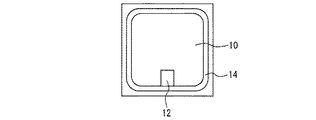
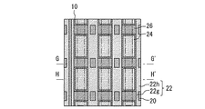
図1は、実施の形態1に係る半導体装置の平面図である。ウエハに複数の半導体装置が形成され、そのうちの1つの半導体装置が図1に示されている。この半導体装置が1つのIGBTチップを構成している。半導体装置は、素子領域10と、ゲートパッド領域12と、素子領域10及びゲートパッド領域12を囲む耐圧保持領域14を備えている。ゲートパッド領域12に印加された電圧に応じて素子領域10に電流が流れるか否かが決まる。耐圧保持領域14は、空乏層を素子領域10の外側に伸ばすために形成される。
Embodiment 1.
FIG. 1 is a plan view of the semiconductor device according to the first embodiment. A plurality of semiconductor devices are formed on the wafer, and one of the semiconductor devices is shown in FIG. This semiconductor device constitutes one IGBT chip. The semiconductor device includes an
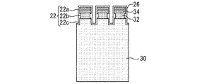
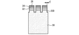
図2は、図1の素子領域10の一部を拡大した平面図である。素子領域には直線的なゲート電極20が複数設けられている。ゲート電極20は例えばポリシリコンである。ゲート電極20にはゲート絶縁膜22が接している。ゲート絶縁膜22に拡散層24とエミッタ層26が接している。図2において斜線が引かれた部分も拡散層24の一部である。斜線が引かれた部分は第2導電型の不純物濃度が中央部に比べて低くなっている。拡散層24はp型の導電型であり、エミッタ層26はn型の導電型である。以後、n型を第1導電型と称し、p型を第2導電型と称する。各部分の導電型を反転させてもよい。図2における破線で囲まれた領域はエミッタコンタクト領域28である。
FIG. 2 is an enlarged plan view of a part of the
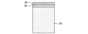
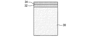
図3は、図2のA−A´線における断面図である。基板30はドリフト層として機能する部分である。基板30は例えば第1導電型のSiである。基板はn−型の導電型を有する。基板30の上面側には第1導電型のキャリアストア層32が設けられている。キャリアストア層32の上に第2導電型のチャネルドープ層34が設けられている。チャネルドープ層34の上に第1導電型のエミッタ層26が設けられている。キャリアストア層32、チャネルドープ層34、エミッタ層26はそれぞれ、n型、p型、N+型の層である。
FIG. 3 is a cross-sectional view taken along the line AA'of FIG. The
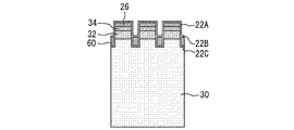
ゲート電極20は、ゲート絶縁膜22を介して、エミッタ層26、チャネルドープ層34、キャリアストア層32及び基板30と接する。ゲート絶縁膜22は、エミッタ層26とチャネルドープ層34に接する第1部分22aと、キャリアストア層32に接する第2部分22bと、基板30に接する第3部分22cとを有している。第2部分22bの少なくとも一部は、第1部分22a及び第3部分22cよりも厚い。言いかえれば、ゲート電極20とキャリアストア層32に挟まれた部分に、ゲート絶縁膜22の最も厚い部分がある。
The
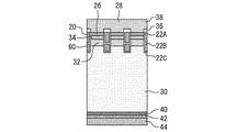
エミッタ層26の上にはエミッタ層26に接するエミッタ電極38が設けられている。エミッタ電極38とゲート電極20の間には層間絶縁膜36が設けられているので、エミッタ電極38とゲート電極20は電気的に絶縁されている。
An
基板30の下面側には、第1導電型のバッファ層40が形成されている。バッファ層40はn型の層とすることができる。バッファ層40の下面側には第2導電型のコレクタ層42が形成されている。コレクタ層42はp+型の層とすることができる。コレクタ層42の下面側にはコレクタ電極44が形成されている。基板30の下面側の構造として、コレクタ層42を有する別の構造を採用してもよい。
A first conductive
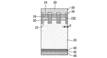
図4は、図2のB−B´線における断面図である。チャネルドープ層34の上には拡散層24が設けられている。拡散層24は、エミッタ層26に隣接する第2導電型の層である。拡散層24はp+型の層とすることができる。ゲート絶縁膜22は、拡散層24と拡散層24の下のチャネルドープ層34とに接する第4部分22dと、拡散層24の下のキャリアストア層32に接する第5部分22eと、拡散層24の下の基板30に接する第6部分22fとを有している。そして、第5部分22eの少なくとも一部は第4部分22d及び第6部分22fよりも厚い。言いかえれば、ゲート電極20とキャリアストア層32に挟まれた部分に、ゲート絶縁膜22の最も厚い部分がある。図4の第5部分22eは図3の第2部分22bと同じ形状を有している。
FIG. 4 is a cross-sectional view taken along the line BB'of FIG. A
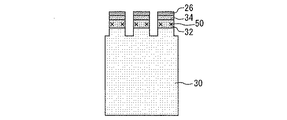
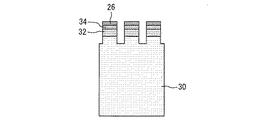
実施の形態1に係る半導体装置の製造方法を説明する。まず、基板30の上にキャリアストア層32を形成し、キャリアストア層32の上にチャネルドープ層34を形成し、チャネルドープ層34の上にエミッタ層26を形成する。その後、エミッタ層26、チャネルドープ層34およびキャリアストア層32の一部をエッチングすることで溝を形成し、基板30を露出させる。図5は、基板30を露出させる溝が形成された半導体装置の断面図である。
A method of manufacturing a semiconductor device according to the first embodiment will be described. First, the
次いで、キャリアストア層32の側壁部分にイオン注入する。例えば一般的な写真製版技術とイオン注入技術を用いて、キャリアストア層32の側壁部分にイオン注入を行う。図6は、キャリアストア層32の側壁部分にイオン注入部50が形成されたことを示す半導体装置の断面図である。局所的にイオン注入することでイオン注入部50を形成する目的は酸化レートを高めることである。
Next, ions are implanted into the side wall portion of the
次いで、キャリアストア層32の側壁部分と、チャネルドープ層34の側壁部分と、エミッタ層26の側壁部分と、基板30にゲート絶縁膜を形成する。図7は、ゲート絶縁膜22が形成された半導体装置の断面図である。ゲート絶縁膜22は、例えば高温で酸化を行う方法である熱酸化によって形成する。キャリアストア層32にはイオン注入部50が形成されているのでこの部分で特に酸化が進行する。その結果、ゲート絶縁膜22のうち第2部分22bが一番厚く形成される。次いで、ゲート絶縁膜22に接するゲート電極20を形成する。その後周知のプロセスを経て、図1−4に示す半導体装置が完成する。
Next, a gate insulating film is formed on the side wall portion of the
次に、実施の形態1に係る半導体装置の動作を説明する。半導体装置をオンにして導通状態にする場合は、ゲート電極20に正電圧を印加する。すると、エミッタ層26、チャネルドープ層34、キャリアストア層32、ゲート絶縁膜22及びゲート電極20からなるMOSFETがオンして、エミッタ電極38から電子が、コレクタ電極44から正孔が基板30へ流入し、基板30にキャリアが溜まることで導電率変調が起こる。これにより、コレクタ−エミッタ間電圧が下がり、半導体装置が導通状態となる。
Next, the operation of the semiconductor device according to the first embodiment will be described. When the semiconductor device is turned on to make it conductive, a positive voltage is applied to the
一方、半導体装置をオフ状態とするときには、ゲート電極20の電圧を、エミッタ層26、チャネルドープ層34、キャリアストア層32、ゲート絶縁膜22及びゲート電極20からなるMOSFETのしきい値電圧以下にする。そうするとエミッタ電極38とコレクタ電極44から基板30へ流入するキャリアが遮断され、基板30の内部に溜まった過剰キャリアが排出され、基板30が空乏化することで半導体装置がオフ状態となる。実施の形態1に係る半導体装置がインバータ回路の一部として設けられた場合、半導体装置のオンオフが繰り返される。
On the other hand, when the semiconductor device is turned off, the voltage of the
半導体装置をオンする際、基板30の電圧変化又は前述のMOSFETのチャネルを流れる電流変化などにより、容量成分として働くゲート絶縁膜22から変位電流が流れる。特に不純物濃度が高いキャリアストア層32とゲート絶縁膜22の界面に電流が集まりやすいので、キャリアストア層32が電流変化の影響を受けて発振などの望まない動作を引き起こす場合がある。上記の望まない動作の例としては、短絡時のゲートの浮きあがり、ターンオン時にdV/dtの値が高くなることなどが挙げられる。これに対し、実施の形態1では、キャリアストア層32に接する第2部分22bを厚くすることで変位電流自体を低下させることができる。よって、誤動作などの望まない動作を起こりにくくすることができる。
When the semiconductor device is turned on, a displacement current flows from the
さらに、キャリアストア層32を設けたことで、半導体装置をオンするときの基板30のキャリア蓄積効果が高くなるためオン電圧が小さくなる。よって、半導体装置でインバータ回路を構成した際の定常損失を下げることができる。これらの効果は、第2部分22bの厚く形成された部分がキャリアストア層32の一部と接しているだけでも得られるものである。なお、ゲート絶縁膜22のうち厚く形成された部分が基板30に接する部分にまで及んでいてもよい。
Further, by providing the
ゲート絶縁膜22の第1部分22aの厚さは、半導体装置のMOSFETのチャネル電流を決める。したがって第1部分22aの厚さは予め定められた厚さとしなければならないが、第2部分22bの厚い部分を第1部分22aに近接させると、製造ばらつきによって、第1部分22aまで厚く形成されてしまうおそれがある。そこで、第2部分22bのうち第1部分22a及び第3部分22cよりも厚い部分は、第1部分22aから離すことが好ましい。実施の形態1では、第2部分22bの中央部だけが第1部分22a及び第3部分22cよりも厚い。これにより、製造ばらつきを考慮しても、第1部分22aが厚くなってしまうことを回避できる。
The thickness of the
実施の形態1に係る半導体装置と半導体装置の製造方法はその特徴を失わない範囲で様々な変形が可能である。以下の実施の形態にかかる半導体装置、半導体装置の製造方法については、実施の形態1との共通点が多いので実施の形態1との相違点を中心に説明する。 The semiconductor device and the method for manufacturing the semiconductor device according to the first embodiment can be variously modified as long as the characteristics are not lost. Since the semiconductor device and the method for manufacturing the semiconductor device according to the following embodiments have much in common with the first embodiment, the differences from the first embodiment will be mainly described.
実施の形態2.
実施の形態2に係る半導体装置の平面図は図1、2と同じであるので省略する。図8は、実施の形態2に係る半導体装置の断面図である。この断面図は半導体装置のエミッタ層26がある部分における断面図であるので、図2のA−A´線における断面図に対応するということができる。ゲート電極20は、ゲート絶縁膜22Aを介して、エミッタ層26、チャネルドープ層34及びキャリアストア層32と接している。ゲート電極20の上面はゲート配線につながれる部分を除いて層間絶縁膜36に覆われている。ゲート電極20の側面はゲート絶縁膜22Aに覆われている。ゲート電極20の下面は分離絶縁膜22Bに覆われている。
Embodiment 2.
The plan view of the semiconductor device according to the second embodiment is the same as that of FIGS. 1 and 2, and is omitted. FIG. 8 is a cross-sectional view of the semiconductor device according to the second embodiment. Since this cross-sectional view is a cross-sectional view of a portion of the semiconductor device where the
分離絶縁膜22Bの下には導体層60が設けられている。導体層60は、ゲート電極20の直下にゲート電極20と同じ幅で形成されている。導体層60はアイソレーション絶縁膜22Cを介してキャリアストア層32と基板30に接している。導体層60の上面は分離絶縁膜22Bに覆われ、側面と下面はアイソレーション絶縁膜22Cに覆われている。導体層60は分離絶縁膜22Bとアイソレーション絶縁膜22Cに囲まれることで他の導体と電気的に絶縁されている。つまり、導体層60の電位はフローティングとなっている。導体層60の全体をアイソレーション絶縁膜22Cと分離絶縁膜22Bによって覆うことが好ましい。
A
図9は、実施の形態2に係る半導体装置の拡散層24がある部分における断面図である。図9は、図2のB−B´線における断面図に対応するということができる。拡散層24がある部分についても、ゲート絶縁膜22A、分離絶縁膜22B、アイソレーション絶縁膜22C、ゲート電極20及び導体層60が設けられている。これらは図8のゲート絶縁膜22A、分離絶縁膜22B、アイソレーション絶縁膜22C、ゲート電極20及び導体層60とつながっている。
FIG. 9 is a cross-sectional view of a portion of the semiconductor device according to the second embodiment where the
このように、実施の形態2に係る半導体装置には、ゲート電極20の下面を覆うとともに導体層60の上面を覆うことで導体層60とゲート電極20を電気的に分離する分離絶縁膜22Bがある。分離絶縁膜22Bの高さと、キャリアストア層32の中間の高さとを等しくすることが好ましい。すなわち、キャリアストア層32の上面と下面の中間位置の横に分離絶縁膜22Bを設けることが好ましい。分離絶縁膜22Bより下にあるキャリアストア層32又は基板30からみたゲート電極20の容量は、アイソレーション絶縁膜22Cと分離絶縁膜22Bの容量の直列和になるため、実効的な容量を低減することができる。このため、キャリアストア層32又は基板30の電位変動に対して生じる変位電流が少なくなる。結果として、ゲート電位の変動を抑える事ができる。キャリアストア層32の横に分離絶縁膜22Bを設けることでこの効果が得られる。
As described above, in the semiconductor device according to the second embodiment, the separating insulating
実施の形態2に係る半導体装置の製造方法を、断面図である図10−14を参照して説明する。まず、周知の方法で図10に示す構成を製造する。図10は製造途中の半導体装置の断面図である。図10に示されるように、基板30の上にキャリアストア層32を形成し、キャリアストア層32の上にチャネルドープ層34を形成し、チャネルドープ層34の上にエミッタ層26を形成する。次いで、エミッタ層26とチャネルドープ層34とキャリアストア層32に基板30が露出する溝を形成し、その溝に露出した部分にアイソレーション絶縁膜22Cを形成し、その溝を導体層60で埋め込む。アイソレーション絶縁膜22Cは例えばシリコン酸化膜である。導体層60は例えばポリシリコンである。
A method of manufacturing the semiconductor device according to the second embodiment will be described with reference to FIGS. 10-14, which are cross-sectional views. First, the configuration shown in FIG. 10 is manufactured by a well-known method. FIG. 10 is a cross-sectional view of a semiconductor device in the process of being manufactured. As shown in FIG. 10, the
次いで、図11に示す構造を製造する。図11には、導体層60の一部を除去したことが示されている。この工程では選択的に導体層60の一部をエッチバックする。導体層60の上面はキャリアストア層32の横にある。次いで、図12に示す構造を製造する。図12には、アイソレーション絶縁膜22Cの一部を選択的に除去したことが示されている。まず、図11で説明したとおり導体層60の一部を除去して、その後アイソレーション絶縁膜22Cの一部を除去することで、エミッタ層26の側面と、チャネルドープ層34の側面と、キャリアストア層32の側面の一部とを露出させる。
Next, the structure shown in FIG. 11 is manufactured. FIG. 11 shows that a part of the
次いで、ゲート酸化を行うことで図13に示す構造を製造する。図13には、導体層60の上面に分離絶縁膜22Bを形成し、エミッタ層26の側面と、チャネルドープ層34の側面と、キャリアストア層32の側面の一部にゲート絶縁膜22Aを形成したことが示されている。1回の酸化処理によって、分離絶縁膜22Bとゲート絶縁膜22Aを形成することができる。
Next, the structure shown in FIG. 13 is manufactured by performing gate oxidation. In FIG. 13, a
次いで、図14に示すように、分離絶縁膜22Bの上にある溝をゲート電極20で埋め込む。ゲート電極20は例えばポリシリコンのデポジションとその選択的なエッチバックによって形成することができる。その後、周知の方法でプロセスを進め、図8、9に示す半導体装置を完成させる。
Next, as shown in FIG. 14, the groove on the separating insulating
実施の形態3.
図15は実施の形態3に係る半導体装置の平面図である。ゲート絶縁膜22は、第1ゲート絶縁膜22Dと、第1ゲート絶縁膜22Dにつながっている第2ゲート絶縁膜22Eとを備えている。第1ゲート絶縁膜22Dはエミッタ層26に接し、第2ゲート絶縁膜22Eは拡散層24に接している。第1ゲート絶縁膜22Dと第2ゲート絶縁膜22Eのx軸に沿った長さが第1ゲート絶縁膜22Dと第2ゲート絶縁膜22Eの厚みである。第2ゲート絶縁膜22Eは第1ゲート絶縁膜22Dより厚くなっている。すなわち、半導体装置をオン状態としたときにチャネルが形成される部分に接するゲート絶縁膜よりも、チャネルが形成されない部分に接するゲート絶縁膜が厚くなっている。第2ゲート絶縁膜22Eが第1ゲート絶縁膜22Dより厚くなっている分だけ、拡散層24はエミッタ層26よりもx軸に沿った長さが短くなっている。したがって、平面視で拡散層24はエミッタ層26よりも幅が小さい。
Embodiment 3.
FIG. 15 is a plan view of the semiconductor device according to the third embodiment. The
図16は、図15のC−C´線に沿った半導体装置の断面図である。第1ゲート絶縁膜22Dは、エミッタ層26と、エミッタ層26の下のチャネルドープ層34と、エミッタ層26の下のキャリアストア層32と、基板30に接している。第1ゲート絶縁膜22Dの幅はx1である。図17は、図15のD−D´線に沿った半導体装置の断面図である。第2ゲート絶縁膜22Eは、拡散層24と、拡散層24の下のチャネルドープ層34と、拡散層24の下のキャリアストア層32と、基板30に接している。第2ゲート絶縁膜22Eの幅x2は、第1ゲート絶縁膜22Dの幅x1より大きい。ゲート電極20は第1ゲート絶縁膜22Dと第2ゲート絶縁膜22Eの両方に接する。
FIG. 16 is a cross-sectional view of the semiconductor device along the CC'line of FIG. The first
このように、第2ゲート絶縁膜22Eを第1ゲート絶縁膜22Dより厚くすることで、ゲートエミッタ間容量Cgeとゲートコレクタ間容量Cgcの値を下げることができる。これにより、ゲート絶縁膜22の周辺の電位が変動したことでゲート電極に流れる変位電流を減少させることができるので、ゲート浮きあがりによる短絡電流の増加等を防ぐ事ができる。しかも、チャネルの形成に寄与する第1ゲート絶縁膜22Dは予め定められた厚さにすることができる。
By making the second
実施の形態3に係る半導体装置の製造方法を説明する。まず、図18、19に示す構造を製造する。図18は、エミッタ層26を含む部分における断面図である。図18は、図15のC−C´線に沿った断面における製造途中の半導体装置を示す。図19は、拡散層24が形成される部分における断面図である。図19は、図15のD−D´線に沿った断面における製造途中の半導体装置を示す。基板30の上にキャリアストア層32を形成し、キャリアストア層32の上にチャネルドープ層34を形成し、チャネルドープ層34の上の一部にエミッタ層26を形成する。こうして、図18、19の構造を得ることができる。
The method of manufacturing the semiconductor device according to the third embodiment will be described. First, the structures shown in FIGS. 18 and 19 are manufactured. FIG. 18 is a cross-sectional view of a portion including the
次いで、図18、19に示す構造に、ゲート絶縁膜とゲート電極を形成するための溝を形成する。図20は、溝形成に用いる写真製版用のマスク70の平面図である。マスク70は第1部分70Aと第2部分70Bを備えている。第1部分70Aでは直線的なマスクパターンとなっているが、第2部分70Bでは蛇腹状のマスクパターンとなっている。レジストを塗布した半導体装置のレジストにマスク70を用いて露光処理をし、露光されたレジストを現像し、レジストパターンから露出した部分を基板30が露出するまでエッチングする。そうすると、図21、22で示す構造を得ることができる。
Next, a groove for forming the gate insulating film and the gate electrode is formed in the structure shown in FIGS. 18 and 19. FIG. 20 is a plan view of the
図21は、エミッタ層26がある部分における半導体装置の断面図である。図21は図18と同じ位置における断面図である。図22は、エミッタ層26がない部分における半導体装置の断面図である。図22は図19と同じ位置における断面図である。マスク70を利用したエッチングにより、平面視でエミッタ層26が形成された部分に、側面が平面視で直線となり、基板30が露出する溝が形成される。したがって、図21の溝の幅は一様である。また、平面視でエミッタ層26が形成されていない部分に、側面が平面視で蛇腹となり、基板30が露出する溝も形成される。したがって、図22の溝は、マスク70の第2部分70Bにおける蛇腹状の形状を反映して、場所により幅が異なっている。
FIG. 21 is a cross-sectional view of the semiconductor device in the portion where the
次いで、図21、22に示す構造に熱酸化を施す。具体的には、エミッタ層26、チャネルドープ層34及びキャリアストア層32の側面と、溝に露出した基板30とを熱酸化してゲート絶縁膜を形成する。図23、24は、図21、22に示す構造を熱酸化して得られた構造の断面図である。熱酸化では、平面視で蛇腹状に形成された部分では3方向から酸化が進む。つまり、図15の座標系で言えば、x正方向又はx負方向、並びにy正方向及びy負方向に酸化が進む。熱酸化では、3方向から進展した酸化膜がつながって蛇腹状の部分のシリコンが無くなるまで酸化を進める。こうして、図23、24に示すように、エミッタ層26に接する第1ゲート絶縁膜22Dよりも、拡散層24に接する第2ゲート絶縁膜22Eを厚くすることができる。その後、ゲート絶縁膜22に接するゲート電極20を形成し、周知のプロセスを実行することで、トレンチ型のゲート部を有する半導体装置を製造することができる。
Next, the structures shown in FIGS. 21 and 22 are subjected to thermal oxidation. Specifically, the side surfaces of the
実施の形態4.
実施の形態4に係る半導体装置の平面図は図1、2と同じであるので省略する。図25、26は、実施の形態4に係る半導体装置の断面図である。図25は半導体装置のエミッタ層26がある部分における断面図なので、図2のA−A´線における断面図に対応するということができる。図26は半導体装置の拡散層24がある部分における断面図なので、図2のB−B´線における断面図に対応するということができる。
Embodiment 4.
The plan view of the semiconductor device according to the fourth embodiment is the same as that of FIGS. 1 and 2, and is omitted. 25 and 26 are cross-sectional views of the semiconductor device according to the fourth embodiment. Since FIG. 25 is a cross-sectional view of a portion of the semiconductor device where the
図25には、ゲート絶縁膜22を介して、エミッタ層26、チャネルドープ層34、キャリアストア層32及び基板30と接するゲート電極20が示されている。ゲート電極20は、基板30の上面側の第1ゲート電極20Aと、第1ゲート電極20Aの下面に接し、第1ゲート電極20Aよりも不純物濃度が小さい第2ゲート電極20Bとを有している。第1ゲート電極20Aと第2ゲート電極20Bは例えばドープドポリシリコンである。第1ゲート電極20Aと第2ゲート電極20Bの境界は、キャリアストア層32の横にある。図26に示されるように、拡散層24がある部分でも、図25と同じく第1ゲート電極20Aと第2ゲート電極20Bを有するゲート電極20が設けられている。
FIG. 25 shows the
図25、26に示す半導体装置は、まず、第2ゲート電極20Bの材料を堆積させ、その一部を選択的にエッチバックした後、第1ゲート電極20Aの材料を堆積する事で形成できる。ゲート電極20のコレクタ側に形成された部分である第2ゲート電極20Bを、第1ゲート電極20Aよりも低不純物濃度とした。これは、ゲート絶縁膜22を介してキャリアストア層32及び基板30に接するゲート電極20の不純物濃度を低濃度にすることと言い換えることができる。これにより、第2ゲート電極20Dに電位分布が生じ変位電流が減少する。よって、チャネルが形成される部分の横にあるゲート電極20の電位変動が小さくなり、ゲート電位の浮きあがりによる短絡電流増加および低電流ターンオン時のリカバリ電流等を抑制できる。
The semiconductor device shown in FIGS. 25 and 26 can be formed by first depositing the material of the
実施の形態5.
図27は実施の形態5に係る半導体装置の平面図である。ゲート電極20は平面視でエミッタ層26の横にだけ形成されている。拡散層24の横にはゲート電極20は形成されていない。平面視するとゲート電極20は島状に複数形成されている。エミッタ層26の横の第1ゲート絶縁膜22gよりも、拡散層24の横の第2ゲート絶縁膜22hが厚く形成されている。これにより、チャネルの形成される部分であるエミッタ層26の横にのみゲート電極20が設けられる。
Embodiment 5.
FIG. 27 is a plan view of the semiconductor device according to the fifth embodiment. The
図28は、図27のG−G´線における半導体装置の断面図である。ゲート電極20の上にゲート配線80が形成されている。図29は、図27のH−H´線における半導体装置の断面図である。第2ゲート絶縁膜22hの上にはゲート配線80が形成されている。図28のゲート配線80と図29のゲート配線80はつながっている。ゲート電極20とゲート配線80は例えばポリシリコンである。
FIG. 28 is a cross-sectional view of the semiconductor device on the GG'line of FIG. 27. The
このように、チャネルが形成されない部分である拡散層24に接するゲート絶縁膜を厚くすることで、CgeとCgcの値を下げることができる。これによりゲート絶縁膜の周辺で電位変動が起こった際にゲート電極20に生じる変位電流が減少し、ゲート浮きあがりによる短絡電流の増加等を防ぐ事ができる。
In this way, by thickening the gate insulating film in contact with the
実施の形態5に係る半導体装置の製造方法を説明する。まず、図30、31に示す構造を製造する。図30は、エミッタ層26を含む部分における半導体装置の断面図である。図30は、図27のG−G´線に沿った断面における製造途中の半導体装置を示す。図31は、拡散層24が形成される部分における断面図である。図31は、図27のH−H´線に沿った断面における製造途中の半導体装置を示す。基板30の上にキャリアストア層32を形成し、キャリアストア層32の上にチャネルドープ層34を形成し、チャネルドープ層34の上の一部にエミッタ層26を形成する。こうして、図30、31の構造を得ることができる。
The method of manufacturing the semiconductor device according to the fifth embodiment will be described. First, the structures shown in FIGS. 30 and 31 are manufactured. FIG. 30 is a cross-sectional view of the semiconductor device in the portion including the
次いで、図30、31に示す構造に、ゲート絶縁膜とゲート電極を形成するための溝を形成する。具体的には、平面視でエミッタ層26が形成された部分と、平面視でエミッタ層26が形成されていない部分の一部をエッチングして基板30を露出させる第1溝を形成する。図32、33には、第1溝82が示されている。図32は、図30の構造に第1溝82を形成したことを示す断面図である。図33は、図31の構造に第1溝82を形成したことを示す断面図である。第1溝82は、一般的な写真製版技術とエッチング技術を用いて形成することができる。
Next, a groove for forming the gate insulating film and the gate electrode is formed in the structures shown in FIGS. 30 and 31. Specifically, a first groove is formed by etching a part where the
次いで、第1溝82をゲート絶縁膜で埋め込む。例えば、酸化膜を堆積させた後で、余分の酸化膜をエッチングで除去することで、第1溝82の内にゲート絶縁膜を形成する。図34は、図32の構造における第1溝82に第1ゲート絶縁膜22gを形成したことを示す断面図である。図35は、図33の構造における第1溝82に第2ゲート絶縁膜22hを形成したことを示す断面図である。
Next, the
次いで、図34に示す第1ゲート絶縁膜22gに第2溝を形成する。そしてその第2溝をゲート電極で埋め込む。図36には、図34の構造に第2溝84を形成しその第2溝84をゲート電極20で埋め込んだことが示されている。第2溝84は、平面視でエミッタ層26の横にある第1ゲート絶縁膜22gの一部を、エミッタ層26とチャネルドープ層34とキャリアストア層32と基板30を露出させないように、エッチングすることで形成する。このプロセスは、一般的な写真製版技術とエッチング技術を用いて行うことができる。その結果、断面視でU字型の第1ゲート絶縁膜22gが形成される。断面視でU字型に形成された第1ゲート絶縁膜22gによって第2溝84が提供される。この第2溝84に例えばポリシリコンでゲート電極20を形成する。
Next, a second groove is formed in the first
このゲート電極20の形成と同時に又は遅れて、ゲート電極20の上にゲート配線80を形成する。図37に示すように、第2ゲート絶縁膜22hの上にもゲート配線80を形成する。平面視でエミッタ層26の横と、エミッタ層26が形成されていない部分の横とにゲート配線80を形成することで、拡散層24を挟んで設けられた2つのエミッタ層26に隣接するゲート電極20を電気的に接続することができる。堆積技術と写真製版及びエッチングの技術とを用いることで、第2溝84を形成し、ゲート電極20を形成し、ゲート配線80を形成することができる。その後、周知のプロセスを実行することで、図27−29に示された半導体装置を製造することができる。
At the same time as or after the formation of the
実施の形態6.
図38は実施の形態6に係る半導体装置の平面図である。エミッタ層26は平面視で千鳥状に複数設けられている。拡散層24は平面視で千鳥状に複数設けられている。並行に走っているゲート電極20に対して、エミッタ層26と拡散層24が千鳥形に配置されている。ゲート絶縁膜22は、エミッタ層26に接する第1ゲート絶縁膜22Fと、拡散層24に接する第2ゲート絶縁膜22Gを備えている。第2ゲート絶縁膜22Gの少なくとも一部は、第1ゲート絶縁膜22Fよりも厚く形成されている。
Embodiment 6.
FIG. 38 is a plan view of the semiconductor device according to the sixth embodiment. A plurality of emitter layers 26 are provided in a staggered manner in a plan view. A plurality of diffusion layers 24 are provided in a staggered manner in a plan view. The
図39は、図38のI−I´線における断面図である。第2ゲート絶縁膜22Gの厚さx2は第1ゲート絶縁膜22Fの厚さx1より大きい。つまり、チャネルが形成されない拡散層24に接するゲート絶縁膜を、チャネルが形成されるエミッタ層26に接するゲート絶縁膜より厚くする。これにより、CgeとCgcの値を下げることができる。そうすると、ゲート絶縁膜周辺で電位変動が起こった際のゲート電極の変位電流が減少し、ゲート浮きあがりによる短絡電流の増加等を防ぐ事ができる。
FIG. 39 is a cross-sectional view taken along the line I-I'of FIG. 38. The thickness x2 of the second gate insulating film 22G is larger than the thickness x1 of the first
実施の形態3に係る半導体装置の製造方法と同様に蛇腹状のパターンを形成して酸化膜の厚さに差をつける手法を利用することで、実施の形態6に係る半導体装置を製造することができる。 The semiconductor device according to the sixth embodiment is manufactured by using the method of forming a bellows-shaped pattern to make a difference in the thickness of the oxide film in the same manner as the manufacturing method of the semiconductor device according to the third embodiment. Can be done.
実施の形態3、5、6の半導体装置は、拡散層24に接するゲート絶縁膜の少なくとも一部を、エミッタ層26に接するゲート絶縁膜よりも厚くした点で共通している。この特徴を別の実施形態に取り入れてもよい。
The semiconductor devices of the third, fifth, and sixth embodiments are common in that at least a part of the gate insulating film in contact with the
実施の形態1−6で説明した半導体装置の特徴を組み合わせて、本発明の効果を高めてもよい。半導体装置のある領域にある実施形態の構造を採用し、別の領域に別の実施形態の構造を採用してもよい。部分的に上記の構造を採用してもよい。また、半導体装置の構造としてはIGBTに限定されず、MOSFETまたはダイオードなどのパワーデバイスとしてもよい。半導体装置の耐圧クラスは特に限定されない。基板30としては、FZ基板、エピ基板又は周知の基板を用いることができる。
The effects of the present invention may be enhanced by combining the features of the semiconductor device described in the first to sixth embodiments. The structure of the embodiment in one region of the semiconductor device may be adopted and the structure of another embodiment may be adopted in another region. The above structure may be partially adopted. Further, the structure of the semiconductor device is not limited to the IGBT, and may be a power device such as a MOSFET or a diode. The withstand voltage class of the semiconductor device is not particularly limited. As the
実施の形態7.
本実施の形態は、上述した実施の形態1−6にかかる半導体装置を電力変換装置に適用したものである。本発明は特定の電力変換装置に限定されるものではないが、以下、実施の形態7として、三相のインバータに本発明を適用した場合について説明する。
Embodiment 7.
In this embodiment, the semiconductor device according to the above-described first to sixth embodiments is applied to a power conversion device. Although the present invention is not limited to a specific power conversion device, the case where the present invention is applied to a three-phase inverter will be described below as a seventh embodiment.
図40は、本実施の形態にかかる電力変換装置を適用した電力変換システムの構成を示すブロック図である。 FIG. 40 is a block diagram showing a configuration of a power conversion system to which the power conversion device according to the present embodiment is applied.
図40に示す電力変換システムは、電源100、電力変換装置200、負荷300から構成される。電源100は、直流電源であり、電力変換装置200に直流電力を供給する。電源100は種々のもので構成することが可能であり、例えば、直流系統、太陽電池、蓄電池で構成することができるし、交流系統に接続された整流回路又はAC/DCコンバータで構成することとしてもよい。また、電源100を、直流系統から出力される直流電力を所定の電力に変換するDC/DCコンバータによって構成することとしてもよい。
The power conversion system shown in FIG. 40 includes a
電力変換装置200は、電源100と負荷300の間に接続された三相のインバータであり、電源100から供給された直流電力を交流電力に変換し、負荷300に交流電力を供給する。電力変換装置200は、図40に示すように、直流電力を交流電力に変換して出力する主変換回路201と、主変換回路201の各スイッチング素子を駆動する駆動信号を出力する駆動回路202と、駆動回路202を制御する制御信号を駆動回路202に出力する制御回路203とを備えている。
The
負荷300は、電力変換装置200から供給された交流電力によって駆動される三相の電動機である。なお、負荷300は特定の用途に限られるものではなく、各種電気機器に搭載された電動機であり、例えば、ハイブリッド自動車、電気自動車、鉄道車両、エレベーター、もしくは、空調機器向けの電動機として用いられる。
The
以下、電力変換装置200の詳細を説明する。主変換回路201は、スイッチング素子と還流ダイオードを備えており(図示せず)、スイッチング素子がスイッチングすることによって、電源100から供給される直流電力を交流電力に変換し、負荷300に供給する。主変換回路201の具体的な回路構成は種々のものがあるが、本実施の形態にかかる主変換回路201は2レベルの三相フルブリッジ回路であり、6つのスイッチング素子とそれぞれのスイッチング素子に逆並列された6つの還流ダイオードから構成することができる。主変換回路201の各スイッチング素子には、上述した実施の形態1−6のいずれかにかかる半導体装置を適用する。6つのスイッチング素子は2つのスイッチング素子ごとに直列接続され上下アームを構成し、各上下アームはフルブリッジ回路の各相(U相、V相、W相)を構成する。そして、各上下アームの出力端子、すなわち主変換回路201の3つの出力端子は、負荷300に接続される。
The details of the
駆動回路202は、主変換回路201のスイッチング素子を駆動する駆動信号を生成し、主変換回路201のスイッチング素子の制御電極に供給する。具体的には、後述する制御回路203からの制御信号に従い、スイッチング素子をオン状態にする駆動信号とスイッチング素子をオフ状態にする駆動信号とを各スイッチング素子の制御電極に出力する。スイッチング素子をオン状態に維持する場合、駆動信号はスイッチング素子の閾値電圧以上の電圧信号(オン信号)であり、スイッチング素子をオフ状態に維持する場合、駆動信号はスイッチング素子の閾値電圧以下の電圧信号(オフ信号)となる。
The
制御回路203は、負荷300に所望の電力が供給されるよう主変換回路201のスイッチング素子を制御する。具体的には、負荷300に供給すべき電力に基づいて主変換回路201の各スイッチング素子がオン状態となるべき時間(オン時間)を算出する。例えば、出力すべき電圧に応じてスイッチング素子のオン時間を変調するPWM制御によって主変換回路201を制御することができる。そして、各時点においてオン状態となるべきスイッチング素子にはオン信号を、オフ状態となるべきスイッチング素子にはオフ信号が出力されるよう、駆動回路202に制御指令(制御信号)を出力する。駆動回路202は、この制御信号に従い、各スイッチング素子の制御電極にオン信号又はオフ信号を駆動信号として出力する。
The
本実施の形態に係る電力変換装置では、主変換回路201のスイッチング素子として実施の形態1−6のいずれか1つにかかる半導体装置を適用するため、ゲート電極に流れる変位電流を原因とする誤動作を防止できる。つまり、電力変換装置の信頼性を高めることができる。
In the power conversion device according to the present embodiment, since the semiconductor device according to any one of the first to sixth embodiments is applied as the switching element of the
本実施の形態では、2レベルの三相インバータに本発明を適用する例を説明したが、本発明は、これに限られるものではなく、種々の電力変換装置に適用することができる。本実施の形態では、2レベルの電力変換装置としたが3レベル又はマルチレベルの電力変換装置であっても構わないし、単相負荷に電力を供給する場合には単相のインバータに本発明を適用しても構わない。また、直流負荷等に電力を供給する場合にはDC/DCコンバータ又はAC/DCコンバータに本発明を適用することも可能である。 In the present embodiment, an example of applying the present invention to a two-level three-phase inverter has been described, but the present invention is not limited to this, and can be applied to various power conversion devices. In the present embodiment, a two-level power conversion device is used, but a three-level or multi-level power conversion device may be used, and when power is supplied to a single-phase load, the present invention is applied to a single-phase inverter. You may apply it. Further, when supplying electric power to a DC load or the like, the present invention can be applied to a DC / DC converter or an AC / DC converter.
また、本発明を適用した電力変換装置は、上述した負荷が電動機の場合に限定されるものではなく、例えば、放電加工機若しくはレーザー加工機、又は誘導加熱調理器若しくは非接触器給電システムの電源装置として用いることもでき、さらには太陽光発電システム又は蓄電システム等のパワーコンディショナーとして用いることも可能である。 Further, the power conversion device to which the present invention is applied is not limited to the case where the above-mentioned load is an electric motor, for example, a power source for an electric discharge machine or a laser machine, or an induction heating cooker or a non-contact power supply system. It can be used as a device, and can also be used as a power conditioner for a photovoltaic power generation system, a power storage system, or the like.
10 素子領域、 20 ゲート電極、 22 ゲート絶縁膜、 24 拡散層、 26 エミッタ層、 30 基板、 32 キャリアストア層、 34 チャネルドープ層、 38 エミッタ電極、 40 バッファ層、 42 コレクタ層、 44 コレクタ電極 10 element regions, 20 gate electrodes, 22 gate insulating film, 24 diffuse layers, 26 emitter layers, 30 substrates, 32 carrier store layers, 34 channel-doped layers, 38 emitter electrodes, 40 buffer layers, 42 collector layers, 44 collector electrodes
Claims (17)
前記基板の上面側に形成された第1導電型のキャリアストア層と、
前記キャリアストア層の上に形成された第2導電型のチャネルドープ層と、
前記チャネルドープ層の上に形成された第1導電型のエミッタ層と、
ゲート絶縁膜を介して、前記エミッタ層、前記チャネルドープ層及び前記キャリアストア層と接するゲート電極と、
前記基板の下面側に形成された第2導電型のコレクタ層と、を備え、
前記ゲート絶縁膜は、前記エミッタ層と前記チャネルドープ層に接する第1部分と、前記キャリアストア層に接する第2部分と、前記基板に接する第3部分とを有し、
前記第2部分の少なくとも一部は、前記第1部分及び前記第3部分よりも厚く、
前記第2部分の中央部だけが前記第1部分及び前記第3部分よりも厚いことを特徴とする半導体装置。 The first conductive type substrate and
A first conductive type carrier store layer formed on the upper surface side of the substrate, and
A second conductive type channel-doped layer formed on the carrier store layer,
A first conductive type emitter layer formed on the channel-doped layer and
A gate electrode in contact with the emitter layer, the channel-doped layer, and the carrier store layer via a gate insulating film.
A second conductive type collector layer formed on the lower surface side of the substrate is provided.
The gate insulating film has a first portion in contact with the emitter layer and the channel-doped layer, a second portion in contact with the carrier store layer, and a third portion in contact with the substrate.
Wherein at least a portion of said second portion, rather thick than said first portion and said third portion,
A semiconductor device characterized in that only the central portion of the second portion is thicker than the first portion and the third portion .
前記基板の上面側に形成された第1導電型のキャリアストア層と、
前記キャリアストア層の上に形成された第2導電型のチャネルドープ層と、
前記チャネルドープ層の上に形成された第1導電型のエミッタ層と、
ゲート絶縁膜を介して、前記エミッタ層、前記チャネルドープ層及び前記キャリアストア層と接するゲート電極と、
前記基板の下面側に形成された第2導電型のコレクタ層と、を備え、
前記ゲート絶縁膜は、前記エミッタ層と前記チャネルドープ層に接する第1部分と、前記キャリアストア層に接する第2部分と、前記基板に接する第3部分とを有し、
前記第2部分の少なくとも一部は、前記第1部分及び前記第3部分よりも厚く、
前記チャネルドープ層の上に形成された、前記エミッタ層に隣接する第2導電型の拡散層を備え、
前記ゲート絶縁膜は、前記拡散層と前記拡散層の下の前記チャネルドープ層とに接する第4部分と、前記拡散層の下の前記キャリアストア層に接する第5部分と、前記拡散層の下の前記基板に接する第6部分とを有し、
前記第5部分の少なくとも一部は、前記第4部分及び前記第6部分よりも厚いことを特徴とする半導体装置。 The first conductive type substrate and
A first conductive type carrier store layer formed on the upper surface side of the substrate, and
A second conductive type channel-doped layer formed on the carrier store layer,
A first conductive type emitter layer formed on the channel-doped layer and
A gate electrode in contact with the emitter layer, the channel-doped layer, and the carrier store layer via a gate insulating film.
A second conductive type collector layer formed on the lower surface side of the substrate is provided.
The gate insulating film has a first portion in contact with the emitter layer and the channel-doped layer, a second portion in contact with the carrier store layer, and a third portion in contact with the substrate.
At least a part of the second part is thicker than the first part and the third part.
A second conductive type diffusion layer adjacent to the emitter layer formed on the channel-doped layer is provided.
The gate insulating film has a fourth portion in contact with the diffusion layer and the channel-doped layer under the diffusion layer, a fifth portion in contact with the carrier store layer under the diffusion layer, and under the diffusion layer. Has a sixth portion in contact with the substrate of
Wherein at least a portion of the fifth portion, a semi-conductor device you said thicker than the fourth portion and the sixth portion.
前記基板の上面側に形成された第1導電型のキャリアストア層と、 A first conductive type carrier store layer formed on the upper surface side of the substrate, and
前記キャリアストア層の上に形成された第2導電型のチャネルドープ層と、 A second conductive type channel-doped layer formed on the carrier store layer,
前記チャネルドープ層の上に形成された第1導電型のエミッタ層と、 A first conductive type emitter layer formed on the channel-doped layer and
ゲート絶縁膜を介して、前記エミッタ層、前記チャネルドープ層及び前記キャリアストア層と接するゲート電極と、 A gate electrode in contact with the emitter layer, the channel-doped layer, and the carrier store layer via a gate insulating film.
アイソレーション絶縁膜を介して、キャリアストア層と前記基板に接するフローティング電位の導体層と、 A carrier store layer and a conductor layer having a floating potential in contact with the substrate via an isolation insulating film,
前記ゲート電極の下面を覆うとともに前記導体層の上面を覆うことで前記導体層と前記ゲート電極を電気的に分離する分離絶縁膜と、 A separating insulating film that electrically separates the conductor layer from the gate electrode by covering the lower surface of the gate electrode and the upper surface of the conductor layer.
前記基板の下面側に形成された第2導電型のコレクタ層と、を備え、 A second conductive type collector layer formed on the lower surface side of the substrate is provided.
前記導体層は下面側端部が、前記アイソレーション絶縁膜を介して前記基板と対向することを特徴とする半導体装置。 A semiconductor device in which the lower end of the conductor layer faces the substrate via the isolation insulating film.
前記基板の上面側に形成された第1導電型のキャリアストア層と、 A first conductive type carrier store layer formed on the upper surface side of the substrate, and
前記キャリアストア層の上に形成された第2導電型のチャネルドープ層と、 A second conductive type channel-doped layer formed on the carrier store layer,
前記チャネルドープ層の上に形成された第1導電型のエミッタ層と、 A first conductive type emitter layer formed on the channel-doped layer and
ゲート絶縁膜を介して、前記エミッタ層、前記チャネルドープ層及び前記キャリアストア層と接するゲート電極と、 A gate electrode in contact with the emitter layer, the channel-doped layer, and the carrier store layer via a gate insulating film.
アイソレーション絶縁膜を介して、キャリアストア層と前記基板に接するフローティング電位の導体層と、 A carrier store layer and a conductor layer having a floating potential in contact with the substrate via an isolation insulating film,
前記ゲート電極の下面を覆うとともに前記導体層の上面を覆うことで前記導体層と前記ゲート電極を電気的に分離する分離絶縁膜と、 A separating insulating film that electrically separates the conductor layer from the gate electrode by covering the lower surface of the gate electrode and the upper surface of the conductor layer.
前記基板の下面側に形成された第2導電型のコレクタ層と、を備え、 A second conductive type collector layer formed on the lower surface side of the substrate is provided.
前記分離絶縁膜の高さと、前記キャリアストア層の中間の高さが等しいことを特徴とする半導体装置。 A semiconductor device characterized in that the height of the separating insulating film is equal to the height of the middle of the carrier store layer.
前記基板の上面側に形成された第1導電型のキャリアストア層と、 A first conductive type carrier store layer formed on the upper surface side of the substrate, and
前記キャリアストア層の上に形成された第2導電型のチャネルドープ層と、 A second conductive type channel-doped layer formed on the carrier store layer,
前記チャネルドープ層の上に形成された第1導電型のエミッタ層と、 A first conductive type emitter layer formed on the channel-doped layer and
前記チャネルドープ層の上に形成された、前記エミッタ層に隣接する第2導電型の拡散層と、 A second conductive diffusion layer formed on the channel-doped layer and adjacent to the emitter layer,
前記エミッタ層と、前記エミッタ層の下のチャネルドープ層と、前記エミッタ層の下のキャリアストア層に接する第1ゲート絶縁膜と、 The emitter layer, the channel-doped layer under the emitter layer, and the first gate insulating film in contact with the carrier store layer under the emitter layer.
前記拡散層と、前記拡散層の下のチャネルドープ層と、前記拡散層の下のキャリアストア層に接し、前記第1ゲート絶縁膜より厚い第2ゲート絶縁膜と、 A second gate insulating film that is in contact with the diffusion layer, a channel-doped layer under the diffusion layer, and a carrier store layer under the diffusion layer, and is thicker than the first gate insulating film.
前記第1ゲート絶縁膜に接するゲート電極と、 The gate electrode in contact with the first gate insulating film and
前記基板の下面側に形成された第2導電型のコレクタ層と、を備え、 A second conductive type collector layer formed on the lower surface side of the substrate is provided.
平面視で前記拡散層は前記エミッタ層よりも幅が小さいことを特徴とする半導体装置。 A semiconductor device characterized in that the diffusion layer has a width smaller than that of the emitter layer in a plan view.
前記基板の上面側に形成された第1導電型のキャリアストア層と、 A first conductive type carrier store layer formed on the upper surface side of the substrate, and
前記キャリアストア層の上に形成された第2導電型のチャネルドープ層と、 A second conductive type channel-doped layer formed on the carrier store layer,
前記チャネルドープ層の上に形成された第1導電型のエミッタ層と、 A first conductive type emitter layer formed on the channel-doped layer and
前記チャネルドープ層の上に形成された、前記エミッタ層に隣接する第2導電型の拡散層と、 A second conductive diffusion layer formed on the channel-doped layer and adjacent to the emitter layer,
前記エミッタ層と、前記エミッタ層の下のチャネルドープ層と、前記エミッタ層の下のキャリアストア層に接する第1ゲート絶縁膜と、 The emitter layer, the channel-doped layer under the emitter layer, and the first gate insulating film in contact with the carrier store layer under the emitter layer.
前記拡散層と、前記拡散層の下のチャネルドープ層と、前記拡散層の下のキャリアストア層に接し、前記第1ゲート絶縁膜より厚い第2ゲート絶縁膜と、 2.
前記第1ゲート絶縁膜に接するゲート電極と、 The gate electrode in contact with the first gate insulating film and
前記基板の下面側に形成された第2導電型のコレクタ層と、を備え、 A second conductive type collector layer formed on the lower surface side of the substrate is provided.
前記ゲート電極は平面視で前記エミッタ層の横にだけ形成されたことを特徴とする半導体装置。 A semiconductor device characterized in that the gate electrode is formed only beside the emitter layer in a plan view.
前記基板の上面側に形成された第1導電型のキャリアストア層と、 A first conductive type carrier store layer formed on the upper surface side of the substrate, and
前記キャリアストア層の上に形成された第2導電型のチャネルドープ層と、 A second conductive type channel-doped layer formed on the carrier store layer,
前記チャネルドープ層の上に形成された第1導電型のエミッタ層と、 A first conductive type emitter layer formed on the channel-doped layer and
前記チャネルドープ層の上に形成された、前記エミッタ層に隣接する第2導電型の拡散層と、 A second conductive diffusion layer formed on the channel-doped layer and adjacent to the emitter layer,
前記エミッタ層と、前記エミッタ層の下のチャネルドープ層と、前記エミッタ層の下のキャリアストア層に接する第1ゲート絶縁膜と、 The emitter layer, the channel-doped layer under the emitter layer, and the first gate insulating film in contact with the carrier store layer under the emitter layer.
前記拡散層と、前記拡散層の下のチャネルドープ層と、前記拡散層の下のキャリアストア層に接し、前記第1ゲート絶縁膜より厚い第2ゲート絶縁膜と、 A second gate insulating film that is in contact with the diffusion layer, a channel-doped layer under the diffusion layer, and a carrier store layer under the diffusion layer, and is thicker than the first gate insulating film.
前記第1ゲート絶縁膜に接するゲート電極と、 The gate electrode in contact with the first gate insulating film and
前記基板の下面側に形成された第2導電型のコレクタ層と、を備え、 A second conductive type collector layer formed on the lower surface side of the substrate is provided.
前記エミッタ層は、平面視で千鳥状に複数設けられ、 A plurality of the emitter layers are provided in a staggered manner in a plan view.
前記拡散層は、平面視で千鳥状に複数設けられたことを特徴とする半導体装置。 A semiconductor device characterized in that a plurality of the diffusion layers are provided in a staggered manner in a plan view.
前記基板の上面側に形成された第1導電型のキャリアストア層と、 A first conductive type carrier store layer formed on the upper surface side of the substrate, and
前記キャリアストア層の上に形成された第2導電型のチャネルドープ層と、 A second conductive type channel-doped layer formed on the carrier store layer,
前記チャネルドープ層の上に形成された第1導電型のエミッタ層と、 A first conductive type emitter layer formed on the channel-doped layer and
ゲート絶縁膜を介して、前記エミッタ層、前記チャネルドープ層及び前記キャリアストア層と接するゲート電極と、 A gate electrode in contact with the emitter layer, the channel-doped layer, and the carrier store layer via a gate insulating film.
前記基板の下面側に形成された第2導電型のコレクタ層と、を備え、 A second conductive type collector layer formed on the lower surface side of the substrate is provided.
前記ゲート電極は、前記基板の上面側の第1ゲート電極と、前記第1ゲート電極の下面に接し、前記第1ゲート電極よりも不純物濃度が小さい第2ゲート電極とを有し、 The gate electrode has a first gate electrode on the upper surface side of the substrate and a second gate electrode that is in contact with the lower surface of the first gate electrode and has a lower impurity concentration than the first gate electrode.
前記第1ゲート電極と前記第2ゲート電極の境界は、前記キャリアストア層の横にあることを特徴とする半導体装置。 A semiconductor device characterized in that the boundary between the first gate electrode and the second gate electrode is next to the carrier store layer.
前記キャリアストア層の側壁部分にイオン注入することと、 Ion implantation into the side wall of the carrier store layer
前記キャリアストア層の側壁部分と、前記チャネルドープ層の側壁部分と、前記エミッタ層の側壁部分と、前記第2導電型の拡散層と、前記基板にゲート絶縁膜を形成することと、 Forming a side wall portion of the carrier store layer, a side wall portion of the channel-doped layer, a side wall portion of the emitter layer, the second conductive type diffusion layer, and a gate insulating film on the substrate.
前記ゲート絶縁膜に接するゲート電極を形成することと、を備える半導体装置の製造方法。 A method for manufacturing a semiconductor device, comprising forming a gate electrode in contact with the gate insulating film.
前記エミッタ層と前記チャネルドープ層と前記キャリアストア層に前記基板が露出する溝を形成し、前記溝に露出した部分にアイソレーション絶縁膜を形成し、前記溝を導体層で埋め込み、前記導体層の下面側端部を前記アイソレーション絶縁膜を介して前記基板と対向させることと、 A groove in which the substrate is exposed is formed in the emitter layer, the channel-doped layer, and the carrier store layer, an isolation insulating film is formed in the portion exposed in the groove, the groove is embedded in the conductor layer, and the conductor layer is formed. The lower surface side end portion of the above is made to face the substrate via the isolation insulating film, and
前記導体層と前記アイソレーション絶縁膜の一部を除去して、前記エミッタ層の側面と、前記チャネルドープ層の側面と、前記キャリアストア層の側面の一部とを露出させることと、 By removing a part of the conductor layer and the isolation insulating film to expose the side surface of the emitter layer, the side surface of the channel-doped layer, and a part of the side surface of the carrier store layer.
前記導体層の上面に分離絶縁膜を形成し、前記エミッタ層の側面と、前記チャネルドープ層の側面と、前記キャリアストア層の側面の一部にゲート絶縁膜を形成し、前記溝をゲート電極で埋め込むことと、を備え、 A separation insulating film is formed on the upper surface of the conductor layer, a gate insulating film is formed on the side surface of the emitter layer, the side surface of the channel-doped layer, and a part of the side surface of the carrier store layer, and the groove is formed into a gate electrode. With embedding in,
前記導体層の電位をフローティングとした半導体装置の製造方法。 A method for manufacturing a semiconductor device in which the potential of the conductor layer is floating.
平面視で前記エミッタ層が形成された部分に、側面が平面視で直線となり、前記基板が露出する溝を形成し、平面視で前記エミッタ層が形成されていない部分に、側面が平面視で蛇腹となり、前記基板が露出する溝を形成することと、 In the portion where the emitter layer is formed in plan view, the side surface becomes a straight line in plan view, a groove is formed in which the substrate is exposed, and in the portion where the emitter layer is not formed in plan view, the side surface is in plan view. Forming a groove that becomes a bellows and exposes the substrate,
前記エミッタ層、前記チャネルドープ層及び前記キャリアストア層の側面と、前記溝に露出した前記基板とを熱酸化してゲート絶縁膜を形成することと、 To form a gate insulating film by thermally oxidizing the side surfaces of the emitter layer, the channel-doped layer and the carrier store layer, and the substrate exposed in the groove.
前記ゲート絶縁膜に接するゲート電極を形成することと、を備える半導体装置の製造方法。 A method for manufacturing a semiconductor device, comprising forming a gate electrode in contact with the gate insulating film.
平面視で前記エミッタ層が形成された部分と、平面視で前記エミッタ層が形成されていない部分の一部をエッチングして前記基板を露出させる第1溝を形成することと、 By etching a part where the emitter layer is formed in a plan view and a part where the emitter layer is not formed in a plan view to form a first groove for exposing the substrate.
前記第1溝をゲート絶縁膜で埋め込むことと、 By embedding the first groove with a gate insulating film,
平面視で前記エミッタ層が形成された部分の前記ゲート絶縁膜の一部を、前記エミッタ層と前記チャネルドープ層と前記キャリアストア層と前記基板を露出させないように、エッチングすることで前記ゲート絶縁膜に第2溝を形成することと、 The gate insulating film is formed by etching a part of the gate insulating film of the portion where the emitter layer is formed in a plan view so as not to expose the emitter layer, the channel-doped layer, the carrier store layer, and the substrate. Forming a second groove in the film and
前記第2溝をゲート電極で埋め込むことと、 By embedding the second groove with a gate electrode,
平面視で前記エミッタ層が形成されていない部分の前記ゲート絶縁膜の上と、前記ゲート電極の上に、ゲート配線を形成することと、を備える半導体装置の製造方法。 A method for manufacturing a semiconductor device, comprising forming a gate wiring on the gate insulating film of a portion where the emitter layer is not formed in a plan view and on the gate electrode.
前記半導体装置を駆動する駆動信号を前記半導体装置に出力する駆動回路と、 A drive circuit that outputs a drive signal for driving the semiconductor device to the semiconductor device,
前記駆動回路を制御する制御信号を前記駆動回路に出力する制御回路と、を備えた電力変換装置。 A power conversion device including a control circuit that outputs a control signal for controlling the drive circuit to the drive circuit.
Priority Applications (4)
| Application Number | Priority Date | Filing Date | Title |
|---|---|---|---|
| JP2017176838A JP6825520B2 (en) | 2017-09-14 | 2017-09-14 | Semiconductor devices, semiconductor device manufacturing methods, power conversion devices |
| US15/951,262 US10505027B2 (en) | 2017-09-14 | 2018-04-12 | Semiconductor device, method of manufacturing semiconductor device and power conversion device |
| DE102018211354.8A DE102018211354A1 (en) | 2017-09-14 | 2018-07-10 | Semiconductor device, method for manufacturing a semiconductor device and power conversion device |
| US16/596,950 US11239350B2 (en) | 2017-09-14 | 2019-10-09 | Semiconductor device, method of manufacturing semiconductor device, power conversion device |
Applications Claiming Priority (1)
| Application Number | Priority Date | Filing Date | Title |
|---|---|---|---|
| JP2017176838A JP6825520B2 (en) | 2017-09-14 | 2017-09-14 | Semiconductor devices, semiconductor device manufacturing methods, power conversion devices |
Publications (3)
| Publication Number | Publication Date |
|---|---|
| JP2019054091A JP2019054091A (en) | 2019-04-04 |
| JP2019054091A5 JP2019054091A5 (en) | 2020-01-30 |
| JP6825520B2 true JP6825520B2 (en) | 2021-02-03 |
Family
ID=65441665
Family Applications (1)
| Application Number | Title | Priority Date | Filing Date |
|---|---|---|---|
| JP2017176838A Active JP6825520B2 (en) | 2017-09-14 | 2017-09-14 | Semiconductor devices, semiconductor device manufacturing methods, power conversion devices |
Country Status (3)
| Country | Link |
|---|---|
| US (2) | US10505027B2 (en) |
| JP (1) | JP6825520B2 (en) |
| DE (1) | DE102018211354A1 (en) |
Families Citing this family (3)
| Publication number | Priority date | Publication date | Assignee | Title |
|---|---|---|---|---|
| JP6720569B2 (en) * | 2015-02-25 | 2020-07-08 | 株式会社デンソー | Semiconductor device |
| JP7120916B2 (en) * | 2018-12-27 | 2022-08-17 | ルネサスエレクトロニクス株式会社 | Semiconductor device and its manufacturing method |
| JP7438080B2 (en) * | 2020-10-30 | 2024-02-26 | 三菱電機株式会社 | semiconductor equipment |
Family Cites Families (38)
| Publication number | Priority date | Publication date | Assignee | Title |
|---|---|---|---|---|
| US6731524B2 (en) * | 2001-05-21 | 2004-05-04 | Marconi Communications, Inc. | Parallel connected DC regulators with power factor corrected rectifier inputs |
| US6551881B1 (en) * | 2001-10-01 | 2003-04-22 | Koninklijke Philips Electronics N.V. | Self-aligned dual-oxide umosfet device and a method of fabricating same |
| JP4623956B2 (en) | 2003-11-12 | 2011-02-02 | 株式会社豊田中央研究所 | IGBT |
| JP2005340626A (en) | 2004-05-28 | 2005-12-08 | Toshiba Corp | Semiconductor device |
| JP2006303287A (en) * | 2005-04-22 | 2006-11-02 | Toshiba Corp | Power semiconductor apparatus |
| JP2008060416A (en) | 2006-08-31 | 2008-03-13 | Toshiba Corp | Semiconductor device |
| JP5383009B2 (en) * | 2007-07-17 | 2014-01-08 | 三菱電機株式会社 | Semiconductor device design method |
| US8022474B2 (en) * | 2008-09-30 | 2011-09-20 | Infineon Technologies Austria Ag | Semiconductor device |
| JP5195357B2 (en) * | 2008-12-01 | 2013-05-08 | トヨタ自動車株式会社 | Semiconductor device |
| US8247296B2 (en) * | 2009-12-09 | 2012-08-21 | Semiconductor Components Industries, Llc | Method of forming an insulated gate field effect transistor device having a shield electrode structure |
| JP2011176077A (en) | 2010-02-24 | 2011-09-08 | Toshiba Corp | Semiconductor device |
| DE102011079747A1 (en) * | 2010-07-27 | 2012-02-02 | Denso Corporation | Semiconductor device with switching element and freewheeling diode, and control method therefor |
| JP5246302B2 (en) * | 2010-09-08 | 2013-07-24 | 株式会社デンソー | Semiconductor device |
| JP5594276B2 (en) | 2010-12-08 | 2014-09-24 | 株式会社デンソー | Insulated gate semiconductor device |
| JP5879732B2 (en) | 2011-04-18 | 2016-03-08 | 富士電機株式会社 | Trench insulated gate type semiconductor device |
| BR112014007671B1 (en) * | 2011-09-28 | 2021-01-26 | Toyota Jidosha Kabushiki Kaisha | igbt and method of making the same |
| US9048118B2 (en) * | 2012-02-13 | 2015-06-02 | Maxpower Semiconductor Inc. | Lateral transistors with low-voltage-drop shunt to body diode |
| JP5844656B2 (en) | 2012-02-20 | 2016-01-20 | ルネサスエレクトロニクス株式会社 | Semiconductor device and manufacturing method of semiconductor device |
| JP5579216B2 (en) | 2012-03-26 | 2014-08-27 | 株式会社東芝 | Semiconductor device and manufacturing method thereof |
| US9245985B2 (en) * | 2012-03-28 | 2016-01-26 | Infineon Technologies Americas Corp. | IGBT with buried emitter electrode |
| JP6072445B2 (en) * | 2012-06-28 | 2017-02-01 | 株式会社 日立パワーデバイス | Semiconductor device and power conversion device using the same |
| US9059256B2 (en) * | 2012-09-13 | 2015-06-16 | Infineon Technologies Ag | Method for producing a controllable semiconductor component |
| JP2014060362A (en) | 2012-09-19 | 2014-04-03 | Toshiba Corp | Semiconductor device |
| WO2014174911A1 (en) | 2013-04-23 | 2014-10-30 | 三菱電機株式会社 | Semiconductor device |
| JP6119577B2 (en) * | 2013-11-26 | 2017-04-26 | 三菱電機株式会社 | Semiconductor device |
| CN105531825B (en) | 2013-12-16 | 2019-01-01 | 富士电机株式会社 | The manufacturing method of semiconductor device and semiconductor device |
| US9570542B2 (en) * | 2014-04-01 | 2017-02-14 | Infineon Technologies Ag | Semiconductor device including a vertical edge termination structure and method of manufacturing |
| US20170213908A1 (en) * | 2014-07-25 | 2017-07-27 | United Silicon Carbide, Inc. | Self-aligned shielded-gate trench mos-controlled silicon carbide switch with reduced miller capacitance and method of manufacturing the same |
| JP2016039170A (en) * | 2014-08-05 | 2016-03-22 | 株式会社東芝 | Semiconductor device |
| JP2016111207A (en) | 2014-12-08 | 2016-06-20 | 三菱電機株式会社 | Power semiconductor device |
| DE102014119543B4 (en) | 2014-12-23 | 2018-10-11 | Infineon Technologies Ag | SEMICONDUCTOR DEVICE WITH TRANSISTOR CELLS AND ENRICHMENT CELLS AND POWER MODULE |
| WO2016125490A1 (en) * | 2015-02-03 | 2016-08-11 | 富士電機株式会社 | Semiconductor device and method for manufacturing same |
| JP6720569B2 (en) * | 2015-02-25 | 2020-07-08 | 株式会社デンソー | Semiconductor device |
| KR101745776B1 (en) * | 2015-05-12 | 2017-06-28 | 매그나칩 반도체 유한회사 | Power Semiconductor Device |
| DE102016118543A1 (en) * | 2015-10-15 | 2017-04-20 | Infineon Technologies Ag | SEMICONDUCTOR COMPONENTS, POWER SEMICONDUCTOR COMPONENTS AND METHOD FOR MAKING SEMICONDUCTOR CONSTRUCTION ELEMENTS |
| DE102015122804B4 (en) * | 2015-12-23 | 2020-10-15 | Infineon Technologies Ag | A semiconductor device including a heat sink structure |
| DE102016120292A1 (en) * | 2016-10-25 | 2018-04-26 | Infineon Technologies Ag | Semiconductor device containing a transistor device |
| US10439054B2 (en) * | 2017-06-29 | 2019-10-08 | Kabushiki Kaisha Toshiba | Insulated gate bipolar transistor |
-
2017
- 2017-09-14 JP JP2017176838A patent/JP6825520B2/en active Active
-
2018
- 2018-04-12 US US15/951,262 patent/US10505027B2/en active Active
- 2018-07-10 DE DE102018211354.8A patent/DE102018211354A1/en active Pending
-
2019
- 2019-10-09 US US16/596,950 patent/US11239350B2/en active Active
Also Published As
| Publication number | Publication date |
|---|---|
| US20190081161A1 (en) | 2019-03-14 |
| DE102018211354A1 (en) | 2019-03-14 |
| JP2019054091A (en) | 2019-04-04 |
| US20200044065A1 (en) | 2020-02-06 |
| US10505027B2 (en) | 2019-12-10 |
| US11239350B2 (en) | 2022-02-01 |
Similar Documents
| Publication | Publication Date | Title |
|---|---|---|
| JP6678810B2 (en) | Silicon carbide semiconductor device and power converter | |
| CN110352497B (en) | Silicon carbide semiconductor device and power conversion device | |
| JP7055052B2 (en) | Semiconductor devices and power converters | |
| JP6820287B2 (en) | Semiconductor devices and power converters | |
| JP6144510B2 (en) | Manufacturing method of semiconductor device | |
| US11239350B2 (en) | Semiconductor device, method of manufacturing semiconductor device, power conversion device | |
| CN111466032B (en) | Silicon carbide semiconductor device and power conversion device | |
| CN110431669B (en) | Semiconductor device and power conversion device | |
| US20210288140A1 (en) | Semiconductor device and power converter | |
| JP6729487B2 (en) | SEMICONDUCTOR DEVICE, SEMICONDUCTOR DEVICE MANUFACTURING METHOD, AND POWER CONVERSION DEVICE | |
| JP6715736B2 (en) | Semiconductor device and power converter | |
| JP6976489B2 (en) | Silicon carbide semiconductor device and power conversion device | |
| JP7094439B2 (en) | Silicon carbide semiconductor device and power conversion device | |
| JP7062143B1 (en) | Semiconductor equipment and power conversion equipment | |
| TWI836801B (en) | Semiconductor device, manufacturing method of semiconductor device, and power conversion device | |
| JP6962511B1 (en) | Semiconductor devices and power converters | |
| JP7325627B2 (en) | Semiconductor equipment and power equipment | |
| JP2019110226A (en) | SiC SEMICONDUCTOR DEVICE, POWER CONVERTER AND MANUFACTURING METHOD OF SiC SEMICONDUCTOR DEVICE | |
| US20230231017A1 (en) | Semiconductor device and power conversion apparatus | |
| CN110176487B (en) | Semiconductor device, method for manufacturing the same, and power conversion device | |
| WO2022224840A1 (en) | Semiconductor device, power conversion device using same, and manufacturing method for semiconductor device | |
| JP2023144460A (en) | Semiconductor device, manufacturing method for the same, and power conversion device | |
| TW202339187A (en) | Semiconductor device and power conversion device | |
| CN117642873A (en) | Silicon carbide semiconductor device and power conversion device using same | |
| CN116368623A (en) | Semiconductor device and power conversion device |
Legal Events
| Date | Code | Title | Description |
|---|---|---|---|
| A521 | Request for written amendment filed |
Free format text: JAPANESE INTERMEDIATE CODE: A523 Effective date: 20191206 |
|
| A621 | Written request for application examination |
Free format text: JAPANESE INTERMEDIATE CODE: A621 Effective date: 20191206 |
|
| A977 | Report on retrieval |
Free format text: JAPANESE INTERMEDIATE CODE: A971007 Effective date: 20200902 |
|
| A131 | Notification of reasons for refusal |
Free format text: JAPANESE INTERMEDIATE CODE: A131 Effective date: 20200908 |
|
| A521 | Request for written amendment filed |
Free format text: JAPANESE INTERMEDIATE CODE: A523 Effective date: 20201105 |
|
| TRDD | Decision of grant or rejection written | ||
| A01 | Written decision to grant a patent or to grant a registration (utility model) |
Free format text: JAPANESE INTERMEDIATE CODE: A01 Effective date: 20201215 |
|
| A61 | First payment of annual fees (during grant procedure) |
Free format text: JAPANESE INTERMEDIATE CODE: A61 Effective date: 20201228 |
|
| R150 | Certificate of patent or registration of utility model |
Ref document number: 6825520 Country of ref document: JP Free format text: JAPANESE INTERMEDIATE CODE: R150 |
|
| R250 | Receipt of annual fees |
Free format text: JAPANESE INTERMEDIATE CODE: R250 |