JP5176557B2 - Electrode pattern and wire bonding method - Google Patents
Electrode pattern and wire bonding method Download PDFInfo
- Publication number
- JP5176557B2 JP5176557B2 JP2008008066A JP2008008066A JP5176557B2 JP 5176557 B2 JP5176557 B2 JP 5176557B2 JP 2008008066 A JP2008008066 A JP 2008008066A JP 2008008066 A JP2008008066 A JP 2008008066A JP 5176557 B2 JP5176557 B2 JP 5176557B2
- Authority
- JP
- Japan
- Prior art keywords
- wire bonding
- electrode pattern
- pattern
- wire
- electrode
- Prior art date
- Legal status (The legal status is an assumption and is not a legal conclusion. Google has not performed a legal analysis and makes no representation as to the accuracy of the status listed.)
- Active
Links
- 238000000034 method Methods 0.000 title claims description 22
- 239000002184 metal Substances 0.000 claims description 9
- 239000004065 semiconductor Substances 0.000 description 6
- 238000005530 etching Methods 0.000 description 4
- 238000010586 diagram Methods 0.000 description 3
- 230000000694 effects Effects 0.000 description 3
- 238000012790 confirmation Methods 0.000 description 2
- 238000004519 manufacturing process Methods 0.000 description 2
- 230000003287 optical effect Effects 0.000 description 2
- 239000000758 substrate Substances 0.000 description 2
- 229920000535 Tan II Polymers 0.000 description 1
- 235000005811 Viola adunca Nutrition 0.000 description 1
- 240000009038 Viola odorata Species 0.000 description 1
- 235000013487 Viola odorata Nutrition 0.000 description 1
- 235000002254 Viola papilionacea Nutrition 0.000 description 1
- 238000004891 communication Methods 0.000 description 1
- 230000007547 defect Effects 0.000 description 1
- 230000002950 deficient Effects 0.000 description 1
- 238000006073 displacement reaction Methods 0.000 description 1
- 229910000679 solder Inorganic materials 0.000 description 1
Images


Classifications
-
- H—ELECTRICITY
- H01—ELECTRIC ELEMENTS
- H01L—SEMICONDUCTOR DEVICES NOT COVERED BY CLASS H10
- H01L24/00—Arrangements for connecting or disconnecting semiconductor or solid-state bodies; Methods or apparatus related thereto
- H01L24/74—Apparatus for manufacturing arrangements for connecting or disconnecting semiconductor or solid-state bodies
- H01L24/78—Apparatus for connecting with wire connectors
-
- H—ELECTRICITY
- H01—ELECTRIC ELEMENTS
- H01L—SEMICONDUCTOR DEVICES NOT COVERED BY CLASS H10
- H01L24/00—Arrangements for connecting or disconnecting semiconductor or solid-state bodies; Methods or apparatus related thereto
- H01L24/80—Methods for connecting semiconductor or other solid state bodies using means for bonding being attached to, or being formed on, the surface to be connected
- H01L24/85—Methods for connecting semiconductor or other solid state bodies using means for bonding being attached to, or being formed on, the surface to be connected using a wire connector
-
- H—ELECTRICITY
- H01—ELECTRIC ELEMENTS
- H01L—SEMICONDUCTOR DEVICES NOT COVERED BY CLASS H10
- H01L2224/00—Indexing scheme for arrangements for connecting or disconnecting semiconductor or solid-state bodies and methods related thereto as covered by H01L24/00
- H01L2224/01—Means for bonding being attached to, or being formed on, the surface to be connected, e.g. chip-to-package, die-attach, "first-level" interconnects; Manufacturing methods related thereto
- H01L2224/02—Bonding areas; Manufacturing methods related thereto
- H01L2224/04—Structure, shape, material or disposition of the bonding areas prior to the connecting process
- H01L2224/04042—Bonding areas specifically adapted for wire connectors, e.g. wirebond pads
-
- H—ELECTRICITY
- H01—ELECTRIC ELEMENTS
- H01L—SEMICONDUCTOR DEVICES NOT COVERED BY CLASS H10
- H01L2224/00—Indexing scheme for arrangements for connecting or disconnecting semiconductor or solid-state bodies and methods related thereto as covered by H01L24/00
- H01L2224/01—Means for bonding being attached to, or being formed on, the surface to be connected, e.g. chip-to-package, die-attach, "first-level" interconnects; Manufacturing methods related thereto
- H01L2224/42—Wire connectors; Manufacturing methods related thereto
- H01L2224/44—Structure, shape, material or disposition of the wire connectors prior to the connecting process
- H01L2224/45—Structure, shape, material or disposition of the wire connectors prior to the connecting process of an individual wire connector
- H01L2224/45001—Core members of the connector
- H01L2224/45099—Material
- H01L2224/451—Material with a principal constituent of the material being a metal or a metalloid, e.g. boron (B), silicon (Si), germanium (Ge), arsenic (As), antimony (Sb), tellurium (Te) and polonium (Po), and alloys thereof
- H01L2224/45138—Material with a principal constituent of the material being a metal or a metalloid, e.g. boron (B), silicon (Si), germanium (Ge), arsenic (As), antimony (Sb), tellurium (Te) and polonium (Po), and alloys thereof the principal constituent melting at a temperature of greater than or equal to 950°C and less than 1550°C
- H01L2224/45144—Gold (Au) as principal constituent
-
- H—ELECTRICITY
- H01—ELECTRIC ELEMENTS
- H01L—SEMICONDUCTOR DEVICES NOT COVERED BY CLASS H10
- H01L2224/00—Indexing scheme for arrangements for connecting or disconnecting semiconductor or solid-state bodies and methods related thereto as covered by H01L24/00
- H01L2224/01—Means for bonding being attached to, or being formed on, the surface to be connected, e.g. chip-to-package, die-attach, "first-level" interconnects; Manufacturing methods related thereto
- H01L2224/42—Wire connectors; Manufacturing methods related thereto
- H01L2224/47—Structure, shape, material or disposition of the wire connectors after the connecting process
- H01L2224/48—Structure, shape, material or disposition of the wire connectors after the connecting process of an individual wire connector
- H01L2224/4805—Shape
- H01L2224/4809—Loop shape
- H01L2224/48091—Arched
-
- H—ELECTRICITY
- H01—ELECTRIC ELEMENTS
- H01L—SEMICONDUCTOR DEVICES NOT COVERED BY CLASS H10
- H01L2224/00—Indexing scheme for arrangements for connecting or disconnecting semiconductor or solid-state bodies and methods related thereto as covered by H01L24/00
- H01L2224/01—Means for bonding being attached to, or being formed on, the surface to be connected, e.g. chip-to-package, die-attach, "first-level" interconnects; Manufacturing methods related thereto
- H01L2224/42—Wire connectors; Manufacturing methods related thereto
- H01L2224/47—Structure, shape, material or disposition of the wire connectors after the connecting process
- H01L2224/48—Structure, shape, material or disposition of the wire connectors after the connecting process of an individual wire connector
- H01L2224/481—Disposition
- H01L2224/48135—Connecting between different semiconductor or solid-state bodies, i.e. chip-to-chip
- H01L2224/48137—Connecting between different semiconductor or solid-state bodies, i.e. chip-to-chip the bodies being arranged next to each other, e.g. on a common substrate
-
- H—ELECTRICITY
- H01—ELECTRIC ELEMENTS
- H01L—SEMICONDUCTOR DEVICES NOT COVERED BY CLASS H10
- H01L2224/00—Indexing scheme for arrangements for connecting or disconnecting semiconductor or solid-state bodies and methods related thereto as covered by H01L24/00
- H01L2224/01—Means for bonding being attached to, or being formed on, the surface to be connected, e.g. chip-to-package, die-attach, "first-level" interconnects; Manufacturing methods related thereto
- H01L2224/42—Wire connectors; Manufacturing methods related thereto
- H01L2224/47—Structure, shape, material or disposition of the wire connectors after the connecting process
- H01L2224/48—Structure, shape, material or disposition of the wire connectors after the connecting process of an individual wire connector
- H01L2224/481—Disposition
- H01L2224/48151—Connecting between a semiconductor or solid-state body and an item not being a semiconductor or solid-state body, e.g. chip-to-substrate, chip-to-passive
- H01L2224/48221—Connecting between a semiconductor or solid-state body and an item not being a semiconductor or solid-state body, e.g. chip-to-substrate, chip-to-passive the body and the item being stacked
- H01L2224/48225—Connecting between a semiconductor or solid-state body and an item not being a semiconductor or solid-state body, e.g. chip-to-substrate, chip-to-passive the body and the item being stacked the item being non-metallic, e.g. insulating substrate with or without metallisation
- H01L2224/4823—Connecting between a semiconductor or solid-state body and an item not being a semiconductor or solid-state body, e.g. chip-to-substrate, chip-to-passive the body and the item being stacked the item being non-metallic, e.g. insulating substrate with or without metallisation connecting the wire to a pin of the item
-
- H—ELECTRICITY
- H01—ELECTRIC ELEMENTS
- H01L—SEMICONDUCTOR DEVICES NOT COVERED BY CLASS H10
- H01L2224/00—Indexing scheme for arrangements for connecting or disconnecting semiconductor or solid-state bodies and methods related thereto as covered by H01L24/00
- H01L2224/80—Methods for connecting semiconductor or other solid state bodies using means for bonding being attached to, or being formed on, the surface to be connected
- H01L2224/83—Methods for connecting semiconductor or other solid state bodies using means for bonding being attached to, or being formed on, the surface to be connected using a layer connector
- H01L2224/8312—Aligning
- H01L2224/83121—Active alignment, i.e. by apparatus steering, e.g. optical alignment using marks or sensors
-
- H—ELECTRICITY
- H01—ELECTRIC ELEMENTS
- H01L—SEMICONDUCTOR DEVICES NOT COVERED BY CLASS H10
- H01L2224/00—Indexing scheme for arrangements for connecting or disconnecting semiconductor or solid-state bodies and methods related thereto as covered by H01L24/00
- H01L2224/80—Methods for connecting semiconductor or other solid state bodies using means for bonding being attached to, or being formed on, the surface to be connected
- H01L2224/85—Methods for connecting semiconductor or other solid state bodies using means for bonding being attached to, or being formed on, the surface to be connected using a wire connector
- H01L2224/852—Applying energy for connecting
- H01L2224/85201—Compression bonding
- H01L2224/85205—Ultrasonic bonding
-
- H—ELECTRICITY
- H01—ELECTRIC ELEMENTS
- H01L—SEMICONDUCTOR DEVICES NOT COVERED BY CLASS H10
- H01L2924/00—Indexing scheme for arrangements or methods for connecting or disconnecting semiconductor or solid-state bodies as covered by H01L24/00
- H01L2924/01—Chemical elements
- H01L2924/01004—Beryllium [Be]
-
- H—ELECTRICITY
- H01—ELECTRIC ELEMENTS
- H01L—SEMICONDUCTOR DEVICES NOT COVERED BY CLASS H10
- H01L2924/00—Indexing scheme for arrangements or methods for connecting or disconnecting semiconductor or solid-state bodies as covered by H01L24/00
- H01L2924/01—Chemical elements
- H01L2924/01006—Carbon [C]
-
- H—ELECTRICITY
- H01—ELECTRIC ELEMENTS
- H01L—SEMICONDUCTOR DEVICES NOT COVERED BY CLASS H10
- H01L2924/00—Indexing scheme for arrangements or methods for connecting or disconnecting semiconductor or solid-state bodies as covered by H01L24/00
- H01L2924/01—Chemical elements
- H01L2924/01033—Arsenic [As]
-
- H—ELECTRICITY
- H01—ELECTRIC ELEMENTS
- H01L—SEMICONDUCTOR DEVICES NOT COVERED BY CLASS H10
- H01L2924/00—Indexing scheme for arrangements or methods for connecting or disconnecting semiconductor or solid-state bodies as covered by H01L24/00
- H01L2924/01—Chemical elements
- H01L2924/01074—Tungsten [W]
-
- H—ELECTRICITY
- H01—ELECTRIC ELEMENTS
- H01L—SEMICONDUCTOR DEVICES NOT COVERED BY CLASS H10
- H01L2924/00—Indexing scheme for arrangements or methods for connecting or disconnecting semiconductor or solid-state bodies as covered by H01L24/00
- H01L2924/01—Chemical elements
- H01L2924/01079—Gold [Au]
-
- H—ELECTRICITY
- H01—ELECTRIC ELEMENTS
- H01L—SEMICONDUCTOR DEVICES NOT COVERED BY CLASS H10
- H01L2924/00—Indexing scheme for arrangements or methods for connecting or disconnecting semiconductor or solid-state bodies as covered by H01L24/00
- H01L2924/01—Chemical elements
- H01L2924/01082—Lead [Pb]
-
- H—ELECTRICITY
- H01—ELECTRIC ELEMENTS
- H01L—SEMICONDUCTOR DEVICES NOT COVERED BY CLASS H10
- H01L2924/00—Indexing scheme for arrangements or methods for connecting or disconnecting semiconductor or solid-state bodies as covered by H01L24/00
- H01L2924/013—Alloys
- H01L2924/014—Solder alloys
Description
この発明は、半導体装置や基板などの電極上にワイヤボンドを行うための電極パターンおよびワイヤボンディング方法に関するものである。 The present invention relates to an electrode pattern and a wire bonding method for performing wire bonding on an electrode such as a semiconductor device or a substrate.
電極と金属ワイヤを結線するワイヤボンディングを行う際、ボンディング装置にボンディング位置をティーチングする必要がある。通常、Auボールなどでワイヤボンディングする際、Auボールがワイヤボンディングされる電極内に充分に収まるように設計されている。半導体装置製造の際のワイヤボンディング工程において、ワイヤボンディング装置が結線すべき場所を把握するための技術として特開2001−326241号公報に記載のものがある。 When performing wire bonding for connecting the electrode and the metal wire, it is necessary to teach the bonding position to the bonding apparatus. Usually, when wire bonding is performed with an Au ball or the like, the Au ball is designed so that it is sufficiently contained within an electrode to be wire bonded. Japanese Patent Laid-Open No. 2001-326241 discloses a technique for grasping a place where a wire bonding apparatus should be connected in a wire bonding process in manufacturing a semiconductor device.
レーザダイオードにワイヤボンディングする場合には、ワイヤボンディング用の電極パターンは細長い形状をしている。記録型レーザダイオードは、記録時の倍速が上がるにつれてレーザダイオードに要求される光出力が益々増大する一方で、低価格化の要求が非常に強い。これらの要求に応えるため、高出力を得るためにはレーザダイオードの縦方向の長さを長くし、低価格化のためにはレーザダイオードの横方向の長さを縮めて、単一ウエハ内から取れるチップ数を増やしている。そのため、例えば350mW級の記録型高出力レーザダイオードの場合、縦方向長さは2000μm超、横方向長さは150μm以下という非常に細長い形状となっている。 In the case of wire bonding to a laser diode, the electrode pattern for wire bonding has an elongated shape. In the recording laser diode, the optical output required for the laser diode increases more and more as the double speed at the time of recording increases, while the demand for lower price is very strong. In order to meet these requirements, the length of the laser diode in the vertical direction is lengthened to obtain high output, and the length of the laser diode in the horizontal direction is shortened to reduce the price. The number of chips that can be taken is increased. Therefore, for example, in the case of a 350 mW class recording type high output laser diode, the length in the vertical direction is more than 2000 μm and the length in the horizontal direction is 150 μm or less.
記録型高出力レーザダイオードのパッケージへの実装形態は、アイレット上にサブマウントとレーザダイオードをAuSn半田等で接着している。そしてレーザダイオードの電極と、リードもしくはアイレットとをワイヤボンディングするが、電極上の所定の位置にAuボールを形成するために、電極端部の特徴的なパターンを認識し、次にレーザの長手方向に所定量ずらした場所にAuボールをボンディングしている。アイレット上にサブマウントとレーザダイオードを接着する際、組立装置の精度の影響によりアイレットの中心線とレーザダイオードの中心線が最大2°程度傾くことがわかっている。 As a mounting form of the recording type high output laser diode in the package, the submount and the laser diode are bonded on the eyelet with AuSn solder or the like. The electrode of the laser diode and the lead or eyelet are wire-bonded, but in order to form the Au ball at a predetermined position on the electrode, the characteristic pattern of the electrode end is recognized, and then the longitudinal direction of the laser An Au ball is bonded to a place shifted by a predetermined amount. It has been found that when the submount and the laser diode are bonded on the eyelet, the center line of the eyelet and the center line of the laser diode are inclined by about 2 ° at the maximum due to the influence of the accuracy of the assembly apparatus.
レーザダイオード中心とアイレット中心に傾きがない場合、Auボールは電極中心にボンディングできる。しかし、傾きがあるとAuボールが電極外にはみ出してしまうという問題があった。電極の長手方向の長さが長く、短辺方向の長さ(電極幅)が短いと短辺方向へのずれが大きくなり、Auボールのはみ出し量が多くなる。電極端部のすぐ近傍にAuボールを形成すれば傾き誤差によるAuボールはみ出し量を少なくできるが、この場合、Auボール近傍と離れた場所ではレーザダイオードに供給できる電流密度が変わってしまい正常なレーザダイオードの動作が困難になるという問題があった。そのため、Auボールはレーザダイオードの中心付近に形成する必要がある。記録型高出力レーザダイオードのように細長い電極パターンにAuボールを形成する場合にはその影響はより顕著となる。 When there is no inclination between the laser diode center and the eyelet center, the Au ball can be bonded to the electrode center. However, there is a problem that Au balls protrude from the electrode when there is an inclination. When the length in the longitudinal direction of the electrode is long and the length in the short side direction (electrode width) is short, the displacement in the short side direction increases, and the amount of protrusion of the Au ball increases. If an Au ball is formed in the immediate vicinity of the electrode end, the amount of protrusion of the Au ball due to an inclination error can be reduced. However, in this case, the current density that can be supplied to the laser diode changes at a location away from the vicinity of the Au ball, and a normal laser There is a problem that the operation of the diode becomes difficult. Therefore, the Au ball needs to be formed near the center of the laser diode. In the case where an Au ball is formed on an elongated electrode pattern like a recording type high output laser diode, the influence becomes more remarkable.
本発明は、上記のような問題を解消するためになされたもので、精度よくワイヤボンディングを行うことができる電極パターンおよびワイヤボンディング方法を提供するものである。 The present invention has been made to solve the above-described problems, and provides an electrode pattern and a wire bonding method that can perform wire bonding with high accuracy.
この発明に係る電極パターンは、短辺と長辺を有するワイヤボンド用の電極パターンであって、ワイヤボンドの位置を決めるための基準位置を示すワイヤボンド基準パターンとワイヤボンド認識パターンを有し、前記電極パターンに接着されたワイヤボンディング用の金属部位で前記短辺に平行な方向の幅が最大となる位置を通る前記短辺に平行な方向の線と前記基準位置との距離Lと、前記ワイヤボンド認識パターンの前記長辺方向における中心を通る前記短辺に平行な方向の線と前記金属部位の前記短辺に平行な方向の幅が最大となる位置を通る前記短辺に平行な方向の線との距離Lbが
L≧14.3×(W−3d/4)(μm)
Lb≦14.3×(W−3d/4)(μm)
ただし、
d:電極パターンに接着されたワイヤボンディング用金属部位の前記短辺に平行な方向の幅の最大値(μm)
W:電極パターンの短辺に平行な方向の幅(μm)
であることを特徴とする電極パターンである。
The electrode pattern according to the present invention is an electrode pattern for a wire bond having a short side and a long side, and has a wire bond reference pattern and a wire bond recognition pattern indicating a reference position for determining the position of the wire bond, A distance L between a line in a direction parallel to the short side and a reference position passing through a position where a width in a direction parallel to the short side is maximum in a metal part for wire bonding bonded to the electrode pattern; A direction parallel to the short side passing through a position where the width in the direction parallel to the short side of the metal part and the line in the direction parallel to the short side passing through the center in the long side direction of the wire bond recognition pattern is maximum. The distance Lb from the line is L ≧ 14.3 × (W-3d / 4) (μm)
Lb ≦ 14.3 × (W-3d / 4) (μm)
However,
d: Maximum width (μm) in the direction parallel to the short side of the wire bonding metal part bonded to the electrode pattern
W: Width in the direction parallel to the short side of the electrode pattern (μm)
It is an electrode pattern characterized by being.
本発明は、上述の構成を備えることにより、細長い電極パターンの任意の位置に、ワイヤボンディング用ワイヤを形成することができる電極パターンを得ることができる。 By providing the above-described configuration, the present invention can provide an electrode pattern capable of forming a wire bonding wire at an arbitrary position of an elongated electrode pattern.
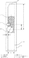
実施の形態1.
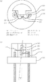
図1に本発明の実施の形態に係るワイヤボンド用の電極パターンの概略図を示す。また、図2に本発明の実施の形態に係るワイヤボンド用の電極パターンを用いた半導体素子の概略図を示す。以下、図1、図2を用いて説明する。本発明の実施の形態では細長いレーザダイオードチップにワイヤボンドを行った半導体素子を例とする。レーザダイオードチップには、ワイヤボンドのための電極パターン103が形成されている。この電極パターン103上のワイヤボンドを行う領域111内に直径dのAuボール109を形成してワイヤボンドを行う。その際、図2に示すアイレット201中心とレーザダイオード205の中心の傾きずれが無い状態(θ=0)のときには、中心が電極パターン103の短辺に平行な方向における中心を通る長辺方向の線上となるように、Auボール109を形成してワイヤボンドを行う。電極パターン103にはワイヤボンド認識パターン107となる特徴的なパターンが形成されている。本実施の形態では電極パターン103の長手方向の1辺に矩形の切り抜きを形成し、ワイヤボンド認識パターン107としている。各寸法を以下のように定める。
L:電極パターンのエッジ部(電極端部105)とワイヤボンド領域111に形成されたAuボール109の中心との最短距離(μm)
Lb:ワイヤボンド認識パターン107の長辺方向における中心を通る短辺に平行な方向の線とワイヤボンド領域111に形成されたAuボール109の中心との最短距離(μm)
d:Auボール109の直径(μm)
W:電極パターン103の短辺に平行な方向の幅(μm)
アイレット201中心とレーザダイオード205の中心の傾きずれ量θは組立て装置精度より最大2°となる。ワイヤボンド領域111にAuボール109を形成する際に、ワイヤボンド領域111からはみ出す量をxとすると、xは次式で表される。
x=d/2−W/2+Ltanθ(μm)
ここではみ出し量xをd/8まで許容した場合、tan2°=0.0349なので、LとLbはそれぞれ次式となる。
L=14.3×(W−3d/4)(μm)
Lb=14.3×(W−3d/4)(μm)
本実施の形態では、電極端部105をワイヤボンドの位置を特定するための基準となるワイヤボンド基準パターンとしている。このワイヤボンド基準パターンとワイヤボンド領域111内の直径dのAuボール109の中心との距離Lが、
L≧14.3×(W−3d/4)(μm)となる位置にワイヤボンドされる。このとき、電極パターン103上に形成されたワイヤボンド認識パターン107の長手方向における中心を通る短辺に平行な方向の線とAuボール109の中心との距離Lbは
Lb≦14.3×(W−3d/4)(μm)
となるように位置決めされる。記録型高出力レーザダイオードを例にすると、レーザダイオードの長手方向の長さを2000μm、幅120μm、電極の幅を80μmとして、Auボール径が80±10μmでは、Lは286μm程度となり、ワイヤボンド認識パターン無しでは、細長い電極の端の方にしかAuボールが形成できず、注入される電流密度が電極上端部と下端部で変わってしまい、レーザダイオードの動作が安定しない。本発明のワイヤボンド認識パターンを所望の位置に形成することにより、注入される電流密度の不均一を簡単に解消することができる。
本実施の形態では、ワイヤボンド基準パターンとして電極端部105を用いたが、電極端部以外にも、電極内の特徴的なパターンをワイヤボンド基準パターンとすることができる。例えば、電極パターン103の四隅のひとつには、チップの前後確認等のための切り欠きが形成されており、この切り欠きをワイヤボンド基準パターンとすることもできる。本実施の形態では、この切り欠きは矩形を組合わせた形状となっているが、円形や三角形など他の形状でも構わない。また、本実施の形態では、Auボール109を形成してワイヤボンドを行ったが、ウェッジボンドの場合にはAuボールを形成せず、ワイヤ先端を超音波圧着して結線する。
Embodiment 1 FIG.
FIG. 1 shows a schematic diagram of an electrode pattern for wire bonding according to an embodiment of the present invention. FIG. 2 shows a schematic diagram of a semiconductor element using the wire bond electrode pattern according to the embodiment of the present invention. Hereinafter, a description will be given with reference to FIGS. In the embodiment of the present invention, a semiconductor element in which wire bonding is performed on an elongated laser diode chip is taken as an example. An
L: shortest distance (μm) between the edge portion (electrode end portion 105) of the electrode pattern and the center of the
Lb: the shortest distance (μm) between the line in the direction parallel to the short side passing through the center in the long side direction of the wire
d: Diameter of the Au ball 109 (μm)
W: Width in the direction parallel to the short side of the electrode pattern 103 (μm)
The tilt deviation amount θ between the center of the
x = d / 2−W / 2 + Ltanθ (μm)
Here, when the protrusion amount x is allowed up to d / 8, tan2 ° = 0.0349, so L and Lb are respectively expressed by the following equations.
L = 14.3 × (W-3d / 4) (μm)
Lb = 14.3 × (W-3d / 4) (μm)
In the present embodiment, the electrode end portion 105 is a wire bond reference pattern that serves as a reference for specifying the position of the wire bond. The distance L between this wire bond reference pattern and the center of the
Wire bonding is performed at a position where L ≧ 14.3 × (W−3d / 4) (μm) . At this time, the distance Lb between the line in the direction parallel to the short side passing through the center in the longitudinal direction of the wire
Is positioned so that Taking a recordable high-power laser diode as an example, if the length in the longitudinal direction of the laser diode is 2000 μm, the width is 120 μm, the width of the electrode is 80 μm, the Au ball diameter is 80 ± 10 μm, L is about 286 μm, and wire bond recognition Without a pattern, an Au ball can be formed only at the end of the elongated electrode, and the injected current density changes at the upper end and lower end of the electrode, and the operation of the laser diode is not stable. By forming the wire bond recognition pattern of the present invention at a desired position, the nonuniformity of the injected current density can be easily eliminated.
In this embodiment, the electrode end portion 105 is used as the wire bond reference pattern. However, a characteristic pattern in the electrode can be used as the wire bond reference pattern in addition to the electrode end portion. For example, a notch for confirming the front and back of the chip is formed at one of the four corners of the
実施の形態2.
図3および図4に本発明の実施の形態2に係るワイヤボンド用の電極パターンの概略図を示す。実施の形態1では、図1に示すようにワイヤボンド認識パターン107を矩形の切り欠きパターンとしていたが、本実施の形態ではワイヤボンド認識パターンを図3に示すような丸い認識パターン形状、あるいは図4に示すような三角形状にした。円状のワイヤボンド認識パターン307では、このワイヤボンド認識パターン307を小さくした場合や、加工精度の低いエッチング法を用いた場合にエッチングだれが生じても、形状は丸い円状のまま変わらず、認識エラーを防ぐことができる。また、三角形状のワイヤボンド認識パターン407の場合は、同じ大きさの四角い形状に比べて直線部の長さを長くできるためにエッチングだれ等によるパターン崩れの影響を少なくすることができる効果がある。
ワイヤボンド認識パターン307、407は電極パターン303、403の長手方向の一辺の側部に形成することによりリフトオフ法で容易に形成することができる。また、エッチング等の方法を用いる場合には、図5に示すように、ワイヤボンド認識パターン507を電極パターン503の内部に形成してもよい。
Embodiment 2. FIG.
3 and 4 are schematic diagrams of electrode patterns for wire bonding according to Embodiment 2 of the present invention. In the first embodiment, the wire
The wire
実施の形態3.
本実施の形態は、ワイヤボンド認識パターンを認識しワイヤボンディングを行う方法に関するものである。
図1および図2を参照し、アイトレット201の外形を認識することでワイヤボンド認識パターン107のおおよその位置を知ることができる。次に、電極パターン103に形成されたワイヤボンド認識パターン107を認識する。このとき必要であればカメラ倍率を変更してワイヤボンド認識パターン107を認識する。最後にワイヤ211、213でワイヤボンドを行い、リード207、GNDへの結線を行う。この方法を用いた場合、アイレット201上のレーザダイオード205が、設定ミス、プリアライメントの不具合等や位置決め治具の不具合等で所定の位置からずれてしまったときにそれを即座に見つけることが可能となる。すなわちアイレット外形の認識後に予想位置にワイヤボンド認識パターンがないため、装置はそこで停止する。これはレーザダイオード接着工程での位置ずれ不良品の生産を最低限にできるため、不良品を作り続けることによるロスを抑える効果がある。
Embodiment 3 FIG.
The present embodiment relates to a method for recognizing a wire bond recognition pattern and performing wire bonding.
With reference to FIGS. 1 and 2, the approximate position of the wire
実施の形態4.
本実施の形態は、ワイヤボンド認識パターンを認識しワイヤボンディングを行う他の方法に関するものである。
実施の形態3と同様に、アイトレットの外形を認識することでワイヤボンド認識パターンのおおよその位置を知ることができる。次に、ワイヤボンドの基準となるワイヤボンド基準パターンを認識する。本実施の形態では、電極端部105をワイヤボンド基準パターンとして用いる。次に電極パターン103に形成されたワイヤボンド認識パターン107を認識する。このとき、必要であればカメラ倍率を変更してワイヤボンド認識パターン107を認識する。最後にワイヤボンドを行う。この方法を用いた場合、一旦チップの位置を確認するので、実施の形態3よりも正確にワイヤボンド認識パターン107の位置を認識することができる。また、電極パターン103の四隅のひとつに形成された切り欠きをワイヤボンド基準パターンとして位置確認に使用することもできる。本実施の形態では、この切り欠きは矩形を組合わせた形状となっているが、円形や三角形など他の形状でも構わない。
Embodiment 4 FIG.
The present embodiment relates to another method for recognizing a wire bond recognition pattern and performing wire bonding.
Similar to the third embodiment, it is possible to know the approximate position of the wire bond recognition pattern by recognizing the outer shape of the eyelet. Next, a wire bond reference pattern serving as a wire bond reference is recognized. In this embodiment, the electrode end portion 105 is used as a wire bond reference pattern. Next, the wire
実施の形態5.
本実施の形態は、ワイヤボンド認識パターンを認識しワイヤボンディングを行う他の方法に関するものである。
まず図1を参照し、アイトレットの外形を認識することでワイヤボンド認識パターン107のおおよその位置を知ることができる。次に、電極パターン103に形成されたワイヤボンド認識パターン107を認識する。このとき必要であればカメラ倍率を変更してワイヤボンド認識パターン107を認識する。次に予想される位置にある電極端部105のパターンを認識し、最後にワイヤボンドを行う。この方法を用いた場合、実施の形態3のように接着工程での位置ずれを検知できるのに加えて、異機種のレーザダイオードチップを接着してしまったときの不良をすぐに検知できる。レーザダイオードチップは出力できる光パワーにより、レーザダイオード長手方向の長さが異なるので、異機種のチップの場合、電極端部のパターンを認識できなくなり、装置は停止するため、異機種チップ搭載不良を作り続けることによるロスを抑える効果がある。また、電極パターン103の四隅のひとつに形成された切り欠きを電極端部の確認に使用することもできる。本実施の形態では、この切り欠きは矩形を組合わせた形状となっているが、円形や三角形など他の形状でも構わない。
The present embodiment relates to another method for recognizing a wire bond recognition pattern and performing wire bonding.
First, referring to FIG. 1, the approximate position of the wire
なお、本発明は、短辺と長辺を有する電極パターンに関するものであるが、アイレットの中心線に対するレーザダイオードの中心線の傾きずれによる影響は、電極パターンの短辺方向の幅Wが小さいほど大きい。Wが大きい場合には、ずれに対するマージンが大きくなるが、Wが100μm以下になるとこのマージンがほとんど無くなる。従って、本発明は、Wが100μm以下の場合に特に効果を有する。 Although the present invention relates to an electrode pattern having a short side and a long side, the influence of the tilt deviation of the center line of the laser diode with respect to the center line of the eyelet is smaller as the width W in the short side direction of the electrode pattern is smaller. large. When W is large, the margin for deviation becomes large, but when W is 100 μm or less, this margin is almost eliminated. Therefore, the present invention is particularly effective when W is 100 μm or less.
なお、本発明は、記録型高出力レーザダイオードについて説明してきたが、それ以外にも赤色レーザダイオードや青紫色レーザダイオード、通信用レーザダイオード、LED、その他の半導体装置、またはパッケージや基板上等の配線パターンなどのワイヤボンディングを行う電極パターンにも適応することができる。 Although the present invention has been described with respect to the recording type high-power laser diode, other than that, a red laser diode, a blue-violet laser diode, a communication laser diode, an LED, other semiconductor devices, a package, a substrate, etc. It can also be applied to an electrode pattern for wire bonding such as a wiring pattern.
103 電極パターン
105 電極端部
107 ワイヤボンド認識パターン
109 Auボール
303 電極パターン
307 ワイヤボンド認識パターン
403 電極パターン
407 ワイヤボンド認識パターン
503 電極パターン
507 ワイヤボンド認識パターン
DESCRIPTION OF
Claims (8)
ワイヤボンドの位置を決めるための基準位置を示すワイヤボンド基準パターンとワイヤボンド認識パターンを有し、
前記電極パターンに接着されたワイヤボンディング用の金属部位で前記短辺に平行な方向の幅が最大となる位置を通る前記短辺に平行な方向の線と前記基準位置との距離Lと、
前記ワイヤボンド認識パターンの前記長辺方向における中心を通る前記短辺に平行な方向の線と前記金属部位の前記短辺に平行な方向の幅が最大となる位置を通る前記短辺に平行な方向の線との距離Lbが
L≧14.3×(W−3d/4)(μm)
Lb≦14.3×(W−3d/4)(μm)
ただし、
d:電極パターンに接着されたワイヤボンディング用金属部位の前記短辺に平行な方向の幅の最大値(μm)
W:電極パターンの短辺に平行な方向の幅(μm)
であることを特徴とする電極パターン。 An electrode pattern for wire bonding having a short side and a long side,
A wire bond reference pattern indicating a reference position for determining the position of the wire bond and a wire bond recognition pattern;
A distance L between a line in a direction parallel to the short side and a reference position passing through a position where a width in a direction parallel to the short side is maximum in a metal part for wire bonding bonded to the electrode pattern;
The wire bond recognition pattern is parallel to the short side passing through the position where the line in the direction parallel to the short side passing through the center in the long side direction and the width of the metal part in the direction parallel to the short side is maximum. The distance Lb from the direction line is L ≧ 14.3 × (W-3d / 4) (μm)
Lb ≦ 14.3 × (W-3d / 4) (μm)
However,
d: Maximum width (μm) in the direction parallel to the short side of the wire bonding metal part bonded to the electrode pattern
W: Width in the direction parallel to the short side of the electrode pattern (μm)
The electrode pattern characterized by being.
Priority Applications (5)
| Application Number | Priority Date | Filing Date | Title |
|---|---|---|---|
| JP2008008066A JP5176557B2 (en) | 2007-03-19 | 2008-01-17 | Electrode pattern and wire bonding method |
| TW097107465A TWI387171B (en) | 2007-03-19 | 2008-03-04 | Electrode pattern and wire bonding method |
| KR1020080020362A KR100941106B1 (en) | 2007-03-19 | 2008-03-05 | Electrode pattern and wire bonding method |
| US12/042,650 US7550673B2 (en) | 2007-03-19 | 2008-03-05 | Electrode pattern and wire bonding method |
| CN2008100830350A CN101272034B (en) | 2007-03-19 | 2008-03-18 | Electrode pattern and wire bonding method |
Applications Claiming Priority (3)
| Application Number | Priority Date | Filing Date | Title |
|---|---|---|---|
| JP2007070684 | 2007-03-19 | ||
| JP2007070684 | 2007-03-19 | ||
| JP2008008066A JP5176557B2 (en) | 2007-03-19 | 2008-01-17 | Electrode pattern and wire bonding method |
Publications (3)
| Publication Number | Publication Date |
|---|---|
| JP2008263165A JP2008263165A (en) | 2008-10-30 |
| JP2008263165A5 JP2008263165A5 (en) | 2011-01-20 |
| JP5176557B2 true JP5176557B2 (en) | 2013-04-03 |
Family
ID=39985396
Family Applications (1)
| Application Number | Title | Priority Date | Filing Date |
|---|---|---|---|
| JP2008008066A Active JP5176557B2 (en) | 2007-03-19 | 2008-01-17 | Electrode pattern and wire bonding method |
Country Status (4)
| Country | Link |
|---|---|
| JP (1) | JP5176557B2 (en) |
| KR (1) | KR100941106B1 (en) |
| CN (1) | CN101272034B (en) |
| TW (1) | TWI387171B (en) |
Families Citing this family (2)
| Publication number | Priority date | Publication date | Assignee | Title |
|---|---|---|---|---|
| JP5441590B2 (en) * | 2009-09-29 | 2014-03-12 | 大王製紙株式会社 | Pants-type disposable diaper |
| JP6901902B2 (en) * | 2017-04-27 | 2021-07-14 | ルネサスエレクトロニクス株式会社 | Semiconductor devices and their manufacturing methods |
Family Cites Families (12)
| Publication number | Priority date | Publication date | Assignee | Title |
|---|---|---|---|---|
| JPS62291126A (en) | 1986-06-11 | 1987-12-17 | Fuji Xerox Co Ltd | Pattern recognition mark |
| JPS63133638A (en) * | 1986-11-26 | 1988-06-06 | Toshiba Corp | Wire bonding |
| JP2621420B2 (en) * | 1988-09-28 | 1997-06-18 | 日本電気株式会社 | Bonding pads for semiconductor devices |
| JP2992427B2 (en) * | 1993-07-16 | 1999-12-20 | 株式会社カイジョー | Wire bonding apparatus and method |
| JP3611948B2 (en) * | 1997-05-16 | 2005-01-19 | 日本テキサス・インスツルメンツ株式会社 | Semiconductor device and manufacturing method thereof |
| JP2982794B1 (en) | 1998-06-17 | 1999-11-29 | 日本電気株式会社 | Semiconductor device |
| JP2001024303A (en) | 1999-07-09 | 2001-01-26 | Nippon Avionics Co Ltd | Recognition mark |
| JP4352579B2 (en) * | 2000-05-16 | 2009-10-28 | 沖電気工業株式会社 | Semiconductor chip and manufacturing method thereof |
| US6789724B2 (en) * | 2001-07-06 | 2004-09-14 | Erico International Corporation | Welding apparatus and method |
| AU2003220938A1 (en) * | 2002-05-28 | 2003-12-12 | Hitachi Chemical Co., Ltd. | Substrate, wiring board, semiconductor package-use substrate, semiconductor package and production methods for them |
| US7042098B2 (en) | 2003-07-07 | 2006-05-09 | Freescale Semiconductor,Inc | Bonding pad for a packaged integrated circuit |
| JP2005183669A (en) * | 2003-12-19 | 2005-07-07 | Tdk Corp | Mounting substrate and electronic component using it |
-
2008
- 2008-01-17 JP JP2008008066A patent/JP5176557B2/en active Active
- 2008-03-04 TW TW097107465A patent/TWI387171B/en active
- 2008-03-05 KR KR1020080020362A patent/KR100941106B1/en active IP Right Grant
- 2008-03-18 CN CN2008100830350A patent/CN101272034B/en active Active
Also Published As
| Publication number | Publication date |
|---|---|
| TWI387171B (en) | 2013-02-21 |
| JP2008263165A (en) | 2008-10-30 |
| KR20080085687A (en) | 2008-09-24 |
| KR100941106B1 (en) | 2010-02-10 |
| CN101272034B (en) | 2010-09-29 |
| TW200843265A (en) | 2008-11-01 |
| CN101272034A (en) | 2008-09-24 |
Similar Documents
| Publication | Publication Date | Title |
|---|---|---|
| US7361983B2 (en) | Semiconductor device and semiconductor assembly module with a gap-controlling lead structure | |
| US8704342B2 (en) | Resin sealing type semiconductor device and method of manufacturing the same, and lead frame | |
| JP4768384B2 (en) | Optical transmission line holding member and optical module | |
| US9136225B2 (en) | Semiconductor device manufacturing method | |
| JP2008186891A (en) | Mold package and its manufacturing method, and mounting structure of the mold package | |
| JP5714157B1 (en) | Power semiconductor device | |
| JP5176557B2 (en) | Electrode pattern and wire bonding method | |
| GB2323474A (en) | A leadframe for a semiconductor device | |
| KR20180045842A (en) | Chip packaging structure and related inner lead bonding method | |
| US20100141250A1 (en) | Magnetic sensor module | |
| CN106469689B (en) | Electronic component and forming method thereof | |
| US7550673B2 (en) | Electrode pattern and wire bonding method | |
| JP2010040884A (en) | Semiconductor device and method of bonding semiconductor chip | |
| JP5217013B2 (en) | Power conversion device and manufacturing method thereof | |
| JP2007227724A (en) | Semiconductor light-emitting device | |
| KR102072527B1 (en) | Semiconductor device and manufacturing method thereof | |
| JP3469840B2 (en) | Semiconductor device | |
| JPH06252326A (en) | Multi-terminal component, wiring substrate and packaging structure of multi-terminal component | |
| JP2008147427A (en) | Electronic component device and electronic component mounting method | |
| US10020225B2 (en) | Method of manufacturing semiconductor device | |
| JP5572007B2 (en) | Electronic device and manufacturing method thereof | |
| JP2010003909A (en) | Method of manufacturing semiconductor device | |
| JP2012069563A (en) | Lead frame, method of manufacturing the same, and manufacturing apparatus | |
| JP6504019B2 (en) | Light emitting device | |
| JP4960519B2 (en) | Optical transmission line holding member and optical module |
Legal Events
| Date | Code | Title | Description |
|---|---|---|---|
| A521 | Request for written amendment filed |
Free format text: JAPANESE INTERMEDIATE CODE: A523 Effective date: 20101130 |
|
| A621 | Written request for application examination |
Free format text: JAPANESE INTERMEDIATE CODE: A621 Effective date: 20101130 |
|
| A977 | Report on retrieval |
Free format text: JAPANESE INTERMEDIATE CODE: A971007 Effective date: 20120328 |
|
| A131 | Notification of reasons for refusal |
Free format text: JAPANESE INTERMEDIATE CODE: A131 Effective date: 20121016 |
|
| A521 | Request for written amendment filed |
Free format text: JAPANESE INTERMEDIATE CODE: A523 Effective date: 20121122 |
|
| TRDD | Decision of grant or rejection written | ||
| A01 | Written decision to grant a patent or to grant a registration (utility model) |
Free format text: JAPANESE INTERMEDIATE CODE: A01 Effective date: 20121211 |
|
| A61 | First payment of annual fees (during grant procedure) |
Free format text: JAPANESE INTERMEDIATE CODE: A61 Effective date: 20121224 |
|
| R150 | Certificate of patent or registration of utility model |
Ref document number: 5176557 Country of ref document: JP Free format text: JAPANESE INTERMEDIATE CODE: R150 |
|
| R250 | Receipt of annual fees |
Free format text: JAPANESE INTERMEDIATE CODE: R250 |
|
| R250 | Receipt of annual fees |
Free format text: JAPANESE INTERMEDIATE CODE: R250 |
|
| R250 | Receipt of annual fees |
Free format text: JAPANESE INTERMEDIATE CODE: R250 |
|
| R250 | Receipt of annual fees |
Free format text: JAPANESE INTERMEDIATE CODE: R250 |
|
| R250 | Receipt of annual fees |
Free format text: JAPANESE INTERMEDIATE CODE: R250 |
|
| R250 | Receipt of annual fees |
Free format text: JAPANESE INTERMEDIATE CODE: R250 |
|
| R250 | Receipt of annual fees |
Free format text: JAPANESE INTERMEDIATE CODE: R250 |
|
| R250 | Receipt of annual fees |
Free format text: JAPANESE INTERMEDIATE CODE: R250 |
|
| R250 | Receipt of annual fees |
Free format text: JAPANESE INTERMEDIATE CODE: R250 |