JP5154951B2 - Semiconductor device and display device - Google Patents
Semiconductor device and display device Download PDFInfo
- Publication number
- JP5154951B2 JP5154951B2 JP2007553828A JP2007553828A JP5154951B2 JP 5154951 B2 JP5154951 B2 JP 5154951B2 JP 2007553828 A JP2007553828 A JP 2007553828A JP 2007553828 A JP2007553828 A JP 2007553828A JP 5154951 B2 JP5154951 B2 JP 5154951B2
- Authority
- JP
- Japan
- Prior art keywords
- insulating film
- layer
- circuit element
- semiconductor device
- film
- Prior art date
- Legal status (The legal status is an assumption and is not a legal conclusion. Google has not performed a legal analysis and makes no representation as to the accuracy of the status listed.)
- Expired - Fee Related
Links
Images


Classifications
-
- H—ELECTRICITY
- H10—SEMICONDUCTOR DEVICES; ELECTRIC SOLID-STATE DEVICES NOT OTHERWISE PROVIDED FOR
- H10D—INORGANIC ELECTRIC SEMICONDUCTOR DEVICES
- H10D30/00—Field-effect transistors [FET]
- H10D30/60—Insulated-gate field-effect transistors [IGFET]
- H10D30/67—Thin-film transistors [TFT]
- H10D30/6729—Thin-film transistors [TFT] characterised by the electrodes
- H10D30/673—Thin-film transistors [TFT] characterised by the electrodes characterised by the shapes, relative sizes or dispositions of the gate electrodes
-
- H—ELECTRICITY
- H10—SEMICONDUCTOR DEVICES; ELECTRIC SOLID-STATE DEVICES NOT OTHERWISE PROVIDED FOR
- H10D—INORGANIC ELECTRIC SEMICONDUCTOR DEVICES
- H10D30/00—Field-effect transistors [FET]
- H10D30/60—Insulated-gate field-effect transistors [IGFET]
- H10D30/67—Thin-film transistors [TFT]
- H10D30/6729—Thin-film transistors [TFT] characterised by the electrodes
- H10D30/6737—Thin-film transistors [TFT] characterised by the electrodes characterised by the electrode materials
- H10D30/6739—Conductor-insulator-semiconductor electrodes
-
- H—ELECTRICITY
- H10—SEMICONDUCTOR DEVICES; ELECTRIC SOLID-STATE DEVICES NOT OTHERWISE PROVIDED FOR
- H10D—INORGANIC ELECTRIC SEMICONDUCTOR DEVICES
- H10D86/00—Integrated devices formed in or on insulating or conducting substrates, e.g. formed in silicon-on-insulator [SOI] substrates or on stainless steel or glass substrates
- H10D86/40—Integrated devices formed in or on insulating or conducting substrates, e.g. formed in silicon-on-insulator [SOI] substrates or on stainless steel or glass substrates characterised by multiple TFTs
- H10D86/431—Integrated devices formed in or on insulating or conducting substrates, e.g. formed in silicon-on-insulator [SOI] substrates or on stainless steel or glass substrates characterised by multiple TFTs having different compositions, shapes, layouts or thicknesses of gate insulators in different TFTs
-
- H—ELECTRICITY
- H10—SEMICONDUCTOR DEVICES; ELECTRIC SOLID-STATE DEVICES NOT OTHERWISE PROVIDED FOR
- H10D—INORGANIC ELECTRIC SEMICONDUCTOR DEVICES
- H10D86/00—Integrated devices formed in or on insulating or conducting substrates, e.g. formed in silicon-on-insulator [SOI] substrates or on stainless steel or glass substrates
- H10D86/40—Integrated devices formed in or on insulating or conducting substrates, e.g. formed in silicon-on-insulator [SOI] substrates or on stainless steel or glass substrates characterised by multiple TFTs
- H10D86/60—Integrated devices formed in or on insulating or conducting substrates, e.g. formed in silicon-on-insulator [SOI] substrates or on stainless steel or glass substrates characterised by multiple TFTs wherein the TFTs are in active matrices
-
- H—ELECTRICITY
- H10—SEMICONDUCTOR DEVICES; ELECTRIC SOLID-STATE DEVICES NOT OTHERWISE PROVIDED FOR
- H10P—GENERIC PROCESSES OR APPARATUS FOR THE MANUFACTURE OR TREATMENT OF DEVICES COVERED BY CLASS H10
- H10P95/00—Generic processes or apparatus for manufacture or treatments not covered by the other groups of this subclass
- H10P95/94—Hydrogenation or deuterisation, e.g. using atomic hydrogen from a plasma
-
- G—PHYSICS
- G02—OPTICS
- G02F—OPTICAL DEVICES OR ARRANGEMENTS FOR THE CONTROL OF LIGHT BY MODIFICATION OF THE OPTICAL PROPERTIES OF THE MEDIA OF THE ELEMENTS INVOLVED THEREIN; NON-LINEAR OPTICS; FREQUENCY-CHANGING OF LIGHT; OPTICAL LOGIC ELEMENTS; OPTICAL ANALOGUE/DIGITAL CONVERTERS
- G02F1/00—Devices or arrangements for the control of the intensity, colour, phase, polarisation or direction of light arriving from an independent light source, e.g. switching, gating or modulating; Non-linear optics
- G02F1/01—Devices or arrangements for the control of the intensity, colour, phase, polarisation or direction of light arriving from an independent light source, e.g. switching, gating or modulating; Non-linear optics for the control of the intensity, phase, polarisation or colour
- G02F1/13—Devices or arrangements for the control of the intensity, colour, phase, polarisation or direction of light arriving from an independent light source, e.g. switching, gating or modulating; Non-linear optics for the control of the intensity, phase, polarisation or colour based on liquid crystals, e.g. single liquid crystal display cells
- G02F1/133—Constructional arrangements; Operation of liquid crystal cells; Circuit arrangements
- G02F1/136—Liquid crystal cells structurally associated with a semi-conducting layer or substrate, e.g. cells forming part of an integrated circuit
- G02F1/1362—Active matrix addressed cells
- G02F1/136286—Wiring, e.g. gate line, drain line
- G02F1/136295—Materials; Compositions; Manufacture processes
-
- H—ELECTRICITY
- H10—SEMICONDUCTOR DEVICES; ELECTRIC SOLID-STATE DEVICES NOT OTHERWISE PROVIDED FOR
- H10D—INORGANIC ELECTRIC SEMICONDUCTOR DEVICES
- H10D30/00—Field-effect transistors [FET]
- H10D30/60—Insulated-gate field-effect transistors [IGFET]
- H10D30/67—Thin-film transistors [TFT]
- H10D30/6704—Thin-film transistors [TFT] having supplementary regions or layers in the thin films or in the insulated bulk substrates for controlling properties of the device
- H10D30/6713—Thin-film transistors [TFT] having supplementary regions or layers in the thin films or in the insulated bulk substrates for controlling properties of the device characterised by the properties of the source or drain regions, e.g. compositions or sectional shapes
- H10D30/6715—Thin-film transistors [TFT] having supplementary regions or layers in the thin films or in the insulated bulk substrates for controlling properties of the device characterised by the properties of the source or drain regions, e.g. compositions or sectional shapes characterised by the doping profiles, e.g. having lightly-doped source or drain extensions
Landscapes
- Thin Film Transistor (AREA)
- Metal-Oxide And Bipolar Metal-Oxide Semiconductor Integrated Circuits (AREA)
Description
本発明は、半導体装置、その製造方法及び表示装置に関する。より詳しくは、アクティブマトリクス基板等の半導体装置、その製造方法及び表示装置に関するものである。 The present invention relates to a semiconductor device, a manufacturing method thereof, and a display device. More specifically, the present invention relates to a semiconductor device such as an active matrix substrate, a manufacturing method thereof, and a display device.
半導体装置は、半導体の電気特性を利用した能動素子を備えた電子装置であり、例えば、オーディオ機器、通信機器、コンピュータ、家電機器等に広く応用されている。中でも、基板上に薄膜トランジスタ(以下「TFT」ともいう。)を備える半導体装置として、TFTアレイ基板が知られており、アクティブマトリクス駆動方式の液晶表示装置等の構成部材として利用されている。 A semiconductor device is an electronic device that includes an active element that utilizes electrical characteristics of a semiconductor, and is widely applied to, for example, audio equipment, communication equipment, computers, and home appliances. Among them, a TFT array substrate is known as a semiconductor device including a thin film transistor (hereinafter also referred to as “TFT”) on a substrate, and is used as a constituent member of an active matrix liquid crystal display device or the like.
ところで、近年、アクティブマトリクス駆動方式の液晶表示装置では、TFTの半導体材料としてポリシリコン(以下「p−Si」ともいう。)を用いることにより、画素回路部と駆動回路部とを同一の基板上に設けるシステムオングラス技術が活用されつつある。この技術を活用すれば、画素回路部のTFT(以下「画素スイッチング用TFT」ともいう。)と駆動回路部のTFT(以下「駆動回路用TFT」ともいう。)とを一体的に形成することにより、液晶表示装置の小型化、低消費電力化及び高信頼性を実現することができる。しかしながら、画素スイッチング用TFTと駆動回路用TFTとでは、要求される特性が異なる。すなわち、画素スイッチング用TFTには、コントラスト比の低下やパネル内の画質の不均一を抑制するために低いオフ電流が要求されるのに対し、駆動回路用TFTには、駆動回路の高速動作を実現するために低閾値電圧(Vth)化、Vthバラツキ低減や高いオン電流が要求される。したがって、これらの要求特性を満たすべく、画素スイッチング用TFTと駆動回路用TFTとの間で、構造上の差異を設ける等の必要がある。 Incidentally, in recent years, in an active matrix liquid crystal display device, a pixel circuit portion and a drive circuit portion are formed on the same substrate by using polysilicon (hereinafter also referred to as “p-Si”) as a semiconductor material of a TFT. The system-on-glass technology provided in is being utilized. By utilizing this technology, the TFT of the pixel circuit portion (hereinafter also referred to as “pixel switching TFT”) and the TFT of the drive circuit portion (hereinafter also referred to as “driving circuit TFT”) are integrally formed. Accordingly, the liquid crystal display device can be reduced in size, reduced in power consumption, and high in reliability. However, the required characteristics are different between the pixel switching TFT and the driving circuit TFT. In other words, the pixel switching TFT is required to have a low off-current in order to suppress a decrease in contrast ratio and non-uniform image quality in the panel, while the driving circuit TFT has a high speed operation of the driving circuit. In order to achieve this, a low threshold voltage (Vth), Vth variation reduction, and a high on-current are required. Therefore, in order to satisfy these required characteristics, it is necessary to provide a structural difference between the pixel switching TFT and the driving circuit TFT.
このような方法としては、例えば、画素スイッチング用TFTのゲート絶縁膜の膜厚を駆動回路用TFTのゲート絶縁膜の膜厚よりも大きくする方法が知られている。例えば、半導体層とゲート電極との間に2層構造のゲート絶縁膜を有するマトリクス回路部TFT(画素スイッチング用TFT)と、1層構造のゲート絶縁膜を有する周辺回路部TFT(駆動回路用TFT)とが同一の基板上に形成された薄膜半導体装置が開示されている(例えば、特許文献1参照。)。この薄膜半導体装置においては、周辺回路部TFTのゲート絶縁膜は、酸化シリコン又は窒化シリコンからなる単層構造を有し、マトリクス回路部TFTのゲート絶縁膜は、下層部が周辺回路部TFTのゲート絶縁膜と同一の構造を有し、上層部が酸化シリコン又は窒化シリコンからなる単層構造を有する。しかしながら、この構成によれば、マトリクス回路部TFTにおいて、ゲート絶縁膜の上層部及び下層部の2層を連続成膜することが不可能であり、該上層部と下層部との界面にはトラップが多く存在するため、ゲート絶縁膜の下層部が酸化シリコンからなる単層構造を有する場合には、マトリクス回路部TFTの信頼性が低下してしまうという点で改善の余地があった。また、ゲート絶縁膜の上層部は、スパッタ又はプラズマCVD法により形成されるため、ゲート絶縁膜の下層部は、酸化シリコンからなる単層構造を有する場合に、ゲート絶縁膜の上層部の形成工程においてプラズマ損傷を受ける結果、マトリクス回路部TFTの信頼性がより低下してしまうという点で改善の余地があった。一方、マトリクス回路部TFTにおいて、ゲート絶縁膜の下層部が窒化シリコンからなる場合には、ゲート絶縁膜と半導体層(ポリシリコン層)との間で良質な界面を形成することができないため、良好なTFT特性を得ることができないという点で改善の余地があった。 As such a method, for example, a method is known in which the thickness of the gate insulating film of the pixel switching TFT is made larger than the thickness of the gate insulating film of the driving circuit TFT. For example, a matrix circuit portion TFT (pixel switching TFT) having a two-layer gate insulating film between a semiconductor layer and a gate electrode, and a peripheral circuit portion TFT (driving circuit TFT) having a one-layer gate insulating film ) Is formed on the same substrate (for example, see Patent Document 1). In this thin film semiconductor device, the gate insulating film of the peripheral circuit portion TFT has a single layer structure made of silicon oxide or silicon nitride, and the gate insulating film of the matrix circuit portion TFT has a lower layer portion of the gate of the peripheral circuit portion TFT. It has the same structure as the insulating film, and the upper layer portion has a single layer structure made of silicon oxide or silicon nitride. However, according to this configuration, in the matrix circuit portion TFT, it is impossible to continuously form the upper layer portion and the lower layer portion of the gate insulating film, and a trap is formed at the interface between the upper layer portion and the lower layer portion. Therefore, when the lower layer portion of the gate insulating film has a single layer structure made of silicon oxide, there is room for improvement in that the reliability of the matrix circuit portion TFT is lowered. In addition, since the upper layer portion of the gate insulating film is formed by sputtering or plasma CVD, when the lower layer portion of the gate insulating film has a single layer structure made of silicon oxide, the step of forming the upper layer portion of the gate insulating film As a result of the plasma damage, there is room for improvement in that the reliability of the matrix circuit TFT is further lowered. On the other hand, in the matrix circuit portion TFT, when the lower layer portion of the gate insulating film is made of silicon nitride, a good interface cannot be formed between the gate insulating film and the semiconductor layer (polysilicon layer). There was room for improvement in that it was not possible to obtain excellent TFT characteristics.
また、ゲート絶縁膜を構成する絶縁膜を形成した後、該絶縁膜の所定の領域をエッチングで選択的に除去することでゲート絶縁膜の厚さが異なる第1及び第2の電界効果型トランジスタを形成する半導体装置の製造方法が開示されている(例えば、特許文献2参照。)。しかしながら、この製造方法によれば、エッチングされる絶縁膜が単層構造を有するため、上記エッチングをドライエッチングで行った場合に、エッチングで除去して形成された部分がプラズマダメージを受けるため、信頼性を低下させてしまうことがあるという点で改善の余地があった。 In addition, after forming an insulating film constituting the gate insulating film, the first and second field effect transistors in which the thickness of the gate insulating film is different by selectively removing a predetermined region of the insulating film by etching. A method of manufacturing a semiconductor device that forms the substrate is disclosed (for example, see Patent Document 2). However, according to this manufacturing method, since the insulating film to be etched has a single layer structure, when the above etching is performed by dry etching, the portion formed by etching is subjected to plasma damage. There is room for improvement in that it may reduce the performance.
したがって、従来の製造方法では、画素スイッチング用TFT及び駆動回路用TFTを同一の基板上に作製する場合、いずれかのTFTがゲート絶縁膜に劣化やダメージを受けてしまい、信頼性が低くなるため、現在も量産化できていない。
本発明は、上記現状に鑑みてなされたものであり、高性能化を図ることができる回路素子と高耐圧化を図ることができる回路素子とを同一の基板上に有し、かつ高信頼性化を図ることができる半導体装置及び表示装置を提供することを目的とするものである。 The present invention has been made in view of the above situation, and has a circuit element capable of achieving high performance and a circuit element capable of achieving high breakdown voltage on the same substrate, and has high reliability. An object of the present invention is to provide a semiconductor device and a display device that can be realized.
本発明者は、第1半導体層、第1ゲート絶縁膜(第1絶縁膜)、第1ゲート電極(第1導電層)及び第3絶縁膜がこの順に積層された構造を有する第1薄膜トランジスタ(第1回路素子)と、第2半導体層、第1ゲート絶縁膜よりも膜厚が大きい第2ゲート絶縁膜(第2絶縁膜)及び第2ゲート電極(第2導電層)がこの順に積層された構造を有する第2薄膜トランジスタ(第2回路素子)とを基板上に有する半導体装置の製造方法について種々検討したところ、上記第1ゲート絶縁膜及び第2ゲート絶縁膜を形成する方法に着目した。 The inventor has a first thin film transistor having a structure in which a first semiconductor layer, a first gate insulating film (first insulating film), a first gate electrode (first conductive layer), and a third insulating film are stacked in this order. A first circuit element), a second semiconductor layer, a second gate insulating film (second insulating film) having a thickness larger than the first gate insulating film, and a second gate electrode (second conductive layer) are laminated in this order. As a result of various studies on a method of manufacturing a semiconductor device having a second thin film transistor (second circuit element) having the above structure on a substrate, attention was focused on the method of forming the first gate insulating film and the second gate insulating film.
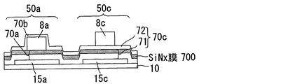
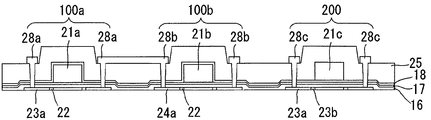
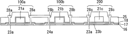
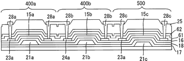
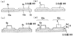
そして、例えば、図18(a)〜(d)に示すように、第1半導体層15a及び第2半導体層15c上に、酸化シリコン(SiO2)からなる第1ゲート絶縁膜4a、及び、第2ゲート絶縁膜9の下層部4cを形成する工程(図18(a))と、第1ゲート電極5を形成する工程(図18(b))と、窒化シリコン(SiNx)等からなる第3絶縁膜(第3絶縁膜の一部すなわち下層部、中層部又は上層部であってもよい。)6a及び第2ゲート絶縁膜9の上層部6cを形成する工程(図18(c))と、第2ゲート電極8を形成する工程(図18(d))とをこの順に含む方法について検討した。この方法によれば、第1絶縁膜4aと第2ゲート絶縁膜9の下層部4cとを共通の工程で形成することができ、第3絶縁膜6aと第2ゲート絶縁膜9の下層部6cとを共通の工程で形成することができることから、図18(d)に示すように、SiO2の単層からなる第1ゲート絶縁膜4aと、SiO2からなる下層部4c及びSiNx等からなる上層部6cの2層構造を有する第2ゲート絶縁膜9とを簡便に形成することができる。Then, for example, as shown in FIGS. 18A to 18D, the first gate
しかしながら、この方法によれば、図18(b)に示す工程において、第1ゲート電極5は、通常、微細化を実現する観点から、金属膜等をドライエッチングすることで形成される。したがって、この工程において、プラズマに弱いSiO2からなる第1ゲート絶縁膜4a、及び、第2ゲート絶縁膜9の下層部4cは、プラズマに曝されて損傷を受けるため、第1TFT50a及び第2TFT50cの信頼性が低下してしまうことを見いだした。また、図18(c)に示す工程において、SiNx等からなる第3絶縁膜6a及び第2ゲート絶縁膜9の上層部6cは通常、膜厚均一性及び段差被覆性等の観点から、プラズマ化学的気相成長(CVD)法を用いて形成される。したがって、この工程においても、第2ゲート絶縁膜9の下層部4cはプラズマ損傷を受け、信頼性が低下してしまうことを見いだした。However, according to this method, in the step shown in FIG. 18B, the
更に、図18(a)〜(c)に示すように、第1TFT50aにおける第1ゲート絶縁膜4aと第3絶縁膜6aとは工程を分離して形成され、第2TFT50cにおける第2ゲート絶縁膜9の下層部4cと上層部6cとは工程を分離して形成される。したがって、第1ゲート絶縁膜4aと第3絶縁膜6aとの界面、及び、第2ゲート絶縁膜9の下層部4cと上層部6cとの界面には、ホウ素(B)、ナトリウム(Na)、リン(P)、重金属等の可動イオン(不純物)が付着している。この不純物は、後の工程でアニール等されることにより、第1ゲート絶縁膜4a、及び、第2ゲート絶縁膜9の下層部4c内ひいては第1半導体層15a及び第2半導体層15c内に拡散するため、第1TFT50a及び第2TFT50cの信頼性が更に低下してしまうことを見いだした。
Further, as shown in FIGS. 18A to 18C, the first
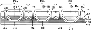
そこで、本発明者は、第1ゲート絶縁膜4a、及び、第2ゲート絶縁膜9の下層部4cの構造に着目した。そして、SiNxが高いプラズマ耐性を有することを見いだし、図19(a)〜(c)に示すような方法について検討した。そして、図19(a)に示すように、第1ゲート絶縁膜4a、及び、第2ゲート絶縁膜9の下層部4cの構造を最上層がSiNxからなる積層構造とすることにより、図19(b)及び(c)に示す工程において、第1ゲート絶縁膜4a、及び、第2ゲート絶縁膜9の下層部4cをプラズマ損傷から守ることができることを見いだした。Therefore, the inventor has focused on the structure of the
また、SiNxは不純物の拡散を防止(バリア)する機能も有することから、第1ゲート絶縁膜4a、及び、第2ゲート絶縁膜9の下層部4c上に付着した不純物は膜表面で捕獲(トラップ)されることにより、後のアニール工程等において、不純物が第1ゲート絶縁膜4a、及び、第2ゲート絶縁膜9の下層部4c内ひいては第1半導体層15a及び第2半導体層15c内に拡散することを抑制することができ、第1TFT50a及び第2TFT50cの信頼性の低下を抑制することができることを見いだした。更に、第1ゲート絶縁膜4a、及び、第2ゲート絶縁膜9の下層部4cの構造を積層構造とすることにより、第1ゲート絶縁膜4aの最下層7a、及び、第2ゲート絶縁膜9の下層部4cの最下層7cを構成する材料として、SiNxとは別に、第1半導体層15a及び第2半導体層15cと良質な界面を形成する材料(例えば、SiO2等。)を選択することができるため、第1TFT50a及び第2TFT50cの良好な特性を確保することができることを見いだした。Further, since SiN x also has a function of preventing (barriering) diffusion of impurities, impurities adhering to the
以上により、第1TFT50a及び第2TFT50cの信頼性を確保しつつ、第1TFT50aの高性能化及び第2TFT50cの高耐圧化を図ることができる結果、これらのTFTを同一の基板上に有する半導体装置の量産化を図ることができることを見いだした。また、本発明は、トップゲート構造のTFTのみならず、ボトムゲート構造、デュアルゲート構造のTFT、及び、保持容量素子等の回路素子を2以上基板上に有する半導体装置全般に適用することができることを見いだし、上記課題をみごとに解決することができることに想到し、本発明に到達したものである。
As described above, the reliability of the
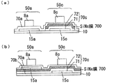
すなわち、本発明は、第1半導体層、第1絶縁膜、第1導電層及び第3絶縁膜がこの順に積層された構造を有する第1回路素子と、第2半導体層、第1絶縁膜よりも膜厚が大きい第2絶縁膜及び第2導電層がこの順に積層された構造を有する第2回路素子とを基板上に有する半導体装置であって、上記第1絶縁膜は、最上層が窒化シリコンからなる積層構造を有し、上記第2絶縁膜は、第1絶縁膜の積層構造を有する下層部と、第1導電層上の第3絶縁膜の構造を含む上層部とから構成される半導体装置(以下「第1半導体装置」ともいう。)である(例えば、図1参照。)。 That is, the present invention includes a first circuit element having a structure in which a first semiconductor layer, a first insulating film, a first conductive layer, and a third insulating film are stacked in this order, a second semiconductor layer, and a first insulating film. And a second circuit element having a structure in which a second insulating film and a second conductive layer having a large thickness are stacked in this order on a substrate, wherein the first insulating film is nitrided on the top layer The second insulating film has a laminated structure made of silicon, and the second insulating film includes a lower layer part having a laminated structure of the first insulating film and an upper layer part including a structure of the third insulating film on the first conductive layer. It is a semiconductor device (hereinafter also referred to as “first semiconductor device”) (for example, see FIG. 1).
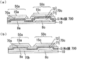
本発明はまた、第1半導体層、第1絶縁膜及び第1導電層がこの順に積層された構造を有する第1回路素子と、第2半導体層、第1絶縁膜よりも膜厚が大きい第2絶縁膜及び第2導電層がこの順に積層された構造を有する第2回路素子とを基板上に有する半導体装置であって、上記第2絶縁膜は、最上層が窒化シリコンからなる下層部と、第1絶縁膜の構造を有する上層部とから構成される半導体装置(以下「第2半導体装置」ともいう。)でもある(例えば、図2(a)参照。)。 The present invention also provides a first circuit element having a structure in which a first semiconductor layer, a first insulating film, and a first conductive layer are stacked in this order, and a second semiconductor layer having a thickness greater than that of the second semiconductor layer and the first insulating film. A semiconductor device having a second circuit element having a structure in which two insulating films and a second conductive layer are stacked in this order on a substrate, wherein the second insulating film includes a lower layer portion whose uppermost layer is made of silicon nitride, It is also a semiconductor device (hereinafter also referred to as “second semiconductor device”) composed of an upper layer portion having the structure of the first insulating film (see, for example, FIG. 2A).
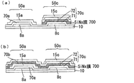
本発明は更に、第1導電層、第1絶縁膜及び第1半導体層がこの順に積層された構造を有する第1回路素子と、第2導電層、第1絶縁膜よりも膜厚が大きい第2絶縁膜、及び、第2半導体層がこの順に積層された構造を有する第2回路素子とを基板上に有する半導体装置であって、上記第1絶縁膜は、最下層が窒化シリコンからなる構造を有し、上記第2絶縁膜は、下層部と、第1絶縁膜の構造を有する上層部とから構成される半導体装置(以下「第3半導体装置」ともいう。)でもある(例えば、図3(a)参照。)。 The present invention further includes a first circuit element having a structure in which a first conductive layer, a first insulating film, and a first semiconductor layer are stacked in this order, a second conductive layer, and a second film having a thickness larger than that of the first conductive layer. 2. A semiconductor device having a second circuit element having a structure in which two insulating films and a second semiconductor layer are stacked in this order on a substrate, wherein the first insulating film has a structure in which a lowermost layer is made of silicon nitride The second insulating film is also a semiconductor device (hereinafter also referred to as “third semiconductor device”) including a lower layer portion and an upper layer portion having the structure of the first insulating film (for example, FIG. 3 (a).)
本発明はそして、第1導電層、第1絶縁膜及び第1半導体層がこの順に積層された構造を有する第1回路素子と、第2導電層、第1絶縁膜よりも膜厚が大きい第2絶縁膜、及び、第2半導体層がこの順に積層された構造を有する第2回路素子とを基板上に有する半導体装置であって、上記第2絶縁膜は、第1絶縁膜の構造を有する下層部と、最下層が窒化シリコンからなる上層部とから構成される半導体装置(以下「第4半導体装置」ともいう。)でもある(例えば、図4(a)参照。)。 According to the present invention, a first circuit element having a structure in which a first conductive layer, a first insulating film, and a first semiconductor layer are stacked in this order, a second conductive layer, a first film having a thickness larger than that of the first insulating film. 2. A semiconductor device having a second insulating film and a second circuit element having a structure in which a second semiconductor layer is laminated in this order on a substrate, wherein the second insulating film has a structure of a first insulating film. It is also a semiconductor device (hereinafter also referred to as “fourth semiconductor device”) composed of a lower layer portion and an upper layer portion whose bottom layer is made of silicon nitride (see, for example, FIG. 4A).
まず、本発明の第1半導体装置について詳述する。
本発明の第1半導体装置は、第1半導体層、第1絶縁膜、第1導電層及び第3絶縁膜がこの順に積層された構造を有する第1回路素子と、第2半導体層、第1絶縁膜よりも膜厚が大きい第2絶縁膜及び第2導電層がこの順に積層された構造を有する第2回路素子とを基板上に有するものである。上記第1半導体装置の好適な形態としては、例えば、(1)第1回路素子及び第2回路素子が薄膜トランジスタ(TFT)である形態、(2)第1回路素子がTFTであり、第2回路素子が保持容量素子である形態が挙げられる。(1)の場合、第1回路素子を第1TFTとし、第2回路素子を第2TFTとすると、第1TFTのゲート絶縁膜(第1絶縁膜)は、第2TFTのゲート絶縁膜(第2絶縁膜)よりも膜厚が小さいことから、第1回路素子は、第2回路素子よりも高速な動作を実現することができる高性能なTFTとして機能することができ、第2回路素子は、第1回路素子よりも絶縁破壊電圧が大きい高耐圧なTFTとして機能することができる。また、(2)の場合、第1回路素子を第3TFTとし、第2回路素子を保持容量素子とすると、第1絶縁膜(第3TFTのゲート絶縁膜)は、第2絶縁膜(保持容量素子の絶縁膜)よりも膜厚が小さいことから、第1回路素子は、高速な動作を実現することができる高性能なTFTとして機能することができ、第2回路素子は、絶縁破壊電圧が大きい高耐圧な保持容量素子として機能することができる。
なお、上記第1半導体装置内のTFTとしては、 トップゲート構造のTFT、デュアルゲート構造のTFT等が挙げられ、微細化の観点からは、トップゲート構造のTFTが好適である。First, the first semiconductor device of the present invention will be described in detail.
The first semiconductor device of the present invention includes a first circuit element having a structure in which a first semiconductor layer, a first insulating film, a first conductive layer, and a third insulating film are stacked in this order, a second semiconductor layer, The substrate has a second circuit element having a structure in which a second insulating film and a second conductive layer having a thickness larger than that of the insulating film are stacked in this order. As a suitable form of the first semiconductor device, for example, (1) a form in which the first circuit element and the second circuit element are thin film transistors (TFT), (2) a first circuit element is a TFT, and a second circuit There is a form in which the element is a storage capacitor element. In the case of (1), when the first circuit element is the first TFT and the second circuit element is the second TFT, the gate insulating film (first insulating film) of the first TFT is the gate insulating film (second insulating film) of the second TFT. ), The first circuit element can function as a high-performance TFT capable of realizing higher-speed operation than the second circuit element. It can function as a high breakdown voltage TFT having a higher breakdown voltage than a circuit element. In the case of (2), when the first circuit element is the third TFT and the second circuit element is the storage capacitor element, the first insulating film (gate insulating film of the third TFT) is the second insulating film (storage capacitor element). The first circuit element can function as a high-performance TFT capable of realizing high-speed operation, and the second circuit element has a high dielectric breakdown voltage. It can function as a high withstand voltage storage capacitor element.
Examples of the TFT in the first semiconductor device include a top gate TFT, a dual gate TFT, and the like. From the viewpoint of miniaturization, a top gate TFT is preferable.
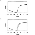
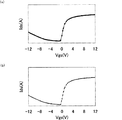
上記第1絶縁膜は、最上層が窒化シリコン(SiNx)からなる積層構造を有する(例えば、図1参照。)。SiNxは高いプラズマ耐性を有することから、上記第1絶縁膜がSiNx層を最上層として有することにより、第1絶縁膜にプラズマ損傷を与えることなく、第1導電層をプラズマエッチング(プラズマアッシング)等のドライエッチングで形成することができる。すなわち、第1絶縁膜の信頼性を保持しつつ、第1導電層ひいては第1回路素子の微細化を図ることができる。また、SiNxは不純物の拡散を防止する機能も有することから、第1絶縁膜のSiNx層上に付着したホウ素(B)、ナトリウム(Na)、リン(P)、重金属等の可動イオン(不純物)はそのままSiNx層の表面で捕獲(トラップ)される結果、不純物が第1絶縁膜ひいては第1半導体層内に拡散することを抑制することができる。したがって、第1回路素子(TFT等)の特性が変動(シフト)し、信頼性が低下するのを抑制することができる。更に、上記第1絶縁膜が積層構造を有することにより、上記第1絶縁膜の最下層を構成する材料を、最上層を構成する材料(SiNx)とは別個独立に選択することができる。すなわち、上記第1絶縁膜の最下層を構成する材料として、第1半導体層と良質な界面を形成する材料(例えば、SiO2等。)を選択することにより、第1回路素子について良好なドレイン電圧(Id)対ゲート電圧(Vg)特性(トランスファ特性)等を確保することができる。更に、上記第1絶縁膜が最上層としてSiNx層を有することから、第1導電層上に層間絶縁膜(SiNx膜)が設けられた場合に、層間絶縁膜の応力によってプラズマ損傷に似た損傷を受けることを低減することができる。そして、上記第1絶縁膜が誘電率の高いSiNxからなる層を有することにより、実効酸化膜厚(Equivalent Oxide Thickness:EOT)を低減することができるため、第1回路素子の更なる高性能化を図ることができる。The first insulating film has a stacked structure in which the uppermost layer is made of silicon nitride (SiN x ) (see, for example, FIG. 1). Since SiN x has high plasma resistance, the first insulating film has the SiN x layer as the uppermost layer, so that the first conductive layer is plasma-etched (plasma ashing) without causing plasma damage to the first insulating film. ) And the like can be formed by dry etching. In other words, the first conductive layer and thus the first circuit element can be miniaturized while maintaining the reliability of the first insulating film. Since SiN x also has a function of preventing the diffusion of impurities, mobile ions (such as boron (B), sodium (Na), phosphorus (P), and heavy metal) attached on the SiN x layer of the first insulating film ( As a result of trapping (impurities) as they are on the surface of the SiN x layer, it is possible to prevent the impurities from diffusing into the first insulating film and thus into the first semiconductor layer. Therefore, the characteristics of the first circuit element (TFT or the like) can be prevented from changing (shifting) and the reliability being lowered. Furthermore, since the first insulating film has a laminated structure, the material constituting the lowermost layer of the first insulating film can be selected independently of the material (SiN x ) constituting the uppermost layer. That is, by selecting a material (for example, SiO 2 or the like) that forms a good interface with the first semiconductor layer as a material constituting the lowermost layer of the first insulating film, an excellent drain for the first circuit element. A voltage (I d ) vs. gate voltage (V g ) characteristic (transfer characteristic) and the like can be ensured. Further, since the first insulating film has the SiN x layer as the uppermost layer, when an interlayer insulating film (SiN x film) is provided on the first conductive layer, it resembles plasma damage due to the stress of the interlayer insulating film. Damage can be reduced. Since the first insulating film has a layer made of SiN x having a high dielectric constant, an effective oxide thickness (EOT) can be reduced, so that further high performance of the first circuit element can be achieved. Can be achieved.
上記第2絶縁膜は、第1絶縁膜の積層構造を有する下層部と、第1導電層上の第3絶縁膜の構造を含む上層部とから構成される(例えば、図1参照。)。上記第2絶縁膜の下層部は、第1絶縁膜の積層構造と積層の数及び順序が同一の構造、すなわち最上層がSiNxからなる積層構造を有することから、第2絶縁膜の下層部にプラズマ損傷を与えることなく、第1導電層をプラズマエッチング等のドライエッチングで形成することができ、第2絶縁膜の上層部をプラズマCVD法等で形成することができる。したがって、第2絶縁膜の信頼性を保持しつつ、第1導電層ひいては第1回路素子の微細化を図ることができる。また、上記第2絶縁膜の下層部が積層構造を有することにより、上記第2絶縁膜の最下層を構成する材料を、該下層部の最上層を構成する材料(SiNx)とは別個独立に選択することができる。すなわち、上記第2絶縁膜の最下層を構成する材料として、第2半導体層と良質な界面を形成する材料(例えば、SiO2等。)を選択することにより、第2回路素子について良好なトランスファ特性等を確保することができる。更に、上記第2絶縁膜の下層部と上層部とは別々の工程で形成されるが、該下層部の最上層を構成するSiNxは不純物の拡散を防止する機能を有することから、第2絶縁膜の下層部上に付着した可動イオン(不純物)はそのままSiNx層の表面で捕獲(トラップ)される結果、不純物が第2絶縁膜の下層部内ひいては第2半導体層に拡散することを抑制することができる。したがって、第2TFTの特性が変動(シフト)し、信頼性が低下するのを抑制することができる。そして、上記第2絶縁膜の下層部が誘電率の高いSiNxからなる層を有することにより、第2絶縁膜の物理的な膜厚を増加させることができるため、第2回路素子の更なる高耐圧化を図ることができる。更には、上記第2絶縁膜の上層部が第1導電層上の第3絶縁膜の構造を含むことから、上記第2絶縁膜の上層部の形成する際のパターニング工程等の削減を図ることにより、製造工程の簡略化を図ることができる。
したがって、本発明の第1半導体装置によれば、信頼性を充分に確保しつつ、高性能化を図ることができる回路素子と高耐圧化を図ることができる回路素子とを同一の基板上に有する半導体装置の量産化を図ることができる。The second insulating film includes a lower layer portion having a laminated structure of the first insulating film and an upper layer portion including a structure of a third insulating film on the first conductive layer (see, for example, FIG. 1). Since the lower layer portion of the second insulating film has the same structure and the same number and order of lamination as the first insulating film, that is, the uppermost layer has a laminated structure made of SiN x , the lower layer portion of the second insulating film The first conductive layer can be formed by dry etching such as plasma etching without causing plasma damage, and the upper layer portion of the second insulating film can be formed by plasma CVD or the like. Therefore, the first conductive layer and thus the first circuit element can be miniaturized while maintaining the reliability of the second insulating film. Further, since the lower layer portion of the second insulating film has a laminated structure, the material constituting the lowermost layer of the second insulating film is made independent of the material (SiN x ) constituting the uppermost layer of the lower layer portion. Can be selected. That is, by selecting a material (for example, SiO 2 or the like) that forms a good interface with the second semiconductor layer as a material constituting the lowermost layer of the second insulating film, an excellent transfer can be achieved for the second circuit element. Characteristics and the like can be ensured. Furthermore, although the lower layer portion and the upper layer portion of the second insulating film are formed in separate steps, SiN x constituting the uppermost layer of the lower layer portion has a function of preventing the diffusion of impurities. Movable ions (impurities) adhering to the lower layer of the insulating film are trapped (trapped) as they are on the surface of the SiN x layer, thereby suppressing the diffusion of impurities into the lower layer of the second insulating film and thus to the second semiconductor layer. can do. Therefore, it is possible to prevent the characteristics of the second TFT from changing (shifting) and reducing reliability. Since the lower layer portion of the second insulating film has a layer made of SiN x having a high dielectric constant, the physical thickness of the second insulating film can be increased. High breakdown voltage can be achieved. Furthermore, since the upper layer portion of the second insulating film includes the structure of the third insulating film on the first conductive layer, the number of patterning steps when forming the upper layer portion of the second insulating film is reduced. As a result, the manufacturing process can be simplified.
Therefore, according to the first semiconductor device of the present invention, the circuit element capable of achieving high performance and the circuit element capable of achieving high breakdown voltage are provided on the same substrate while sufficiently ensuring reliability. The mass production of the semiconductor device can be achieved.
上記第1絶縁膜、及び、第2絶縁膜の下層部の構造は、積層構造すなわち2以上の層からなる構造である限り、例えば3以上の層からなる構造であってもよい。上記第1絶縁膜及び第2絶縁膜中のSiNx層以外の層を構成する材料としては特に限定されず、酸化シリコン(SiO2)、SiO2よりも誘電率が低い材料としてSiOF、SiOC等、SiO2よりも誘電率が高い材料として、二酸化チタン(TiO2)、三酸化二アルミニウム(Al2O3)、五酸化二タンタル(Ta2O5)等の酸化タンタル、二酸化ハフニウム(HfO2)、二酸化ジルコニウム(ZrO2)等が挙げられる。上記第1絶縁膜と第2絶縁膜の下層部とは、同一の工程で形成された(一体化された)層を含んでいてもよく、第1絶縁膜を構成する全ての層が、第2絶縁膜の下層部を構成する層とそれぞれ同一の工程で形成されたものであることが好ましい。The structure of the lower layer portion of the first insulating film and the second insulating film may be, for example, a structure composed of three or more layers as long as it is a laminated structure, that is, a structure composed of two or more layers. The material constituting the layers other than the SiN x layer in the first insulating film and the second insulating film is not particularly limited, and examples of the material having a dielectric constant lower than that of silicon oxide (SiO 2 ) and SiO 2 include SiOF and SiOC. as a material having a higher dielectric constant than SiO 2, titanium dioxide (TiO 2), dialuminum trioxide (Al 2 O 3), tantalum pentoxide (Ta 2 O 5) oxidation, such as tantalum, hafnium dioxide (HfO 2 ), Zirconium dioxide (ZrO 2 ) and the like. The first insulating film and the lower layer portion of the second insulating film may include a layer formed (integrated) in the same process, and all layers constituting the first insulating film It is preferable that each layer is formed in the same process as the layer constituting the lower layer portion of the insulating film.
これに対し、上記第3絶縁膜、及び、第2絶縁膜の上層部の構造は、単層構造であってもよく、積層構造であってもよい。したがって、これらについては、最上層又は最下層とは、積層構造における一番上の層又は一番下の層である場合に加え、単層構造における同一の層を指す場合も含む。第2絶縁膜の上層部の形態としては、(1)第3絶縁膜の中層部の構造を有する形態、(2)第3絶縁膜の下層部の構造を有する形態、(3)第3絶縁膜の上層部の構造を有する形態、(4)第3絶縁膜の全体の構造を有する形態が挙げられるが、第3絶縁膜の形成する際のパターニング工程等の削減を図る観点からは、(2)及び(3)の形態が好ましく、(4)の形態が特に好ましい。なお、(1)の形態における中層部とは、少なくとも最上層及び最下層を含んでいなければよく、1層で構成されるものであってもよく、2層以上で構成されるものであってもよい。(2)の形態における下層部とは、少なくとも第3絶縁膜の最下層を含んでいればよく、1層で構成されるものであってもよく、2層以上で構成されるものであってもよい。(3)の形態における上層部とは、少なくとも第3絶縁膜の最上層を含んでいればよく、1層で構成されるものであってもよく、2層以上で構成されるものであってもよい。 On the other hand, the structure of the upper layer portion of the third insulating film and the second insulating film may be a single layer structure or a laminated structure. Therefore, in these cases, the uppermost layer or the lowermost layer includes not only the uppermost layer or the lowermost layer in the stacked structure but also the case of referring to the same layer in the single-layer structure. As the form of the upper layer part of the second insulating film, (1) a form having the structure of the middle layer part of the third insulating film, (2) a form having the structure of the lower part part of the third insulating film, and (3) third insulation The form having the structure of the upper layer portion of the film, and (4) the form having the entire structure of the third insulating film can be mentioned. From the viewpoint of reducing the patterning step when the third insulating film is formed, The forms 2) and (3) are preferred, and the form (4) is particularly preferred. The middle layer in the form (1) does not need to include at least the uppermost layer and the lowermost layer, and may be composed of one layer or composed of two or more layers. May be. The lower layer in the form of (2) is sufficient if it includes at least the lowermost layer of the third insulating film, and may be composed of one layer or composed of two or more layers. Also good. The upper layer part in the form of (3) is sufficient if it includes at least the uppermost layer of the third insulating film, and may be composed of one layer or composed of two or more layers. Also good.
上記第3絶縁膜の材料としては、酸化シリコン(SiO2)、SiO2よりも誘電率が低い材料としてSiOF、SiOC等、SiO2よりも誘電率が高い材料として、窒化シリコン(SiNx)、二酸化チタン(TiO2)、三酸化二アルミニウム(Al2O3)、五酸化二タンタル(Ta2O5)等の酸化タンタル、二酸化ハフニウム(HfO2)、二酸化ジルコニウム(ZrO2)等が挙げられる。Examples of the material for the third insulating film include silicon oxide (SiO 2 ), materials having a lower dielectric constant than SiO 2 , such as SiOF and SiOC, and materials having a higher dielectric constant than SiO 2 such as silicon nitride (SiN x ), Examples include titanium dioxide (TiO 2 ), tantalum trioxide (Al 2 O 3 ), tantalum oxide such as tantalum pentoxide (Ta 2 O 5 ), hafnium dioxide (HfO 2 ), zirconium dioxide (ZrO 2 ), and the like. .
上記窒化シリコン(SiNx)としては特に限定されないが、四窒化三ケイ素(Si3N4)等が好適に用いられる。また、プラズマ化学的気相成長(CVD)法で形成したSiNx層は、xの値に関わらず高いプラズマ耐性及び不純物拡散防止機能を有することから好適である。更に、第1絶縁膜の最上層、及び、第2絶縁膜の下層部の最上層を構成するSiNx層の膜厚は、例えば10nmである場合にも、本発明の作用効果を得ることができる。なお、シリコンオキシナイトライド(SiNO)もまた、高いプラズマ耐性を有することから、SiNxの代替材料として好適に用いることができるが、より高いプラズマ耐性を有する観点から、SiNxがより好ましい。The silicon nitride (SiN x ) is not particularly limited, but trisilicon tetranitride (Si 3 N 4 ) or the like is preferably used. In addition, a SiN x layer formed by a plasma chemical vapor deposition (CVD) method is preferable because it has a high plasma resistance and an impurity diffusion preventing function regardless of the value of x. Further, the uppermost layer of the first insulating film, and the thickness of the SiN x layer constituting the uppermost layer of the lower portion of the second insulating film, even if for example, 10 nm, has the advantages of the present invention it can. The silicon oxynitride (SiNO) also because of its high resistance to plasma, can be suitably used as a substitute material for SiN x, from the viewpoint of having a higher plasma resistance, SiN x is more preferable.
本発明の第1半導体装置は、上記第1回路素子及び第2回路素子を構成要素として基板上に有するものである限り、その他の構成要素を有していても有していなくてもよく、特に限定されるものではない。 The first semiconductor device of the present invention may or may not have other components as long as the first circuit element and the second circuit element are included as components on the substrate. It is not particularly limited.
上記第1半導体層及び第2半導体層を構成する材料としては、廉価性及び量産性の観点から、シリコン(Si)が好ましく、中でも、高移動度を実現する観点から、ポリシリコン(p−Si)、連続粒界結晶(CG)シリコン等がより好ましい。なお、第1半導体層及び第2半導体層の材料は、異なっていてもよいが、製造工程の簡略化を図る観点からは、同一であることが好ましい。上記第1半導体層及び第2半導体層は、ガラス基板の収縮を抑制する観点から、低温プロセスで形成されることが好ましい。上記第1半導体層及び第2半導体層の形状は、島状であることが好ましく、上記島状としては、例えば、直方体形状、四角錐台形状等の角錐台形状、逆角錐台形状、円錐台形状、楕円錐台形状が挙げられる。 As a material constituting the first semiconductor layer and the second semiconductor layer, silicon (Si) is preferable from the viewpoint of low cost and mass productivity, and polysilicon (p-Si) is particularly preferable from the viewpoint of realizing high mobility. ), Continuous grain boundary crystal (CG) silicon or the like is more preferable. The materials of the first semiconductor layer and the second semiconductor layer may be different, but are preferably the same from the viewpoint of simplifying the manufacturing process. The first semiconductor layer and the second semiconductor layer are preferably formed by a low temperature process from the viewpoint of suppressing shrinkage of the glass substrate. The shape of the first semiconductor layer and the second semiconductor layer is preferably an island shape. Examples of the island shape include a truncated pyramid shape such as a rectangular parallelepiped shape and a quadrangular pyramid shape, an inverted truncated pyramid shape, and a truncated cone shape. Examples include a shape and an elliptic frustum shape.
上記第1導電層及び第2導電層は、第1絶縁膜及び第2絶縁膜の内部におけるフォノン振動を抑える観点から、金属を含んで構成されることが好ましく、例えば、アルミニウム(Al)、タンタル(Ta)、タングステン(W)、モリブデン(Mo)等を含んだ化合物又はそれらの金属の積層構造が用いられる。なお、上記第1導電層及び第2導電層の材料は、同一であってもよく、異なっていてもよい。また、上記第1導電層及び第2導電層の構造は、単層構造であってもよく、積層構造であってもよい。
上記基板としては、絶縁性を有する基板(絶縁基板)が好ましく、例えばガラス基板、プラスチック基板が挙げられる。The first conductive layer and the second conductive layer are preferably configured to include a metal from the viewpoint of suppressing phonon vibration in the first insulating film and the second insulating film, for example, aluminum (Al), tantalum. A compound containing (Ta), tungsten (W), molybdenum (Mo), or the like, or a laminated structure of these metals is used. Note that the materials of the first conductive layer and the second conductive layer may be the same or different. The structure of the first conductive layer and the second conductive layer may be a single layer structure or a laminated structure.
As the substrate, an insulating substrate (insulating substrate) is preferable, and examples thereof include a glass substrate and a plastic substrate.
本発明の第1半導体装置における好ましい形態について以下に詳しく説明する。
上記第2絶縁膜の上層部は、最下層が窒化シリコン又は酸化シリコンからなることが好ましい。これによれば、上記第2絶縁膜の下層部の最上層であるSiNx層上に付着した不純物を、該SiNx層と第2絶縁膜の上層部の最下層であるSiNx層又はSiO2層との界面にトラップすることができる。したがって、第2回路素子の信頼性を向上させることができるため、本発明の第1半導体装置の信頼性をより充分に確保することができる。また、第3絶縁膜は、最下層が窒化シリコン又は酸化シリコンからなることが好ましい。これによれば、上記第1絶縁膜の最上層であるSiNx層上に付着した不純物を、該SiNx層と第3絶縁膜(第1絶縁膜上に配置された部分のうち、第1導電層を介さずに第1絶縁膜上に配置された部分)の最下層であるSiNx層又はSiO2層との界面にトラップすることができる。したがって、第1回路素子の信頼性を向上させることができるため、本発明の第1半導体装置の信頼性をより充分に確保することができる。
なお、第2絶縁膜の上層部は、最下層が窒化シリコンからなることがより好ましい。また、第3絶縁膜は、最下層が窒化シリコンからなることがより好ましい。これらによれば、不純物が付着する界面を構成する膜材料が同一であるため、界面の整合性に優れ、電荷を発生しにくくすることができる。A preferred embodiment of the first semiconductor device of the present invention will be described in detail below.
In the upper layer portion of the second insulating film, the lowermost layer is preferably made of silicon nitride or silicon oxide. According to this, the lower layer portion of the impurities deposited on the SiN x layer which is the uppermost layer of the second insulating film, SiN x layer or SiO which is the uppermost layer of the upper layer portion of the SiN x layer and the second insulating film It can be trapped at the interface with the two layers. Therefore, since the reliability of the second circuit element can be improved, the reliability of the first semiconductor device of the present invention can be more sufficiently ensured. Moreover, it is preferable that the lowermost layer of the third insulating film is made of silicon nitride or silicon oxide. According to this, impurities adhering to the SiN x layer that is the uppermost layer of the first insulating film are removed from the SiN x layer and the third insulating film (the first of the portions disposed on the first insulating film). It is possible to trap at the interface with the SiN x layer or the SiO 2 layer, which is the lowermost layer (the portion disposed on the first insulating film without passing through the conductive layer). Therefore, since the reliability of the first circuit element can be improved, the reliability of the first semiconductor device of the present invention can be more sufficiently ensured.
In addition, as for the upper layer part of a 2nd insulating film, it is more preferable that the lowest layer consists of silicon nitride. Further, it is more preferable that the lowermost layer of the third insulating film is made of silicon nitride. According to these, since the film materials constituting the interface to which the impurities adhere are the same, the interface consistency is excellent, and it is possible to make it difficult to generate charges.
上記第1絶縁膜の最上層であるSiNx層と第3絶縁膜の最下層であるSiNx層とは、本発明の作用効果をより効果的に得る観点から、形成方法が同一であることが好ましい。また、上記第2絶縁膜の上層部の最下層であるSiNx層と下層部の最上層であるSiNx層とは、本発明の作用効果をより効果的に得る観点から、形成方法が同一であることが好ましい。That said a SiN x layer first which is the uppermost layer of the insulating film is a SiN x layer which is the lowermost layer of the third insulating film, from the viewpoint of obtaining more effective the effect of the present invention, method of forming the same Is preferred. Moreover, the the SiN x layer which is the uppermost layer of the SiN x layer and the lower layer portion which is a lowermost layer of the upper layer portion of the second insulating film, from the viewpoint of obtaining more effective the effect of the present invention, the method for forming the same It is preferable that
上記第1絶縁膜及び第2絶縁膜は、最下層が酸化シリコンからなることが好ましい。SiO2層は、シリコン(Si)等からなる半導体層と良質な界面を形成することができることから、第1回路素子及び第2回路素子の特性をより向上させることができる。The first insulating film and the second insulating film preferably have a lowermost layer made of silicon oxide. Since the SiO 2 layer can form a good quality interface with a semiconductor layer made of silicon (Si) or the like, the characteristics of the first circuit element and the second circuit element can be further improved.
上記第1絶縁膜、及び、第2絶縁膜の下層部は、酸化シリコン層及び窒化シリコン層がこの順に積層された構造を有し、上記第2絶縁膜の上層部は、窒化シリコン層又は酸化シリコン層であることが好ましい。上記第1絶縁膜、及び、第2絶縁膜の下層部は、SiO2及びSiNx層がこの順に積層された構造を有することにより、不純物が第1絶縁膜ではSiNx層上にトラップされており、第2絶縁膜では、SiNx層間又はSiNx層とSiO2層との間の界面にトラップされていることから、第1回路素子及び第2回路素子の信頼性を更に確保することができる。また、これにより、第1絶縁膜及び第2絶縁膜の双方において、シリコン(Si)等からなる半導体層との界面特性に優れるSiO2層が最下層に形成されていることから、第1回路素子及び第2回路素子の特性を更に向上させることができる。更に、上記第2絶縁膜の上層部がSiNx層であることにより、第2絶縁膜にプラズマ損傷を与えることなく、第2導電層をプラズマエッチング等のドライエッチングで形成することができる。したがって、第2絶縁膜の信頼性を保持しつつ、第2導電層ひいては第2回路素子の微細化を図ることができる。
なお、上述したのと同様の理由により、上記第1絶縁膜、及び、第2絶縁膜の下層部は、酸化シリコン層及び窒化シリコン層がこの順に積層された構造を有し、上記第2絶縁膜の上層部は、窒化シリコン層であることがより好ましい。The lower part of the first insulating film and the second insulating film has a structure in which a silicon oxide layer and a silicon nitride layer are laminated in this order, and the upper layer part of the second insulating film is a silicon nitride layer or an oxide layer. A silicon layer is preferred. The lower portion of the first insulating film and the second insulating film has a structure in which the SiO 2 and SiN x layers are stacked in this order, so that impurities are trapped on the SiN x layer in the first insulating film. cage, the second insulating film, because it is trapped at the interface between the SiN x layers or SiN x layer and the SiO 2 layer, that further ensure the reliability of the first circuit element and the second circuit element it can. Further, as a result, the SiO 2 layer having excellent interface characteristics with the semiconductor layer made of silicon (Si) or the like is formed in the lowest layer in both the first insulating film and the second insulating film. The characteristics of the element and the second circuit element can be further improved. Further, since the upper layer portion of the second insulating film is a SiN x layer, the second conductive layer can be formed by dry etching such as plasma etching without causing plasma damage to the second insulating film. Therefore, the second conductive layer and thus the second circuit element can be miniaturized while maintaining the reliability of the second insulating film.
For the same reason as described above, the lower portion of the first insulating film and the second insulating film has a structure in which a silicon oxide layer and a silicon nitride layer are stacked in this order, and the second insulating film The upper layer portion of the film is more preferably a silicon nitride layer.
上記第1半導体装置は、第1回路素子及び第2回路素子が薄膜トランジスタであることが好ましい。これによれば、信頼性を充分に確保しつつ、高性能化を図ることができるTFTと高耐圧化を図ることができるTFTとを同一の基板上に有する半導体装置の量産化を図ることができる。 In the first semiconductor device, the first circuit element and the second circuit element are preferably thin film transistors. According to this, it is possible to mass-produce semiconductor devices having TFTs capable of achieving high performance and TFTs capable of achieving high breakdown voltage on the same substrate while ensuring sufficient reliability. it can.
上記第1回路素子は、駆動回路部の薄膜トランジスタであり、上記第2回路素子は、画素回路部の薄膜トランジスタであることがより好ましい。このような第1半導体装置(アクティブマトリクス基板)によれば、高性能化を図ることができる第1回路素子を駆動回路部のTFTとして用いることにより、駆動回路部の高速動作を実現することができる。また、高耐圧化を図ることができるとともにオフ電流の低減が可能な第2回路素子を画素回路部のTFTとして用いることにより、コントラストの低下やパネル内の画質の低下を抑えることができる。 More preferably, the first circuit element is a thin film transistor in a driving circuit portion, and the second circuit element is a thin film transistor in a pixel circuit portion. According to such a first semiconductor device (active matrix substrate), high-speed operation of the drive circuit unit can be realized by using the first circuit element capable of achieving high performance as the TFT of the drive circuit unit. it can. Further, by using the second circuit element capable of increasing the breakdown voltage and reducing the off-current as the TFT of the pixel circuit portion, it is possible to suppress a decrease in contrast and a decrease in image quality in the panel.
上記第1回路素子及び第2回路素子が薄膜トランジスタである場合、上記第1回路素子又は第2回路素子は、窒化シリコン層を貫通するコンタクトホールを有することが好ましい。上記SiNx層はプラズマ耐性を有することから、コンタクトエッチング工程においてSiNx膜の下面から上面の範囲内、すなわちSiNx膜がエッチング表面に残っている状態でドライエッチングを止め、その後をウェットエッチングで行うことにより、第1半導体層等にプラズマ損傷を与えることなく、コンタクトホールを形成することができる結果、第1回路素子又は第2回路素子の信頼性を更に充分に確保することができる。また、ドライエッチングを用いることにより、コンタクトホールひいては第1回路素子又は第2回路素子の微細化を図ることもできる。When the first circuit element and the second circuit element are thin film transistors, it is preferable that the first circuit element or the second circuit element has a contact hole penetrating the silicon nitride layer. The SiN x layer is from having plasma resistance, the range from the lower surface of the SiN x film of the upper surface in contact etch step, i.e. the SiN x film is stopped dry etching in a state remaining on the etched surface, followed by wet etching By doing so, the contact hole can be formed without causing plasma damage to the first semiconductor layer and the like, and as a result, the reliability of the first circuit element or the second circuit element can be more sufficiently ensured. Further, by using dry etching, the contact hole, and thus the first circuit element or the second circuit element can be miniaturized.
なお、本明細書において、コンタクトホールとは、少なくとも第1回路素子又は第2回路素子のゲート絶縁膜を貫通する穴のことであり、通常、コンタクトホールの内部には、半導体層に接続され、導電性を有する層が形成されている。また、ドライエッチングとは、反応性イオンエッチングのことであってもよいが、通常、プラズマエッチングのことである。 In this specification, the contact hole is a hole penetrating at least the gate insulating film of the first circuit element or the second circuit element, and is usually connected to the semiconductor layer inside the contact hole, A conductive layer is formed. The dry etching may be reactive ion etching, but is usually plasma etching.
上記第1半導体装置は、第1回路素子が薄膜トランジスタであり、第2回路素子が保持容量素子であることが好ましい。これによれば、信頼性を充分に確保しつつ、高性能化を図ることができるTFTと高耐圧化を図ることができる保持容量素子とを同一の基板上に有する半導体装置の量産化を図ることができる。 In the first semiconductor device, it is preferable that the first circuit element is a thin film transistor and the second circuit element is a storage capacitor element. According to this, mass production of a semiconductor device having a TFT capable of achieving high performance and a storage capacitor element capable of achieving high breakdown voltage on the same substrate while sufficiently ensuring reliability is achieved. be able to.
上記第1回路素子は、駆動回路部の薄膜トランジスタであり、上記第2回路素子は、画素回路部の保持容量素子であることが好ましい。このような第1半導体装置(アクティブマトリクス基板)によれば、高性能化を図ることができる第1回路素子を駆動回路部のTFTとして用いることにより、駆動回路部の高速動作を実現することができる。また、高耐圧化を図ることができる第2回路素子を画素回路部の保持容量素子として用いることにより、パネル内の画質の低下を抑えることができる。 It is preferable that the first circuit element is a thin film transistor in a driving circuit portion, and the second circuit element is a storage capacitor element in a pixel circuit portion. According to such a first semiconductor device (active matrix substrate), high-speed operation of the drive circuit unit can be realized by using the first circuit element capable of achieving high performance as the TFT of the drive circuit unit. it can. In addition, by using the second circuit element capable of increasing the breakdown voltage as the storage capacitor element of the pixel circuit portion, it is possible to suppress deterioration in image quality in the panel.
本発明はまた、上記第1半導体装置の製造方法であって、上記製造方法は、第1絶縁膜と第2絶縁膜の下層部とを同一の工程で形成する半導体装置の製造方法でもある。これによれば、第1絶縁膜と第2絶縁膜の下層部とを別々の工程で形成する方法に比べて、製造工程を簡略化することができる。なお、上記第1絶縁膜と第2絶縁膜の下層部とは、プラズマCVD法を用いて形成されることが好ましい。 The present invention is also a method of manufacturing the first semiconductor device, wherein the manufacturing method is also a method of manufacturing a semiconductor device in which the first insulating film and the lower layer portion of the second insulating film are formed in the same process. According to this, a manufacturing process can be simplified compared with the method of forming the lower layer part of the 1st insulating film and the 2nd insulating film in a separate process. The first insulating film and the lower layer of the second insulating film are preferably formed using a plasma CVD method.
本発明は更に、上記第1半導体装置の製造方法であって、上記製造方法は、第3絶縁膜の少なくとも一部と第2絶縁膜の上層部とを同一の工程で形成する半導体装置の製造方法でもある。これによれば、第3絶縁膜の少なくとも一部と第2絶縁膜の上層部とを別々の工程で形成する方法に比べて、製造工程を簡略化することができる。なお、上記第3絶縁膜の少なくとも一部と第2絶縁膜の上層部とは、プラズマCVD法を用いて形成されることが好ましい。また、製造工程をより簡略化する観点から、上記第1絶縁膜と第2絶縁膜の下層部とが同一の工程で形成され、かつ上記第3絶縁膜の少なくとも一部と第2絶縁膜の上層部とが同一の工程されることがより好ましい。 The present invention further relates to a method of manufacturing the first semiconductor device, wherein the method of manufacturing the semiconductor device forms at least a part of the third insulating film and the upper layer portion of the second insulating film in the same process. It is also a method. According to this, a manufacturing process can be simplified compared with the method of forming at least one part of a 3rd insulating film, and the upper layer part of a 2nd insulating film by a separate process. In addition, it is preferable that at least a part of the third insulating film and the upper layer portion of the second insulating film are formed using a plasma CVD method. In order to further simplify the manufacturing process, the first insulating film and the lower layer of the second insulating film are formed in the same process, and at least a part of the third insulating film and the second insulating film More preferably, the upper layer part is subjected to the same process.
次に、本発明の第2半導体装置について詳述する。
本発明の第2半導体装置は、第1半導体層、第1絶縁膜及び第1導電層がこの順に積層された構造を有する第1回路素子と、第2半導体層、第1絶縁膜よりも膜厚が大きい第2絶縁膜及び第2導電層がこの順に積層された構造を有する第2回路素子とを基板上に有する半導体装置であって、上記第2絶縁膜は、最上層が窒化シリコンからなる下層部と、第1絶縁膜の構造を有する上層部とから構成される半導体装置である(例えば、図2(a)参照。)。本発明の第2半導体装置は、第2絶縁膜の下層部の最上層が窒化シリコンからなる点で、上記第1半導体装置と共通する(例えば、図1及び2(a)参照。)。したがって、本発明の第2半導体装置によれば、第2回路素子に関し、第1半導体装置と同様の作用効果を得ることができる。Next, the second semiconductor device of the present invention will be described in detail.
The second semiconductor device of the present invention includes a first circuit element having a structure in which a first semiconductor layer, a first insulating film, and a first conductive layer are stacked in this order, and a film that is more than the second semiconductor layer and the first insulating film. A semiconductor device having, on a substrate, a second circuit element having a structure in which a second insulating film having a large thickness and a second conductive layer are laminated in this order, wherein the second insulating film is made of silicon nitride as an uppermost layer. The semiconductor device includes a lower layer portion and an upper layer portion having a first insulating film structure (see, for example, FIG. 2A). The second semiconductor device of the present invention is common to the first semiconductor device in that the uppermost layer of the lower layer portion of the second insulating film is made of silicon nitride (see, for example, FIGS. 1 and 2A). Therefore, according to the second semiconductor device of the present invention, the same effect as the first semiconductor device can be obtained with respect to the second circuit element.
上記第1絶縁膜、及び、第2絶縁膜の上層部の構造は、単層構造であってもよく、積層構造であってもよい。上記第1絶縁膜と第2絶縁膜の上層部とは、同一の工程で形成された(一体化された)層を含んでいてもよく、上記第1絶縁膜、及び、第2絶縁膜の上層部の構造が積層構造である場合には、第1絶縁膜を構成する全ての層が、第2絶縁膜の上層部を構成する層とそれぞれ同一の工程で形成されたものであることが好ましい。 The structure of the upper layer portion of the first insulating film and the second insulating film may be a single layer structure or a laminated structure. The first insulating film and the upper layer of the second insulating film may include a layer formed (integrated) in the same process, and the first insulating film and the second insulating film When the structure of the upper layer portion is a laminated structure, all layers constituting the first insulating film may be formed in the same process as the layers constituting the upper layer portion of the second insulating film. preferable.
これに対し、上記第2絶縁膜の下層部の構造は、単層構造であってもよいが、積層構造であることが好ましい。上記第2絶縁膜の下層部が積層構造を有することにより、第2絶縁膜(の下層部)の最下層を構成する材料として、第2半導体層と良質な界面を形成するSiO2等を選択することができる結果、第2回路素子について良好なトランスファ特性等を確保することができる。
なお、上記第1導電層と第2導電層とは、同一の工程で形成されることが好ましい。On the other hand, the structure of the lower layer portion of the second insulating film may be a single layer structure, but is preferably a laminated structure. Since the lower layer of the second insulating film has a laminated structure, SiO 2 or the like that forms a good interface with the second semiconductor layer is selected as the material constituting the lowermost layer of the second insulating film (the lower layer). As a result, good transfer characteristics and the like can be ensured for the second circuit element.
The first conductive layer and the second conductive layer are preferably formed in the same process.
本発明の第2半導体装置における好ましい形態としては、本発明の第1半導体装置における好ましい形態と同様である。以下、上記第2半導体装置における好ましい形態を列挙するが、その詳細な説明については、本発明の第1半導体装置における好ましい形態と重複することから、省略する。 The preferred form of the second semiconductor device of the present invention is the same as the preferred form of the first semiconductor device of the present invention. Hereinafter, preferred forms of the second semiconductor device will be listed, but detailed description thereof will be omitted because it overlaps with preferred forms of the first semiconductor device of the present invention.
上記第1回路素子は、第1半導体層下に、第3絶縁膜を有し、上記第2絶縁膜の下層部は、第1導電層下の第3絶縁膜の構造を含むことが好ましい(例えば、図2(b)参照。)。これによれば、上記第2絶縁膜の下層部を形成する際のパターニング工程等を削減することにより、製造工程の簡略化を図ることができる。
なお、上記第3絶縁膜の構造は、単層構造であってもよく、積層構造であってもよい。また、第2絶縁膜の下層部の形態としては、(1)第3絶縁膜の中層部の構造を有する形態、(2)第3絶縁膜の下層部の構造を有する形態、(3)第3絶縁膜の上層部の構造を有する形態、(4)第3絶縁膜の全体の構造を有する形態が挙げられるが、第3絶縁膜の形成する際のパターニング工程等の削減を図る観点からは、(2)及び(3)の形態が好ましく、(4)の形態がより好ましい。Preferably, the first circuit element has a third insulating film under the first semiconductor layer, and a lower layer portion of the second insulating film includes a structure of the third insulating film under the first conductive layer ( For example, see FIG. According to this, the manufacturing process can be simplified by reducing the patterning process and the like when forming the lower layer portion of the second insulating film.
The structure of the third insulating film may be a single layer structure or a laminated structure. Further, as the form of the lower layer part of the second insulating film, (1) a form having the structure of the middle layer part of the third insulating film, (2) form having the structure of the lower layer part of the third insulating film, (3) The form having the structure of the upper layer part of the 3 insulating film, (4) the form having the whole structure of the third insulating film can be mentioned, but from the viewpoint of reducing the patterning process and the like when forming the third insulating film , (2) and (3) are preferable, and (4) is more preferable.
上記第1絶縁膜、及び、第2絶縁膜の上層部は、最下層が窒化シリコン又は酸化シリコンからなることが好ましい。これによれば、第2絶縁膜の下層部の最上層であるSiNx層上に付着した不純物を、SiNx層間又はSiNx層とSiO2層との間の界面にトラップすることができ、第1回路素子及び第2回路素子の信頼性をより充分に確保することができる。In the upper layer portion of the first insulating film and the second insulating film, the lowermost layer is preferably made of silicon nitride or silicon oxide. According to this, it is possible to trap the lower portion impurities adhering to the SiN x layer which is the uppermost layer of the second insulating film, at the interface between the SiN x layers or SiN x layer and the SiO 2 layer, The reliability of the first circuit element and the second circuit element can be more sufficiently ensured.
上記第1絶縁膜及び第2絶縁膜は、最下層が酸化シリコンからなることが好ましい。これにより、第1半導体層及び第2半導体層と良質な界面を形成することができることから、第1回路素子及び第2回路素子の特性をより向上させることができる。 The first insulating film and the second insulating film preferably have a lowermost layer made of silicon oxide. Thereby, since a good interface can be formed with the first semiconductor layer and the second semiconductor layer, the characteristics of the first circuit element and the second circuit element can be further improved.
上記第1絶縁膜、及び、第2絶縁膜の下層部、並びに、第2絶縁膜の上層部は、酸化シリコン層及び窒化シリコン層がこの順に積層された構造を有することが好ましい。第1絶縁膜の最下層がSiO2からなることにより、シリコン(Si)等からなる第1半導体層と良質な界面を形成することができることから、第1回路素子の特性を更に向上させることができる。また、第1絶縁膜の最上層がSiNxからなることにより、第1絶縁膜にプラズマ損傷を与えることなく、第1導電層及び第2導電層をドライエッチングで形成することができる。更に、第2絶縁膜の下層部の最下層がSiO2からなることにより、Si等からなる第2半導体層と良質な界面を形成することができることから、第2回路素子の特性を更に向上させることができる。更に、第2絶縁膜の下層部の最上層がSiNxからなることにより、第2絶縁膜にプラズマ損傷を与えることなく、第1半導体層をドライエッチングで形成することができるとともに、不純物がこのSiNx層上にトラップされることから、第2回路素子の信頼性を更に確保することができる。そして、第2絶縁膜の上層部の最上層がSiNxからなることにより、第2絶縁膜にプラズマ損傷を与えることなく、第1導電層及び第2導電層をドライエッチングで形成することができる。The first insulating film, the lower layer portion of the second insulating film, and the upper layer portion of the second insulating film preferably have a structure in which a silicon oxide layer and a silicon nitride layer are stacked in this order. Since the lowermost layer of the first insulating film is made of SiO 2 , a high-quality interface can be formed with the first semiconductor layer made of silicon (Si) or the like, so that the characteristics of the first circuit element can be further improved. it can. In addition, since the uppermost layer of the first insulating film is made of SiN x , the first conductive layer and the second conductive layer can be formed by dry etching without causing plasma damage to the first insulating film. Furthermore, since the lowermost layer of the lower layer portion of the second insulating film is made of SiO 2, it is possible to form a good interface with the second semiconductor layer made of Si or the like, thereby further improving the characteristics of the second circuit element. be able to. In addition, since the uppermost layer of the lower layer portion of the second insulating film is made of SiN x , the first semiconductor layer can be formed by dry etching without causing plasma damage to the second insulating film, and impurities may be added to the second insulating film. Since it is trapped on the SiN x layer, the reliability of the second circuit element can be further ensured. Since the uppermost layer of the upper layer portion of the second insulating film is made of SiN x , the first conductive layer and the second conductive layer can be formed by dry etching without causing plasma damage to the second insulating film. .
上記第2半導体装置は、第1回路素子及び第2回路素子が薄膜トランジスタであることが好ましい。
上記第1回路素子は、駆動回路部の薄膜トランジスタであり、上記第2回路素子は、画素回路部の薄膜トランジスタであることが好ましい。
上記第1回路素子及び第2回路素子が薄膜トランジスタである場合、上記第1回路素子又は第2回路素子は、窒化シリコン層を貫通するコンタクトホールを有することが好ましい。
上記第2半導体装置は、第1回路素子が薄膜トランジスタであり、第2回路素子が保持容量素子であることが好ましい。
上記第1回路素子は、駆動回路部の薄膜トランジスタであり、上記第2回路素子は、画素回路部の保持容量素子であることが好ましい。
これらによれば、本発明の第1半導体装置と同様の作用効果を得ることができる。In the second semiconductor device, the first circuit element and the second circuit element are preferably thin film transistors.
Preferably, the first circuit element is a thin film transistor in a driving circuit portion, and the second circuit element is a thin film transistor in a pixel circuit portion.
When the first circuit element and the second circuit element are thin film transistors, it is preferable that the first circuit element or the second circuit element has a contact hole penetrating the silicon nitride layer.
In the second semiconductor device, it is preferable that the first circuit element is a thin film transistor and the second circuit element is a storage capacitor element.
It is preferable that the first circuit element is a thin film transistor in a driving circuit portion, and the second circuit element is a storage capacitor element in a pixel circuit portion.
According to these, the same effect as the first semiconductor device of the present invention can be obtained.
本発明は更に、上記第2半導体装置の製造方法であって、上記製造方法は、第1絶縁膜と第2絶縁膜の上層部とを同一の工程で形成する半導体装置の製造方法でもある。
本発明は更に、上記第2半導体装置の製造方法であって、上記製造方法は、第3絶縁膜の少なくとも一部と第2絶縁膜の下層部とを同一の工程で形成する半導体装置の製造方法でもある。
これらによれば、本発明の第1半導体装置の製造方法と同様の作用効果を得ることができる。The present invention further relates to a method for manufacturing the second semiconductor device, which is also a method for manufacturing a semiconductor device in which the first insulating film and the upper layer portion of the second insulating film are formed in the same process.
The present invention further relates to a method of manufacturing the second semiconductor device, wherein the method of manufacturing includes forming at least a part of the third insulating film and a lower layer portion of the second insulating film in the same process. It is also a method.
According to these, it is possible to obtain the same operational effects as the manufacturing method of the first semiconductor device of the present invention.
次に、本発明の第3半導体装置について詳述する。
本発明の第3半導体装置は、第1導電層、第1絶縁膜及び第1半導体層がこの順に積層された構造を有する第1回路素子と、第2導電層、第1絶縁膜よりも膜厚が大きい第2絶縁膜、及び、第2半導体層がこの順に積層された構造を有する第2回路素子とを基板上に有する半導体装置であって、上記第1絶縁膜は、最下層が窒化シリコンからなる構造を有し、上記第2絶縁膜は、下層部と、第1絶縁膜の構造を有する上層部とから構成される半導体装置である(例えば、図3(a)参照。)。本発明の第3半導体装置は、第1回路素子及び第2回路素子において、半導体層、絶縁膜及び導電層の積層順序が上下反対であること、及び、第2絶縁膜の下層部(第1半導体装置における第2絶縁膜の上層部に当たる)の構造が必ずしも特定されていないこと以外は、第1半導体装置と共通する(例えば、図1及び3(a)参照。)。したがって、本発明の第3半導体装置によれば、上記第2回路素子に関し、第2絶縁膜の下層部が積層構造を有することにより奏される作用効果を除き、第1半導体装置と同様の作用効果を得ることができる。
なお、上記第3半導体装置内のTFTとしては、 ボトムゲート構造のTFT、デュアルゲート構造のTFT等が挙げられ、ボトムゲート構造のTFTが好適である。Next, the third semiconductor device of the present invention will be described in detail.
The third semiconductor device of the present invention includes a first circuit element having a structure in which a first conductive layer, a first insulating film, and a first semiconductor layer are stacked in this order, and a film that is more than the second conductive layer and the first insulating film. A semiconductor device having a second insulating film having a large thickness and a second circuit element having a structure in which second semiconductor layers are stacked in this order on a substrate, wherein the first insulating film is nitrided at a lowermost layer The semiconductor device has a structure made of silicon, and the second insulating film includes a lower layer portion and an upper layer portion having the structure of the first insulating film (for example, see FIG. 3A). In the third semiconductor device of the present invention, in the first circuit element and the second circuit element, the stacking order of the semiconductor layer, the insulating film, and the conductive layer is upside down, and the lower layer portion of the second insulating film (first The structure is the same as that of the first semiconductor device except that the structure of the semiconductor device (which corresponds to the upper layer portion of the second insulating film) is not necessarily specified (see, for example, FIGS. 1 and 3A). Therefore, according to the third semiconductor device of the present invention, with respect to the second circuit element, the same operation as that of the first semiconductor device is achieved except for the operational effect exhibited by the lower layer portion of the second insulating film having a laminated structure. An effect can be obtained.
Note that examples of the TFT in the third semiconductor device include a bottom gate TFT, a dual gate TFT, and the like, and a bottom gate TFT is preferable.
上記第1絶縁膜、及び、第2絶縁膜の上層部の構造は、単層構造であってもよいが、積層構造であることが好ましい。上記第1絶縁膜が積層構造を有することにより、第1絶縁膜の最上層を構成する材料として、第1絶縁膜の最下層を構成する材料(SiNx)とは別個独立に、第1半導体層と良質な界面を形成するSiO2等を選択することができる結果、第1回路素子について良好なトランスファ特性等を確保することができる。また、上記第2絶縁膜の上層部が積層構造を有することにより、第2絶縁膜(の上層部)の最上層を構成する材料として、第2絶縁膜の上層部の最下層を構成する材料(SiNx)とは別個独立に、第2半導体層と良質な界面を形成するSiO2等を選択することができる結果、第2回路素子についても良好なトランスファ特性等を確保することができる。
上記第2絶縁膜の下層部は、最下層が窒化シリコンからなることが好ましい。これにより、ガラス基板等からなる基板からのNa等の可動イオンの拡散を防止し、TFT等の第2回路素子の信頼性を保つことができる。The structure of the upper layer portion of the first insulating film and the second insulating film may be a single layer structure, but is preferably a laminated structure. Since the first insulating film has a laminated structure, the first semiconductor is independent of the material (SiN x ) constituting the lowermost layer of the first insulating film as the material constituting the uppermost layer of the first insulating film. As a result of selecting SiO 2 or the like that forms a good interface with the layer, it is possible to ensure good transfer characteristics and the like for the first circuit element. In addition, since the upper layer part of the second insulating film has a laminated structure, the material constituting the lowermost layer of the upper layer part of the second insulating film is used as the material constituting the uppermost layer of the second insulating film (upper layer part). Independently of (SiN x ), SiO 2 or the like that forms a good interface with the second semiconductor layer can be selected. As a result, good transfer characteristics and the like can be ensured for the second circuit element.
In the lower layer portion of the second insulating film, the lowermost layer is preferably made of silicon nitride. Thereby, diffusion of movable ions such as Na from a substrate made of a glass substrate or the like can be prevented, and the reliability of the second circuit element such as a TFT can be maintained.
本発明の第3半導体装置における好ましい形態としては、本発明の第1半導体装置における好ましい形態と同様である。以下、上記第3半導体装置における好ましい形態を列挙するが、その詳細な説明については、本発明の第1半導体装置における好ましい形態と重複することから、省略する。 The preferred form of the third semiconductor device of the present invention is the same as the preferred form of the first semiconductor device of the present invention. Hereinafter, preferred modes in the third semiconductor device will be listed, but a detailed description thereof will be omitted because it overlaps with a preferable mode in the first semiconductor device of the present invention.
上記第1回路素子は、第1導電層下に、第3絶縁膜を有し、上記第2絶縁膜の下層部は、第1導電層下の第3絶縁膜の構造を含むことが好ましい(例えば、図3(b)参照。)。これによれば、上記第2絶縁膜の下層部を形成する際のパターニング工程等を削減することにより、製造工程の簡略化を図ることができる。
なお、上記第3絶縁膜の構造は、単層構造であってもよく、積層構造であってもよい。また、第2絶縁膜の下層部の形態としては、(1)第3絶縁膜の中層部の構造を有する形態、(2)第3絶縁膜の下層部の構造を有する形態、(3)第3絶縁膜の上層部の構造を有する形態、(4)第3絶縁膜の全体の構造を有する形態が挙げられるが、第3絶縁膜の形成する際のパターニング工程等の削減を図る観点からは、(2)及び(3)の形態が好ましく、(4)の形態がより好ましい。Preferably, the first circuit element has a third insulating film under the first conductive layer, and the lower layer portion of the second insulating film includes a structure of the third insulating film under the first conductive layer ( For example, see FIG. According to this, the manufacturing process can be simplified by reducing the patterning process and the like when forming the lower layer portion of the second insulating film.
The structure of the third insulating film may be a single layer structure or a laminated structure. Further, as the form of the lower layer part of the second insulating film, (1) a form having the structure of the middle layer part of the third insulating film, (2) form having the structure of the lower layer part of the third insulating film, (3) The form having the structure of the upper layer part of the 3 insulating film, (4) the form having the whole structure of the third insulating film can be mentioned, but from the viewpoint of reducing the patterning process and the like when forming the third insulating film , (2) and (3) are preferable, and (4) is more preferable.
上記第2絶縁膜の下層部は、最上層が窒化シリコンからなることが好ましい。
上記第2絶縁膜の下層部は、最上層が酸化シリコンからなることが好ましい。
上記第1絶縁膜及び第2絶縁膜は、最上層が酸化シリコンからなることが好ましい。
上記第1絶縁膜、及び、第2絶縁膜の上層部は、窒化シリコン層及び酸化シリコン層がこの順に積層された構造を有し、上記第2絶縁膜の下層部は、窒化シリコン層であることが好ましい。
上記第1絶縁膜、及び、第2絶縁膜の上層部は、窒化シリコン層及び酸化シリコン層がこの順に積層された構造を有し、上記第2絶縁膜の下層部は、酸化シリコン層であることが好ましい。
上記第3半導体装置は、第1回路素子及び第2回路素子が薄膜トランジスタであることが好ましい。
上記第1回路素子は、駆動回路部の薄膜トランジスタであり、上記第2回路素子は、画素回路部の薄膜トランジスタであることが好ましい。
上記第3半導体装置は、第1回路素子が薄膜トランジスタであり、第2回路素子が保持容量素子であることが好ましい。
上記第1回路素子は、駆動回路部の薄膜トランジスタであり、上記第2回路素子は、画素回路部の保持容量素子であることが好ましい。
これらによれば、本発明の第1半導体装置と同様の作用効果を得ることができる。In the lower layer portion of the second insulating film, the uppermost layer is preferably made of silicon nitride.
In the lower layer portion of the second insulating film, the uppermost layer is preferably made of silicon oxide.
It is preferable that the uppermost layer of the first insulating film and the second insulating film is made of silicon oxide.
The upper part of the first insulating film and the second insulating film has a structure in which a silicon nitride layer and a silicon oxide layer are stacked in this order, and the lower part of the second insulating film is a silicon nitride layer. It is preferable.
The upper layer portion of the first insulating film and the second insulating film has a structure in which a silicon nitride layer and a silicon oxide layer are laminated in this order, and the lower layer portion of the second insulating film is a silicon oxide layer. It is preferable.
In the third semiconductor device, the first circuit element and the second circuit element are preferably thin film transistors.
Preferably, the first circuit element is a thin film transistor in a driving circuit portion, and the second circuit element is a thin film transistor in a pixel circuit portion.
In the third semiconductor device, it is preferable that the first circuit element is a thin film transistor and the second circuit element is a storage capacitor element.
It is preferable that the first circuit element is a thin film transistor in a driving circuit portion, and the second circuit element is a storage capacitor element in a pixel circuit portion.
According to these, the same effect as the first semiconductor device of the present invention can be obtained.
本発明はまた、上記第3半導体装置の製造方法であって、上記製造方法は、第1絶縁膜と、第2絶縁膜の上層部とを同一の工程で形成する半導体装置の製造方法でもある。
本発明は更に、上記第3半導体装置の製造方法であって、上記製造方法は、第3絶縁膜の少なくとも一部と第2絶縁膜の下層部とを同一の工程で形成する半導体装置の製造方法でもある。これらによれば、本発明の第1半導体装置の製造方法と同様の作用効果を得ることができる。The present invention is also a method of manufacturing the third semiconductor device, wherein the manufacturing method is also a method of manufacturing a semiconductor device in which the first insulating film and the upper layer portion of the second insulating film are formed in the same process. .
The present invention further relates to a method of manufacturing the third semiconductor device, wherein the method of manufacturing includes forming at least a part of the third insulating film and a lower layer portion of the second insulating film in the same process. It is also a method. According to these, it is possible to obtain the same operational effects as the manufacturing method of the first semiconductor device of the present invention.
次に、本発明の第4半導体装置について詳述する。
本発明の第4半導体装置は、第1導電層、第1絶縁膜及び第1半導体層がこの順に積層された構造を有する第1回路素子と、第2導電層、第1絶縁膜よりも膜厚が大きい第2絶縁膜、及び、第2半導体層がこの順に積層された構造を有する第2回路素子とを基板上に有する半導体装置であって、上記第2絶縁膜は、第1絶縁膜の構造を有する下層部と、最下層が窒化シリコンからなる上層部とから構成される半導体装置である(例えば、図4(a)参照。)。
本発明の第4半導体装置は、第2絶縁膜の上層部の最下層がSiNxからなる点で、上記第3半導体装置と共通する(例えば、図3及び4(a)参照。)。したがって、本発明の第4半導体装置によれば、上記第2回路素子に関し、第3半導体装置と同様の作用効果を得ることができる。
なお、上記第4半導体装置内のTFTとしては、 ボトムゲート構造のTFT、デュアルゲート構造のTFT等が挙げられ、ボトムゲート構造のTFTが好適である。Next, the fourth semiconductor device of the present invention will be described in detail.
The fourth semiconductor device of the present invention includes a first circuit element having a structure in which a first conductive layer, a first insulating film, and a first semiconductor layer are stacked in this order, and a film that is more than the second conductive layer and the first insulating film. A semiconductor device having a second insulating film having a large thickness and a second circuit element having a structure in which a second semiconductor layer is laminated in this order on a substrate, wherein the second insulating film is a first insulating film This is a semiconductor device composed of a lower layer portion having the above structure and an upper layer portion whose bottom layer is made of silicon nitride (see, for example, FIG. 4A).
The fourth semiconductor device of the present invention is the same as the third semiconductor device in that the lowermost layer of the upper layer portion of the second insulating film is made of SiN x (see, for example, FIGS. 3 and 4A). Therefore, according to the fourth semiconductor device of the present invention, the same effect as the third semiconductor device can be obtained with respect to the second circuit element.
Note that examples of the TFT in the fourth semiconductor device include a bottom gate TFT, a dual gate TFT, and the like, and a bottom gate TFT is preferable.
上記第1絶縁膜の構造、及び、第2絶縁膜の下層部は、単層構造であってもよいが、積層構造であることが好ましい。上記第1絶縁膜が積層構造を有することにより、後述するように第1絶縁膜内にSiNx層を設ける必要がある場合にも、第1絶縁膜の最上層を構成する材料として、第1半導体層と良質な界面を形成するSiO2等を選択することができる結果、第1回路素子について良好なトランスファ特性等を確保することができる。また、上記第2絶縁膜の下層部が積層構造を有することにより、前述したように第1絶縁膜の最上層すなわち第2絶縁膜の下層部の最上層を構成する材料としてSiO2等を選択する必要がある場合にも、第2絶縁膜の下層部の最下層を構成する材料としてSiNxを選択することができる結果、積層膜中のSiNxがガラス基板等からなる基板からのNa等の可動イオンの拡散を防止し、TFT等の第2回路素子の信頼性を確保することができる。The structure of the first insulating film and the lower layer portion of the second insulating film may have a single layer structure, but preferably have a laminated structure. Since the first insulating film has a laminated structure, as described later, even when it is necessary to provide a SiN x layer in the first insulating film, As a result of selecting SiO 2 or the like that forms a good interface with the semiconductor layer, it is possible to ensure good transfer characteristics and the like for the first circuit element. Further, since the lower layer portion of the second insulating film has a laminated structure, as described above, SiO 2 or the like is selected as the material constituting the uppermost layer of the first insulating film, that is, the uppermost layer of the second insulating film. Even when it is necessary to do so, SiN x can be selected as a material constituting the lowermost layer of the lower layer of the second insulating film. As a result, SiN x in the laminated film is Na from a substrate made of a glass substrate or the like. The diffusion of the movable ions can be prevented, and the reliability of the second circuit element such as the TFT can be ensured.
上記第2絶縁膜の上層部の構造は、単層構造であってもよいが、積層構造であることが好ましい。上記第2絶縁膜の上層部が積層構造を有することにより、第2絶縁膜(の上層部)の最上層を構成する材料として、最下層を構成する材料(SiNx)とは別個独立に、第2半導体層と良質な界面を形成するSiO2等を選択することができる結果、第2回路素子についても良好なトランスファ特性等を確保することができる。
なお、上記第1導電層と第2導電層とは、同一の工程で形成されることが好ましい。The structure of the upper layer portion of the second insulating film may be a single layer structure, but is preferably a laminated structure. Since the upper layer portion of the second insulating film has a laminated structure, the material constituting the uppermost layer of the second insulating film (upper layer portion) is independent from the material (SiN x ) constituting the lowermost layer. As a result of selecting SiO 2 or the like that forms a good interface with the second semiconductor layer, it is possible to ensure good transfer characteristics and the like for the second circuit element.
The first conductive layer and the second conductive layer are preferably formed in the same process.
本発明の第4半導体装置における好ましい形態としては、本発明の第1半導体装置における好ましい形態と同様である。以下、上記第4半導体装置における好ましい形態を列挙するが、その詳細な説明については、本発明の第1半導体装置における好ましい形態と重複することから、省略する。 The preferred form of the fourth semiconductor device of the present invention is the same as the preferred form of the first semiconductor device of the present invention. Hereinafter, preferred forms of the fourth semiconductor device will be listed, but detailed description thereof will be omitted because it overlaps with preferred forms of the first semiconductor device of the present invention.
上記第1回路素子は、第1半導体層上に、第3絶縁膜を有し、上記第2絶縁膜の上層部は、第1半導体層上の第3絶縁膜の構造を含むことが好ましい(例えば、図4(b)参照。)。これによれば、上記第2絶縁膜の上層部を形成する際のパターニング工程等を削減することにより、製造工程の簡略化を図ることができる。
なお、上記第3絶縁膜の構造は、単層構造であってもよく、積層構造であってもよい。また、上記第2絶縁膜の上層部の形態としては、(1)第3絶縁膜の中層部の構造を有する形態、(2)第3絶縁膜の下層部の構造を有する形態、(3)第3絶縁膜の上層部の構造を有する形態、(4)第3絶縁膜の全体の構造を有する形態が挙げられるが、第3絶縁膜の形成する際のパターニング工程等の削減を図る観点からは、(2)及び(3)の形態が好ましく、(4)の形態がより好ましい。Preferably, the first circuit element has a third insulating film on the first semiconductor layer, and the upper layer portion of the second insulating film includes a structure of the third insulating film on the first semiconductor layer ( For example, see FIG. According to this, the manufacturing process can be simplified by reducing the patterning process and the like when forming the upper layer portion of the second insulating film.
The structure of the third insulating film may be a single layer structure or a laminated structure. Further, as the form of the upper layer part of the second insulating film, (1) a form having the structure of the middle part of the third insulating film, (2) form having the structure of the lower part of the third insulating film, (3) The form having the structure of the upper layer part of the third insulating film, and the form (4) the form having the whole structure of the third insulating film can be mentioned. From the viewpoint of reducing the patterning process and the like when forming the third insulating film. Is preferably in the form of (2) and (3), more preferably in the form of (4).
上記第1絶縁膜、及び、第2絶縁膜の下層部は、最上層が窒化シリコンからなることが好ましい。
上記第1絶縁膜、及び、第2絶縁膜の下層部は、最上層が酸化シリコンからなることが好ましい。
上記第1絶縁膜及び第2絶縁膜は、最上層が酸化シリコンからなることが好ましい。
上記第1絶縁膜、及び、第2絶縁膜の下層部は、窒化シリコン層であり、上記第2絶縁膜の上層部は、窒化シリコン層及び酸化シリコン層がこの順に積層された構造を有することが好ましい。
上記第1絶縁膜、及び、第2絶縁膜の下層部は、酸化シリコン層であり、上記第2絶縁膜の上層部は、窒化シリコン層及び酸化シリコン層がこの順に積層された構造を有することが好ましい。
上記第4半導体装置は、第1回路素子及び第2回路素子が薄膜トランジスタであることが好ましい。
上記第1回路素子は、駆動回路部の薄膜トランジスタであり、上記第2回路素子は、画素回路部の薄膜トランジスタであることが好ましい。
上記第4半導体装置は、第1回路素子が薄膜トランジスタであり、第2回路素子が保持容量素子であることが好ましい。
上記第1回路素子は、駆動回路部の薄膜トランジスタであり、上記第2回路素子は、画素回路部の保持容量素子であることが好ましい。
これらによれば、本発明の第1半導体装置と同様の作用効果を得ることができる。The uppermost layer of the first insulating film and the lower layer of the second insulating film is preferably made of silicon nitride.
As for the lower layer part of the first insulating film and the second insulating film, the uppermost layer is preferably made of silicon oxide.
It is preferable that the uppermost layer of the first insulating film and the second insulating film is made of silicon oxide.
The lower part of the first insulating film and the second insulating film is a silicon nitride layer, and the upper part of the second insulating film has a structure in which a silicon nitride layer and a silicon oxide layer are stacked in this order. Is preferred.
The lower part of the first insulating film and the second insulating film is a silicon oxide layer, and the upper part of the second insulating film has a structure in which a silicon nitride layer and a silicon oxide layer are stacked in this order. Is preferred.
In the fourth semiconductor device, the first circuit element and the second circuit element are preferably thin film transistors.
Preferably, the first circuit element is a thin film transistor in a driving circuit portion, and the second circuit element is a thin film transistor in a pixel circuit portion.
In the fourth semiconductor device, the first circuit element is preferably a thin film transistor, and the second circuit element is preferably a storage capacitor element.
It is preferable that the first circuit element is a thin film transistor in a driving circuit portion, and the second circuit element is a storage capacitor element in a pixel circuit portion.
According to these, the same effect as the first semiconductor device of the present invention can be obtained.
本発明は更に、上記第4半導体装置の製造方法であって、上記製造方法は、第1絶縁膜と第2絶縁膜の下層部とを同一の工程で形成する半導体装置の製造方法でもある。
本発明は更に、上記第4半導体装置の製造方法であって、上記製造方法は、第3絶縁膜の少なくとも一部と第2絶縁膜の上層部とを同一の工程で形成する半導体装置の製造方法でもある。
これらによれば、本発明の第1半導体装置の製造方法と同様の作用効果を得ることができる。The present invention is also a method of manufacturing the fourth semiconductor device, wherein the manufacturing method is also a method of manufacturing a semiconductor device in which the first insulating film and the lower layer portion of the second insulating film are formed in the same process.
The present invention further relates to a method of manufacturing the fourth semiconductor device, wherein the method of manufacturing includes forming at least a part of the third insulating film and the upper layer portion of the second insulating film in the same process. It is also a method.
According to these, it is possible to obtain the same operational effects as the manufacturing method of the first semiconductor device of the present invention.
本発明はそして、上記第1半導体装置、第2半導体装置、第3半導体装置又は第4半導体装置を含んで構成される表示装置でもある。本発明の第1半導体装置、第2半導体装置、第3半導体装置及び第4半導体装置は信頼性に優れていることから、表示装置の不良率の低減や歩留まりの向上が可能となる。また、画素回路部のTFTと周辺回路部のTFTとを同一の基板上に設けることができることから、システムオングラス表示装置を提供することができ、表示装置の小型化、低消費電力化及び高信頼性を実現することができる。上記表示装置としては、液晶表示装置や有機エレクトロルミネセンス表示装置等が好適である。 The present invention is also a display device including the first semiconductor device, the second semiconductor device, the third semiconductor device, or the fourth semiconductor device. Since the first semiconductor device, the second semiconductor device, the third semiconductor device, and the fourth semiconductor device of the present invention are excellent in reliability, it is possible to reduce the defect rate of the display device and improve the yield. In addition, since the TFT of the pixel circuit portion and the TFT of the peripheral circuit portion can be provided on the same substrate, a system-on-glass display device can be provided, and the display device can be reduced in size, reduced in power consumption, and increased. Reliability can be realized. As the display device, a liquid crystal display device, an organic electroluminescence display device, or the like is suitable.
本発明の半導体装置によれば、ゲート絶縁膜にプラズマ損傷を与えることなく、また、ゲート絶縁膜や半導体層内に不純物を拡散させることなく、ゲート絶縁膜の膜厚が異なるTFTを同一基板上に形成することができることから、信頼性を充分に確保することができるとともに、TFT毎に高性能化及び高耐圧化を図ることができる。 According to the semiconductor device of the present invention, TFTs having different gate insulating film thicknesses are formed on the same substrate without causing plasma damage to the gate insulating film and without diffusing impurities in the gate insulating film or the semiconductor layer. Therefore, sufficient reliability can be ensured, and higher performance and higher breakdown voltage can be achieved for each TFT.
以下に実施形態を掲げ、本発明を更に詳細に説明するが、本発明はこれらの実施形態のみに限定されるものではない。 Hereinafter, the present invention will be described in more detail with reference to embodiments, but the present invention is not limited only to these embodiments.
(実施形態1)
図5は、本発明の実施形態1に係るアクティブマトリクス基板(半導体装置)の構成を示す断面模式図である。
本実施形態に係るアクティブマトリクス基板は、図5に示すように、駆動回路用オフセット構造のトップゲート型NチャネルTFT(第1回路素子)100a及びトップゲート型PチャネルTFT(第1回路素子)100b、並びに、画素スイッチング用LDD(Lightly Doped Drain)構造のトップゲート型NチャネルTFT(第2回路素子)200等をガラス基板10上に有するものである。図5に示すように、TFT100a、100bのゲート絶縁膜(第1絶縁膜)は、酸化シリコン(SiO2)膜16及び窒化シリコン(SiNx)膜17の2層構造を有する。これに対し、TFT200のゲート絶縁膜(第2絶縁膜)は、SiO2膜16、SiNx膜17及びSiNx膜18の3層構造を有する。
以下、図6−1(a)〜(f)及び6−2(a)〜(g)を用いて、本実施形態に係るアクティブマトリクス基板の製造工程を説明する。(Embodiment 1)
FIG. 5 is a schematic cross-sectional view showing the configuration of the active matrix substrate (semiconductor device) according to Embodiment 1 of the present invention.
As shown in FIG. 5, the active matrix substrate according to the present embodiment includes a top gate type N channel TFT (first circuit element) 100a and a top gate type P channel TFT (first circuit element) 100b having an offset structure for driving circuits. In addition, a top-gate N-channel TFT (second circuit element) 200 having a LDD (Lightly Doped Drain) structure for pixel switching is provided on the
Hereinafter, the manufacturing process of the active matrix substrate according to the present embodiment will be described with reference to FIGS. 6-1 (a) to (f) and 6-2 (a) to (g).
まず、図6−1(a)に示すように、ガラス基板10上に、SiNxからなる水素バリア及び不純物拡散防止膜11、SiO2からなる緩衝膜12、アモルファスシリコン(a−Si)膜13を形成する。なお、水素バリア及び不純物拡散防止膜11の膜厚は50nmとし、緩衝膜12の膜厚は100nmとし、a−Si膜13の膜厚は50nmとする。First, as shown in FIG. 6A, a hydrogen barrier and impurity
次に、図6−1(b)に示すように、a−Si膜13にレーザ光1を照射して結晶化することにより、ポリシリコン(p−Si)膜14とする。なお、この結晶化には、(1)固相成長(Solid Phase Crystallization;SPC)法や、(2)SPC法とレーザ照射光とを組み合わせた方法を用いてもよい。
次に、図6−1(c)に示すように、p−Si膜14を各TFTのサイズにパターニングすることにより、p−Si層(第1半導体層)15a、15b及びp−Si層(第2半導体層)15cを形成する。Next, as shown in FIG. 6B, the
Next, as shown in FIG. 6C, the p-
次に、不純物及び有機膜を除去するため、紫外線(UV)洗浄、オゾン(O3)洗浄、フッ化水素酸(HF)洗浄、水洗浄又はアルカリ洗浄等を行う。続いて、図6−1(d)に示すように、水素(H2)プラズマ又はH2ガス2に暴露した後、図6−1(e)に示すように、SiO2膜16及びSiNx膜17を形成する。本実施形態では、SiO2膜16及びSiNx膜17は、プラズマ化学的気相成長(CVD)法で連続成膜する。なお、SiO2膜16及びSiNx膜17の膜厚はともに30nmとする。Next, in order to remove the impurities and the organic film, ultraviolet (UV) cleaning, ozone (O 3 ) cleaning, hydrofluoric acid (HF) cleaning, water cleaning, alkali cleaning, or the like is performed. Subsequently, after being exposed to hydrogen (H 2 ) plasma or H 2 gas 2 as shown in FIG. 6-1 (d), the SiO 2 film 16 and SiN x as shown in FIG. 6-1 (e). A
次に、スパッタ法又はCVD法等を用いて、金属膜を堆積した後、エッチングガスを用いてパターニングすることにより、図6−1(f)に示すように、ゲート電極(第1導電層)21a、21bを形成する。なお、ゲート電極21a、21bの材料としては、例えば、アルミニウム(Al)、タンタル(Ta)、タングステン(W)、モリブデン(Mo)等を含んだ化合物又はそれらの金属の積層構造を用いることができる。また、エッチングガスとしては、六フッ化硫黄(SF6)ガス、四フッ化炭素(CF4)ガス又はこれらと酸素(O2)ガスとの混合ガスを用いることができる。Next, after depositing a metal film using a sputtering method or a CVD method, the gate electrode (first conductive layer) is patterned as shown in FIG. 6-1 (f) by patterning using an etching gas. 21a and 21b are formed. As the material of the
次に、不純物及び有機膜を除去するため、UV洗浄、O3洗浄、HF洗浄、水洗浄又はアルカリ洗浄等を行った後、図6−2(a)に示すように、SiNx膜18を形成する。本実施形態では、SiNx膜18の膜厚は60nmとする。なお、この絶縁膜18の構造としては、本実施形態のようなSiNx膜のみからなる単層構造、膜厚20nmのSiNx膜(下層)及び膜厚20nmのSiO2膜(上層)からなる積層構造が好ましいが、SiO2のみからなる単層構造、SiO2膜(下層)及びSiNx膜(上層)からなる積層構造等も用いることもできる。Next, in order to remove impurities and the organic film, after UV cleaning, O 3 cleaning, HF cleaning, water cleaning, alkali cleaning, or the like, the SiN x film 18 is formed as shown in FIG. Form. In the present embodiment, the thickness of the SiN x film 18 is 60 nm. The insulating
次に、図6−2(b)に示すように、ゲート電極(第2導電層)21cを形成する。ゲート電極21cの材料、膜厚及び形成方法は、ゲート電極21a、21bと異なっていてもよく、例えば、ソース電極と同一であってもよい。
Next, as shown in FIG. 6B, a gate electrode (second conductive layer) 21c is formed. The material, film thickness, and formation method of the
次に、図6−2(c)に示すように、ゲート電極21cを被覆するようなフォトレジスト層19を形成した後、p−Si層15a〜15cに不純物3を注入する。具体的には、p−Si層15a及び15cにはリンイオン(P+)を注入し、p−Si層15bにはホウ素イオン(B+)を注入する。また、フォトレジスト層19を除去した後、p−Si層15cには、更に低濃度のリンイオン(P+)を注入する。これにより、p−Si層15aには、オフセット(offset)領域22及びn型の高濃度不純物領域23aが自己整合的に形成され、p−Si層15bには、オフセット領域22及びp型の高濃度不純物領域24aが自己整合的に形成され、p−Si層15cには、n型の高濃度不純物領域23a及びn型の低濃度不純物領域(LDD領域)23bが形成される。
続いて、アニール(活性化アニール)を行うことにより、注入した不純物を活性化させる。Next, as shown in FIG. 6C, a
Subsequently, the implanted impurity is activated by performing annealing (activation annealing).
次に、図6−2(d)に示すように、層間絶縁膜25を形成する。なお、層間絶縁膜25の材料としては、SiNx、SiO2等を用いることができる。本実施形態では、層間絶縁膜25は、SiO2膜の単層構造とするが、例えばSiNx膜(下層)及びSiO2膜(上層)の積層構造としてもよい。続いて、アニール(水素化アニール)を行うことにより、p−Si層15a〜15cを水素化し、ダングリングボンド(未結合手)をターミネート(終端化)させる。Next, as shown in FIG. 6D, an
次に、コンタクトエッチングを行う。具体的には、まず、図6−2(e)に示すように、SiNx膜17までドライエッチングした後、図6−2(f)に示すように、p−Si層15a〜15cまでウェットエッチングすることにより、コンタクトホール27a〜27cを形成する。Next, contact etching is performed. Specifically, first, as shown in FIG. 6-2 (e), dry etching is performed up to the SiN x film 17, and then wet up to the p-
最後に、図6−2(g)に示すように、ソース電極28a〜28cを形成することにより、駆動回路用NチャネルTFT100a、駆動回路用PチャネルTFT100b及び画素スイッチング用NチャネルTFT200が完成する。
Finally, as shown in FIG. 6B, by forming the
本実施形態の製造方法によれば、図6−1(f)に示すゲート電極21a、21bを形成する工程において、金属膜をドライエッチング又はアッシングする処理を行う。しかしながら、このとき、高プラズマ耐性を有するSiNx膜17が最上層に配置されているため、SiO2膜16等はエッチングやアッシングによるダメージを受けない。同様の理由により、図6−2(e)のコンタクトエッチング工程においても、SiO2膜16等がプラズマダメージを受けることを低減することができる。また、SiNx膜17の形成工程とSiNx膜18の形成工程とは分離して行われるため、SiNx膜17上には、ホウ素(B)、ナトリウム(Na)、リン(P)、重金属等の不純物が付着する。しかしながら、SiNx膜17は不純物の拡散を防止(バリア)する機能を有することから、活性化アニール工程や水素化アニール工程等において、この不純物がSiO2膜16内ひいてはp−Si層15a〜15c内に拡散することを抑制することができる。
したがって、本実施形態の製造方法によれば、高い信頼性を有するアクティブマトリクス基板を作製することができる。According to the manufacturing method of this embodiment, in the process of forming the
Therefore, according to the manufacturing method of this embodiment, an active matrix substrate having high reliability can be manufactured.
(実施形態2)
図7は、本発明の実施形態2に係るアクティブマトリクス基板(半導体装置)の構成を示す断面模式図である。
本実施形態に係るアクティブマトリクス基板は、駆動回路用TFT100a、100bがセルフアライン構造を有すること以外は、実施形態1に係るアクティブマトリクス基板と同様である。すなわち、本実施形態に係るアクティブマトリクス基板は、図7に示すように、駆動回路用セルフアライン構造のトップゲート型NチャネルTFT(第1回路素子)100a及びトップゲート型PチャネルTFT(第1回路素子)100b、並びに、画素スイッチング用LDD構造のトップゲート型NチャネルTFT(第2回路素子)200等をガラス基板10上に有するものである。図7に示すように、TFT100a、100bのゲート絶縁膜(第1絶縁膜)は、酸化シリコン(SiO2)膜16及び窒化シリコン(SiNx)膜17の2層構造を有する。これに対し、TFT200のゲート絶縁膜(第2絶縁膜)は、SiO2膜16、SiNx膜17及びSiNx膜18の3層構造を有する。
以下、図6−1(a)〜(f)及び図8(a)〜(h)を用いて、本実施形態に係るアクティブマトリクス基板の製造工程を説明する。(Embodiment 2)
FIG. 7 is a schematic cross-sectional view showing a configuration of an active matrix substrate (semiconductor device) according to Embodiment 2 of the present invention.
The active matrix substrate according to the present embodiment is the same as the active matrix substrate according to the first embodiment, except that the
Hereinafter, the manufacturing process of the active matrix substrate according to the present embodiment will be described with reference to FIGS. 6-1 (a) to (f) and FIGS. 8 (a) to (h).
まず、実施形態1における図6−1(a)〜(f)と同様の工程を行う。
次に、図8(a)に示すように、p−Si層15a、15bに不純物3を注入する。具体的には、p−Si層15aにはリンイオン(P+)を注入し、p−Si層15bにはホウ素イオン(B+)を注入する。これにより、p−Si層15aには、n型の高濃度不純物領域23aが自己整合的に形成され、p−Si層15bには、p型の高濃度不純物領域24aが自己整合的に形成される。First, the same steps as in FIGS. 6-1 (a) to (f) in the first embodiment are performed.
Next, as shown in FIG. 8A, an
次に、不純物及び有機膜を除去するため、UV洗浄、O3洗浄、HF洗浄、水洗浄又はアルカリ洗浄等を行った後、図8(b)に示すように、SiNx膜18を形成する。本実施形態では、SiNx膜18の膜厚は60nmとする。なお、この絶縁膜18の構造としては、本実施形態のようなSiNx膜のみからなる単層構造、膜厚20nmのSiNx膜(下層)及び膜厚20nmのSiO2膜(上層)からなる積層構造が好ましいが、SiO2のみからなる単層構造、SiO2膜(下層)及びSiNx膜(上層)からなる積層構造等も用いることもできる。Next, in order to remove the impurities and the organic film, after performing UV cleaning, O 3 cleaning, HF cleaning, water cleaning, alkali cleaning, or the like, an SiN x film 18 is formed as shown in FIG. 8B. . In the present embodiment, the thickness of the SiN x film 18 is 60 nm. The insulating
次に、図8(c)に示すように、ゲート電極(第2導電層)21cを形成する。ゲート電極20cの材料、膜厚及び形成方法は、ゲート電極21a、21bと異なっていてもよく、例えばソース電極と同一であってもよい。
Next, as shown in FIG. 8C, a gate electrode (second conductive layer) 21c is formed. The material, film thickness, and formation method of the gate electrode 20c may be different from those of the
次に、図8(d)に示すように、ゲート電極20cを被覆するフォトレジスト層19を形成した後、p−Si層15cにリンイオン(P+)を注入する。また、フォトレジスト層19を除去した後、p−Si層15cには、更に低濃度のP+イオンを注入する。これにより、p−Si層15cには、n型の高濃度不純物領域23a及びn型のLDD領域23bが形成される。
続いて、アニール(活性化アニール)を行うことにより、注入した不純物を活性化させる。Next, as shown in FIG. 8D, after forming a
Subsequently, the implanted impurity is activated by performing annealing (activation annealing).
次に、図8(e)に示すように、層間絶縁膜25を形成する。なお、層間絶縁膜25の材料としては、SiNx、SiO2等を用いることができる。本実施形態では、層間絶縁膜25は、SiO2膜の単層構造とするが、例えばSiNx膜(下層)及びSiO2膜(上層)の積層構造としてもよい。
続いて、アニール(水素化アニール)を行うことにより、p−Si層15a〜15cを水素化し、ダングリングボンド(未結合手)をターミネート(終端化)させる。Next, as shown in FIG. 8E, an
Subsequently, by performing annealing (hydrogenation annealing), the p-
続いて、コンタクトエッチングを行う。具体的には、まず、図8(f)に示すように、SiNx膜17までドライエッチングした後、図8(g)に示すように、p−Si層15a〜15cまでウェットエッチングすることにより、コンタクトホール27a〜27cを形成する。Subsequently, contact etching is performed. Specifically, first, as shown in FIG. 8 (f), dry etching is performed up to the SiN x film 17, and then wet etching is performed up to the p-
最後に、図8(h)に示すように、ソース電極28a〜28cを形成することにより、駆動回路用NチャネルTFT100a、PチャネルTFT100b及び画素スイッチング用TFT200が完成する。
本実施形態によっても、SiNx膜17により、実施形態1と同様の作用効果を得ることができる。Finally, as shown in FIG. 8H, the
Also according to this embodiment, the same effect as that of the first embodiment can be obtained by the SiN x film 17.
(実施形態3)
図9は、本発明の実施形態3に係るアクティブマトリクス基板(半導体装置)の構成を示す断面模式図である。
本実施形態に係るアクティブマトリクス基板は、図9に示すように、駆動回路用セルフアライン構造のトップゲート型NチャネルTFT(第1回路素子)100a及びトップゲート型PチャネルTFT(第1回路素子)100b、並びに、トップゲート型NチャネルTFT(第2回路素子)200等をガラス基板10上に有するものである。図9に示すように、TFT100a、100bのゲート絶縁膜(第1絶縁膜)が酸化シリコン(SiO2)膜63及び窒化シリコン(SiNx)膜64の2層構造を有する。これに対し、TFT200のゲート絶縁膜(第2絶縁膜)は、SiO2膜61、SiNx膜62、SiO2膜63及びSiNx膜64の4層構造を有する。
以下、図6−1(a)〜(e)及び図10(a)〜(f)を用いて、本実施形態に係るアクティブマトリクス基板の製造工程を説明する。(Embodiment 3)
FIG. 9 is a schematic cross-sectional view showing a configuration of an active matrix substrate (semiconductor device) according to
As shown in FIG. 9, the active matrix substrate according to the present embodiment includes a top gate type N-channel TFT (first circuit element) 100a and a top gate type P channel TFT (first circuit element) having a self-aligned structure for driving circuits. 100b, top gate type N-channel TFT (second circuit element) 200 and the like are provided on the
Hereinafter, the manufacturing process of the active matrix substrate according to the present embodiment will be described with reference to FIGS. 6-1 (a) to (e) and FIGS. 10 (a) to (f).
まず、実施形態1における図6−1(a)〜(e)と同様の工程を行う。
次に、SiO2膜16及びSiNx膜17上にフォトレジスト層を形成した後、4層構造のゲート絶縁膜とするところ以外をウェットエッチングで除去することにより、図10(a)に示すように、p−Si層15cを被覆するSiO2膜61及びSiNx膜62を形成する。First, the same steps as in FIGS. 6-1 (a) to (e) in the first embodiment are performed.
Next, after a photoresist layer is formed on the SiO 2 film 16 and the SiN x film 17, portions other than a gate insulating film having a four-layer structure are removed by wet etching, as shown in FIG. Then, the SiO 2 film 61 and the SiN x film 62 covering the p-
次に、不純物及び有機膜を除去するため、紫外線(UV)洗浄、オゾン(O3)洗浄、フッ化水素酸(HF)洗浄、水洗浄又はアルカリ洗浄等を行う。続いて、図10(b)に示すように、SiO2膜63及びSiNx膜64を形成する。本実施形態では、SiO2膜63及びSiNx膜64は、プラズマ化学的気相成長(CVD)法で連続成膜する。なお、SiO2膜63及びSiNx膜64の膜厚はともに20nmとする。なお、本実施形態では、SiO2膜63及びSiNx膜64の2層構造としたが、SiO2膜63のみからなる単層構造であってもよい。Next, in order to remove the impurities and the organic film, ultraviolet (UV) cleaning, ozone (O 3 ) cleaning, hydrofluoric acid (HF) cleaning, water cleaning, alkali cleaning, or the like is performed. Subsequently, as shown in FIG. 10B, a SiO 2 film 63 and a SiN x film 64 are formed. In the present embodiment, the SiO 2 film 63 and the SiN x film 64 are continuously formed by a plasma chemical vapor deposition (CVD) method. The film thicknesses of the SiO 2 film 63 and the SiN x film 64 are both 20 nm. In the present embodiment, the two-layer structure of the SiO 2 film 63 and the SiN x film 64 is used. However, a single-layer structure including only the SiO 2 film 63 may be used.
次に、図10(c)に示すように、スパッタ法又はCVD法等を用いて、金属膜を堆積した後、エッチングガスを用いてパターニングすることにより、図10(c)に示すように、ゲート電極(第1導電層)21a、21b及びゲート電極(第2導電層)21cを形成する。 Next, as shown in FIG. 10C, after depositing a metal film using a sputtering method or a CVD method or the like and then patterning using an etching gas, as shown in FIG. Gate electrodes (first conductive layers) 21a and 21b and a gate electrode (second conductive layer) 21c are formed.
次に、図10(d)に示すように、p−Si層15a〜15cに不純物3を注入する。具体的には、p−Si層15a及び15cにはリンイオン(P+)を注入し、p−Si層15bにはホウ素イオン(B+)を注入する。これにより、p−Si層15a及び15cには、n型の高濃度不純物領域23aが自己整合的に形成され、p−Si層15bには、p型の高濃度不純物領域24aが自己整合的に形成される。なお、このとき、高濃度不純物領域とともに、LDD(Lightly Doped Drain)領域を形成してもよい。
続いて、アニール(活性化アニール)を行うことにより、注入した不純物を活性化させる。Next, as shown in FIG. 10D, an
Subsequently, the implanted impurity is activated by performing annealing (activation annealing).
次に、図10(e)に示すように、層間絶縁膜25を形成する。なお、層間絶縁膜25の材料としては、SiNx、SiO2等を用いることができる。本実施形態では、SiO2膜の単層構造としたが、例えばSiNx膜(下層)及びSiO2膜(上層)の積層構造としてもよい。
続いて、アニール(水素化アニール)を行うことにより、p−Si層15a〜15cを水素化し、ダングリングボンド(未結合手)をターミネート(終端化)させる。Next, as shown in FIG. 10E, an
Subsequently, by performing annealing (hydrogenation annealing), the p-
最後に、図10(f)に示すように、コンタクトエッチング及びソース電極28a〜28cの形成等を行うことにより、駆動回路用のNチャネルTFT100a、PチャネルTFT100b及び画素スイッチング用のNチャネルTFT200が完成する。
Finally, as shown in FIG. 10 (f), the
本実施形態の製造方法によれば、図10(c)に示すゲート電極21a〜21cを形成する工程において、金属膜をドライエッチング又はアッシングする処理を行う。しかしながら、このとき、高プラズマ耐性を有するSiNx膜64が最上層に配置されているため、SiO2膜63等はエッチングやアッシングによるダメージを受けない。また、TFT200において、SiNx膜62の形成工程とSiO2膜63の形成工程とは分離して行われるため、SiNx膜62上には、ホウ素(B)、ナトリウム(Na)、リン(P)、重金属等の不純物が付着する。しかしながら、SiNx膜62は不純物の拡散を防止(バリア)する機能を有することから、活性化アニール工程や水素化アニール工程等において、この不純物がSiO2膜61内ひいてはp−Si層15c内に拡散することを抑制することができる。
したがって、本実施形態の製造方法によれば、高い信頼性を有するアクティブマトリクス基板を作製することができる。According to the manufacturing method of this embodiment, in the step of forming the
Therefore, according to the manufacturing method of this embodiment, an active matrix substrate having high reliability can be manufactured.
(実施形態4)
図11は、本発明の実施形態4に係るアクティブマトリクス基板(半導体装置)の構成を示す断面模式図である。
本実施形態に係るアクティブマトリクス基板は、図11に示すように、駆動回路用セルフアライン構造のトップゲート型NチャネルTFT(第1回路素子)100a及びトップゲート型PチャネルTFT(第1回路素子)100b、並びに、保持容量(Cs)素子(第2回路素子)300等をガラス基板10上に有するものである。図11に示すように、TFT100a、100bのゲート絶縁膜(第1絶縁膜)が酸化シリコン(SiO2)膜16及び窒化シリコン(SiNx)膜17の2層構造を有する。これに対し、Cs素子300の絶縁膜(第2絶縁膜)は、SiO2膜16、SiNx膜17及びSiNx膜18の3層構造を有する。
以下、図6−1(a)〜(f)及び図12(a)〜(g)を用いて、本実施形態に係るアクティブマトリクス基板の製造工程を説明する。(Embodiment 4)
FIG. 11 is a schematic cross-sectional view showing a configuration of an active matrix substrate (semiconductor device) according to
As shown in FIG. 11, the active matrix substrate according to this embodiment includes a top gate type N-channel TFT (first circuit element) 100a and a top gate type P channel TFT (first circuit element) having a self-aligned structure for driving circuits. 100b, a storage capacitor (Cs) element (second circuit element) 300, and the like are provided on the
Hereinafter, the manufacturing process of the active matrix substrate according to this embodiment will be described with reference to FIGS. 6-1 (a) to (f) and FIGS. 12 (a) to 12 (g).
まず、実施形態1における図6−1(a)〜(f)と同様の工程を行う。
次に、図12(a)に示すように、p−Si層15a〜15cに不純物3を注入する。具体的には、p−Si層15a、15cにはリンイオン(P+)を注入し、p−Si層15bにはホウ素イオン(B+)を注入する。これにより、p−Si層15aには、n型の高濃度不純物領域23aが自己整合的に形成され、p−Si層15bには、p型の高濃度不純物領域24aが自己整合的に形成される。また、p−Si層15cは、全体がn型の高濃度不純物領域23aとなる。
続いて、アニール(活性化アニール)を行うことにより、注入した不純物を活性化させる。First, the same steps as in FIGS. 6-1 (a) to (f) in the first embodiment are performed.
Next, as shown in FIG. 12A, an
Subsequently, the implanted impurity is activated by performing annealing (activation annealing).
次に、不純物及び有機膜を除去するため、紫外線(UV)、オゾン洗浄、フッ酸(HF)洗浄、水洗浄又はアルカリ洗浄等を行った後、図12(b)に示すように、SiNx膜18を形成する。本実施形態では、SiNx膜18の膜厚は60nmとする。なお、この絶縁膜18の構造としては、本実施形態のようなSiNx膜のみからなる単層構造、膜厚20nmのSiNx膜(下層)及び膜厚20nmのSiO2膜(上層)からなる積層構造が好ましいが、SiO2のみからなる単層構造、SiO2膜(下層)及びSiNx膜(上層)からなる積層構造等も用いることもできる。Next, after removing ultraviolet (UV), ozone cleaning, hydrofluoric acid (HF) cleaning, water cleaning or alkali cleaning to remove impurities and organic film, as shown in FIG. 12B, SiN x A film 18 is formed. In the present embodiment, the thickness of the SiN x film 18 is 60 nm. The insulating
次に、スパッタ法又はCVD法等を用いて、金属膜を堆積した後、エッチングガスを用いてパターニングすることにより、図12(c)に示すように、保持容量配線(第2導電層)31を形成する。保持容量配線31の材料、膜厚及び形成方法は、ゲート電極21a、21bと異なっていてもよく、例えばソース電極と同一であってもよい。
Next, after depositing a metal film using a sputtering method, a CVD method, or the like, patterning is performed using an etching gas, whereby a storage capacitor wiring (second conductive layer) 31 is formed as shown in FIG. Form. The material, film thickness, and formation method of the
次に、図12(d)に示すように、層間絶縁膜25を形成する。なお、層間絶縁膜25の材料としては、SiNx、SiO2等を用いることができる。本実施形態では、層間絶縁膜25は、SiO2膜の単層構造とするが、例えばSiNx膜(下層)及びSiO2膜(上層)の積層構造としてもよい。
続いて、アニール(水素化アニール)を行うことにより、p−Si層15a〜15cを水素化し、ダングリングボンド(未結合手)をターミネート(終端化)させる。Next, as shown in FIG. 12D, an
Subsequently, by performing annealing (hydrogenation annealing), the p-
続いて、コンタクトエッチングを行う。具体的には、まず、図12(e)に示すように、SiNx膜17までドライエッチングした後、図12(f)に示すように、p−Si層15a〜15cまでウェットエッチングすることにより、コンタクトホール27a及び27bを形成する。Subsequently, contact etching is performed. Specifically, first, as shown in FIG. 12E, dry etching is performed up to the SiN x film 17, and then wet etching is performed up to the p-
最後に、図12(g)に示すように、ソース電極28a及び28bを形成することにより、駆動回路用NチャネルTFT100a、PチャネルTFT100b及びCs素子300が完成する。
本実施形態によっても、SiNX膜17により、実施形態1と同様の作用効果を得ることができる。Finally, as shown in FIG. 12G, the
Also according to the present embodiment, the same effect as that of the first embodiment can be obtained by the SiN X film 17.
(実施形態5)
図13は、本発明の実施形態5に係るアクティブマトリクス基板(半導体装置)の構成を示す断面模式図である。
本実施形態に係るアクティブマトリクス基板は、図13に示すように、駆動回路用セルフアライン構造のボトムゲート型NチャネルTFT(第1回路素子)400a及びボトムゲート型NチャネルTFT(第1回路素子)400b、並びに、画素スイッチング用セルフアライン構造のボトムゲート型NチャネルTFT(第2回路素子)500等をガラス基板10上に有するものである。図13に示すように、TFT400a、400bのゲート絶縁膜(第1絶縁膜)は、窒化シリコン(SiNx)膜18、酸化シリコン(SiO2)膜16の2層構造を有するのに対し、TFT500のゲート絶縁膜(第2絶縁膜)は、SiNx膜17、SiNx膜18及びSiO2膜16の3層構造を有する。
以下、図14−1(a)〜(h)及び14−2(a)〜(c)を用いて、本実施形態に係るアクティブマトリクス基板の製造工程を説明する。(Embodiment 5)
FIG. 13 is a schematic cross-sectional view showing a configuration of an active matrix substrate (semiconductor device) according to
As shown in FIG. 13, the active matrix substrate according to this embodiment includes a bottom-gate N-channel TFT (first circuit element) 400a and a bottom-gate N-channel TFT (first circuit element) having a self-aligned structure for driving circuits. 400b, a bottom-gate type N-channel TFT (second circuit element) 500 having a pixel switching self-aligned structure, and the like are provided on the
Hereinafter, the manufacturing process of the active matrix substrate according to the present embodiment will be described with reference to FIGS. 14-1 (a) to (h) and 14-2 (a) to (c).
まず、ガラス基板10上に、スパッタ法又はCVD法等を用いて、金属膜を堆積した後、エッチングガスを用いてパターニングすることにより、図14−1(a)に示すように、ゲート電極(第2導電層)21cを形成する。
First, after depositing a metal film on the
次に、図14−1(b)に示すように、プラズマ化学的気相成長(CVD)法で、SiNx膜17を形成する。本実施形態では、SiNx膜17の膜厚は30nmとする。
次に、図14−1(c)に示すように、ゲート電極(第1導電層)21a、21bを形成する。ゲート電極21a、21bの材料、膜厚及び形成方法は、ゲート電極21cと異なっていてもよい。Next, as shown in FIG. 14A, a SiN x film 17 is formed by plasma chemical vapor deposition (CVD). In the present embodiment, the thickness of the SiN x film 17 is 30 nm.
Next, as shown in FIG. 14C, gate electrodes (first conductive layers) 21a and 21b are formed. The material, film thickness, and formation method of the
次に、図14−1(d)に示すように、SiNx膜18、SiO2膜16及びアモルファスシリコン(a−Si)膜13を形成する。SiNx膜18、SiO2膜16、及びa−Si膜13は、プラズマ化学的気相成長(CVD)法で連続成膜する。本実施形態では、SiNx膜18及びSiO2膜16の膜厚はともに30nmとし、a−Si膜13の膜厚は、50nmとする。なお、SiNx膜18及びSiO2膜16は、例えば、膜厚45nmのSiO2膜のみに置き換えてもよい。Next, as shown in FIG. 14A, a SiN x film 18, a SiO 2 film 16, and an amorphous silicon (a-Si)
次に、図14−1(e)に示すように、a−Si膜13にレーザ光1を照射して結晶化することにより、ポリシリコン(p−Si)膜14とする。なお、この結晶化には、(1)固相成長(Solid Phase Crystallization;SPC)法や、(2)SPC法とレーザ照射光とを組み合わせた方法を用いてもよい。
次に、図14−1(f)に示すように、p−Si膜14を各TFTのサイズにパターニングすることにより、p−Si層(第1半導体層)15a、15b及びp−Si層(第2半導体層)15cを形成する。Next, as shown in FIG. 14E, the
Next, as shown in FIG. 14-1 (f), the p-
次に、不純物及び有機膜を除去するため、紫外線(UV)洗浄、オゾン(O3)洗浄、フッ化水素酸(HF)洗浄、水洗浄又はアルカリ洗浄等を行う。続いて、図14−1(g)に示すように、水素(H2)プラズマ又はH2ガス2に暴露した後、図14−1(h)に示すように、SiO2膜61及びSiNx膜62を形成する。本実施形態では、SiO2膜61及びSiNx膜62は、プラズマ化学的気相成長(CVD)法で連続成膜する。なお、SiO2膜61及びSiNx膜62の膜厚はともに30nmとする。
なお、H2プラズマ又はH2ガス2への暴露は、SiO2膜61の形成後に行ってもよい。Next, in order to remove the impurities and the organic film, ultraviolet (UV) cleaning, ozone (O 3 ) cleaning, hydrofluoric acid (HF) cleaning, water cleaning, alkali cleaning, or the like is performed. Subsequently, as shown in FIG. 14-1 (g), after being exposed to hydrogen (H 2 ) plasma or H 2 gas 2, as shown in FIG. 14-1 (h), the SiO 2 film 61 and the SiN x. A film 62 is formed. In the present embodiment, the SiO 2 film 61 and the SiN x film 62 are continuously formed by plasma chemical vapor deposition (CVD). The film thicknesses of the SiO 2 film 61 and the SiN x film 62 are both 30 nm.
The exposure to H 2 plasma or H 2 gas 2 may be performed after the formation of the SiO 2 film 61.
次に、図14−2(a)に示すように、SiNx膜62上にフォトレジスト層68を形成した後、p−Si層15a〜15cに不純物3を注入する。具体的には、p−Si層15a、15cにはリンイオン(P+)を注入し、p−Si層15bにはホウ素イオン(B+)を注入する。これにより、p−Si層15a、15cには、n型の高濃度不純物領域23aが自己整合的に形成され、p−Si層15bには、p型の高濃度不純物領域24aが自己整合的に形成される。
続いて、アニール(活性化アニール)を行うことにより、注入した不純物を活性化させる。Next, as shown in FIG. 14A, after forming a
Subsequently, the implanted impurity is activated by performing annealing (activation annealing).
次に、図14−2(b)に示すように、SiO2からなる層間絶縁膜25を形成する。続いて、アニール(水素化アニール)を行うことにより、p−Si層15a〜15cを水素化し、ダングリングボンド(未結合手)をターミネート(終端化)させる。Next, as shown in FIG. 14B, an
最後に、図14−2(c)に示すように、コンタクトエッチング及びソース電極28a〜28cの形成等を行うことにより、駆動回路用のNチャネルTFT400a、PチャネルTFT400b及び画素スイッチング用のNチャネルTFT500が完成する。
Finally, as shown in FIG. 14-2 (c), contact etching, formation of the
本実施形態の製造方法によれば、SiNx膜17の形成工程とSiNx膜18の形成工程とは分離して行われるため、SiNx膜17上には、ホウ素(B)、ナトリウム(Na)、リン(P)、重金属等の不純物が付着する。しかしながら、SiNx膜18は不純物の拡散を防止(バリア)する機能を有することから、活性化アニール工程や水素化アニール工程等において、この不純物がSiO2膜16内ひいてはp−Si層15a〜15c内に拡散することを抑制することができる。
したがって、本実施形態の製造方法によれば、高い信頼性を有するアクティブマトリクス基板を作製することができる。According to the manufacturing method of this embodiment, to be done separate from the step of forming the SiN x film formation 17 steps and the SiN x film 18, on the SiN x film 17, boron (B), sodium (Na ), Phosphorus (P), heavy metals and other impurities adhere. However, since the SiN x film 18 has a function of preventing (barrier) diffusion of impurities, in the activation annealing process, the hydrogenation annealing process, and the like, the impurities are contained in the SiO 2 film 16 and the p-
Therefore, according to the manufacturing method of this embodiment, an active matrix substrate having high reliability can be manufactured.
(実施形態6)
図15は、本発明の実施形態6に係るアクティブマトリクス基板(半導体装置)の構成を示す断面模式図である。
本実施形態に係るアクティブマトリクス基板は、図15に示すように、駆動回路用セルフアライン構造のNチャネルTFT(第1回路素子)400a、NチャネルTFT(第1回路素子)400b、及び、画素スイッチング用セルフアライン構造のNチャネルTFT(第2回路素子)500が、デュアルゲート型であること以外は、実施形態5に係るアクティブマトリクス基板と同様の構成を有する。すなわち、本実施形態の製造方法は、上層ゲート電極41a〜41cを形成する工程を含むこと以外は、実施形態5の製造方法と同様である。したがって、本実施形態の製造方法によっても、高い信頼性を有するアクティブマトリクス基板を作製することができる。(Embodiment 6)
FIG. 15 is a schematic cross-sectional view showing a configuration of an active matrix substrate (semiconductor device) according to Embodiment 6 of the present invention.
As shown in FIG. 15, the active matrix substrate according to this embodiment includes an N-channel TFT (first circuit element) 400a, an N-channel TFT (first circuit element) 400b having a self-aligned structure for driving circuits, and pixel switching. The self-aligned N-channel TFT (second circuit element) 500 has the same configuration as that of the active matrix substrate according to the fifth embodiment, except that it is a dual gate type. That is, the manufacturing method of the present embodiment is the same as the manufacturing method of
(実験)プラズマ耐性比較試験
本実験では、酸化シリコン(SiO2)と窒化シリコン(SiNx)とのプラズマ耐性を比較する実験を行った。具体的には、膜厚70nmのSiO2層からなるゲート絶縁膜を成膜した後、酸素(O2)プラズマ処理(誘導結合プラズマ(ICP)条件:Bias400W)を施したTFTについて、BTS(bias temperature stress)試験(BTS条件:150℃、+20V、30分間)前後の閾値電圧(Vth)特性の変化を調べた。一方、膜厚50nmのSiO2層(下層)及び膜厚40nmのSiNx層(上層)の2層構造からなるゲート絶縁膜(EOT≒70nm)を有するTFTについても、同様の試験を行った。その結果を図16及び17に示す。(Experiment) Plasma Resistance Comparison Test In this experiment, an experiment was conducted to compare plasma resistance between silicon oxide (SiO 2 ) and silicon nitride (SiN x ). Specifically, for a TFT that has been subjected to oxygen (O 2 ) plasma treatment (inductively coupled plasma (ICP) condition: Bias400W) after forming a gate insulating film made of a SiO 2 layer having a thickness of 70 nm, BTS (bias A change in threshold voltage (Vth) characteristics before and after a temperature stress test (BTS conditions: 150 ° C., +20 V, 30 minutes) was examined. On the other hand, a similar test was performed on a TFT having a gate insulating film (EOT≈70 nm) having a two-layer structure of a SiO 2 layer (lower layer) having a thickness of 50 nm and a SiN x layer (upper layer) having a thickness of 40 nm. The results are shown in FIGS.
O2プラズマ処理を施さなかったTFTについては、図16(a)及び17(a)に示すように、ゲート絶縁膜がSiO2層からなるもの、並びに、SiO2層及びSiNx層の2層構造からなるものともに、BTS試験の前後でVthの変化は見られなかった。しかしながら、O2プラズマ処理を施したTFTについては、ゲート絶縁膜がSiO2層からなるものは、図16(b)に示すように、VthがBTS試験の前後で負方向にシフトしていた。これは、SiO2はBiasを掛けたO2プラズマに弱く、ゲート絶縁膜がO2プラズマ処理工程でプラズマ損傷を受けて劣化したためであると考えられる。一方、SiO2層及びSiNx層の2層構造からなるものは、図17(b)に示すように、VthがBTS試験の前後で変化していなかった。これは、上層のSiNx層がゲート絶縁膜の全体をO2プラズマによる損傷から防御したためと考えられる。なお、本実験では、SiNx層の膜厚は40nmであったが、10nmや20nmである場合(ゲート絶縁膜のEOT≒70nm)にも、同様の結果が得られた。
以上により、SiNxは、SiO2よりも高いO2プラズマ耐性を有することが分かった。The O 2 plasma treatment was not subjected to TFT, as shown in FIG. 16 (a) and 17 (a), which gate insulating film made of SiO 2 layer, and two layers of SiO 2 layer and SiN x layer No change in Vth was observed before and after the BTS test for both structures. However, in the TFT subjected to the O 2 plasma treatment, when the gate insulating film is composed of the SiO 2 layer, Vth is shifted in the negative direction before and after the BTS test, as shown in FIG. This is presumably because SiO 2 is weak against O 2 plasma with Bias, and the gate insulating film is deteriorated due to plasma damage in the O 2 plasma treatment process. On the other hand, as shown in FIG. 17B, Vth did not change before and after the BTS test in the two-layer structure of the SiO 2 layer and the SiN x layer. This is presumably because the upper SiN x layer protected the entire gate insulating film from damage caused by O 2 plasma. In this experiment, the thickness of the SiN x layer was 40 nm, but similar results were obtained when the thickness was 10 nm or 20 nm (EOT of the gate insulating film≈70 nm).
From the above, it was found that SiN x has higher O 2 plasma resistance than SiO 2 .
なお、本願は、2006年1月12日に出願された日本国特許出願2006−005402号を基礎として、パリ条約ないし移行する国における法規に基づく優先権を主張するものである。該出願の内容は、その全体が本願中に参照として組み込まれている。 The present application claims priority based on the Paris Convention or the laws and regulations in the country to which the transition is based on Japanese Patent Application No. 2006-005402 filed on January 12, 2006. The contents of the application are hereby incorporated by reference in their entirety.
本願明細書における「以上」、「以下」は、当該数値を含むものである。すなわち、「以上」とは、不少(当該数値及び当該数値以上)を意味するものである。 In the present specification, “above” and “below” include the numerical values. That is, “more than” means less (the value and more than the value).
1:レーザ光
2:水素(H2)プラズマ又はH2ガス
3:不純物
4a:第1ゲート絶縁膜(第1絶縁膜)
4c:第2ゲート絶縁膜(第2絶縁膜)の下層部
5:第1ゲート電極(第1導電層)
6a:第3絶縁膜(その下層部、中層部、上層部又は全体)
6c:第2ゲート絶縁膜(第2絶縁膜)の上層部
7a:第1ゲート絶縁膜(第1絶縁膜)の最下層
7c:第2ゲート絶縁膜(第2絶縁膜)の下層部の最下層
8:第2ゲート電極(第2導電層)
8a:第1ゲート電極(第1導電層)
8c:第2ゲート電極(第2導電層)
9:第2ゲート絶縁膜(第2絶縁膜)
10:ガラス基板(基板)
11:水素バリア及び不純物拡散防止膜
12:緩衝膜
13:アモルファスシリコン(a−Si)膜
14:ポリシリコン(p−Si)膜
15a、15b:p−Si層(第1半導体層)
15c:p−Si層(第2半導体層)
16、61、63:酸化シリコン(SiO2)膜
17、18、62、64:窒化シリコン(SiNx)膜
19、68:フォトレジスト層
21a、21b:ゲート電極(第1導電層)
21c:ゲート電極(第2導電層)
22:オフセット(offset)領域
23a:n型の高濃度不純物領域
23b:n型の低濃度不純物領域(LDD領域)
24a:p型の高濃度不純物領域
25:層間絶縁膜
27a〜27c:コンタクトホール
28a〜28c:ソース電極
31:保持容量配線(第2導電層)
35:金属膜
41a〜41c:上層ゲート電極
50a:第1TFT(第1回路素子)
50c:第2TFT(第2回路素子)
70a:第1ゲート絶縁膜(第1絶縁膜)
70b:第3絶縁膜(その下層部、中層部、上層部又は全体)
70c:第2ゲート絶縁膜(第2絶縁膜)
71:第2ゲート絶縁膜(第2絶縁膜)の下層部
72:第2ゲート絶縁膜(第2絶縁膜)の上層部
100a、400a:駆動回路用NチャネルTFT(第1回路素子)
100b、400b:駆動回路用PチャネルTFT(第1回路素子)
200、500:画素スイッチング用TFT(第2回路素子)
300:保持容量素子(第2回路素子)
700:SiNx膜
900:SiO2膜1: Laser beam 2: Hydrogen (H 2 ) plasma or H 2 gas 3:
4c: Lower layer portion of the second gate insulating film (second insulating film) 5: First gate electrode (first conductive layer)
6a: 3rd insulating film (the lower layer part, middle layer part, upper layer part, or the whole)
6c:
8a: first gate electrode (first conductive layer)
8c: Second gate electrode (second conductive layer)
9: Second gate insulating film (second insulating film)
10: Glass substrate (substrate)
11: Hydrogen barrier and impurity diffusion prevention film 12: Buffer film 13: Amorphous silicon (a-Si) film 14: Polysilicon (p-Si)
15c: p-Si layer (second semiconductor layer)
16, 61, 63: Silicon oxide (SiO 2 )
21c: Gate electrode (second conductive layer)
22: Offset
24a: p-type high-concentration impurity region 25:
35:
50c: Second TFT (second circuit element)
70a: first gate insulating film (first insulating film)
70b: 3rd insulating film (the lower layer part, the middle layer part, the upper layer part, or the whole)
70c: second gate insulating film (second insulating film)
71:
100b, 400b: P-channel TFT for driving circuit (first circuit element)
200, 500: TFT for pixel switching (second circuit element)
300: Retention capacitance element (second circuit element)
700: SiN x film 900: SiO 2 film
Claims (19)
該第1絶縁膜は、最上層が窒化シリコンからなる積層構造を有し、
該第2絶縁膜は、第1絶縁膜の積層構造を有する下層部と、第1導電層上の第3絶縁膜の構造を含む上層部とから構成され、
該第1絶縁膜、及び、第2絶縁膜の下層部は、酸化シリコン層及び窒化シリコン層がこの順に積層された構造を有し、
該第2絶縁膜の上層部は、窒化シリコン層であり、
該第1絶縁膜、及び、第2絶縁膜の下層部がそれぞれ有する該酸化シリコン層及び該窒化シリコン層、並びに、該第2絶縁膜の上層部である該窒化シリコン層は、プラズマ化学的気相成長法で形成されたものである
ことを特徴とする半導体装置。A first circuit element having a structure in which a first semiconductor layer, a first insulating film, a first conductive layer, and a third insulating film are stacked in this order; and a second circuit layer having a thickness greater than that of the second semiconductor layer and the first insulating film. A semiconductor device having, on a substrate, a second circuit element having a structure in which two insulating films and a second conductive layer are laminated in this order;
The first insulating film has a laminated structure in which the uppermost layer is made of silicon nitride,
The second insulating film is composed of a lower layer portion having a laminated structure of the first insulating film and an upper layer portion including a structure of the third insulating film on the first conductive layer,
The lower part of the first insulating film and the second insulating film has a structure in which a silicon oxide layer and a silicon nitride layer are stacked in this order,
The upper layer portion of the second insulating film is a silicon nitride layer,
The silicon oxide layer and the silicon nitride layer respectively included in the lower layer portion of the first insulating film and the second insulating film, and the silicon nitride layer which is the upper layer portion of the second insulating film are plasma chemical vapor. A semiconductor device formed by a phase growth method.
前記第2回路素子は、画素回路部の薄膜トランジスタであることを特徴とする請求項2記載の半導体装置。The first circuit element is a thin film transistor of a driving circuit unit,
The semiconductor device according to claim 2, wherein the second circuit element is a thin film transistor of a pixel circuit portion.
前記第2回路素子は、画素回路部の保持容量素子であることを特徴とする請求項5記載の半導体装置。The first circuit element is a thin film transistor of a driving circuit unit,
6. The semiconductor device according to claim 5, wherein the second circuit element is a storage capacitor element of a pixel circuit portion.
該製造方法は、第1絶縁膜と第2絶縁膜の下層部とを同一の工程で形成することを特徴とする半導体装置の製造方法。A method of manufacturing a semiconductor device according to claim 1,
In the manufacturing method, the first insulating film and the lower layer portion of the second insulating film are formed in the same process.
該製造方法は、第3絶縁膜の少なくとも一部と第2絶縁膜の上層部とを同一の工程で形成することを特徴とする半導体装置の製造方法。A method of manufacturing a semiconductor device according to claim 1,
In the manufacturing method, at least a part of the third insulating film and the upper layer portion of the second insulating film are formed in the same process.
該第2絶縁膜は、最上層が窒化シリコンからなる下層部と、第1絶縁膜の構造を有する上層部とから構成され、
該第1絶縁膜、及び、第2絶縁膜の下層部、並びに、第2絶縁膜の上層部は、酸化シリコン層及び窒化シリコン層がこの順に積層された構造を有し、
該第1絶縁膜、及び、第2絶縁膜の下層部、並びに、第2絶縁膜の上層部がそれぞれ有する該酸化シリコン層及び該窒化シリコン層は、プラズマ化学的気相成長法で形成されたものである
ことを特徴とする半導体装置。A first circuit element having a structure in which a first semiconductor layer, a first insulating film, and a first conductive layer are stacked in this order; a second semiconductor layer; a second insulating film having a thickness larger than the first insulating film; A semiconductor device having a second circuit element having a structure in which two conductive layers are stacked in this order on a substrate,
The second insulating film is composed of a lower layer portion whose uppermost layer is made of silicon nitride and an upper layer portion having a structure of the first insulating film,
The first insulating film, the lower layer portion of the second insulating film, and the upper layer portion of the second insulating film have a structure in which a silicon oxide layer and a silicon nitride layer are stacked in this order,
The silicon oxide layer and the silicon nitride layer respectively included in the first insulating film, the lower layer of the second insulating film, and the upper layer of the second insulating film were formed by plasma chemical vapor deposition. A semiconductor device characterized by that.
前記第2絶縁膜の下層部は、第1半導体層下の第3絶縁膜の構造を含むことを特徴とする請求項9記載の半導体装置。The first circuit element has a third insulating film under the first semiconductor layer,
10. The semiconductor device according to claim 9, wherein the lower layer portion of the second insulating film includes a structure of a third insulating film below the first semiconductor layer.
前記第2回路素子は、画素回路部の薄膜トランジスタであることを特徴とする請求項11記載の半導体装置。The first circuit element is a thin film transistor of a driving circuit unit,
The semiconductor device according to claim 11, wherein the second circuit element is a thin film transistor of a pixel circuit portion.
前記第2回路素子は、画素回路部の保持容量素子であることを特徴とする請求項14記載の半導体装置。The first circuit element is a thin film transistor of a driving circuit unit,
The semiconductor device according to claim 14, wherein the second circuit element is a storage capacitor element of a pixel circuit portion.
該製造方法は、第1絶縁膜と第2絶縁膜の上層部とを同一の工程で形成することを特徴とする半導体装置の製造方法。A method for manufacturing a semiconductor device according to claim 9, comprising:
In the manufacturing method, the first insulating film and the upper layer portion of the second insulating film are formed in the same process.
該製造方法は、第3絶縁膜の少なくとも一部と第2絶縁膜の下層部とを同一の工程で形成することを特徴とする半導体装置の製造方法。A method for manufacturing a semiconductor device according to claim 10, comprising:
In the manufacturing method, at least a part of the third insulating film and a lower layer portion of the second insulating film are formed in the same process.
Priority Applications (1)
| Application Number | Priority Date | Filing Date | Title |
|---|---|---|---|
| JP2007553828A JP5154951B2 (en) | 2006-01-12 | 2006-09-06 | Semiconductor device and display device |
Applications Claiming Priority (4)
| Application Number | Priority Date | Filing Date | Title |
|---|---|---|---|
| JP2006005402 | 2006-01-12 | ||
| JP2006005402 | 2006-01-12 | ||
| JP2007553828A JP5154951B2 (en) | 2006-01-12 | 2006-09-06 | Semiconductor device and display device |
| PCT/JP2006/317641 WO2007080672A1 (en) | 2006-01-12 | 2006-09-06 | Semiconductor device and display device |
Publications (2)
| Publication Number | Publication Date |
|---|---|
| JPWO2007080672A1 JPWO2007080672A1 (en) | 2009-06-11 |
| JP5154951B2 true JP5154951B2 (en) | 2013-02-27 |
Family
ID=38256086
Family Applications (1)
| Application Number | Title | Priority Date | Filing Date |
|---|---|---|---|
| JP2007553828A Expired - Fee Related JP5154951B2 (en) | 2006-01-12 | 2006-09-06 | Semiconductor device and display device |
Country Status (4)
| Country | Link |
|---|---|
| US (1) | US7700995B2 (en) |
| JP (1) | JP5154951B2 (en) |
| CN (1) | CN101356650B (en) |
| WO (1) | WO2007080672A1 (en) |
Cited By (1)
| Publication number | Priority date | Publication date | Assignee | Title |
|---|---|---|---|---|
| US12120919B2 (en) | 2021-06-11 | 2024-10-15 | Samsung Display Co., Ltd. | Display apparatus and method of manufacturing the same |
Families Citing this family (20)
| Publication number | Priority date | Publication date | Assignee | Title |
|---|---|---|---|---|
| US8227808B2 (en) * | 2007-12-06 | 2012-07-24 | Chimei Innolux Corporation | Method for manufacturing thin film transistor (TFT) and OLED display having TFTS manufactured by the same |
| KR20130026404A (en) * | 2009-09-24 | 2013-03-13 | 가부시키가이샤 한도오따이 에네루기 켄큐쇼 | A method for manufacturing a semiconductor device |
| KR20120084751A (en) * | 2009-10-05 | 2012-07-30 | 가부시키가이샤 한도오따이 에네루기 켄큐쇼 | Semiconductor device and manufacturing method thereof |
| KR102142450B1 (en) | 2009-10-30 | 2020-08-10 | 가부시키가이샤 한도오따이 에네루기 켄큐쇼 | Semiconductor device and method for manufacturing the same |
| US8053818B2 (en) * | 2009-12-18 | 2011-11-08 | Palo Alto Research Center Incorporated | Thin film field effect transistor with dual semiconductor layers |
| CN102194679B (en) * | 2010-03-15 | 2013-08-14 | 中芯国际集成电路制造(上海)有限公司 | Method for manufacturing semiconductor device |
| US9147613B2 (en) * | 2010-05-07 | 2015-09-29 | Intersil Americas LLC | Method of forming an insulator layer in a semiconductor structure and structures resulting therefrom |
| US9305941B2 (en) * | 2012-11-02 | 2016-04-05 | Apple Inc. | Device and method for improving AMOLED driving |
| US9293512B2 (en) * | 2012-11-02 | 2016-03-22 | Apple Inc. | Device and method for improving AMOLED driving |
| CN103456765B (en) * | 2013-09-10 | 2015-09-16 | 深圳市华星光电技术有限公司 | Active organic electroluminescence device backboard and preparation method thereof |
| CN104091810A (en) * | 2014-06-30 | 2014-10-08 | 京东方科技集团股份有限公司 | Array substrate, manufacturing method thereof and display device |
| CN105070724A (en) * | 2015-07-16 | 2015-11-18 | 深圳市华星光电技术有限公司 | TFT substrate manufacturing method and TFT substrate |
| WO2017166167A1 (en) * | 2016-03-31 | 2017-10-05 | 华为技术有限公司 | Field effect transistor and manufacturing method therefor |
| JP2017220174A (en) * | 2016-06-10 | 2017-12-14 | 株式会社ジャパンディスプレイ | Display device |
| CN107170784A (en) * | 2017-05-25 | 2017-09-15 | 京东方科技集团股份有限公司 | A kind of OLED array and preparation method thereof and OLED display |
| CN107068771B (en) * | 2017-06-01 | 2020-08-04 | 武汉华星光电技术有限公司 | Low-temperature polycrystalline silicon thin film transistor and manufacturing method thereof |
| CN113994458B (en) * | 2019-06-17 | 2025-07-08 | 应用材料公司 | Method for forming inductively coupled high density plasma film for thin film transistor structures |
| KR102740671B1 (en) * | 2020-04-17 | 2024-12-10 | 삼성디스플레이 주식회사 | Display device and method for manufacturing of the same |
| CN112186042B (en) * | 2020-10-13 | 2024-05-21 | 京东方科技集团股份有限公司 | Thin film transistor and method for manufacturing the same, and display device |
| US20240250133A1 (en) * | 2022-09-30 | 2024-07-25 | Taiwan Semiconductor Manufacturing Company, Ltd. | Semiconductor device and manufacturing method thereof |
Citations (9)
| Publication number | Priority date | Publication date | Assignee | Title |
|---|---|---|---|---|
| JPH05152569A (en) * | 1991-11-25 | 1993-06-18 | Casio Comput Co Ltd | Field effect film transistor and its manufacture |
| JPH07130668A (en) * | 1993-09-08 | 1995-05-19 | Seiko Epson Corp | Semiconductor film forming method and thin film semiconductor device manufacturing method, substrate heat treatment method and chemical vapor deposition method |
| JPH1027778A (en) * | 1996-07-09 | 1998-01-27 | Komatsu Ltd | Surface treatment device and nozzle used for the same |
| JPH11168215A (en) * | 1997-12-03 | 1999-06-22 | Seiko Epson Corp | Active matrix substrate, manufacturing method thereof, and liquid crystal display device |
| JPH11281943A (en) * | 1998-03-31 | 1999-10-15 | Sanyo Electric Co Ltd | Film thickness setting method of liquid crystal display device and liquid crystal display device |
| JP2000304603A (en) * | 1999-04-20 | 2000-11-02 | Tdk Corp | Infrared radiation detector |
| JP2003045892A (en) * | 2001-08-02 | 2003-02-14 | Fujitsu Display Technologies Corp | Thin film transistor device and manufacturing method thereof |
| JP2005012003A (en) * | 2003-06-19 | 2005-01-13 | Sharp Corp | Crystalline semiconductor film and manufacturing method thereof |
| JP2005260168A (en) * | 2004-03-15 | 2005-09-22 | Sharp Corp | Device with transistor and method of manufacturing the same |
Family Cites Families (5)
| Publication number | Priority date | Publication date | Assignee | Title |
|---|---|---|---|---|
| JPH04171767A (en) * | 1990-11-02 | 1992-06-18 | Sharp Corp | Thin film transistor and manufacture thereof |
| JP2666103B2 (en) | 1992-06-03 | 1997-10-22 | カシオ計算機株式会社 | Thin film semiconductor device |
| US5614731A (en) * | 1993-03-15 | 1997-03-25 | Kabushiki Kaisha Toshiba | Thin-film transistor element having a structure promoting reduction of light-induced leakage current |
| US6005270A (en) * | 1997-11-10 | 1999-12-21 | Sony Corporation | Semiconductor nonvolatile memory device and method of production of same |
| JP2005072461A (en) | 2003-08-27 | 2005-03-17 | Seiko Epson Corp | Semiconductor device manufacturing method, semiconductor device, electro-optical device, and electronic apparatus |
-
2006
- 2006-09-06 US US12/093,791 patent/US7700995B2/en not_active Expired - Fee Related
- 2006-09-06 JP JP2007553828A patent/JP5154951B2/en not_active Expired - Fee Related
- 2006-09-06 WO PCT/JP2006/317641 patent/WO2007080672A1/en not_active Ceased
- 2006-09-06 CN CN2006800509335A patent/CN101356650B/en not_active Expired - Fee Related
Patent Citations (9)
| Publication number | Priority date | Publication date | Assignee | Title |
|---|---|---|---|---|
| JPH05152569A (en) * | 1991-11-25 | 1993-06-18 | Casio Comput Co Ltd | Field effect film transistor and its manufacture |
| JPH07130668A (en) * | 1993-09-08 | 1995-05-19 | Seiko Epson Corp | Semiconductor film forming method and thin film semiconductor device manufacturing method, substrate heat treatment method and chemical vapor deposition method |
| JPH1027778A (en) * | 1996-07-09 | 1998-01-27 | Komatsu Ltd | Surface treatment device and nozzle used for the same |
| JPH11168215A (en) * | 1997-12-03 | 1999-06-22 | Seiko Epson Corp | Active matrix substrate, manufacturing method thereof, and liquid crystal display device |
| JPH11281943A (en) * | 1998-03-31 | 1999-10-15 | Sanyo Electric Co Ltd | Film thickness setting method of liquid crystal display device and liquid crystal display device |
| JP2000304603A (en) * | 1999-04-20 | 2000-11-02 | Tdk Corp | Infrared radiation detector |
| JP2003045892A (en) * | 2001-08-02 | 2003-02-14 | Fujitsu Display Technologies Corp | Thin film transistor device and manufacturing method thereof |
| JP2005012003A (en) * | 2003-06-19 | 2005-01-13 | Sharp Corp | Crystalline semiconductor film and manufacturing method thereof |
| JP2005260168A (en) * | 2004-03-15 | 2005-09-22 | Sharp Corp | Device with transistor and method of manufacturing the same |
Cited By (1)
| Publication number | Priority date | Publication date | Assignee | Title |
|---|---|---|---|---|
| US12120919B2 (en) | 2021-06-11 | 2024-10-15 | Samsung Display Co., Ltd. | Display apparatus and method of manufacturing the same |
Also Published As
| Publication number | Publication date |
|---|---|
| CN101356650A (en) | 2009-01-28 |
| JPWO2007080672A1 (en) | 2009-06-11 |
| US20090159894A1 (en) | 2009-06-25 |
| US7700995B2 (en) | 2010-04-20 |
| CN101356650B (en) | 2012-04-04 |
| WO2007080672A1 (en) | 2007-07-19 |
Similar Documents
| Publication | Publication Date | Title |
|---|---|---|
| JP5154951B2 (en) | Semiconductor device and display device | |
| KR101847355B1 (en) | Thin-film transistor, method of manufacturing the same, and display device | |
| JP6502454B2 (en) | Semiconductor device | |
| JP6951103B2 (en) | Semiconductor devices and methods for manufacturing semiconductor devices | |
| CN101681931B (en) | Circuit board and display device | |
| US20050285197A1 (en) | Thin film transistor and method of fabricating the same | |
| US20100044699A1 (en) | Thin film transistor and method of fabricating the same | |
| JP2017199901A (en) | Semiconductor device and manufacturing method of semiconductor device | |
| WO2016076168A1 (en) | Semiconductor device and method for making same | |
| JP2009278115A (en) | Transistor, semiconductor element including the same, and method of manufacturing them | |
| JP2007220816A (en) | Thin film transistor and manufacturing method thereof | |
| JP2007220818A (en) | Thin film transistor and manufacturing method thereof | |
| US11239373B2 (en) | Semiconductor device and manufacturing method thereof | |
| CN110299368A (en) | Active-matrix substrate and its manufacturing method | |
| CN101263604B (en) | Thin film transistor | |
| JP2006229185A (en) | Thin film transistor substrate, method for manufacturing the same, semiconductor device, and liquid crystal display device | |
| KR20110080118A (en) | A thin film transistor having a multilayer etch stop layer and a method of manufacturing the same | |
| WO2016104253A1 (en) | Semiconductor device | |
| US20200388709A1 (en) | Thin film transistor, method for manufacturing same, and display apparatus | |
| US7335915B2 (en) | Image displaying device and method for manufacturing same | |
| JP2009117717A (en) | Semiconductor device and manufacturing method thereof | |
| CN107004603B (en) | Semiconductor device and method for manufacturing the same | |
| CN101300681B (en) | Semiconductor device and manufacturing method thereof | |
| JP2007157986A (en) | Device with transistor | |
| JP2007123297A (en) | Semiconductor device and manufacturing method thereof |
Legal Events
| Date | Code | Title | Description |
|---|---|---|---|
| A131 | Notification of reasons for refusal |
Free format text: JAPANESE INTERMEDIATE CODE: A131 Effective date: 20110301 |
|
| A521 | Request for written amendment filed |
Free format text: JAPANESE INTERMEDIATE CODE: A523 Effective date: 20110414 |
|
| RD02 | Notification of acceptance of power of attorney |
Free format text: JAPANESE INTERMEDIATE CODE: A7422 Effective date: 20110414 |
|
| A02 | Decision of refusal |
Free format text: JAPANESE INTERMEDIATE CODE: A02 Effective date: 20110809 |
|
| A521 | Request for written amendment filed |
Free format text: JAPANESE INTERMEDIATE CODE: A523 Effective date: 20111024 |
|
| A911 | Transfer to examiner for re-examination before appeal (zenchi) |
Free format text: JAPANESE INTERMEDIATE CODE: A911 Effective date: 20111101 |
|
| A912 | Re-examination (zenchi) completed and case transferred to appeal board |
Free format text: JAPANESE INTERMEDIATE CODE: A912 Effective date: 20111125 |
|
| A521 | Request for written amendment filed |
Free format text: JAPANESE INTERMEDIATE CODE: A523 Effective date: 20121023 |
|
| A61 | First payment of annual fees (during grant procedure) |
Free format text: JAPANESE INTERMEDIATE CODE: A61 Effective date: 20121206 |
|
| FPAY | Renewal fee payment (event date is renewal date of database) |
Free format text: PAYMENT UNTIL: 20151214 Year of fee payment: 3 |
|
| R150 | Certificate of patent or registration of utility model |
Ref document number: 5154951 Country of ref document: JP Free format text: JAPANESE INTERMEDIATE CODE: R150 |
|
| LAPS | Cancellation because of no payment of annual fees |