JP5135666B2 - Power converter - Google Patents
Power converter Download PDFInfo
- Publication number
- JP5135666B2 JP5135666B2 JP2005116406A JP2005116406A JP5135666B2 JP 5135666 B2 JP5135666 B2 JP 5135666B2 JP 2005116406 A JP2005116406 A JP 2005116406A JP 2005116406 A JP2005116406 A JP 2005116406A JP 5135666 B2 JP5135666 B2 JP 5135666B2
- Authority
- JP
- Japan
- Prior art keywords
- semiconductor region
- semiconductor
- layer
- carrier concentration
- main surface
- Prior art date
- Legal status (The legal status is an assumption and is not a legal conclusion. Google has not performed a legal analysis and makes no representation as to the accuracy of the status listed.)
- Active
Links
- 239000004065 semiconductor Substances 0.000 claims description 165
- 239000000758 substrate Substances 0.000 claims description 37
- 238000006243 chemical reaction Methods 0.000 claims description 14
- 238000010586 diagram Methods 0.000 description 21
- 230000015556 catabolic process Effects 0.000 description 12
- 230000000694 effects Effects 0.000 description 10
- 238000002347 injection Methods 0.000 description 10
- 239000007924 injection Substances 0.000 description 10
- 230000007423 decrease Effects 0.000 description 8
- 239000000969 carrier Substances 0.000 description 7
- JJWKPURADFRFRB-UHFFFAOYSA-N carbonyl sulfide Chemical compound O=C=S JJWKPURADFRFRB-UHFFFAOYSA-N 0.000 description 6
- 230000005684 electric field Effects 0.000 description 5
- 229910052782 aluminium Inorganic materials 0.000 description 4
- XAGFODPZIPBFFR-UHFFFAOYSA-N aluminium Chemical compound [Al] XAGFODPZIPBFFR-UHFFFAOYSA-N 0.000 description 4
- 239000012535 impurity Substances 0.000 description 4
- XUIMIQQOPSSXEZ-UHFFFAOYSA-N Silicon Chemical compound [Si] XUIMIQQOPSSXEZ-UHFFFAOYSA-N 0.000 description 3
- 238000009826 distribution Methods 0.000 description 3
- 238000002513 implantation Methods 0.000 description 3
- 230000006872 improvement Effects 0.000 description 3
- 230000009191 jumping Effects 0.000 description 3
- 238000011084 recovery Methods 0.000 description 3
- 229910052710 silicon Inorganic materials 0.000 description 3
- 239000010703 silicon Substances 0.000 description 3
- 238000004519 manufacturing process Methods 0.000 description 2
- 229910052751 metal Inorganic materials 0.000 description 2
- 239000002184 metal Substances 0.000 description 2
- 238000000034 method Methods 0.000 description 2
- 230000010355 oscillation Effects 0.000 description 2
- 230000009467 reduction Effects 0.000 description 2
- ZOXJGFHDIHLPTG-UHFFFAOYSA-N Boron Chemical compound [B] ZOXJGFHDIHLPTG-UHFFFAOYSA-N 0.000 description 1
- 238000009825 accumulation Methods 0.000 description 1
- 239000000956 alloy Substances 0.000 description 1
- 229910045601 alloy Inorganic materials 0.000 description 1
- 230000008901 benefit Effects 0.000 description 1
- 229910052796 boron Inorganic materials 0.000 description 1
- 239000000919 ceramic Substances 0.000 description 1
- 230000008859 change Effects 0.000 description 1
- 239000013078 crystal Substances 0.000 description 1
- 230000007547 defect Effects 0.000 description 1
- 238000009792 diffusion process Methods 0.000 description 1
- 238000005468 ion implantation Methods 0.000 description 1
- 150000002500 ions Chemical class 0.000 description 1
- 238000005304 joining Methods 0.000 description 1
- 230000003071 parasitic effect Effects 0.000 description 1
- 238000005036 potential barrier Methods 0.000 description 1
- 230000001737 promoting effect Effects 0.000 description 1
- 239000011347 resin Substances 0.000 description 1
- 229920005989 resin Polymers 0.000 description 1
Images


Classifications
-
- H—ELECTRICITY
- H01—ELECTRIC ELEMENTS
- H01L—SEMICONDUCTOR DEVICES NOT COVERED BY CLASS H10
- H01L29/00—Semiconductor devices specially adapted for rectifying, amplifying, oscillating or switching and having potential barriers; Capacitors or resistors having potential barriers, e.g. a PN-junction depletion layer or carrier concentration layer; Details of semiconductor bodies or of electrodes thereof ; Multistep manufacturing processes therefor
- H01L29/02—Semiconductor bodies ; Multistep manufacturing processes therefor
- H01L29/06—Semiconductor bodies ; Multistep manufacturing processes therefor characterised by their shape; characterised by the shapes, relative sizes, or dispositions of the semiconductor regions ; characterised by the concentration or distribution of impurities within semiconductor regions
- H01L29/08—Semiconductor bodies ; Multistep manufacturing processes therefor characterised by their shape; characterised by the shapes, relative sizes, or dispositions of the semiconductor regions ; characterised by the concentration or distribution of impurities within semiconductor regions with semiconductor regions connected to an electrode carrying current to be rectified, amplified or switched and such electrode being part of a semiconductor device which comprises three or more electrodes
- H01L29/083—Anode or cathode regions of thyristors or gated bipolar-mode devices
- H01L29/0834—Anode regions of thyristors or gated bipolar-mode devices, e.g. supplementary regions surrounding anode regions
-
- H—ELECTRICITY
- H01—ELECTRIC ELEMENTS
- H01L—SEMICONDUCTOR DEVICES NOT COVERED BY CLASS H10
- H01L29/00—Semiconductor devices specially adapted for rectifying, amplifying, oscillating or switching and having potential barriers; Capacitors or resistors having potential barriers, e.g. a PN-junction depletion layer or carrier concentration layer; Details of semiconductor bodies or of electrodes thereof ; Multistep manufacturing processes therefor
- H01L29/66—Types of semiconductor device ; Multistep manufacturing processes therefor
- H01L29/68—Types of semiconductor device ; Multistep manufacturing processes therefor controllable by only the electric current supplied, or only the electric potential applied, to an electrode which does not carry the current to be rectified, amplified or switched
- H01L29/70—Bipolar devices
- H01L29/72—Transistor-type devices, i.e. able to continuously respond to applied control signals
- H01L29/739—Transistor-type devices, i.e. able to continuously respond to applied control signals controlled by field-effect, e.g. bipolar static induction transistors [BSIT]
- H01L29/7393—Insulated gate bipolar mode transistors, i.e. IGBT; IGT; COMFET
- H01L29/7395—Vertical transistors, e.g. vertical IGBT
- H01L29/7396—Vertical transistors, e.g. vertical IGBT with a non planar surface, e.g. with a non planar gate or with a trench or recess or pillar in the surface of the emitter, base or collector region for improving current density or short circuiting the emitter and base regions
- H01L29/7397—Vertical transistors, e.g. vertical IGBT with a non planar surface, e.g. with a non planar gate or with a trench or recess or pillar in the surface of the emitter, base or collector region for improving current density or short circuiting the emitter and base regions and a gate structure lying on a slanted or vertical surface or formed in a groove, e.g. trench gate IGBT
Landscapes
- Engineering & Computer Science (AREA)
- Microelectronics & Electronic Packaging (AREA)
- Power Engineering (AREA)
- Physics & Mathematics (AREA)
- Ceramic Engineering (AREA)
- Condensed Matter Physics & Semiconductors (AREA)
- General Physics & Mathematics (AREA)
- Computer Hardware Design (AREA)
- Electrodes Of Semiconductors (AREA)
- Thin Film Transistor (AREA)
- Bipolar Transistors (AREA)
Description
本発明は、ノイズの発生を低減し、損失が少ない絶縁ゲートバイポーラトランジスタに関する。 The present invention relates to an insulated gate bipolar transistor with reduced noise and low loss.
絶縁ゲートバイポーラトランジスタ(以下IGBTと略す。)は、ゲート電極に加える電圧でコレクタ電極とエミッタ電極の間に流す電流を制御するスイッチング素子である。制御できる電力は数十ワットから数十万ワットに及び、スイッチング周波数も数十ヘルツから百キロヘルツ超と幅広い。この特徴を生かして、エアコンや電子レンジなど家庭用の小電力機器から、鉄道や製鉄所のインバータなど大電力機器まで広く使われている。 An insulated gate bipolar transistor (hereinafter abbreviated as IGBT) is a switching element that controls a current flowing between a collector electrode and an emitter electrode with a voltage applied to a gate electrode. The power that can be controlled ranges from tens of watts to hundreds of thousands of watts, and the switching frequency ranges from tens of hertz to over a hundred kilohertz. Taking advantage of this feature, it is widely used from small household appliances such as air conditioners and microwave ovens to large electric appliances such as inverters in railways and steelworks.
図18は、特許文献1に記載のターンオフ時の跳ね上がり電圧を抑制し逆バイアス安全動作領域(Reverse Biase Safty Operation Area、以下RBSOAと略す。)を拡大するIGBTである。図18において符号500はコレクタ電極、101はコレクタ電極500と低抵抗接触するp+層、113はp+ 層101よりキャリア濃度が低いn+層、111はn+層113よりキャリア濃度が低いn-層、110はn- 層111よりキャリア濃度が低いn--層、120はp層、130はn+層、600はn+層130に低抵抗接触するエミッタ電極、300、301、400は絶縁膜、501はコレクタ端子、601はエミッタ端子、200はゲート電極、201はゲート端子である。
FIG. 18 is an IGBT that suppresses the jumping voltage at the time of turn-off described in Patent Document 1 and expands the reverse bias safe operation area (hereinafter referred to as RBSOA). In FIG. 18,
図18のIGBTの特徴は、n+層113とn--層110の間にn-層111を加えた構造にある。IGBTの電流を遮断する、いわゆるターンオフ時には、p層120とn--層110の境界からn--層110側に空乏層が伸びる。この空乏層が不純物濃度の高いn+層113に達すると残留キャリアが急激に消滅して、電流が急減する。電流が急減すると、この電流変化率di/dtと回路中に存在する寄生インダクタンスLsによりIGBTの両端に高い跳ね上がり電圧Vsp=Ls×di/dtが印加され、損失が増大する。そのため、図18に示すIGBTではn- 層111を設けて、空乏層の伸びを緩和し、電流の急激な減少による電圧の跳ね上がり現象を防止している。
The IGBT shown in FIG. 18 is characterized in that an n − layer 111 is added between the n + layer 113 and the n − layer 110. At the so-called turn-off time when the IGBT current is cut off, a depletion layer extends from the boundary between the
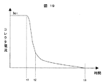
しかしながら、上述の図18のIGBTには、以下に示すような問題がある。図19に図18のIGBTのターンオフ時の主電流波形を示す。大きさIc1に流れていたコレクタ電流が時刻t1のIGBTオフにより減少し始める。しかし時刻t2になると電流の減少は緩やかになり時刻t3まで裾を引くようにゆっくりと減少してゆく。この時刻t2からt3の期間の電流をテール電流と呼ぶ。 However, the IGBT shown in FIG. 18 has the following problems. FIG. 19 shows a main current waveform when the IGBT of FIG. 18 is turned off. The collector current flowing in the magnitude Ic1 starts to decrease due to the IGBT off at time t1. However, at time t2, the decrease in current becomes gradual and gradually decreases so as to have a tail until time t3. The current during the period from time t2 to t3 is referred to as tail current.
テール電流は主にIGBT内部の残留キャリアによるもので、キャリアの残留領域すなわち図18のn- 層111の領域のキャリアの寿命により電流の大きさが決まる。この電流の低減のためには、図18のIGBTのn- 層111のキャリア濃度を大きくし、ライフタイムを小さくする方法があるが、特許文献1の(0020)段落に記載されている様に、n- 層111のキャリア濃度を大きくすると、ターンオフ時の跳ね上がり電圧を抑制できずRBSOAが狭くなる問題がある。加えて、エミッタ側のpn接合での電界が大きくなり耐圧が低下する問題もある。 The tail current is mainly due to the residual carriers in the IGBT, and the magnitude of the current is determined by the carrier lifetime in the carrier residual region, that is, the region of the n − layer 111 in FIG. In order to reduce this current, there is a method of increasing the carrier concentration of the n − layer 111 of the IGBT of FIG. 18 and reducing the lifetime, as described in paragraph (0020) of Patent Document 1. If the carrier concentration of the n − layer 111 is increased, the jumping voltage at the turn-off time cannot be suppressed and the RBSOA becomes narrow. In addition, there is a problem that the electric field at the pn junction on the emitter side increases and the breakdown voltage decreases.
本発明の目的は、上記課題を解決し、低い損失で信頼性が高い半導体装置とそれを用いた電力変換装置を提供することにある。 An object of the present invention is to solve the above problems and provide a semiconductor device with low loss and high reliability and a power conversion device using the same.
上記課題を解決するために、以下の構造を有する半導体装置およびそれを使った電力変換装置にすれば良い。すなわち、本発明のIGBTは、コレクタ側に基板よりも濃度が大きく深いn層をもち、かつコレクタ側に低スイッチング損失を実現する低注入のp層を備え、コレクタ側のp層のキャリア濃度の最大値が、そのp層に隣接するn層のキャリア濃度の最大値の10から100倍である。 In order to solve the above problems, a semiconductor device having the following structure and a power conversion device using the semiconductor device may be used. That is, the IGBT of the present invention has a p-layer of low injection that realizes a low switching loss on the collector side, and has an n-layer having a higher concentration and deeper than the substrate on the collector side. The maximum value is 10 to 100 times the maximum value of the carrier concentration of the n layer adjacent to the p layer.
本発明の半導体装置は、一対の主表面を有する半導体基体と、該基体内に位置する第1導電形の第1の半導体領域と、前記第1の半導体領域に隣接し第1の半導体領域のキャリア濃度より低いキャリア濃度を有する第2導電形の第2の半導体領域と、前記第2の半導体領域に隣接し第2の半導体領域のキャリア濃度より低いキャリア濃度を有する第2導電形の第3の半導体領域と、前記第3の半導体領域上に隣接し第3の半導体領域のキャリア濃度より低いキャリア濃度を有する第2導電形の第4の半導体領域と、前記第4の半導体領域内に伸びる複数個の第1導電形の第5の半導体領域と、該第5の半導体領域内に位置する第2の導電形の第6の半導体領域と、前記第4、第5及び第6の半導体領域の表面上に形成されたゲート絶縁膜と、さらに該絶縁膜上に形成されたゲート電極と、前記第5の半導体領域と第6の半導体領域に低抵抗接触したエミッタ電極と、前記第1の半導体領域に低抵抗接触したコレクタ電極とを有し、前記第1の半導体領域のキャリア濃度の最大値が、前記第2の半導体領域のキャリア濃度の最大値の10から100倍とすればよい。 A semiconductor device according to the present invention includes a semiconductor substrate having a pair of main surfaces, a first semiconductor region of a first conductivity type located in the substrate, and a first semiconductor region adjacent to the first semiconductor region. A second semiconductor region of a second conductivity type having a carrier concentration lower than the carrier concentration, and a third of a second conductivity type having a carrier concentration lower than the carrier concentration of the second semiconductor region adjacent to the second semiconductor region. , A fourth semiconductor region of a second conductivity type adjacent to the third semiconductor region and having a carrier concentration lower than that of the third semiconductor region, and extending into the fourth semiconductor region A plurality of first conductivity type fifth semiconductor regions; a second conductivity type sixth semiconductor region located in the fifth semiconductor region; and the fourth, fifth and sixth semiconductor regions. A gate insulating film formed on the surface of Furthermore, a gate electrode formed on the insulating film, an emitter electrode in low resistance contact with the fifth semiconductor region and the sixth semiconductor region, and a collector electrode in low resistance contact with the first semiconductor region And the maximum value of the carrier concentration of the first semiconductor region may be 10 to 100 times the maximum value of the carrier concentration of the second semiconductor region.
また、本発明の半導体装置はトレンチゲートを有する半導体装置であって、一対の主表面を有する半導体基体と、該基体内に位置する第1導電形の第1の半導体領域と、前記第1の半導体領域に隣接し第1の半導体領域のキャリア濃度より低いキャリア濃度を有する第2導電形の第2の半導体領域と、前記第2の半導体領域に隣接し第2の半導体領域のキャリア濃度より低いキャリア濃度を有する第2導電形の第3の半導体領域と、前記第3の半導体領域上に隣接し第3の半導体領域のキャリア濃度より低いキャリア濃度を有する第2導電形の第4の半導体領域と、前記第4の半導体領域内に延在し、少なくとも2種類の異なる隣り合う間隔を有する複数個のMOS形トレンチゲートと、該MOS形トレンチゲート間にあって前記第4の半導体領域のキャリア濃度より高いキャリア濃度を有する第1導電形の第5の半導体領域と、隣り合う間隔が狭いMOS形トレンチゲート間にあって前記第5の半導体領域内に位置するとともに前記MOS形トレンチゲートに接し第5の半導体領域のキャリア濃度より高いキャリア濃度を有する第2導電形の第6の半導体領域と、前記第5の半導体領域と第6の半導体領域に低抵抗接触したエミッタ電極と、前記第1の半導体領域に低抵抗接触したコレクタ電極とを有し、前記第1の半導体領域のキャリア濃度の最大値が、前記第2の半導体領域のキャリア濃度の最大値の10から100倍とすれば良い。 The semiconductor device of the present invention is a semiconductor device having a trench gate, a semiconductor substrate having a pair of main surfaces, a first semiconductor region of a first conductivity type located in the substrate, and the first A second semiconductor region of a second conductivity type adjacent to the semiconductor region and having a carrier concentration lower than that of the first semiconductor region; and lower than a carrier concentration of the second semiconductor region adjacent to the second semiconductor region A third semiconductor region of the second conductivity type having a carrier concentration, and a fourth semiconductor region of the second conductivity type having a carrier concentration lower than the carrier concentration of the third semiconductor region adjacent to the third semiconductor region; A plurality of MOS type trench gates extending in the fourth semiconductor region and having at least two different adjacent intervals, and the fourth semiconductor between the MOS type trench gates. A fifth semiconductor region of the first conductivity type having a carrier concentration higher than the carrier concentration of the region, and a MOS-type trench gate that is located between the adjacent MOS-type trench gates having a narrow interval and is located in the fifth semiconductor region; A sixth semiconductor region of a second conductivity type having a carrier concentration higher than a carrier concentration of the fifth semiconductor region, an emitter electrode in low-resistance contact with the fifth semiconductor region and the sixth semiconductor region, and A collector electrode in low resistance contact with one semiconductor region, and the maximum value of the carrier concentration of the first semiconductor region is 10 to 100 times the maximum value of the carrier concentration of the second semiconductor region. good.
さらに、前記第2の半導体領域のキャリア濃度の総和が1×1012cm-2から1×1013cm-2であることが望ましい。また、前記第1の半導体領域の厚さが3μm以下であればさらに望ましく、さらには前記第1の半導体領域に接するコレクタ電極がその接触面領域で少なくともアルミニウムを含有すればより好ましい。 Furthermore, it is desirable that the total carrier concentration of the second semiconductor region is 1 × 10 12 cm −2 to 1 × 10 13 cm −2 . Further, it is more desirable if the thickness of the first semiconductor region is 3 μm or less, and it is more preferable if the collector electrode in contact with the first semiconductor region contains at least aluminum in the contact surface region.
また、電力変換装置のスイッチング素子として上記半導体装置を用いる際は、併用する還流ダイオードが次の構造をもつと良い。すなわちダイオードの構造は、一対の主表面を有する半導体基体と、前記半導体基体の一方の主表面に隣接し該基体内に位置する第1導電形の第1の半導体領域と、前記第1の半導体領域に隣接し第1の半導体領域のキャリア濃度より低いキャリア濃度を有する第1導電形の第2の半導体領域と、前記第2の半導体領域上に隣接し第2の半導体領域のキャリア濃度より低いキャリア濃度を有する第1導電形の第3の半導体領域と、前記第1の半導体領域に隣接する第2導電形の第4の半導体領域と、前記第4の半導体領域に接触する第1の電極と、前記第1の半導体領域に接触する第2の電極とを有すればよい。さらに該ダイオードの高耐圧化や宇宙線耐量向上には、前記第2の半導体領域の厚さが前記第1の半導体領域の厚さより厚く前記第3の半導体領域の厚さより薄いことが望ましく、損失低減には前記第1の半導体領域のシートキャリア濃度が1×1012cm-2以下、ピーク濃度が1×1016cm-3以下であると良い。 Moreover, when using the said semiconductor device as a switching element of a power converter device, it is good for the free-wheeling diode used together to have the following structure. That is, the structure of the diode includes a semiconductor substrate having a pair of main surfaces, a first semiconductor region of a first conductivity type adjacent to one main surface of the semiconductor substrate and positioned in the substrate, and the first semiconductor A second semiconductor region of a first conductivity type adjacent to the region and having a carrier concentration lower than that of the first semiconductor region; and lower than a carrier concentration of the second semiconductor region adjacent to the second semiconductor region A third semiconductor region of a first conductivity type having a carrier concentration, a fourth semiconductor region of a second conductivity type adjacent to the first semiconductor region, and a first electrode in contact with the fourth semiconductor region And a second electrode in contact with the first semiconductor region. Further, in order to increase the breakdown voltage of the diode and improve the cosmic ray withstand capability, it is desirable that the thickness of the second semiconductor region is larger than the thickness of the first semiconductor region and thinner than the thickness of the third semiconductor region. For the reduction, the sheet carrier concentration of the first semiconductor region is preferably 1 × 10 12 cm −2 or less and the peak concentration is 1 × 10 16 cm −3 or less.
本発明によれば逆バイアス安全動作領域(RBSOA)を低下させることなくIGBTのターンオフ損失を低減できるので、電力変換装置の効率を向上できる。 According to the present invention, the IGBT turn-off loss can be reduced without lowering the reverse bias safe operation area (RBSOA), so that the efficiency of the power converter can be improved.
以下、本発明の詳細を図面を用いながら説明する。 The details of the present invention will be described below with reference to the drawings.
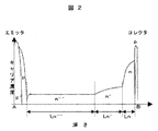
図1は、本実施例のIGBTの断面構造図を示す。図1において、図18と同じ構成要素には同一の符号を付してある。図2は、図1のA−B間における濃度プロファイルを示し、図3は、図1のIGBTのターンオフ波形の例を示す。図1において、符号112は低キャリア濃度のn層、100は低キャリア濃度のp層である。
FIG. 1 shows a cross-sectional structure diagram of the IGBT of this embodiment. In FIG. 1, the same components as those in FIG. 18 are denoted by the same reference numerals. 2 shows a concentration profile between A and B in FIG. 1, and FIG. 3 shows an example of the turn-off waveform of the IGBT in FIG. In FIG. 1,
図1に示すIGBTの特徴は、p層100、n層112のキャリア濃度が前記従来技術のIGBTより低く、かつn-層111を備えた点にある。p層100のキャリア濃度が低いとp層100からのホールの注入が抑えられ、n層112、n- 層111のキャリア濃度が低くなる。n-層111のキャリア濃度が低くなるとターンオフ時のn-層111内の残留キャリアが少なくなり、テール電流が減少する。これによりターンオフ時の電流波形が図3の実線で示す波形となり、テール期間Taが、破線で示した従来技術のIGBTのテール期間Tbより短くなって損失を低減できる。また、本実施例ではライフタイムの長いn- 層111があるため、急激なテール電流の減少を抑制でき、跳ね上がり電圧の発生しないターンオフ特性を実現できる。
The IGBT shown in FIG. 1 is characterized in that the carrier concentration of the
本実施例のIGBTで、高破壊耐量、高耐圧、低損失を同時に実現するためには、p層100のキャリア濃度をn層112のキャリア濃度の10倍〜100倍の範囲にすることが好ましく、特にn層112のキャリア濃度の総和(シートキャリア濃度)を1×1012cm-2〜1×1013cm-2、p層100の厚さを3μm以下とするとさらに効果的である。この理由を以下に述べる。
In the IGBT of this embodiment, in order to simultaneously realize a high breakdown strength, a high breakdown voltage, and a low loss, it is preferable that the carrier concentration of the
p層100のキャリア濃度がn層112のキャリア濃度の10倍未満の場合には、p層100からのキャリアの注入が少なくなる。この場合にはn- 層111内のキャリア濃度も少なくなるために、ターンオフ時にp層120とn--層110の接合からn--層110内に伸びる空乏層がn- 層111に到達すると急激に電流が減少して跳ね上がり電圧が発生する。また、p層100のキャリア濃度がn層112のキャリア濃度の100倍以上になると、p層100からのキャリアの注入が大きくなり過ぎ、テール電流が増えて損失が増大する。従って、p層100とn層112のキャリア濃度の関係は10倍〜100倍の範囲に設定することが好ましい。
When the carrier concentration of the
次に、n層112のキャリア濃度が1012cm-2未満になると、過電圧がIGBTに印加され空乏層がn層112に到達した時に、空乏層がp層100に伸びることを抑制できず、空乏層がp層100に到達してパンチスルー現象が発生する。パンチスルー現象が発生すると電流が流れ始め、IGBTがスイッチとして機能しなくなる。一方、n層112のキャリア濃度が1×1013cm-2より高くなると、p層100のキャリア濃度を1×1014cm-2より高くしなければならず、様々な製造上の問題が発生する。例えば、キャリア濃度1×1014cm-2以上のp層100をボロンなどの不純物打ち込み法で作ると、イオンの打ち込み量が多くなるためにシリコン半導体基板の結晶欠陥が増大し、漏れ電流が多くなる。このように、n層112のキャリア濃度には好ましい範囲がある事が発明者らの実験で明らかとなった。
Next, when the carrier concentration of the
また、p層100の厚みを3μm以下にすると、キャリア濃度を低減しなくてもp層
100からのキャリアの注入を低減でき、上述した不純物の打ち込み量を減らして、漏れ電流を低減できる。ここで、p層100の厚みは3μm〜0.3μm が好ましく、3μm〜1μmがさらに好ましい。p層100の厚みが0.3μm 未満ではコレクタ電極500との電気的な接触が不良になる場合がある。
Further, when the thickness of the
さらには、コレクタ電極500に接するp層100では、表面のキャリア濃度が低いため、コレクタ電極500に使う金属の種類によっては接触抵抗が大きくなる。そこで、コレクタ電極にp形不純物、例えばアルミニウムあるいはアルミニウム、を含む合金を適用すれば、p層100との接触抵抗を低減できることが分かった。本発明者らの実験で、アルミニウムをコレクタ電極500の一部として使えば、低濃度のp層100との電気的接触も問題なく、半導体装置の損失低減や電力変換装置の短絡耐量を確保出来ることが分かった。
Furthermore, since the p-
加えて図1の構造のIGBTの耐圧向上を検討した結果、次のことも分かった。n--層110の厚さをLn--、n-層111の厚さをLn-、n層112の厚さをLnとしたとき、Ln-->Ln->Lnとすることで、n--層110とp層120の境界の電界強度が低減され、耐圧が向上する。また、特に5kV〜6kV程度以上の耐圧をもつ半導体装置では、宇宙線による破壊頻度が高くなることが知られているが、本実施例のIGBTでは宇宙線耐量も向上していることが分った。なお、各層の厚さをLn-->Ln- >Lnとすることによって、p層100、n層112のキャリア濃度が高い場合にも耐圧が向上することを確認した。
In addition, as a result of examining the breakdown voltage improvement of the IGBT having the structure of FIG. When the thickness of the n − layer 110 is Ln − , the thickness of the n − layer 111 is Ln − , and the thickness of the
なお、耐圧が低くても良く、宇宙線耐量の考慮は不要なIGBTでは、n-層111の厚さLn-は厚くし、コレクタエミッタ間のシリコン基板全体の厚さを薄くして、導通損失を低減できる。 In IGBTs that may have a low breakdown voltage and do not require consideration of cosmic ray withstand capability, the thickness Ln − of the n − layer 111 is increased, and the entire thickness of the silicon substrate between the collector and emitter is reduced to reduce the conduction loss. Can be reduced.
図4は、本実施例のIGBT断面構造図を示す。図4では、図1と同じ構成要素には同一の符号を付してある。図4の構造は、n--層110より高い濃度のn層150を備えることが実施例1の図1と異なり、その他は同じである。p層100から注入されるプラスのキャリア、すなわちホールは、n層112、n- 層111、n--層110、p層120、p+ 層121を通ってエミッタ電極600に流れる。n層150が形成されると、n層150はn--層110よりもホールにとってのポテンシャル障壁が高いため、ホールがp層120に流れにくくなり、ホールがn--層110に蓄積される。n--層110にホールが蓄積されると導通状態の抵抗が小さくなり、導通損失を低減できる。
FIG. 4 shows an IGBT cross-sectional structure diagram of the present embodiment. In FIG. 4, the same components as those in FIG. The structure of FIG. 4 is the same as FIG. 1 of the first embodiment except that the
低注入のp層100ではホールの注入が減少するため、n--層110に蓄積されるキャリアが減り、導通損失が増える場合があるが、本実施例によれば、p層100の注入を低減しても、n層150によりn--層110にホールが蓄積されるために導通損失が増えない。
Since the injection of low implantation of p-
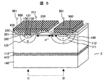
図5は、本実施例のIGBTの断面構造図を示す。図5では、図1,図4と同じ構成要素には同一の符号を付してある。図5において、符号10は絶縁膜、140は半導体基板である。図5構造の特徴は、コレクタ電極500とエミッタ電極600が同一表面に形成されているいわゆるラテラル型のIGBTである。n--層110は半導体基板140と絶縁膜410で電気的に分離されている。このような構造は、同一表面上にすべての電極が配置されているので、同一チップ内に保護回路や駆動回路などの集積化が可能となり、高電圧LSIなどに好適である。本実施例でも、実施例1や実施例2と同様、低濃度のp層100、n層112およびn- 層111により、ターンオフ損失を低減する。さらに半導体基板140をエミッタ電極と同電位とすることで、RESURF効果と呼ばれる耐圧向上効果も与えることができる。また、このRESURF効果では、p層120直下での電界集中を引き起こすことがあるが、コレクタ電極とエミッタ電極の電位の間の任意の電位とすることで、さらに耐圧を向上できる。
FIG. 5 shows a cross-sectional structure diagram of the IGBT of this embodiment. 5, the same components as those in FIGS. 1 and 4 are denoted by the same reference numerals. In FIG. 5, reference numeral 10 denotes an insulating film and 140 denotes a semiconductor substrate. 5 is a so-called lateral IGBT in which the
図6は、本実施例のIGBT断面構造図を示す。図6では、図1、図4、図5と同じ構成要素には同一の符号を付してある。本実施例では、実施例3の構造に加え、図6に示すn--層110より濃度の高いn層150を配置した。図6に示す本実施例では、実施例2と同様、n層150によりn--層110にキャリアが蓄積されるため、導通損失を低減できる。さらに半導体基板140をエミッタ電極と同電位とすることで、RESURF効果と呼ばれる耐圧向上効果も与えることができる。また、このRESURF効果では、p層120直下での電界集中を引き起こすことがあるが、コレクタ電極とエミッタ電極の電位の間の任意の電位とすることで、さらに耐圧を向上できる。
FIG. 6 shows an IGBT cross-sectional structure diagram of the present embodiment. In FIG. 6, the same components as those in FIGS. 1, 4 and 5 are denoted by the same reference numerals. In this example, in addition to the structure of Example 3, an
図7は本実施例のIGBTの断面構造図を示す。図7では、図1と同じ構成要素には同一の符号を付してある。図7で、符号125はp層、401、402は絶縁膜である。本実施例では、トレンチゲート型IGBTに低濃度のp層100とn層112及び、n-層111を設けた。図7で、エミッタ電極600は隣り合うトレンチ形MOSゲート(ゲート電極200、ゲート絶縁膜300)間の距離が短い領域のp+層121とn+層130とに電気的に接触している。この断面では、隣り合うトレンチ形ゲート間が広い部分のp層125は、絶縁膜401、402でエミッタ電極600と絶縁分離され、p層125はフローティング電位となっている。この結果、p層100から注入したホールの一部が、一旦p層125に流れ込み、トレンチ形MOSゲートの底に沿うように流れ、p層120、p+ 層121、エミッタ電極600へ流入する。その結果、このホールがバイポーラトランジスタのベース電流のような働きをし、トレンチ形MOSゲートの底部に形成された蓄積層から電子がn--層110へ注入し、n--層110の伝導度変調が促進される。これにより本実施例のIGBTは損失が低くなる。
FIG. 7 shows a cross-sectional structure diagram of the IGBT of this embodiment. In FIG. 7, the same components as those in FIG. In FIG. 7,
本実施例は実施例2と同様に、低濃度のp層100でキャリアの注入が減少し定常損失が増大する場合でも、上述の伝導度変調の促進により導通損失の増大を回避できる。
In the present embodiment, similarly to the second embodiment, even when the carrier injection is reduced and the steady loss is increased in the low-
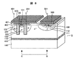
図8は、本実施例のIGBTの断面構造図を示す。図8で、図5や図7と同じ構成要素には同一の符号を付してある。本実施例のIGBTは、実施例5のトレンチゲート型の構造を高圧LSI用に適用しやすいコレクタ電極500とエミッタ電極600が、同一表面上に形成された、いわゆるラテラル型の半導体装置6である。コレクタ側に面した領域にフローティングのp層125が形成されており、実施例3で述べた伝導度変調の向上効果が実現できるとともに、高電圧LSIの高集積化が可能である。また、本実施例ではp層125を設けることにより、ゲート絶縁膜300に加わる電界、特にコレクタ側の電界を緩和でき、ゲート絶縁膜300の信頼性を高くできる。
FIG. 8 shows a cross-sectional structure diagram of the IGBT of the present embodiment. In FIG. 8, the same components as those in FIGS. 5 and 7 are denoted by the same reference numerals. The IGBT of this embodiment is a so-called lateral type semiconductor device 6 in which a
図9に本実施例のIGBTの断面構造図を示す。図9で、実施例5の図7と同じ構成要素には同一の符号を付してある。本実施例のIGBTは、図7に示す実施例5のIGBTにn層151を加えたことが異なり、その他は同様である。隣り合うトレンチ形MOSゲート間の距離が短い領域のp層120とn--層110の間に設けたn層151は、実施例2のn層150と同様の効果を持ち、n--層110にホールを蓄積し、さらなる導通損失を低減する。
FIG. 9 shows a cross-sectional structure diagram of the IGBT of this embodiment. In FIG. 9, the same components as those in FIG. 7 of the fifth embodiment are denoted by the same reference numerals. The IGBT of the present embodiment is the same as the IGBT of the fifth embodiment shown in FIG. 7 except that an
図10に本実施例のIGBTの断面構造図を示す。図10で、実施例6の図8と同じ構成要素には同一の符号を付してある。図10に示す本実施例では、実施例6の図8のIGBTにn層151を加えたことが異なり、その他は同様である。隣り合うトレンチ形MOSゲート間の距離が短い領域のp層120とn--層110の間に設けたn層151は、実施例2のn層150と同様の効果を持ち、n--層110にホールを蓄積し、さらなる導通損失を低減する。
FIG. 10 shows a cross-sectional structure diagram of the IGBT of this embodiment. In FIG. 10, the same components as those in FIG. 8 of the sixth embodiment are denoted by the same reference numerals. In this embodiment shown in FIG. 10, the difference is that the
図11は、本実施例の電力変換装置のインバータ部の回路構成を示す。図12と図13は本実施例の電力変換装置に用いるダイオードの断面構造図である。図11に示す電力変換装置では、電力半導体スイッチング素子であるIGBT701〜706に実施例1から実施例8に記載の構造のIGBTを使い、ダイオード711〜716に図12、図13に示した構造のダイオードを適用した。IGBTチップとダイオードチップは、いわゆるIGBTモジュールとして金属ベース上に配置したセラミックス回路基板に搭載し、樹脂ケースに収容あるいは、樹脂モールドされている。
FIG. 11 shows the circuit configuration of the inverter unit of the power conversion device of this embodiment. 12 and 13 are cross-sectional structural views of a diode used in the power converter of this embodiment. In the power conversion device shown in FIG. 11, the IGBTs having the structures described in the first to eighth embodiments are used for the
図11で、符号801〜806はゲート回路、900はP端子、901はN端子でこれらの端子に直流電源が接続される。また、図11で符号910はU端子、911はV端子、912はW端子である。本実施例では図11に示すように、2つのIGBTが直列に接続されたアームを3つ備え、各アームの上アームと下アームのIGBTの接続点がそれぞれU端子910、V端子911、W端子912に接続し、これらの3つの端子から3相交流電力が負荷であるモータ950に出力される。
In FIG. 11,
図12は本実施例の電力変換装置のIGBTに逆並列に接続した還流ダイオードの断面図であって、符号510はカソード電極、102はn層、111はn層102より濃度の低いn-層、110はn-層111より濃度の低いn--層、160はp層、610はp層160と低抵抗接触するアノード電極、511はカソード端子、611はアノード端子である。
FIG. 12 is a cross-sectional view of a free-wheeling diode connected in reverse parallel to the IGBT of the power conversion device of this embodiment.
また、図13は低注入アノード構造を持つダイオードの断面構造であって、図12と同一の構成要素には同じ符号を付してある。図13で、符号162はp層、161はアノード電極610とショットキー接触した低濃度p-層である。
FIG. 13 is a cross-sectional structure of a diode having a low injection anode structure, and the same components as those in FIG. In FIG. 13,
図12、図13のダイオードは通電状態から逆方向電圧の印加状態に移行するいわゆるリバースリカバリ時にアノード側のpn接合からn--層110に伸びる空乏層がn層102に到達することを、n- 層111で防止する構造となっている。これにより、リバースリカバリー時に発生する電流振動やそれに伴う過電圧の発生を防止している。
12 and 13 indicate that the depletion layer extending from the pn junction on the anode side to the n − layer 110 reaches the
図11の電力変換装置では図12もしくは図13のダイオードを実施例1から実施例8のIGBTと組み合わせて使うことにより、インバータ部の低損失化と、高信頼化を実現している。図11で、本発明のスイッチング素子だけを適用する場合には、例えば、IGBTだけ本発明の構造を適用してもよいが、ダイオードがリバースリカバリー時に電流振動や電圧の跳ね上がりなどを引き起こすために、IGBTのターンオンスピードを緩やかにしなければならず、本発明のIGBTの性能を完全に発揮できない。本発明のIGBTの性能を最大限に発揮するには、図12、図13に示すダイオードと組み合わせると良い。なお、図11のインバータ装置の構成は一例であって、例えば、スイッチング素子とダイオードが逆並列された上下のアームの直列組み合わせが、交流出力の相数と同数結合されたインバータ装置であれば同様である。 In the power conversion device of FIG. 11, by using the diode of FIG. 12 or FIG. 13 in combination with the IGBTs of the first to eighth embodiments, low loss and high reliability of the inverter unit are realized. In FIG. 11, when only the switching element of the present invention is applied, for example, the structure of the present invention may be applied only to the IGBT. However, in order for the diode to cause current oscillation or voltage jump during reverse recovery, The turn-on speed of the IGBT must be made slow, and the performance of the IGBT of the present invention cannot be fully exhibited. In order to maximize the performance of the IGBT of the present invention, the diodes shown in FIGS. 12 and 13 may be combined. The configuration of the inverter device in FIG. 11 is an example. For example, the same is true if the series combination of the upper and lower arms in which switching elements and diodes are anti-parallel is coupled in the same number as the number of AC output phases. It is.
図11に示した本実施例の電力変換装置を構成するスイッチング素子とダイオードは、図14に示す同じ構成の半導体基板、例えばシリコン基板から作製できる。図14で、符号102はn層、111はn層102より濃度の低いn-層、110はn-層111より濃度の低いn--層である。図15は、図14のA−B間の濃度分布を示す。
The switching element and the diode constituting the power conversion device of this embodiment shown in FIG. 11 can be manufactured from a semiconductor substrate having the same configuration shown in FIG. 14, for example, a silicon substrate. In Figure 14,
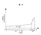
また、図14に示す半導体基板は、図15に示すキャリア濃度分布に加え、図16および図17に示すようなキャリア濃度分布を持つ基板であっても良い。図16に示す半導体基板の特徴は、n--層110とn- 層111の明確な境界はないが、AからBへキャリア濃度が連続して緩やかに増加している。
Further, the semiconductor substrate shown in FIG. 14 may be a substrate having a carrier concentration distribution as shown in FIGS. 16 and 17 in addition to the carrier concentration distribution shown in FIG. Wherein the semiconductor substrate shown in FIG. 16, n - layer 110 and the n - but
図17に示す半導体基板では、AからBへキャリア濃度が複数の層、この場合は濃度が異なる2つのn -層を経て増加していく点に特徴がある。図16、図17に示すこれら基板の製造は、イオン打ち込みやエピタキシャル成長、熱拡散などの適用により可能で、形成は図14のn--層110側からでも、n層102側からでもよい。またn102層は、n--層110およびn-層111に比べて層の厚さが薄いので、製造工程の任意の段階で形成してもよい。
The semiconductor substrate shown in FIG. 17 is characterized in that the carrier concentration increases from A to B through a plurality of layers, in this case through two n − layers having different concentrations. These substrates shown in FIGS. 16 and 17 can be manufactured by ion implantation, epitaxial growth, thermal diffusion, or the like, and can be formed from the n − layer 110 side or the
IGBTとダイオードを組み合わせて用いる場合、例えばパワーモジュールとして用いる場合には、ダイオードの耐圧や宇宙線耐量などの特性が低いと全体の信頼性が低下する。しかし、図15のn--層厚さLn--、n-層厚さLn-、n層厚さLnがLn-->Ln->Lnの大小関係を満たすとき、ダイオードもIGBTと同様に高耐圧、高宇宙線耐量の効果が得られることを、本発明者は確認した。また、ダイオードのさらなる低損失化には、n-層濃度のシートキャリア濃度を1×1012cm-2以下とするか、ピーク濃度が1×1016cm-3以下とするか、あるいは両者を満たすことが望ましい。これによりカソードからのキャリア注入が抑えられ、ダイオードのオフ時の損失が低減される。 When the IGBT and the diode are used in combination, for example, when used as a power module, if the characteristics such as the withstand voltage and the cosmic ray withstand capability of the diode are low, the overall reliability is lowered. However, n in FIG. 15 - layer thickness Ln -, n - layer thickness Ln -, n layer thickness Ln is Ln -> Ln - when> satisfy the magnitude relationship of Ln, the diode also like the IGBT The present inventor has confirmed that the effect of high withstand voltage and high cosmic ray tolerance can be obtained. In order to further reduce the loss of the diode, the sheet carrier concentration of the n − layer concentration is set to 1 × 10 12 cm −2 or less, or the peak concentration is set to 1 × 10 16 cm −3 or less. It is desirable to satisfy. Thereby, carrier injection from the cathode is suppressed, and the loss when the diode is off is reduced.
以上、本実施例では直流を交流に変換するインバータについて説明したが、もちろんこれに限定されるものではなく、交流を直流に変換するコンバータについても同様である。 As described above, in the present embodiment, the inverter that converts direct current into alternating current has been described, but of course, the present invention is not limited to this, and the same applies to a converter that converts alternating current into direct current.
1、2、3、4、5、6、7、8、20、30、40…半導体装置、50、140…半導体基板、100、120、125、160、162…p層、101、121…p+層、102、112、150、151…n層、110…n--層、111…n-層、113、130…n+層、161…p-層、200…ゲート電極、201…ゲート端子、300…ゲート絶縁膜、301…厚いゲート絶縁膜、400、401、402、410…絶縁膜、500…コレクタ電極、501…コレクタ端子、510…カソード電極、511…カソード端子、600…エミッタ電極、601…エミッタ端子、610…アノード電極、611…アノード端子、701、702、703、704、705、706…IGBT、711、712、713、714、715、716…ダイオード、801、802、803、804、805、806…ゲート回路、900…P端子、901…N端子、910…U端子、911…V端子、912…W端子、950…モータ。
1, 2, 3, 4, 5, 6, 7, 8, 20, 30, 40 ... semiconductor device, 50, 140 ... semiconductor substrate, 100, 120, 125, 160, 162 ... p layer, 101, 121 ... p + layer, 102,112,150,151 ... n layer, 110 ... n - layer 111 ... n - layer, 113,130 ... n + layer, 161 ... p - layer, 200 ... gate electrode, 201 ... gate terminal , 300 ... gate insulating film, 301 ... thick gate insulating film, 400, 401, 402, 410 ... insulating film, 500 ... collector electrode, 501 ... collector terminal, 510 ... cathode electrode, 511 ... cathode terminal, 600 ... emitter electrode, 601...
Claims (4)
交流の相数と同数の交流端子と、
電力半導体スイッチング素子と逆極性のダイオードの並列回路を2個直列接続し、該直列接続した一端と他端とを前記一対の直流端子に接続し、
前記電力半導体スイッチング素子と逆極性のダイオードの並列回路の直列接続点を前記交流端子に接続する電力変換装置において、
前記電力半導体スイッチング素子が、
一対の主表面を有する、
半導体基体の主表面に隣接し前記半導体基体内に位置する第1導電形の第1の半導体領域と、
前記第1の半導体領域に隣接し第1の半導体領域のキャリア濃度より低いキャリア濃度を有する第2導電形の第2の半導体領域と、
前記第2の半導体領域と隣接し第2の半導体領域のキャリア濃度より低いキャリア濃度を有する第2導電形の第3の半導体領域と、
前記第3の半導体領域と隣接し第3の半導体領域のキャリア濃度より低いキャリア濃度を有する第2導電形の第4の半導体領域と、
前記半導体基体の主表面より前記第4の半導体領域内に伸びる第1導電形の第5の半導体領域と、
前記半導体基体の主表面より該第5の半導体領域内に伸びる第2導電形の第6の半導体領域と、
前記第4と第6の半導体領域の間の第5の半導体領域の主表面の露出部分に形成された絶縁膜と、
該絶縁膜上に形成された第1の電極と、
前記第5の半導体領域と第6の半導体領域に接触する第2の電極と、
前記第1の半導体領域に接触する第3の電極とを有し、
前記第1の半導体領域のキャリア濃度の最大値が、前記第2の半導体領域のキャリア濃度の最大値の10倍〜100倍であり、
前記第2の半導体領域の厚さが前記第3の半導体領域より薄く、前記第3の半導体領域の厚さが前記第4の半導体領域より薄く、前記第2の半導体領域のキャリア濃度の総和が1×10 12 cm -2 から1×10 13 cm -2 である半導体装置であり、
前記ダイオードが、
第2導電形の第8の半導体領域と、
前記第8の半導体層に隣接し前記第8の半導体領域のキャリア濃度より低いキャリア濃度を有する第2導電形の第9の半導体領域と、
前記第9の半導体層に隣接し前記第9の半導体領域のキャリア濃度より低いキャリア濃度を有する第2導電形の第10の半導体領域と、
前記第10の半導体層に隣接する第1導電形の第11の半導体領域と、
前記第8の半導体領域に接触する第4の電極と、
前記第11の半導体領域に接触する第5の電極と、
を備え、
前記第8の半導体領域の厚さが前記第9の半導体領域より薄く、前記第9の半導体領域の厚さが前記第10の半導体領域より薄く、前記第9の半導体領域のピーク濃度が1×10 16 cm -3 以下であることを特徴とする電力変換装置。 A pair of DC terminals;
AC terminals with the same number of AC phases,
Two parallel circuits of power semiconductor switching elements and diodes of opposite polarity are connected in series, and one end and the other end connected in series are connected to the pair of DC terminals,
In the power converter for connecting a series connection point of a parallel circuit of a diode of reverse polarity with the power semiconductor switching element to the AC terminal,
The power semiconductor switching element is
Having a pair of main surfaces,
A first semiconductor region of a first conductivity type located adjacent to the main surface of the semiconductor substrate and located within the semiconductor substrate;
A second semiconductor region of a second conductivity type adjacent to the first semiconductor region and having a carrier concentration lower than that of the first semiconductor region;
A third semiconductor region of a second conductivity type adjacent to the second semiconductor region and having a carrier concentration lower than that of the second semiconductor region;
A fourth semiconductor region of a second conductivity type adjacent to the third semiconductor region and having a carrier concentration lower than that of the third semiconductor region;
A fifth semiconductor region of a first conductivity type extending from the main surface of the semiconductor substrate into the fourth semiconductor region;
A sixth semiconductor region of a second conductivity type extending from the main surface of the semiconductor substrate into the fifth semiconductor region;
An insulating film formed on an exposed portion of the main surface of the fifth semiconductor region between the fourth and sixth semiconductor regions;
A first electrode formed on the insulating film;
A second electrode in contact with the fifth semiconductor region and the sixth semiconductor region;
A third electrode in contact with the first semiconductor region;
The maximum value of the carrier concentration of the first semiconductor region is 10 to 100 times the maximum value of the carrier concentration of the second semiconductor region;
The sum of the second thinner than the thickness the third semiconductor region of the semiconductor region, the third thickness of the semiconductor region is rather thin than the fourth semiconductor region, the carrier concentration of said second semiconductor region Is a semiconductor device having 1 × 10 12 cm −2 to 1 × 10 13 cm −2 ,
The diode is
An eighth semiconductor region of the second conductivity type;
A ninth semiconductor region of a second conductivity type adjacent to the eighth semiconductor layer and having a carrier concentration lower than that of the eighth semiconductor region;
A tenth semiconductor region of a second conductivity type adjacent to the ninth semiconductor layer and having a carrier concentration lower than that of the ninth semiconductor region;
An eleventh semiconductor region of a first conductivity type adjacent to the tenth semiconductor layer;
A fourth electrode in contact with the eighth semiconductor region;
A fifth electrode in contact with the eleventh semiconductor region;
With
The eighth thinner than the thickness ninth semiconductor region of the semiconductor region of the ninth thickness of the semiconductor region is rather thin than the tenth semiconductor regions, the peak concentration of the ninth semiconductor region 1 × 10 16 cm -3 or less
前記第5の半導体領域が前記半導体基体の他方の主表面から前記第4の半導体領域内に伸び、
前記第6の半導体領域が前記半導体基体の他方の主表面から前記第5の半導体領域内に伸びることを特徴とする電力変換装置。 The power conversion device according to claim 1, wherein the power semiconductor switching element has the first semiconductor region adjacent to one main surface of the semiconductor substrate,
The fifth semiconductor region extends from the other main surface of the semiconductor substrate into the fourth semiconductor region;
The power conversion device, wherein the sixth semiconductor region extends from the other main surface of the semiconductor substrate into the fifth semiconductor region.
前記第5の半導体領域が前記半導体基板の他方の主表面から前記第4の半導体領域内に伸び、
前記第6の半導体領域が前記半導体基板の他方の主表面から前記第5の半導体領域内に伸び、
前記第3の電極が前記第2の電極から離間し、前記第1の半導体領域に接触することを特徴とする電力変換装置。 The power conversion device according to claim 1, wherein the power semiconductor switching element has the first semiconductor region adjacent to the other main surface of the semiconductor substrate,
The fifth semiconductor region extends from the other main surface of the semiconductor substrate into the fourth semiconductor region;
The sixth semiconductor region extends from the other main surface of the semiconductor substrate into the fifth semiconductor region;
The power conversion device, wherein the third electrode is separated from the second electrode and is in contact with the first semiconductor region.
前記第5の半導体領域が前記半導体基体の他方の主表面から前記第4の半導体領域内に伸び、
前記第1の電極が、前記半導体基体の他方の主表面から前記第4の半導体領域内に伸びる少なくとも2種類の異なる間隔を有する複数のMOS形トレンチゲート電極であり、
前記第6の半導体領域が、前記半導体基体の他方の主表面から前記第5の半導体領域内に伸びることを特徴とする電力変換装置。 The power conversion device according to claim 1, wherein the power semiconductor switching element has the first semiconductor region adjacent to one main surface of the semiconductor substrate,
The fifth semiconductor region extends from the other main surface of the semiconductor substrate into the fourth semiconductor region;
The first electrode is a plurality of MOS trench gate electrodes having at least two different distances extending from the other main surface of the semiconductor substrate into the fourth semiconductor region;
The power converter according to claim 6, wherein the sixth semiconductor region extends from the other main surface of the semiconductor substrate into the fifth semiconductor region.
Priority Applications (3)
| Application Number | Priority Date | Filing Date | Title |
|---|---|---|---|
| JP2005116406A JP5135666B2 (en) | 2005-04-14 | 2005-04-14 | Power converter |
| EP10009398A EP2256813A3 (en) | 2005-04-14 | 2006-04-11 | Electric power conversion device |
| EP20060007623 EP1713128B1 (en) | 2005-04-14 | 2006-04-11 | IGBT and electric power conversion device using it |
Applications Claiming Priority (1)
| Application Number | Priority Date | Filing Date | Title |
|---|---|---|---|
| JP2005116406A JP5135666B2 (en) | 2005-04-14 | 2005-04-14 | Power converter |
Publications (3)
| Publication Number | Publication Date |
|---|---|
| JP2006295014A JP2006295014A (en) | 2006-10-26 |
| JP2006295014A5 JP2006295014A5 (en) | 2008-03-27 |
| JP5135666B2 true JP5135666B2 (en) | 2013-02-06 |
Family
ID=36691439
Family Applications (1)
| Application Number | Title | Priority Date | Filing Date |
|---|---|---|---|
| JP2005116406A Active JP5135666B2 (en) | 2005-04-14 | 2005-04-14 | Power converter |
Country Status (2)
| Country | Link |
|---|---|
| EP (2) | EP1713128B1 (en) |
| JP (1) | JP5135666B2 (en) |
Families Citing this family (9)
| Publication number | Priority date | Publication date | Assignee | Title |
|---|---|---|---|---|
| JP4957840B2 (en) * | 2010-02-05 | 2012-06-20 | 株式会社デンソー | Insulated gate semiconductor device |
| CN102254942A (en) * | 2011-07-27 | 2011-11-23 | 江苏物联网研究发展中心 | Novel Insulated Gate Bipolar Transistor (IGBT) with stepped gate structure and manufacturing method thereof |
| CN102412266B (en) * | 2011-10-13 | 2014-12-10 | 上海华虹宏力半导体制造有限公司 | Power device structure capable of improving safety operation region (SOA) capacity and manufacturing method |
| CN103165651A (en) * | 2011-12-12 | 2013-06-19 | 上海华虹Nec电子有限公司 | Insulated gate bipolar transistor (IGBT) structure for enhancing drive current capacity |
| JP5719407B2 (en) * | 2013-05-31 | 2015-05-20 | ローム株式会社 | Semiconductor device |
| CN104241346B (en) * | 2013-06-21 | 2017-03-15 | 上海北车永电电子科技有限公司 | Igbt and preparation method thereof |
| JP2016066701A (en) * | 2014-09-25 | 2016-04-28 | 株式会社日立製作所 | Semiconductor device and power converter using the same |
| DE102016111844A1 (en) | 2016-06-28 | 2017-12-28 | Infineon Technologies Ag | Power semiconductor device |
| JP6869791B2 (en) | 2017-04-21 | 2021-05-12 | 三菱電機株式会社 | Semiconductor switching elements and their manufacturing methods |
Family Cites Families (13)
| Publication number | Priority date | Publication date | Assignee | Title |
|---|---|---|---|---|
| FR2524715A1 (en) * | 1982-03-30 | 1983-10-07 | Thomson Csf | FAST DIODE |
| JPH0642542B2 (en) * | 1988-04-08 | 1994-06-01 | 株式会社東芝 | High-voltage semiconductor device manufacturing method |
| JPH08227999A (en) * | 1994-12-21 | 1996-09-03 | Mitsubishi Electric Corp | Integrated gate bipolar transistor and its manufacture and semiconductor integrated circuit and its manufacture |
| EP0837508A3 (en) * | 1996-10-18 | 1999-01-20 | Hitachi, Ltd. | Semiconductor device and electric power conversion apparatus therewith |
| JPH10189956A (en) | 1996-12-25 | 1998-07-21 | Hitachi Ltd | Semiconductor device |
| JP3287269B2 (en) * | 1997-06-02 | 2002-06-04 | 富士電機株式会社 | Diode and manufacturing method thereof |
| US6271061B1 (en) * | 1997-12-03 | 2001-08-07 | Stmicroelectronics S.R.L. | Fabrication of insulated gate bipolar devices |
| JP4164962B2 (en) * | 1999-10-08 | 2008-10-15 | 株式会社デンソー | Insulated gate bipolar transistor |
| JP4031209B2 (en) * | 2000-03-14 | 2008-01-09 | 株式会社東芝 | Semiconductor device |
| JP3764343B2 (en) * | 2001-02-28 | 2006-04-05 | 株式会社東芝 | Manufacturing method of semiconductor device |
| JP2003347549A (en) * | 2002-05-31 | 2003-12-05 | Hitachi Ltd | Semiconductor device and power conversion equipment using the same |
| JP3951868B2 (en) * | 2002-09-12 | 2007-08-01 | 富士電機デバイステクノロジー株式会社 | Semiconductor device and manufacturing method thereof |
| JP2006173297A (en) * | 2004-12-15 | 2006-06-29 | Denso Corp | Igbt |
-
2005
- 2005-04-14 JP JP2005116406A patent/JP5135666B2/en active Active
-
2006
- 2006-04-11 EP EP20060007623 patent/EP1713128B1/en not_active Revoked
- 2006-04-11 EP EP10009398A patent/EP2256813A3/en not_active Withdrawn
Also Published As
| Publication number | Publication date |
|---|---|
| EP1713128B1 (en) | 2011-07-06 |
| EP2256813A3 (en) | 2012-09-05 |
| EP1713128A1 (en) | 2006-10-18 |
| JP2006295014A (en) | 2006-10-26 |
| EP2256813A2 (en) | 2010-12-01 |
Similar Documents
| Publication | Publication Date | Title |
|---|---|---|
| JP6846119B2 (en) | Diode and power converter using it | |
| JP4843253B2 (en) | Power semiconductor device | |
| JP4644730B2 (en) | Semiconductor device and power conversion device using the same | |
| JP5135666B2 (en) | Power converter | |
| KR101309674B1 (en) | Insulated gate bipolar transistor and manufacturing method thereof | |
| US8928030B2 (en) | Semiconductor device, method for manufacturing the semiconductor device, and method for controlling the semiconductor device | |
| JP2005317751A (en) | Inversely conductive semiconductor device and its manufacturing method | |
| JP5963385B2 (en) | Semiconductor device | |
| JP2007258363A (en) | Semiconductor device | |
| JP5875680B2 (en) | Insulated gate bipolar transistor | |
| US20120273897A1 (en) | Semiconductor Device and Electric Power Conversion Device Using Same | |
| US20230106654A1 (en) | Semiconductor device and method of manufacturing semiconductor device | |
| US11973132B2 (en) | Semiconductor device comprising insulated gate bipolar transistor (IGBT), diode, and well region | |
| JP5017850B2 (en) | Power semiconductor device and power conversion device using the same | |
| US10186571B2 (en) | Power semiconductor device and method therefor | |
| JP2003347549A (en) | Semiconductor device and power conversion equipment using the same | |
| JP3695249B2 (en) | Semiconductor device and power conversion device using the same | |
| JP6002387B2 (en) | Diode and power conversion system using the same | |
| JP2007243212A (en) | Semiconductor device and power converter using it | |
| JP2020039001A (en) | Semiconductor device and method of manufacturing the same | |
| TWI855460B (en) | Semiconductor device and power conversion device | |
| WO2022224840A1 (en) | Semiconductor device, power conversion device using same, and manufacturing method for semiconductor device | |
| JPH07283401A (en) | Semiconductor device |
Legal Events
| Date | Code | Title | Description |
|---|---|---|---|
| A521 | Request for written amendment filed |
Free format text: JAPANESE INTERMEDIATE CODE: A523 Effective date: 20080212 |
|
| A621 | Written request for application examination |
Free format text: JAPANESE INTERMEDIATE CODE: A621 Effective date: 20080212 |
|
| A131 | Notification of reasons for refusal |
Free format text: JAPANESE INTERMEDIATE CODE: A131 Effective date: 20110823 |
|
| A977 | Report on retrieval |
Free format text: JAPANESE INTERMEDIATE CODE: A971007 Effective date: 20110825 |
|
| A521 | Request for written amendment filed |
Free format text: JAPANESE INTERMEDIATE CODE: A523 Effective date: 20111024 |
|
| A131 | Notification of reasons for refusal |
Free format text: JAPANESE INTERMEDIATE CODE: A131 Effective date: 20120117 |
|
| A521 | Request for written amendment filed |
Free format text: JAPANESE INTERMEDIATE CODE: A523 Effective date: 20120319 |
|
| TRDD | Decision of grant or rejection written | ||
| A01 | Written decision to grant a patent or to grant a registration (utility model) |
Free format text: JAPANESE INTERMEDIATE CODE: A01 Effective date: 20121016 |
|
| A01 | Written decision to grant a patent or to grant a registration (utility model) |
Free format text: JAPANESE INTERMEDIATE CODE: A01 |
|
| A61 | First payment of annual fees (during grant procedure) |
Free format text: JAPANESE INTERMEDIATE CODE: A61 Effective date: 20121029 |
|
| R151 | Written notification of patent or utility model registration |
Ref document number: 5135666 Country of ref document: JP Free format text: JAPANESE INTERMEDIATE CODE: R151 |
|
| FPAY | Renewal fee payment (event date is renewal date of database) |
Free format text: PAYMENT UNTIL: 20151122 Year of fee payment: 3 |
|
| S111 | Request for change of ownership or part of ownership |
Free format text: JAPANESE INTERMEDIATE CODE: R313111 |
|
| R350 | Written notification of registration of transfer |
Free format text: JAPANESE INTERMEDIATE CODE: R350 |
|
| S533 | Written request for registration of change of name |
Free format text: JAPANESE INTERMEDIATE CODE: R313533 |
|
| R350 | Written notification of registration of transfer |
Free format text: JAPANESE INTERMEDIATE CODE: R350 |