JP5128575B2 - Stealth dicing adhesive sheet and method for manufacturing semiconductor device - Google Patents
Stealth dicing adhesive sheet and method for manufacturing semiconductor device Download PDFInfo
- Publication number
- JP5128575B2 JP5128575B2 JP2009276906A JP2009276906A JP5128575B2 JP 5128575 B2 JP5128575 B2 JP 5128575B2 JP 2009276906 A JP2009276906 A JP 2009276906A JP 2009276906 A JP2009276906 A JP 2009276906A JP 5128575 B2 JP5128575 B2 JP 5128575B2
- Authority
- JP
- Japan
- Prior art keywords
- adhesive sheet
- pressure
- sensitive adhesive
- stealth dicing
- adhesive layer
- Prior art date
- Legal status (The legal status is an assumption and is not a legal conclusion. Google has not performed a legal analysis and makes no representation as to the accuracy of the status listed.)
- Active
Links
Images

Classifications
-
- C—CHEMISTRY; METALLURGY
- C09—DYES; PAINTS; POLISHES; NATURAL RESINS; ADHESIVES; COMPOSITIONS NOT OTHERWISE PROVIDED FOR; APPLICATIONS OF MATERIALS NOT OTHERWISE PROVIDED FOR
- C09J—ADHESIVES; NON-MECHANICAL ASPECTS OF ADHESIVE PROCESSES IN GENERAL; ADHESIVE PROCESSES NOT PROVIDED FOR ELSEWHERE; USE OF MATERIALS AS ADHESIVES
- C09J7/00—Adhesives in the form of films or foils
- C09J7/30—Adhesives in the form of films or foils characterised by the adhesive composition
- C09J7/38—Pressure-sensitive adhesives [PSA]
-
- C—CHEMISTRY; METALLURGY
- C09—DYES; PAINTS; POLISHES; NATURAL RESINS; ADHESIVES; COMPOSITIONS NOT OTHERWISE PROVIDED FOR; APPLICATIONS OF MATERIALS NOT OTHERWISE PROVIDED FOR
- C09J—ADHESIVES; NON-MECHANICAL ASPECTS OF ADHESIVE PROCESSES IN GENERAL; ADHESIVE PROCESSES NOT PROVIDED FOR ELSEWHERE; USE OF MATERIALS AS ADHESIVES
- C09J7/00—Adhesives in the form of films or foils
- C09J7/20—Adhesives in the form of films or foils characterised by their carriers
- C09J7/22—Plastics; Metallised plastics
- C09J7/24—Plastics; Metallised plastics based on macromolecular compounds obtained by reactions involving only carbon-to-carbon unsaturated bonds
- C09J7/245—Vinyl resins, e.g. polyvinyl chloride [PVC]
-
- C—CHEMISTRY; METALLURGY
- C09—DYES; PAINTS; POLISHES; NATURAL RESINS; ADHESIVES; COMPOSITIONS NOT OTHERWISE PROVIDED FOR; APPLICATIONS OF MATERIALS NOT OTHERWISE PROVIDED FOR
- C09J—ADHESIVES; NON-MECHANICAL ASPECTS OF ADHESIVE PROCESSES IN GENERAL; ADHESIVE PROCESSES NOT PROVIDED FOR ELSEWHERE; USE OF MATERIALS AS ADHESIVES
- C09J133/00—Adhesives based on homopolymers or copolymers of compounds having one or more unsaturated aliphatic radicals, each having only one carbon-to-carbon double bond, and at least one being terminated by only one carboxyl radical, or of salts, anhydrides, esters, amides, imides, or nitriles thereof; Adhesives based on derivatives of such polymers
- C09J133/04—Homopolymers or copolymers of esters
- C09J133/06—Homopolymers or copolymers of esters of esters containing only carbon, hydrogen and oxygen, the oxygen atom being present only as part of the carboxyl radical
- C09J133/08—Homopolymers or copolymers of acrylic acid esters
-
- C—CHEMISTRY; METALLURGY
- C09—DYES; PAINTS; POLISHES; NATURAL RESINS; ADHESIVES; COMPOSITIONS NOT OTHERWISE PROVIDED FOR; APPLICATIONS OF MATERIALS NOT OTHERWISE PROVIDED FOR
- C09J—ADHESIVES; NON-MECHANICAL ASPECTS OF ADHESIVE PROCESSES IN GENERAL; ADHESIVE PROCESSES NOT PROVIDED FOR ELSEWHERE; USE OF MATERIALS AS ADHESIVES
- C09J7/00—Adhesives in the form of films or foils
- C09J7/20—Adhesives in the form of films or foils characterised by their carriers
- C09J7/22—Plastics; Metallised plastics
-
- C—CHEMISTRY; METALLURGY
- C09—DYES; PAINTS; POLISHES; NATURAL RESINS; ADHESIVES; COMPOSITIONS NOT OTHERWISE PROVIDED FOR; APPLICATIONS OF MATERIALS NOT OTHERWISE PROVIDED FOR
- C09J—ADHESIVES; NON-MECHANICAL ASPECTS OF ADHESIVE PROCESSES IN GENERAL; ADHESIVE PROCESSES NOT PROVIDED FOR ELSEWHERE; USE OF MATERIALS AS ADHESIVES
- C09J7/00—Adhesives in the form of films or foils
- C09J7/30—Adhesives in the form of films or foils characterised by the adhesive composition
- C09J7/38—Pressure-sensitive adhesives [PSA]
- C09J7/381—Pressure-sensitive adhesives [PSA] based on macromolecular compounds obtained by reactions involving only carbon-to-carbon unsaturated bonds
- C09J7/385—Acrylic polymers
-
- H—ELECTRICITY
- H01—ELECTRIC ELEMENTS
- H01L—SEMICONDUCTOR DEVICES NOT COVERED BY CLASS H10
- H01L21/00—Processes or apparatus adapted for the manufacture or treatment of semiconductor or solid state devices or of parts thereof
- H01L21/67—Apparatus specially adapted for handling semiconductor or electric solid state devices during manufacture or treatment thereof; Apparatus specially adapted for handling wafers during manufacture or treatment of semiconductor or electric solid state devices or components ; Apparatus not specifically provided for elsewhere
- H01L21/683—Apparatus specially adapted for handling semiconductor or electric solid state devices during manufacture or treatment thereof; Apparatus specially adapted for handling wafers during manufacture or treatment of semiconductor or electric solid state devices or components ; Apparatus not specifically provided for elsewhere for supporting or gripping
- H01L21/6835—Apparatus specially adapted for handling semiconductor or electric solid state devices during manufacture or treatment thereof; Apparatus specially adapted for handling wafers during manufacture or treatment of semiconductor or electric solid state devices or components ; Apparatus not specifically provided for elsewhere for supporting or gripping using temporarily an auxiliary support
- H01L21/6836—Wafer tapes, e.g. grinding or dicing support tapes
-
- C—CHEMISTRY; METALLURGY
- C09—DYES; PAINTS; POLISHES; NATURAL RESINS; ADHESIVES; COMPOSITIONS NOT OTHERWISE PROVIDED FOR; APPLICATIONS OF MATERIALS NOT OTHERWISE PROVIDED FOR
- C09J—ADHESIVES; NON-MECHANICAL ASPECTS OF ADHESIVE PROCESSES IN GENERAL; ADHESIVE PROCESSES NOT PROVIDED FOR ELSEWHERE; USE OF MATERIALS AS ADHESIVES
- C09J2203/00—Applications of adhesives in processes or use of adhesives in the form of films or foils
- C09J2203/326—Applications of adhesives in processes or use of adhesives in the form of films or foils for bonding electronic components such as wafers, chips or semiconductors
-
- C—CHEMISTRY; METALLURGY
- C09—DYES; PAINTS; POLISHES; NATURAL RESINS; ADHESIVES; COMPOSITIONS NOT OTHERWISE PROVIDED FOR; APPLICATIONS OF MATERIALS NOT OTHERWISE PROVIDED FOR
- C09J—ADHESIVES; NON-MECHANICAL ASPECTS OF ADHESIVE PROCESSES IN GENERAL; ADHESIVE PROCESSES NOT PROVIDED FOR ELSEWHERE; USE OF MATERIALS AS ADHESIVES
- C09J2301/00—Additional features of adhesives in the form of films or foils
- C09J2301/30—Additional features of adhesives in the form of films or foils characterized by the chemical, physicochemical or physical properties of the adhesive or the carrier
- C09J2301/302—Additional features of adhesives in the form of films or foils characterized by the chemical, physicochemical or physical properties of the adhesive or the carrier the adhesive being pressure-sensitive, i.e. tacky at temperatures inferior to 30°C
-
- C—CHEMISTRY; METALLURGY
- C09—DYES; PAINTS; POLISHES; NATURAL RESINS; ADHESIVES; COMPOSITIONS NOT OTHERWISE PROVIDED FOR; APPLICATIONS OF MATERIALS NOT OTHERWISE PROVIDED FOR
- C09J—ADHESIVES; NON-MECHANICAL ASPECTS OF ADHESIVE PROCESSES IN GENERAL; ADHESIVE PROCESSES NOT PROVIDED FOR ELSEWHERE; USE OF MATERIALS AS ADHESIVES
- C09J2301/00—Additional features of adhesives in the form of films or foils
- C09J2301/30—Additional features of adhesives in the form of films or foils characterized by the chemical, physicochemical or physical properties of the adhesive or the carrier
- C09J2301/312—Additional features of adhesives in the form of films or foils characterized by the chemical, physicochemical or physical properties of the adhesive or the carrier parameters being the characterizing feature
-
- C—CHEMISTRY; METALLURGY
- C09—DYES; PAINTS; POLISHES; NATURAL RESINS; ADHESIVES; COMPOSITIONS NOT OTHERWISE PROVIDED FOR; APPLICATIONS OF MATERIALS NOT OTHERWISE PROVIDED FOR
- C09J—ADHESIVES; NON-MECHANICAL ASPECTS OF ADHESIVE PROCESSES IN GENERAL; ADHESIVE PROCESSES NOT PROVIDED FOR ELSEWHERE; USE OF MATERIALS AS ADHESIVES
- C09J2301/00—Additional features of adhesives in the form of films or foils
- C09J2301/40—Additional features of adhesives in the form of films or foils characterized by the presence of essential components
-
- C—CHEMISTRY; METALLURGY
- C09—DYES; PAINTS; POLISHES; NATURAL RESINS; ADHESIVES; COMPOSITIONS NOT OTHERWISE PROVIDED FOR; APPLICATIONS OF MATERIALS NOT OTHERWISE PROVIDED FOR
- C09J—ADHESIVES; NON-MECHANICAL ASPECTS OF ADHESIVE PROCESSES IN GENERAL; ADHESIVE PROCESSES NOT PROVIDED FOR ELSEWHERE; USE OF MATERIALS AS ADHESIVES
- C09J2427/00—Presence of halogenated polymer
- C09J2427/006—Presence of halogenated polymer in the substrate
-
- C—CHEMISTRY; METALLURGY
- C09—DYES; PAINTS; POLISHES; NATURAL RESINS; ADHESIVES; COMPOSITIONS NOT OTHERWISE PROVIDED FOR; APPLICATIONS OF MATERIALS NOT OTHERWISE PROVIDED FOR
- C09J—ADHESIVES; NON-MECHANICAL ASPECTS OF ADHESIVE PROCESSES IN GENERAL; ADHESIVE PROCESSES NOT PROVIDED FOR ELSEWHERE; USE OF MATERIALS AS ADHESIVES
- C09J2433/00—Presence of (meth)acrylic polymer
-
- H—ELECTRICITY
- H01—ELECTRIC ELEMENTS
- H01L—SEMICONDUCTOR DEVICES NOT COVERED BY CLASS H10
- H01L2221/00—Processes or apparatus adapted for the manufacture or treatment of semiconductor or solid state devices or of parts thereof covered by H01L21/00
- H01L2221/67—Apparatus for handling semiconductor or electric solid state devices during manufacture or treatment thereof; Apparatus for handling wafers during manufacture or treatment of semiconductor or electric solid state devices or components; Apparatus not specifically provided for elsewhere
- H01L2221/683—Apparatus for handling semiconductor or electric solid state devices during manufacture or treatment thereof; Apparatus for handling wafers during manufacture or treatment of semiconductor or electric solid state devices or components; Apparatus not specifically provided for elsewhere for supporting or gripping
- H01L2221/68304—Apparatus for handling semiconductor or electric solid state devices during manufacture or treatment thereof; Apparatus for handling wafers during manufacture or treatment of semiconductor or electric solid state devices or components; Apparatus not specifically provided for elsewhere for supporting or gripping using temporarily an auxiliary support
- H01L2221/68327—Apparatus for handling semiconductor or electric solid state devices during manufacture or treatment thereof; Apparatus for handling wafers during manufacture or treatment of semiconductor or electric solid state devices or components; Apparatus not specifically provided for elsewhere for supporting or gripping using temporarily an auxiliary support used during dicing or grinding
-
- Y—GENERAL TAGGING OF NEW TECHNOLOGICAL DEVELOPMENTS; GENERAL TAGGING OF CROSS-SECTIONAL TECHNOLOGIES SPANNING OVER SEVERAL SECTIONS OF THE IPC; TECHNICAL SUBJECTS COVERED BY FORMER USPC CROSS-REFERENCE ART COLLECTIONS [XRACs] AND DIGESTS
- Y10—TECHNICAL SUBJECTS COVERED BY FORMER USPC
- Y10T—TECHNICAL SUBJECTS COVERED BY FORMER US CLASSIFICATION
- Y10T428/00—Stock material or miscellaneous articles
- Y10T428/26—Web or sheet containing structurally defined element or component, the element or component having a specified physical dimension
- Y10T428/263—Coating layer not in excess of 5 mils thick or equivalent
- Y10T428/264—Up to 3 mils
- Y10T428/265—1 mil or less
-
- Y—GENERAL TAGGING OF NEW TECHNOLOGICAL DEVELOPMENTS; GENERAL TAGGING OF CROSS-SECTIONAL TECHNOLOGIES SPANNING OVER SEVERAL SECTIONS OF THE IPC; TECHNICAL SUBJECTS COVERED BY FORMER USPC CROSS-REFERENCE ART COLLECTIONS [XRACs] AND DIGESTS
- Y10—TECHNICAL SUBJECTS COVERED BY FORMER USPC
- Y10T—TECHNICAL SUBJECTS COVERED BY FORMER US CLASSIFICATION
- Y10T428/00—Stock material or miscellaneous articles
- Y10T428/26—Web or sheet containing structurally defined element or component, the element or component having a specified physical dimension
- Y10T428/266—Web or sheet containing structurally defined element or component, the element or component having a specified physical dimension of base or substrate
-
- Y—GENERAL TAGGING OF NEW TECHNOLOGICAL DEVELOPMENTS; GENERAL TAGGING OF CROSS-SECTIONAL TECHNOLOGIES SPANNING OVER SEVERAL SECTIONS OF THE IPC; TECHNICAL SUBJECTS COVERED BY FORMER USPC CROSS-REFERENCE ART COLLECTIONS [XRACs] AND DIGESTS
- Y10—TECHNICAL SUBJECTS COVERED BY FORMER USPC
- Y10T—TECHNICAL SUBJECTS COVERED BY FORMER US CLASSIFICATION
- Y10T428/00—Stock material or miscellaneous articles
- Y10T428/28—Web or sheet containing structurally defined element or component and having an adhesive outermost layer
- Y10T428/2852—Adhesive compositions
Landscapes
- Chemical & Material Sciences (AREA)
- Organic Chemistry (AREA)
- Chemical Kinetics & Catalysis (AREA)
- Engineering & Computer Science (AREA)
- General Physics & Mathematics (AREA)
- Computer Hardware Design (AREA)
- Microelectronics & Electronic Packaging (AREA)
- Power Engineering (AREA)
- Manufacturing & Machinery (AREA)
- Physics & Mathematics (AREA)
- Condensed Matter Physics & Semiconductors (AREA)
- Dicing (AREA)
- Adhesives Or Adhesive Processes (AREA)
- Adhesive Tapes (AREA)
Description
本発明は、半導体ウエハの内部にレーザー光を集光し、粘着シートをエキスパンドして半導体ウエハを個片化する工程(ステルスダイシング)に用いる粘着シートに関する。また、該粘着シートを用いた半導体装置の製造方法に関する。 The present invention relates to a pressure-sensitive adhesive sheet used in a process (stealth dicing) in which a laser beam is condensed inside a semiconductor wafer, and the pressure-sensitive adhesive sheet is expanded to separate the semiconductor wafer. Moreover, it is related with the manufacturing method of the semiconductor device using this adhesive sheet.
半導体ウエハは表面に回路が形成された後、ウエハの裏面側に研削加工を施し、ウエハの厚さを調整する裏面研削工程およびウエハを所定のチップサイズに個片化するダイシング工程が行われる。 After a circuit is formed on the surface of the semiconductor wafer, grinding is performed on the back side of the wafer, and a back grinding process for adjusting the thickness of the wafer and a dicing process for dividing the wafer into a predetermined chip size are performed.
近年のICカードの普及にともない、その構成部材である半導体チップの薄型化が進められている。このため、従来350μm程度の厚みであったウエハを、50〜100μmあるいはそれ以下まで薄くすることが求められるようになった。 With the spread of IC cards in recent years, the semiconductor chip that is a constituent member thereof is being made thinner. For this reason, it has been required to reduce the thickness of a conventional wafer having a thickness of about 350 μm to 50 to 100 μm or less.
脆質部材であるウエハは、薄くなるにつれて、加工や運搬の際、破損する危険性が高くなる。このような極薄ウエハは、高速回転するダイシングブレードにより切断されると、半導体ウエハの特に裏面側にチッピング等が生じ、チップの抗折強度が著しく低下する。 As the wafer that is a brittle member becomes thinner, the risk of breakage increases during processing and transportation. When such an ultra-thin wafer is cut by a dicing blade that rotates at high speed, chipping or the like occurs particularly on the back side of the semiconductor wafer, and the die strength of the chip is significantly reduced.
このため、レーザー光を半導体ウエハの内部に照射して選択的に改質部を形成させながらダイシングラインを形成して改質部を起点として半導体ウエハを切断する、いわゆるステルスダイシング法が提案されている(特許文献1)。ステルスダイシング法によれば、レーザー光を半導体ウエハの内部に照射して改質部を形成後、極薄の半導体ウエハを基材と粘着剤層とからなる粘着シートに貼付し、粘着シートをエキスパンドすることで、ダイシングラインに沿って半導体ウエハを分割(ダイシング)し、半導体チップを歩留まりよく生産することができる。 For this reason, a so-called stealth dicing method is proposed in which a dicing line is formed while a modified portion is selectively formed by irradiating the inside of a semiconductor wafer with a laser beam, and the semiconductor wafer is cut starting from the modified portion. (Patent Document 1). According to the stealth dicing method, a laser beam is irradiated on the inside of a semiconductor wafer to form a modified portion, and then an ultrathin semiconductor wafer is attached to an adhesive sheet composed of a base material and an adhesive layer, and the adhesive sheet is expanded. Thus, the semiconductor wafer can be divided (diced) along the dicing line, and semiconductor chips can be produced with a high yield.
しかしながら、このようなステルスダイシング法において、微小サイズの半導体チップを生産する場合、従来のダイシング工程において用いられる粘着シート(ダイシングシート)がそのまま用いられてきた。これを使用すると、粘着シートをエキスパンドする際の応力(エキスパンド力)が粘着シートに吸収され、ウエハ内部の改質部にエキスパンド力が充分に伝達しないため、ウエハを歩留まりよくチップ化することは困難であった。エキスパンド力が充分に伝達しないと、各チップはダイシングラインで分割されず、チップが複数個つながった状態となり、半導体チップの生産歩留まりが低下するおそれがある。また、エキスパンドと同時に粘着シートの基材側を治具等でひっかくようにしても、微小チップを歩留まりよく生産することは困難であった。 However, in such a stealth dicing method, an adhesive sheet (dicing sheet) used in a conventional dicing process has been used as it is when a micro-sized semiconductor chip is produced. If this is used, the stress (expanding force) when the adhesive sheet is expanded is absorbed by the adhesive sheet, and the expanding force is not sufficiently transmitted to the modified portion inside the wafer, so it is difficult to make the wafer into a chip with a high yield. Met. If the expanding force is not sufficiently transmitted, each chip is not divided by the dicing line, and a plurality of chips are connected, which may reduce the production yield of semiconductor chips. Further, even if the base material side of the pressure-sensitive adhesive sheet is scratched with a jig or the like simultaneously with the expand, it is difficult to produce microchips with a high yield.
本発明は、上記のような従来技術に伴う問題を解決しようとするものである。すなわち、本発明は、ステルスダイシング法により、微小サイズの半導体チップを歩留まりよく生産することができる粘着シートを提供することを目的としている。また、該粘着シートを用いた半導体装置の製造方法を提供することを目的としている。 The present invention seeks to solve the problems associated with the prior art as described above. That is, an object of the present invention is to provide a pressure-sensitive adhesive sheet capable of producing a micro-sized semiconductor chip with a high yield by a stealth dicing method. Moreover, it aims at providing the manufacturing method of the semiconductor device using this adhesive sheet.
このような課題の解決を目的とした本発明の要旨は以下のとおりである。
(1)基材と、その片面に形成された粘着剤層とからなるステルスダイシング用粘着シートであって、
該粘着シートの23℃におけるヤング率が200〜600MPaであり、
該粘着剤層の23℃における貯蔵弾性率が0.10〜50MPaであるステルスダイシング用粘着シート。
The gist of the present invention aimed at solving such problems is as follows.
(1) A stealth dicing pressure-sensitive adhesive sheet comprising a base material and a pressure-sensitive adhesive layer formed on one side thereof,
The Young's modulus at 23 ° C. of the pressure-sensitive adhesive sheet is 200 to 600 MPa,
The adhesive sheet for stealth dicing whose storage elastic modulus in 23 degreeC of this adhesive layer is 0.10-50 Mpa.
(2)200mm/分で延伸したときの該粘着シートの破断伸度が50%以上である(1)に記載のステルスダイシング用粘着シート。 (2) The adhesive sheet for stealth dicing according to (1), wherein the elongation at break when the adhesive sheet is stretched at 200 mm / min is 50% or more.
(3)該粘着剤層がアクリル共重合体からなる粘着剤組成物からなり、該粘着剤層の厚みが1〜15μmである(1)または(2)に記載のステルスダイシング用粘着シート。 (3) The adhesive sheet for stealth dicing according to (1) or (2), wherein the pressure-sensitive adhesive layer is made of a pressure-sensitive adhesive composition made of an acrylic copolymer, and the thickness of the pressure-sensitive adhesive layer is 1 to 15 μm.
(4)該基材が塩化ビニルフィルムからなり、該基材の厚みが40〜90μmである(1)〜(3)のいずれかに記載のステルスダイシング用粘着シート。 (4) The adhesive sheet for stealth dicing according to any one of (1) to (3), wherein the substrate is made of a vinyl chloride film, and the thickness of the substrate is 40 to 90 μm.
(5)表面に回路が形成された半導体ウエハにレーザー光を照射して、ウエハ内部に改質部を形成する工程、
該半導体ウエハの裏面に、(1)〜(4)のいずれかに記載のステルスダイシング用粘着シートを貼付する工程、
該粘着シートのエキスパンドにより、該半導体ウエハを分割してチップ化する工程、及び
該半導体チップをピックアップする工程を含む半導体装置の製造方法。
(5) A step of irradiating a semiconductor wafer having a circuit formed on its surface with laser light to form a modified portion inside the wafer;
Attaching the adhesive sheet for stealth dicing according to any one of (1) to (4) to the back surface of the semiconductor wafer;
A method of manufacturing a semiconductor device, comprising: dividing the semiconductor wafer into chips by expanding the adhesive sheet; and picking up the semiconductor chips.
本発明に係るステルスダイシング用粘着シートによれば、粘着シートをエキスパンドする際の応力(エキスパンド力)をウエハ内部に形成された改質部に充分に伝えることができるため、微小サイズの半導体チップを歩留まりよく生産することができる。 According to the adhesive sheet for stealth dicing according to the present invention, stress (expanding force) at the time of expanding the adhesive sheet can be sufficiently transmitted to the modified portion formed inside the wafer. It can be produced with good yield.
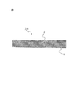
以下、本発明に係るステルスダイシング用粘着シートについて、図面を参照しながら、具体的に説明する。図1に示すように、本発明に係るステルスダイシング用粘着シート10は、基材1と、その片面に形成された粘着剤層2とからなる。
Hereinafter, the stealth dicing pressure-sensitive adhesive sheet according to the present invention will be specifically described with reference to the drawings. As shown in FIG. 1, the
ステルスダイシング用粘着シート10の23℃におけるヤング率は、200〜600MPaであり、好ましくは250〜500MPa、さらに好ましくは300〜400MPaである。
The Young's modulus at 23 ° C. of the stealth dicing pressure-sensitive
また、粘着剤層2の23℃における貯蔵弾性率は、0.10〜50MPaであり、好ましくは0.20〜40MPa、さらに好ましくは1.0〜30MPaである。
Moreover, the storage elastic modulus in 23 degreeC of the
半導体ウエハ11の内部に集光点を合わせてレーザー光が照射され、回路間を区画する仮想的な切断予定ライン18に沿ってウエハ内部に改質部が形成される。次いで、半導体ウエハ11はステルスダイシング用粘着シート10の粘着剤層2に貼付される。その後、粘着シート10はエキスパンドされ、半導体ウエハ11はチップ化(ダイシング)される。粘着シート10及び粘着剤層2の物性が上記範囲にあることで、エキスパンド工程において粘着シート10を均一に延伸させることができ、また、粘着剤層2に貼付された半導体ウエハ11や半導体チップ12が脱落することはない。さらにまた、粘着シート10をエキスパンドする際の応力(エキスパンド力)がウエハ内部の改質部に充分に伝達するため、半導体ウエハ11を歩留まりよくチップ化することができる。
The semiconductor wafer 11 is irradiated with laser light with the focusing point aligned, and a modified portion is formed inside the wafer along a
200mm/分で延伸したときの粘着シート10の破断伸度は、好ましくは50%以上、さらに好ましくは70%以上、特に好ましくは100%以上である。
The breaking elongation of the pressure-sensitive
粘着シート10の破断伸度が上記範囲にあることで、エキスパンドの際に粘着シート10が破断しにくく、チップ同士を離間しやすくなる。
When the elongation at break of the pressure-sensitive
なお、粘着シート10の粘着剤層2を、後述するエネルギー線硬化型粘着剤で形成した場合には、エネルギー線照射の前後で、粘着シートのヤング率、粘着剤層の弾性率、粘着シートの破断伸度が変化する場合がある。エキスパンド工程は、通常、エネルギー線照射前に行うが、エネルギー線照射後に行われることもある。したがって、本発明において規定する粘着シートのヤング率、粘着剤層の弾性率、粘着シートの破断伸度は、通常、エネルギー線照射前の物性値であるが、エネルギー線照射後に上記物性値を満足する粘着シートも本発明の範囲に含まれる。また、特にエキスパンド工程において上記物性値を満足することが好ましい。
When the pressure-sensitive
このようなステルスダイシング用粘着シート10は、図1に示すように、たとえば基材1の片面に粘着剤層2を形成して得られる。基材1としては、例えば、高密度ポリエチレン(HDPE)フィルム等のポリエチレンフィルム、延伸若しくは無延伸のポリプロピレンフィルム、ポリブテンフィルム、ポリブタジエンフィルム、ポリメチルペンテンフィルム、ポリ塩化ビニルフィルム、塩化ビニル共重合体フィルム、ポリウレタンフィルム、エチレン酢酸ビニル共重合体フィルム、およびその水添加物または変性物等からなるフィルムが用いられる。またこれらの架橋フィルム、共重合体フィルムも用いられ、中でもエキスパンド性を考慮すると、ポリ塩化ビニルフィルムが好ましい。上記の基材は1種単独でもよいし、さらにこれらを2種類以上組み合わせた複合フィルムであってもよい。
Such a stealth dicing pressure-sensitive
また、後述するように、粘着剤層2を紫外線硬化型粘着剤で形成し、粘着剤を硬化するために照射するエネルギー線として紫外線を用いる場合には、紫外線に対して透明である基材が好ましい。なお、エネルギー線として電子線を用いる場合には透明である必要はない。上記のフィルムの他、これらを着色した透明フィルム、不透明フィルム等を用いることができる。
As will be described later, when the pressure-sensitive
また、基材1の上面、すなわち粘着剤層2が設けられる側の基材表面には粘着剤との密着性を向上するために、コロナ処理を施したり、プライマー層を設けてもよい。また、粘着剤層2とは反対面に各種の塗膜を塗工してもよい。粘着シート10は、上記のような基材上に粘着剤層を設けることで製造される。基材1の厚みは、好ましくは40〜90μm、さらに好ましくは50〜80μmの範囲にある。このような基材1を用いることにより、エキスパンド力をウエハ内部の改質部にさらに良好に伝達することができる。
Moreover, in order to improve adhesiveness with an adhesive, the upper surface of the
粘着剤層2は、従来より公知の種々の粘着剤により形成され得る。このような粘着剤としては、何ら限定されるものではないが、例えば、ゴム系、アクリル系、シリコーン系、ポリビニルエーテル等の粘着剤が用いられる。また、エネルギー線硬化型や加熱発泡型、水膨潤型の粘着剤も用いることができる。エネルギー線硬化(紫外線硬化、電子線硬化等)型粘着剤としては、特に紫外線硬化型粘着剤を用いることが好ましい。
The pressure-
粘着剤層2をエネルギー線硬化型粘着剤で形成する場合、エネルギー線硬化型粘着成分と必要に応じ光重合開始剤とを配合した粘着剤組成物を用いて、粘着剤層を形成する。さらに、上記粘着剤組成物には、各種物性を改良するため、必要に応じ、その他の成分(架橋剤等)が含まれていてもよい。架橋剤としては、有機多価イソシアナート化合物、有機多価エポキシ化合物、有機多価イミン化合物等があげられる。以下、エネルギー線硬化型粘着成分について、アクリル系粘着剤を例として具体的に説明する。
When forming the pressure-
エネルギー線硬化型粘着成分は、粘着剤組成物に十分な粘着性および造膜性(シート加工性)を付与するためにアクリル重合体(A)を含有し、またエネルギー線硬化性化合物(B)を含有する。エネルギー線硬化性化合物(B)は、またエネルギー線重合性基を含み、紫外線、電子線等のエネルギー線の照射を受けると重合硬化し、粘着剤組成物の粘着力を低下させる機能を有する。また、上記成分(A)および(B)の性質を兼ね備えるものとして、主鎖または側鎖に、エネルギー線重合性基が結合されてなるエネルギー線硬化型粘着性重合体(以下、成分(AB)と記載する場合がある)を用いてもよい。このようなエネルギー線硬化型粘着性重合体(AB)は、粘着性とエネルギー線硬化性とを兼ね備える性質を有する。 The energy ray-curable pressure-sensitive adhesive component contains an acrylic polymer (A) in order to impart sufficient pressure-sensitive adhesiveness and film-forming property (sheet processability) to the pressure-sensitive adhesive composition, and energy ray-curable compound (B). Containing. The energy ray-curable compound (B) also contains an energy ray-polymerizable group, has a function of being polymerized and cured when irradiated with energy rays such as ultraviolet rays and electron beams, and reducing the adhesive strength of the pressure-sensitive adhesive composition. Moreover, as what has the property of said component (A) and (B), the energy-beam curable adhesive polymer (henceforth component (AB)) by which an energy-beam polymeric group is couple | bonded with the principal chain or the side chain. May be used). Such an energy ray curable pressure-sensitive adhesive polymer (AB) has a property having both adhesiveness and energy ray curable properties.
アクリル重合体(A)としては、従来公知のアクリル重合体を用いることができる。アクリル重合体(A)の重量平均分子量(Mw)は、10万〜200万であることが好ましく、30万〜150万であることがより好ましい。また、分子量分布(Mw/Mn、Mnは数平均分子量)は1.0〜10であることが好ましく、1.0〜3.0であることがより好ましい。また、アクリル重合体(A)のガラス転移温度(Tg)は、好ましくは−70〜30℃、さらに好ましくは−60〜20℃の範囲にある。 A conventionally well-known acrylic polymer can be used as an acrylic polymer (A). The weight average molecular weight (Mw) of the acrylic polymer (A) is preferably 100,000 to 2,000,000, and more preferably 300,000 to 1,500,000. Moreover, it is preferable that molecular weight distribution (Mw / Mn, Mn is a number average molecular weight) is 1.0-10, and it is more preferable that it is 1.0-3.0. The glass transition temperature (Tg) of the acrylic polymer (A) is preferably in the range of −70 to 30 ° C., more preferably in the range of −60 to 20 ° C.
上記アクリル重合体(A)を構成するモノマーとしては、(メタ)アクリル酸エステルモノマーまたはその誘導体が挙げられる。例えば、アルキル基の炭素数が1〜18であるアルキル(メタ)アクリレート、例えばメチル(メタ)アクリレート、エチル(メタ)アクリレート、プロピル(メタ)アクリレート、ブチル(メタ)アクリレート、2−エチルヘキシル(メタ)アクリレートなどが挙げられ;環状骨格を有する(メタ)アクリレート、例えばシクロアルキル(メタ)アクリレート、ベンジル(メタ)アクリレート、イソボルニルアクリレート、ジシクロペンタニルアクリレート、ジシクロペンテニルアクリレート、ジシクロペンテニルオキシエチルアクリレート、イミドアクリレートなどが挙げられ;水酸基を有する2−ヒドロキシエチル(メタ)アクリレート、2−ヒドロキシプロピル(メタ)アクリレートなどが挙げられ、アクリル酸、メタクリル酸、イタコン酸、グリシジルメタクリレート、グリシジルアクリレートなどが挙げられる。また、上記アクリル重合体(A)は、酢酸ビニル、アクリロニトリル、スチレン、ビニルアセテートなどが共重合されたアクリル共重合体であることが好ましい。 As a monomer which comprises the said acrylic polymer (A), a (meth) acrylic acid ester monomer or its derivative (s) is mentioned. For example, an alkyl (meth) acrylate having an alkyl group having 1 to 18 carbon atoms, such as methyl (meth) acrylate, ethyl (meth) acrylate, propyl (meth) acrylate, butyl (meth) acrylate, 2-ethylhexyl (meth) Acrylates and the like; (meth) acrylates having a cyclic skeleton such as cycloalkyl (meth) acrylate, benzyl (meth) acrylate, isobornyl acrylate, dicyclopentanyl acrylate, dicyclopentenyl acrylate, dicyclopentenyloxyethyl Acrylate, imide acrylate, etc .; 2-hydroxyethyl (meth) acrylate having a hydroxyl group, 2-hydroxypropyl (meth) acrylate, etc., acrylic acid, methacrylic acid, Con acid, glycidyl methacrylate, and glycidyl acrylate. The acrylic polymer (A) is preferably an acrylic copolymer obtained by copolymerizing vinyl acetate, acrylonitrile, styrene, vinyl acetate or the like.
エネルギー線硬化性化合物(B)は、紫外線、電子線等のエネルギー線の照射を受けると重合硬化する化合物である。このエネルギー線重合性化合物の例としては、エネルギー線重合性基を有する低分子量化合物(単官能、多官能のモノマーおよびオリゴマー)があげられ、具体的には、トリメチロールプロパントリアクリレート、テトラメチロールメタンテトラアクリレート、ペンタエリスリトールトリアクリレート、ジペンタエリスリトールモノヒドロキシペンタアクリレート、ジペンタエリスリトールヘキサアクリレートあるいは1,4−ブチレングリコールジアクリレート、1,6−ヘキサンジオールジアクリレート、ジシクロペンタジエンジメトキシジアクリレート、イソボルニルアクリレートなどの環状脂肪族骨格含有アクリレート、ポリエチレングリコールジアクリレート、オリゴエステルアクリレート、ウレタンアクリレートオリゴマー、エポキシ変性アクリレート、ポリエーテルアクリレート、イタコン酸オリゴマーなどのアクリレート系化合物が用いられる。このような化合物は、分子内に少なくとも1つの重合性二重結合を有し、通常は、分子量が100〜30000、好ましくは300〜10000程度である。 The energy ray curable compound (B) is a compound that is polymerized and cured when irradiated with energy rays such as ultraviolet rays and electron beams. Examples of the energy beam polymerizable compound include low molecular weight compounds (monofunctional and polyfunctional monomers and oligomers) having an energy beam polymerizable group, and specifically include trimethylolpropane triacrylate and tetramethylolmethane. Tetraacrylate, pentaerythritol triacrylate, dipentaerythritol monohydroxypentaacrylate, dipentaerythritol hexaacrylate or 1,4-butylene glycol diacrylate, 1,6-hexanediol diacrylate, dicyclopentadiene dimethoxydiacrylate, isobornyl Cyclic aliphatic skeleton-containing acrylate such as acrylate, polyethylene glycol diacrylate, oligoester acrylate, urethane acrylate oligomer, Carboxy-modified acrylates, polyether acrylates, acrylate compounds such as itaconic acid oligomer is used. Such a compound has at least one polymerizable double bond in the molecule, and usually has a molecular weight of about 100 to 30,000, preferably about 300 to 10,000.
一般的には成分(A)100重量部に対して、成分(B)は10〜400重量部、好ましくは30〜350重量部程度の割合で用いられる。 Generally, the component (B) is used in a proportion of 10 to 400 parts by weight, preferably about 30 to 350 parts by weight, relative to 100 parts by weight of the component (A).
上記成分(A)および(B)の性質を兼ね備えるエネルギー線硬化型粘着性重合体(AB)は、主鎖または側鎖に、エネルギー線重合性基が結合されてなる。 The energy ray-curable pressure-sensitive adhesive polymer (AB) having the properties of the components (A) and (B) has an energy ray polymerizable group bonded to the main chain or side chain.
エネルギー線硬化型粘着性重合体の主骨格は特に限定はされず、粘着剤として汎用されているアクリル共重合体であってもよく、またエステル型、エーテル型の何れであっても良いが、合成および粘着物性の制御が容易であることから、アクリル共重合体を主骨格とすることが特に好ましい。 The main skeleton of the energy ray curable adhesive polymer is not particularly limited, and may be an acrylic copolymer widely used as an adhesive, and may be either an ester type or an ether type, It is particularly preferable to use an acrylic copolymer as the main skeleton because synthesis and control of adhesive properties are easy.
エネルギー線硬化型粘着性重合体の主鎖または側鎖に結合するエネルギー線重合性基は、たとえばエネルギー線重合性の炭素−炭素二重結合を含む基であり、具体的には(メタ)アクリロイル基等を例示することができる。エネルギー線重合性基は、アルキレン基、アルキレンオキシ基、ポリアルキレンオキシ基を介してエネルギー線硬化型粘着性重合体に結合していてもよい。 The energy beam polymerizable group bonded to the main chain or side chain of the energy beam curable adhesive polymer is, for example, a group containing an energy beam polymerizable carbon-carbon double bond, and specifically, (meth) acryloyl. Examples include groups. The energy beam polymerizable group may be bonded to the energy beam curable pressure-sensitive adhesive polymer via an alkylene group, an alkyleneoxy group, or a polyalkyleneoxy group.
エネルギー線重合性基が結合されたエネルギー線硬化型粘着性重合体(AB)の重量平均分子量(Mw)は、10万〜200万であることが好ましく、30万〜150万であることがより好ましい。また、分子量分布(Mw/Mn、Mnは数平均分子量)は1.0〜10であることが好ましく、1.0〜3.0であることがより好ましい。また、エネルギー線硬化型粘着性重合体(AB)のガラス転移温度(Tg)は、好ましくは−70〜30℃、より好ましくは−60〜20℃の範囲にある。 The weight average molecular weight (Mw) of the energy beam curable adhesive polymer (AB) to which the energy beam polymerizable group is bonded is preferably 100,000 to 2,000,000, more preferably 300,000 to 1,500,000. preferable. Moreover, it is preferable that molecular weight distribution (Mw / Mn, Mn is a number average molecular weight) is 1.0-10, and it is more preferable that it is 1.0-3.0. The glass transition temperature (Tg) of the energy ray curable adhesive polymer (AB) is preferably in the range of −70 to 30 ° C., more preferably in the range of −60 to 20 ° C.
エネルギー線硬化型粘着性重合体(AB)は、例えば、ヒドロキシル基、カルボキシル基、アミノ基、置換アミノ基、エポキシ基等の官能基を含有するアクリル粘着性重合体と、該官能基と反応する置換基とエネルギー線重合性炭素−炭素二重結合を1分子毎に1〜5個を有する重合性基含有化合物とを反応させて得られる。アクリル粘着性重合体は、ヒドロキシル基、カルボキシル基、アミノ基、置換アミノ基、エポキシ基等の官能基を有する(メタ)アクリル酸エステルモノマーまたはその誘導体と、前述した成分(A)を構成するモノマーとからなる共重合体であることが好ましい。また、該重合性基含有化合物としては、(メタ)アクリロイルオキシエチルイソシアネート、メタ−イソプロペニル−α,α−ジメチルベンジルイソシアネート、(メタ)アクリロイルイソシアネート、アリルイソシアネート、グリシジル(メタ)アクリレート;(メタ)アクリル酸等が挙げられる。 The energy ray curable adhesive polymer (AB) reacts with the acrylic adhesive polymer containing a functional group such as a hydroxyl group, a carboxyl group, an amino group, a substituted amino group, and an epoxy group, for example, with the functional group. It is obtained by reacting a substituent with a polymerizable group-containing compound having 1 to 5 energy beam polymerizable carbon-carbon double bonds per molecule. Acrylic adhesive polymer is a monomer that comprises (meth) acrylic acid ester monomer or derivative thereof having a functional group such as hydroxyl group, carboxyl group, amino group, substituted amino group, and epoxy group, and component (A) described above. A copolymer consisting of The polymerizable group-containing compound includes (meth) acryloyloxyethyl isocyanate, meta-isopropenyl-α, α-dimethylbenzyl isocyanate, (meth) acryloyl isocyanate, allyl isocyanate, glycidyl (meth) acrylate; Acrylic acid etc. are mentioned.
上記のようなアクリル重合体(A)およびエネルギー線硬化性化合物(B)又は、エネルギー線硬化型粘着性重合体(AB)を含むエネルギー線硬化型粘着成分は、エネルギー線照射により硬化する。エネルギー線としては、具体的には、紫外線、電子線等が用いられる。 The energy ray curable adhesive component containing the acrylic polymer (A) and the energy ray curable compound (B) or the energy ray curable adhesive polymer (AB) as described above is cured by energy ray irradiation. Specifically, ultraviolet rays, electron beams, etc. are used as the energy rays.
光重合開始剤としては、ベンゾイン化合物、アセトフェノン化合物、アシルフォスフィンオキサイド化合物、チタノセン化合物、チオキサントン化合物、パーオキサイド化合物等の光開始剤、アミンやキノン等の光増感剤などが挙げられ、具体的には、1−ヒドロキシシクロヘキシルフェニルケトン、ベンゾイン、ベンゾインメチルエーテル、ベンゾインエチルエーテル、ベンゾインイソプロピルエーテル、ベンジルジフェニルサルファイド、テトラメチルチウラムモノサルファイド、アゾビスイソブチロニトリル、ジベンジル、ジアセチル、β−クロールアンスラキノン、2,4,6−トリメチルベンゾイルジフェニルフォスフィンオキサイドなどが例示できる。エネルギー線として紫外線を用いる場合に、光重合開始剤を配合することにより照射時間、照射量を少なくすることができる。 Examples of photopolymerization initiators include photoinitiators such as benzoin compounds, acetophenone compounds, acylphosphine oxide compounds, titanocene compounds, thioxanthone compounds, and peroxide compounds, and photosensitizers such as amines and quinones. 1-hydroxycyclohexyl phenyl ketone, benzoin, benzoin methyl ether, benzoin ethyl ether, benzoin isopropyl ether, benzyl diphenyl sulfide, tetramethyl thiuram monosulfide, azobisisobutyronitrile, dibenzyl, diacetyl, β-chloranthraquinone Examples include 2,4,6-trimethylbenzoyldiphenylphosphine oxide. When ultraviolet rays are used as energy rays, the irradiation time and irradiation amount can be reduced by adding a photopolymerization initiator.
粘着剤層2の厚みは、好ましくは1〜15μm、さらに好ましくは2〜10μm、特に好ましくは3〜8μmの範囲である。
The thickness of the pressure-
また、粘着剤層2には、その使用前に粘着剤層を保護するために剥離シートが積層されていてもよい。剥離シートは、特に限定されるものではなく、例えば、ポリエチレンテレフタレート、ポリプロピレン、ポリエチレン等の樹脂からなるフィルムまたはそれらの発泡フィルムや、グラシン紙、コート紙、ラミネート紙等の紙に、シリコーン系、フッ素系、長鎖アルキル基含有カルバメート等の剥離剤で剥離処理したものを使用することができる。
In addition, a release sheet may be laminated on the pressure-
基材1の表面に粘着剤層2を設ける方法は、剥離シート上に所定の膜厚になるように塗布し形成した粘着剤層2を基材1の表面に転写しても構わないし、基材1の表面に直接塗布して粘着剤層2を形成しても構わない。
The method of providing the pressure-
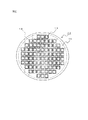
次に、本発明に係る粘着シート10を用いる半導体装置の製造方法について説明する。本発明に係る半導体装置の製造方法について、表面に回路13が形成された半導体ウエハ11をチップ化する場合を例にとり説明する。図2に、表面に回路13が形成された半導体ウエハ11の回路面側の平面図を示す。なお、切断予定ライン18は、各回路13間を区画する仮想的なラインである。
Next, a method for manufacturing a semiconductor device using the pressure-
半導体ウエハ11はシリコンウエハであってもよく、またガリウム・砒素などの化合物半導体ウエハであってもよい。ウエハ表面への回路13の形成はエッチング法、リフトオフ法などの従来より汎用されている方法を含む様々な方法により行うことができる。半導体ウエハの回路形成工程において、所定の回路13が形成される。回路13は、ウエハ11の内周部14表面に格子状に形成される。ウエハ11の研削前の厚みは特に限定されないが、通常は500〜1000μm程度である。
The semiconductor wafer 11 may be a silicon wafer or a compound semiconductor wafer such as gallium / arsenic. The formation of the
裏面研削時には、表面の回路13を保護するために回路面に、表面保護シートと呼ばれる粘着シートを貼付する。裏面研削は、ウエハ11の回路面側(すなわち表面保護シート側)をチャックテーブル等により固定し、回路13が形成されていない裏面側をグラインダーにより研削する。この結果、研削後の半導体ウエハ11の厚みは特に限定されないが、通常50〜200μm程度になる。裏面研削工程の後、研削によってウエハ裏面に生成した破砕層を除去する工程が行われてもよい。
At the time of back grinding, an adhesive sheet called a surface protective sheet is attached to the circuit surface in order to protect the
裏面研削工程に続いて、必要に応じ裏面にエッチング処理などの発熱を伴う加工処理や、裏面への金属膜の蒸着、有機膜の焼き付けのように高温で行われる処理を施してもよい。なお、高温での処理を行う場合には、通常、表面保護シートを剥離した後に、裏面への処理を行う。 Subsequent to the back grinding step, if necessary, the back surface may be subjected to processing that generates heat such as an etching process, or processing performed at a high temperature such as vapor deposition of a metal film or baking of an organic film on the back surface. In addition, when processing at high temperature, the process to a back surface is normally performed after peeling a surface protection sheet.
裏面研削後、ウエハ11の裏面側からウエハ11内部にレーザー光を照射する。レーザー光はレーザー光源より照射される。レーザー光源は、波長及び位相が揃った光を発生させる装置であり、レーザー光の種類としては、パルスレーザー光を発生するNd−YAGレーザー、Nd−YVOレーザー、Nd−YLFレーザー、チタンサファイアレーザーなど多光子吸収を起こすものを挙げることができる。レーザー光の波長は、800〜1100nmが好ましく、1064nmがさらに好ましい。 After the back surface grinding, laser light is irradiated into the wafer 11 from the back surface side of the wafer 11. Laser light is emitted from a laser light source. The laser light source is a device that generates light having a uniform wavelength and phase, and the types of laser light include Nd-YAG laser, Nd-YVO laser, Nd-YLF laser, and titanium sapphire laser that generate pulsed laser light. The thing which causes multiphoton absorption can be mentioned. The wavelength of the laser light is preferably 800 to 1100 nm, and more preferably 1064 nm.
レーザー光はウエハ内部に照射され、切断予定ライン18に沿ってウエハ内部に改質部が形成される。ひとつの切断予定ラインをレーザー光が走査する回数は1回であっても複数回であってもよい。好ましくは、レーザー光の照射位置と、回路間の切断予定ライン18の位置をモニターし、レーザー光の位置合わせを行いながら、レーザー光の照射を行う。
The laser beam is irradiated inside the wafer, and a modified portion is formed inside the wafer along the scheduled cutting
改質部形成後、図3に示すように、ウエハ11の裏面に本発明に係るステルスダイシング用粘着シート10の粘着剤層2を貼付し、ウエハ11のダイシングを行う。なお、表面保護シートがウエハ表面に貼付されている場合には、粘着シート10の貼付前または貼付後に表面保護シートを剥離する。粘着シート10のウエハ裏面への貼付は、マウンターと呼ばれる装置により行われるのが一般的だが特に限定はされない。
After forming the modified portion, as shown in FIG. 3, the
レーザー光照射によりウエハ内部に改質部を形成した後、エキスパンドを行うと、粘着シート10は伸長し、半導体ウエハ11は、ウエハ内部の改質部を起点として個々のチップ12に切断分離される。また、エキスパンドと同時に粘着シート10を基材1側から治具等を用いてひっかくようにして、粘着シート10を伸長しウエハ11をチップ12に切断分離することもできる。エキスパンドは、5〜600mm/分の速度で行うことが好ましい。その後、チップ12はピックアップされ、ボンディング工程を経て半導体装置が製造される。なお、粘着剤層2をエネルギー線硬化型粘着剤で形成した場合は、ピックアップ工程の前にエネルギー線を照射することが好ましい。
When the expanded portion is formed after forming the modified portion inside the wafer by laser light irradiation, the
以上、本発明のステルスダイシング用粘着シート10の使用例について説明したが、本発明のステルスダイシング用粘着シート10は、通常の半導体ウエハ、ガラス基板、セラミック基板、FPC等の有機材料基板、又は精密部品等の金属材料などの種々の物品のダイシングに使用することができる。
As mentioned above, although the usage example of the
以下本発明を実施例により説明するが、本発明はこれら実施例に限定されるものではない。 EXAMPLES The present invention will be described below with reference to examples, but the present invention is not limited to these examples.
<ステルスダイシング条件>
下記シリコンウエハの裏面側から、シリコンウエハ内部に下記の条件でレーザー光を照射した。次いで、シリコンウエハ裏面に実施例又は比較例の粘着シートを貼付し、リングフレームに固定した。その後、粘着シートをエキスパンドし、シリコンウエハをチップ化した。なお、カットチップサイズは、2mm×2mm、0.5mm×0.5mm、0.15mm×0.15mmとした。また、粘着シートの粘着剤層にエネルギー線硬化型の粘着剤層を用いる場合は、エネルギー線照射前に粘着シートをエキスパンドした。
・装置 :Nd−YAGレーザー
・波長 :1064nm
・繰り返し周波数 :100kHz
・パルス幅 :30nm
・カット速度 :100mm/秒
・ウエハ材質 :シリコン
・ウエハ厚 :100μm
・ウエハサイズ :50mm×50mm(正方形)
・粘着シートサイズ :約207mmφ
<Stealth dicing conditions>
Laser light was irradiated from the back side of the following silicon wafer into the silicon wafer under the following conditions. Subsequently, the adhesive sheet of the Example or the comparative example was stuck on the back surface of the silicon wafer and fixed to the ring frame. Thereafter, the adhesive sheet was expanded to form a silicon wafer as a chip. The cut chip size was 2 mm × 2 mm, 0.5 mm × 0.5 mm, and 0.15 mm × 0.15 mm. Moreover, when using an energy ray hardening-type adhesive layer for the adhesive layer of an adhesive sheet, the adhesive sheet was expanded before energy ray irradiation.
-Equipment: Nd-YAG laser-Wavelength: 1064 nm
・ Repetition frequency: 100 kHz
・ Pulse width: 30 nm
・ Cut speed: 100 mm / second ・ Wafer material: Silicon ・ Wafer thickness: 100 μm
-Wafer size: 50mm x 50mm (square)
・ Adhesive sheet size: Approximately 207mmφ
<粘着シートのヤング率、破断伸度>
粘着シートのヤング率及び破断伸度は、万能引張試験機(オリエンテック社製テンシロンRTA−T−2M)を用いて、JIS K7161:1994に準拠して、23℃、湿度50%の環境下において引張速度200mm/分で測定した。なお、粘着シートの粘着剤層にエネルギー線硬化型の粘着剤層を用いる場合は、エネルギー線照射前の粘着シートのヤング率及び破断伸度を測定した。
<Young's modulus of adhesive sheet, elongation at break>
The Young's modulus and elongation at break of the pressure-sensitive adhesive sheet were measured in an environment of 23 ° C. and 50% humidity in accordance with JIS K7161: 1994 using a universal tensile tester (Tensilon RTA-T-2M manufactured by Orientec Corp.). Measurement was performed at a pulling speed of 200 mm / min. In addition, when using an energy ray hardening-type adhesive layer for the adhesive layer of an adhesive sheet, the Young's modulus and breaking elongation of the adhesive sheet before energy ray irradiation were measured.
<粘着剤層の貯蔵弾性率(G’)>
実施例および比較例について、シリコーン剥離処理を行った2枚のポリエチレンテレフタレートフィルム(剥離フィルム)で挟まれた粘着剤層を得た。片方の剥離フィルムを剥がし、粘着剤層が重なるように積層を繰り返し、厚みが3mmの粘着剤層を得た。直径8mmの円柱形に型抜きして弾性率測定用の試料を作製した。両側の剥離フィルムを剥がし、この試料の捻り剪断法による周波数1Hz、温度23℃における貯蔵弾性率(G’)を、粘弾性測定装置(RHEOMETRIC社製DYNAMIC ANALYZER RDA−II)を用いて測定した。なお、エネルギー線硬化型の粘着剤層を用いる場合は、エネルギー線照射前の粘着剤層の貯蔵弾性率(G’)を測定した。
<Storage elastic modulus of adhesive layer (G ')>
About the Example and the comparative example, the adhesive layer pinched | interposed by the two polyethylene terephthalate films (peeling film) which performed the silicone peeling process was obtained. One release film was peeled off and the lamination was repeated so that the pressure-sensitive adhesive layers overlapped to obtain a pressure-sensitive adhesive layer having a thickness of 3 mm. A sample for elastic modulus measurement was produced by punching into a cylindrical shape with a diameter of 8 mm. The release films on both sides were peeled, and the storage elastic modulus (G ′) at a frequency of 1 Hz and a temperature of 23 ° C. was measured using a viscoelasticity measuring apparatus (DYNAMIC ANALYZER RDA-II manufactured by RHEOMETRIC). In addition, when using an energy ray hardening-type adhesive layer, the storage elastic modulus (G ') of the adhesive layer before energy ray irradiation was measured.
<基材及び粘着剤層の厚さ>
基材及び粘着剤層の厚さは、定圧厚さ計(TECLOCK製PG−02)を用いて測定した。
<Thickness of base material and pressure-sensitive adhesive layer>
The thickness of the base material and the pressure-sensitive adhesive layer was measured using a constant pressure thickness meter (PG-02 manufactured by TECLOCK).
<粘着シートのエキスパンド性>
8インチウエハ用のリングフレームに実施例又は比較例の粘着シートを貼付し、エキスパンド装置(ディスコ社製、DDS2010)を用い、300mm/分でエキスパンド(10mm引き落とし)した。問題なくエキスパンドできた場合を「良好」とし、リングフレームから粘着シートが脱落したり、粘着シートが裂けてしまった場合を「不良」とした。なお、粘着シートの粘着剤層にエネルギー線硬化型の粘着剤層を用いる場合は、エネルギー線照射前の粘着シートのエキスパンド性を評価した。
<Expandability of adhesive sheet>
The pressure-sensitive adhesive sheet of Example or Comparative Example was attached to a ring frame for an 8-inch wafer, and expanded (drawn 10 mm) at 300 mm / min using an expanding device (DDS 2010, manufactured by Disco Corporation). The case where it was able to expand without problems was defined as “good”, and the case where the adhesive sheet dropped from the ring frame or the adhesive sheet was torn was regarded as “bad”. In addition, when using an energy ray hardening-type adhesive layer for the adhesive layer of an adhesive sheet, the expandability of the adhesive sheet before energy ray irradiation was evaluated.
<チップ分割率>
上記のステルスダイシング条件で、シリコンウエハの内部に改質部を形成し、ウエハと8インチウエハ用リングフレームとを実施例又は比較例の粘着シートに貼付後、エキスパンド装置(ディスコ社製、DDS2010)を用いて、粘着シートをエキスパンドし、ウエハをチップ化した。なお、カットチップサイズが2mm×2mmのものは、粘着シートをエキスパンド(300mm/分で10mm引き落とし)してウエハをチップ化し、カットチップサイズが0.5mm×0.5mm及び0.15mm×0.15mmのものは、エキスパンド(300mm/分で5mm引き落とし)と同時に粘着シートを基材側から治具を用いてひっかいて、ウエハをチップ化した。カットチップサイズにチップ化されたチップの数(完全に個片化されたチップの数)を目視にて数え、ウエハ上に想定された全チップ数(仮想チップの合計数)に対するチップ分割率を算出した。チップ分割率が99.5%以上の場合を「非常に良好」、98%以上を「良好」、98%未満を「不良」とした。また、粘着シートの粘着剤層にエネルギー線硬化型の粘着剤層を用いる場合は、エネルギー線照射前に粘着シートをエキスパンドした。
<Chip division ratio>
Under the above stealth dicing conditions, a modified portion is formed inside the silicon wafer, and the wafer and an 8-inch wafer ring frame are attached to the adhesive sheet of the example or the comparative example, and then an expanding apparatus (DDS 2010, manufactured by DISCO Corporation) Was used to expand the adhesive sheet, and the wafer was chipped. When the cut chip size is 2 mm × 2 mm, the adhesive sheet is expanded (drawn 10 mm at 300 mm / min) to chip the wafer, and the cut chip sizes are 0.5 mm × 0.5 mm and 0.15 mm × 0. In the case of 15 mm, the adhesive sheet was scratched from the base material side with a jig at the same time as the expansion (drawn 5 mm at 300 mm / min), and the wafer was chipped. Visually count the number of chips cut to the cut chip size (the number of chips completely separated), and calculate the chip division ratio for the total number of chips (total number of virtual chips) assumed on the wafer Calculated. When the chip division ratio was 99.5% or more, it was determined as “very good”, 98% or more as “good”, and less than 98% as “bad”. Moreover, when using an energy ray hardening-type adhesive layer for the adhesive layer of an adhesive sheet, the adhesive sheet was expanded before energy ray irradiation.
(実施例1)
アクリル共重合体(2−エチルヘキシルアクリレート/酢酸ビニル/アクリル酸/メチルメタクリレート/2−ヒドロキシエチルメタクリレート=18.5/75/1/5/0.5(質量比)、Mw=60万、Mw/Mn=8.2、Tg=5℃)100重量部に対し、エネルギー線硬化性化合物として2官能ウレタンアクリレートオリゴマー(Mw=8000)60重量部、6官能ウレタンアクリレートオリゴマー(Mw=2000)60重量部を配合したエネルギー線硬化型粘着成分に、光重合開始剤(チバ・スペシャルティ・ケミカルズ社製「イルガキュア184」)3重量部及び多価イソシアナート化合物(日本ポリウレタン社製、コロネートL)3重量部を配合(すべて固形分換算による配合比)し、粘着剤組成物とした。
Example 1
Acrylic copolymer (2-ethylhexyl acrylate / vinyl acetate / acrylic acid / methyl methacrylate / 2-hydroxyethyl methacrylate = 18.5 / 75/1/5 / 0.5 (mass ratio), Mw = 600,000, Mw / 100 parts by weight of Mn = 8.2, Tg = 5 ° C.) 60 parts by weight of bifunctional urethane acrylate oligomer (Mw = 8000), 60 parts by weight of hexafunctional urethane acrylate oligomer (Mw = 2000) as an energy ray
剥離フィルムに、上記粘着剤組成物を塗布した後に、乾燥(オーブンにて100℃、1分間)させ、厚み10μmの粘着剤層を作製した。次いで、基材として、厚さ80μmのポリ塩化ビニルフィルム(ヤング率=350MPa)を用い、粘着剤層を転写し、ステルスダイシング用粘着シートを得た。この粘着シートについて、「粘着シートのヤング率、破断伸度」及び「粘着剤層の貯蔵弾性率(G’)」を測定し、「粘着シートのエキスパンド性」及び「チップ分割率」を評価した。結果を表1に示す。 After apply | coating the said adhesive composition to a peeling film, it was made to dry (100 degreeC and 1 minute in oven), and the 10-micrometer-thick adhesive layer was produced. Next, a 80 μm-thick polyvinyl chloride film (Young's modulus = 350 MPa) was used as a base material, and the pressure-sensitive adhesive layer was transferred to obtain an adhesive sheet for stealth dicing. About this pressure-sensitive adhesive sheet, “Young's modulus and elongation at break of pressure-sensitive adhesive sheet” and “Storage elastic modulus (G ′) of pressure-sensitive adhesive layer” were measured, and “Expandability of pressure-sensitive adhesive sheet” and “Chip division ratio” were evaluated. . The results are shown in Table 1.
(実施例2)
粘着剤層の厚みを5μmとした以外は、実施例1と同様にしてステルスダイシング用粘着シートを得、測定及び評価を行った。結果を表1に示す。
(Example 2)
A stealth dicing pressure-sensitive adhesive sheet was obtained in the same manner as in Example 1 except that the thickness of the pressure-sensitive adhesive layer was 5 μm, and measurement and evaluation were performed. The results are shown in Table 1.
(実施例3)
基材として、厚さ80μmの無延伸ポリプロピレンフィルム(ヤング率=550MPa)を用いた以外は、実施例1と同様にしてステルスダイシング用粘着シートを得、測定及び評価を行った。結果を表1に示す。
(Example 3)
A stealth dicing adhesive sheet was obtained, measured and evaluated in the same manner as in Example 1 except that an unstretched polypropylene film having a thickness of 80 μm (Young's modulus = 550 MPa) was used as the substrate. The results are shown in Table 1.
(実施例4)
アクリル粘着性重合体(ブチルアクリレート/メチルメタクリレート/2−ヒドロキシエチルアクリレート=62/10/28(質量比))100重量部に対して、重合性基含有化合物としてメタクリロイルオキシエチルイソシアネート30重量部を反応させたエネルギー線硬化型粘着性重合体(Mw=55万、Mw/Mn=6.2、Tg=−30℃)に、光重合開始剤(チバ・スペシャルティ・ケミカルズ社製「イルガキュア184」)2.5重量部及び多価イソシアナート化合物(日本ポリウレタン社製、コロネートL)1.1重量部を配合(すべて固形分換算による配合比)し、粘着剤組成物とした以外は、実施例1と同様にしてステルスダイシング用粘着シートを得、測定及び評価を行った。結果を表1に示す。
Example 4
100 parts by weight of acrylic adhesive polymer (butyl acrylate / methyl methacrylate / 2-hydroxyethyl acrylate = 62/10/28 (mass ratio)) is reacted with 30 parts by weight of methacryloyloxyethyl isocyanate as a polymerizable group-containing compound. A photopolymerization initiator (“Irgacure 184” manufactured by Ciba Specialty Chemicals Co., Ltd.) 2 to the energy ray curable adhesive polymer (Mw = 550,000, Mw / Mn = 6.2, Tg = −30 ° C.) 2 Example 1 except that 1.5 parts by weight and 1.1 parts by weight of a polyvalent isocyanate compound (manufactured by Nippon Polyurethane Co., Ltd., Coronate L) were blended (all blending ratios in terms of solid content) to obtain a pressure-sensitive adhesive composition. Similarly, an adhesive sheet for stealth dicing was obtained and measured and evaluated. The results are shown in Table 1.
(実施例5)
粘着剤層の厚みを5μmとした以外は、実施例4と同様にしてステルスダイシング用粘着シートを得、測定及び評価を行った。結果を表1に示す。
(Example 5)
A stealth dicing pressure-sensitive adhesive sheet was obtained in the same manner as in Example 4 except that the thickness of the pressure-sensitive adhesive layer was 5 μm, and measurement and evaluation were performed. The results are shown in Table 1.
(実施例6)
アクリル共重合体(東レコーテックス製アクリルラバー S−9000、Mw=60万、Mw/Mn=2.4、Tg=−25℃)100重量部に対し、多価イソシアナート化合物(日本ポリウレタン社製、コロネートL)1.9重量部を配合(すべて固形分換算による配合比)し、粘着剤組成物とした。
(Example 6)
To 100 parts by weight of acrylic copolymer (acrylic rubber S-9000, Toray Cortex, Mw = 600,000, Mw / Mn = 2.4, Tg = −25 ° C.), polyvalent isocyanate compound (manufactured by Nippon Polyurethane Co., Ltd.) , Coronate L) 1.9 parts by weight was blended (all blending ratios in terms of solid content) to obtain an adhesive composition.
上記粘着剤組成物を用い、粘着剤層の厚みを5μmとした以外は、実施例1と同様にしてステルスダイシング用粘着シートを得、測定及び評価を行った。結果を表1に示す。 A pressure-sensitive adhesive sheet for stealth dicing was obtained in the same manner as in Example 1 except that the pressure-sensitive adhesive composition was used and the thickness of the pressure-sensitive adhesive layer was 5 μm, and measurement and evaluation were performed. The results are shown in Table 1.
(実施例7)
基材として、厚さ50μmのポリ塩化ビニルフィルム(ヤング率=350MPa)を用いた以外は、実施例2と同様にしてステルスダイシング用粘着シートを得、測定及び評価を行った。結果を表1に示す。
(Example 7)
A stealth dicing adhesive sheet was obtained, measured and evaluated in the same manner as in Example 2 except that a 50 μm-thick polyvinyl chloride film (Young's modulus = 350 MPa) was used as the substrate. The results are shown in Table 1.
(実施例8)
粘着剤層の厚みを15μmとした以外は、実施例1と同様にしてステルスダイシング用粘着シートを得、測定及び評価を行った。結果を表1に示す。
(Example 8)
A stealth dicing pressure-sensitive adhesive sheet was obtained in the same manner as in Example 1 except that the thickness of the pressure-sensitive adhesive layer was 15 μm, and measurement and evaluation were performed. The results are shown in Table 1.
(比較例1)
基材として、厚さ80μmのエチレン・メタクリル酸共重合体フィルム(ヤング率=120MPa)を用いた以外は、実施例1と同様にしてステルスダイシング用粘着シートを得、測定及び評価を行った。結果を表1に示す。
(Comparative Example 1)
A stealth dicing pressure-sensitive adhesive sheet was obtained, measured and evaluated in the same manner as in Example 1 except that an 80 μm thick ethylene / methacrylic acid copolymer film (Young's modulus = 120 MPa) was used as the substrate. The results are shown in Table 1.
(比較例2)
アクリル共重合体(ブチルアクリレート/アクリル酸=91/9(質量比)、Mw=80万、Mw/Mn=10.5、Tg=−38℃)100重量部に対し、エネルギー線硬化性化合物として3官能ウレタンアクリレートオリゴマー(Mw=4000)124重量部を配合したエネルギー線硬化型粘着成分に、光重合開始剤(チバ・スペシャルティ・ケミカルズ社製「イルガキュア184」)3重量部及び多価イソシアナート化合物(日本ポリウレタン社製、コロネートL)2.2重量部を配合(すべて固形分換算による配合比)し、粘着剤組成物とした以外は、実施例1と同様にしてステルスダイシング用粘着シートを得、測定及び評価を行った。結果を表1に示す。
(Comparative Example 2)
As an energy ray curable compound for 100 parts by weight of an acrylic copolymer (butyl acrylate / acrylic acid = 91/9 (mass ratio), Mw = 800,000, Mw / Mn = 10.5, Tg = −38 ° C.) An energy ray-curable adhesive component containing 124 parts by weight of a trifunctional urethane acrylate oligomer (Mw = 4000), 3 parts by weight of a photopolymerization initiator (“Irgacure 184” manufactured by Ciba Specialty Chemicals) and a polyvalent isocyanate compound (Adhesive sheet for stealth dicing was obtained in the same manner as in Example 1 except that 2.2 parts by weight (manufactured by Nippon Polyurethane Co., Ltd., Coronate L) was blended (all blending ratios in terms of solid content) to obtain a pressure-sensitive adhesive composition. Measurement and evaluation were performed. The results are shown in Table 1.
(比較例3)
基材として、厚さ50μmのポリエチレンテレフタレートフィルム(ヤング率=4500MPa)を用いた以外は、実施例1と同様にしてステルスダイシング用粘着シートを得、測定及び評価を行った。結果を表1に示す。
(Comparative Example 3)
A stealth dicing pressure-sensitive adhesive sheet was obtained, measured and evaluated in the same manner as in Example 1 except that a 50 μm-thick polyethylene terephthalate film (Young's modulus = 4500 MPa) was used as the substrate. The results are shown in Table 1.

1…基材
2…粘着剤層
10…ステルスダイシング用粘着シート
11…半導体ウエハ
12…半導体チップ
13…回路
18…切断予定ライン(仮想)
DESCRIPTION OF
Claims (8)
基材と、その片面に形成された粘着剤層とからなり、
該粘着シートの23℃におけるヤング率が200〜600MPaであり、
周波数1Hz、23℃における該粘着剤層の貯蔵弾性率が0.10〜50MPaであるステルスダイシング用粘着シート。 An adhesive sheet for stealth dicing that is used to cut and separate individual chips after forming a modified portion inside a semiconductor wafer,
It consists of a base material and an adhesive layer formed on one side,
The Young's modulus at 23 ° C. of the pressure-sensitive adhesive sheet is 200 to 600 MPa,
The adhesive sheet for stealth dicing whose storage elastic modulus of this adhesive layer in frequency 1Hz and 23 degreeC is 0.10-50 Mpa.
該半導体ウエハの裏面に、請求項1〜7のいずれかに記載のステルスダイシング用粘着シートを貼付する工程、
該粘着シートのエキスパンドにより、該半導体ウエハを分割してチップ化する工程、及び
該半導体チップをピックアップする工程を含む半導体装置の製造方法。
Irradiating a semiconductor wafer having a circuit formed on its surface with laser light to form a modified portion inside the wafer;
Attaching the adhesive sheet for stealth dicing according to any one of claims 1 to 7 to the back surface of the semiconductor wafer;
A method of manufacturing a semiconductor device, comprising: dividing the semiconductor wafer into chips by expanding the adhesive sheet; and picking up the semiconductor chips.
Priority Applications (3)
| Application Number | Priority Date | Filing Date | Title |
|---|---|---|---|
| JP2009276906A JP5128575B2 (en) | 2009-12-04 | 2009-12-04 | Stealth dicing adhesive sheet and method for manufacturing semiconductor device |
| KR1020100122174A KR101215105B1 (en) | 2009-12-04 | 2010-12-02 | An adhesive sheet for a stealth dicing and a production method of a semiconductor wafer device |
| US12/958,446 US8106522B2 (en) | 2009-12-04 | 2010-12-02 | Adhesive sheet for a stealth dicing and a production method of a semiconductor wafer device |
Applications Claiming Priority (1)
| Application Number | Priority Date | Filing Date | Title |
|---|---|---|---|
| JP2009276906A JP5128575B2 (en) | 2009-12-04 | 2009-12-04 | Stealth dicing adhesive sheet and method for manufacturing semiconductor device |
Publications (3)
| Publication Number | Publication Date |
|---|---|
| JP2011119548A JP2011119548A (en) | 2011-06-16 |
| JP2011119548A5 JP2011119548A5 (en) | 2012-01-05 |
| JP5128575B2 true JP5128575B2 (en) | 2013-01-23 |
Family
ID=44082449
Family Applications (1)
| Application Number | Title | Priority Date | Filing Date |
|---|---|---|---|
| JP2009276906A Active JP5128575B2 (en) | 2009-12-04 | 2009-12-04 | Stealth dicing adhesive sheet and method for manufacturing semiconductor device |
Country Status (3)
| Country | Link |
|---|---|
| US (1) | US8106522B2 (en) |
| JP (1) | JP5128575B2 (en) |
| KR (1) | KR101215105B1 (en) |
Families Citing this family (23)
| Publication number | Priority date | Publication date | Assignee | Title |
|---|---|---|---|---|
| JP5302951B2 (en) * | 2008-03-03 | 2013-10-02 | リンテック株式会社 | Adhesive sheet |
| WO2011156228A2 (en) | 2010-06-08 | 2011-12-15 | Henkel Corporation | Coating adhesives onto dicing before grinding and micro-fabricated wafers |
| JP2014511560A (en) * | 2011-02-01 | 2014-05-15 | ヘンケル コーポレイション | Underfill film on dicing tape precut and applied to wafer |
| WO2012106191A2 (en) | 2011-02-01 | 2012-08-09 | Henkel Corporation | Pre- cut wafer applied underfill film |
| JP2012229372A (en) * | 2011-04-27 | 2012-11-22 | Nitto Denko Corp | Tacky adhesive composition and tacky adhesive sheet |
| JP5904720B2 (en) * | 2011-05-12 | 2016-04-20 | 株式会社ディスコ | Wafer division method |
| JP5786505B2 (en) * | 2011-07-08 | 2015-09-30 | 日立化成株式会社 | Dicing and die bonding integrated tape |
| JP5975621B2 (en) | 2011-11-02 | 2016-08-23 | リンテック株式会社 | Dicing sheet and semiconductor chip manufacturing method |
| CN104271694B (en) * | 2012-05-14 | 2017-03-22 | 琳得科株式会社 | Sheet having adhesive resin layer attached thereto, and method for producing semiconductor device |
| US9364863B2 (en) | 2013-01-23 | 2016-06-14 | Siemens Medical Solutions Usa, Inc. | Method for forming an ultrasound transducer array |
| JP6334223B2 (en) | 2014-03-26 | 2018-05-30 | リンテック株式会社 | Adhesive sheet |
| US9601437B2 (en) * | 2014-09-09 | 2017-03-21 | Nxp B.V. | Plasma etching and stealth dicing laser process |
| JP6545712B2 (en) * | 2014-12-25 | 2019-07-17 | デンカ株式会社 | Adhesive sheet for laser dicing and method of manufacturing semiconductor device |
| JP6530242B2 (en) * | 2015-06-01 | 2019-06-12 | 日東電工株式会社 | Semiconductor back surface film and its application |
| JP6573072B2 (en) | 2015-08-27 | 2019-09-11 | 株式会社村田製作所 | Film expansion apparatus and method of manufacturing electronic component using the same |
| US10825711B2 (en) | 2015-10-05 | 2020-11-03 | Lintec Corporation | Sheet for semiconductor processing |
| CN109997218B (en) * | 2016-11-02 | 2023-08-08 | 琳得科株式会社 | Invisible-cut adhesive sheet |
| JP6800062B2 (en) * | 2017-03-28 | 2020-12-16 | 古河電気工業株式会社 | Adhesive tape |
| CN110462816B (en) * | 2017-03-31 | 2023-09-19 | 琳得科株式会社 | Method for manufacturing semiconductor device and adhesive sheet |
| JP6832784B2 (en) * | 2017-04-24 | 2021-02-24 | デンカ株式会社 | Adhesive tape for stealth dicing and manufacturing method of semiconductor chips using it |
| KR102492038B1 (en) | 2017-04-24 | 2023-01-27 | 도레이 카부시키가이샤 | Films and methods of making films |
| JP7402601B2 (en) * | 2018-05-09 | 2023-12-21 | リンテック株式会社 | Individual piece forming apparatus and individual piece forming method |
| EP4000769A4 (en) * | 2019-08-26 | 2023-08-16 | Lintec Corporation | Laminate manufacturing method |
Family Cites Families (10)
| Publication number | Priority date | Publication date | Assignee | Title |
|---|---|---|---|---|
| US7108911B2 (en) * | 2000-11-02 | 2006-09-19 | 3M Innovative Properties Company | Adhesive composition and adhesive sheet |
| KR101204197B1 (en) * | 2003-06-06 | 2012-11-26 | 히다치 가세고교 가부시끼가이샤 | Adhesive sheet, dicing tape integrated type, adhesive sheet, and semiconductor device producing method |
| JP2005068420A (en) * | 2003-08-07 | 2005-03-17 | Mitsui Chemicals Inc | Pressure-sensitive adhesive sheet |
| JP2006152072A (en) * | 2004-11-26 | 2006-06-15 | Teijin Chem Ltd | Anti-static film for producing semiconductor and method for producing the same |
| JP2006203133A (en) * | 2005-01-24 | 2006-08-03 | Lintec Corp | Manufacturing method of chip body, manufacturing method of device and adhesive sheet for fixing chip body |
| JP5367990B2 (en) * | 2008-01-25 | 2013-12-11 | リンテック株式会社 | Laser dicing sheet and chip body manufacturing method |
| JP5302951B2 (en) * | 2008-03-03 | 2013-10-02 | リンテック株式会社 | Adhesive sheet |
| JP5613982B2 (en) * | 2008-04-11 | 2014-10-29 | 日立化成株式会社 | Semiconductor chip manufacturing method and dicing tape |
| JP2009277778A (en) * | 2008-05-13 | 2009-11-26 | Disco Abrasive Syst Ltd | Method of dividing wafer |
| US20100112315A1 (en) * | 2008-10-31 | 2010-05-06 | Xerox Corporation | Laminating film and methods of use thereof |
-
2009
- 2009-12-04 JP JP2009276906A patent/JP5128575B2/en active Active
-
2010
- 2010-12-02 US US12/958,446 patent/US8106522B2/en active Active
- 2010-12-02 KR KR1020100122174A patent/KR101215105B1/en active IP Right Grant
Also Published As
| Publication number | Publication date |
|---|---|
| KR20110063359A (en) | 2011-06-10 |
| KR101215105B1 (en) | 2012-12-24 |
| US20110136322A1 (en) | 2011-06-09 |
| US8106522B2 (en) | 2012-01-31 |
| JP2011119548A (en) | 2011-06-16 |
Similar Documents
| Publication | Publication Date | Title |
|---|---|---|
| JP5128575B2 (en) | Stealth dicing adhesive sheet and method for manufacturing semiconductor device | |
| JP5603757B2 (en) | Laser dicing adhesive sheet and method for manufacturing semiconductor device | |
| JP6018730B2 (en) | Dicing sheet and semiconductor chip manufacturing method | |
| US20070036930A1 (en) | Pressure-sensitive adhesive sheet, production method thereof and method of processing articles | |
| WO2020003919A1 (en) | Semiconductor processing adhesive tape and method of manufacturing semiconductor device | |
| JP5414953B1 (en) | Dicing sheet and device chip manufacturing method | |
| WO2009110426A1 (en) | Adhesive sheet | |
| JP6091955B2 (en) | Adhesive sheet, composite sheet for forming protective film, and method for producing chip with protective film | |
| WO2020003920A1 (en) | Adhesive tape for semiconductor processing and method for producing semiconductor device | |
| JPWO2014155756A1 (en) | Adhesive sheet, composite sheet for forming protective film, and method for producing chip with protective film | |
| JP2018090776A (en) | Masking material | |
| WO2015141555A1 (en) | Dicing sheet and process for producing chips using said dicing sheet | |
| JPWO2015141555A6 (en) | Dicing sheet and chip manufacturing method using the dicing sheet | |
| EP2471882B1 (en) | Radiation-curable adhesive composition and adhesive sheet | |
| WO2017072901A1 (en) | Adhesive tape for protecting surfaces of semiconductor wafers and method for processing semiconductor wafer | |
| JPWO2016017265A1 (en) | Dicing sheet, dicing sheet manufacturing method, and mold chip manufacturing method | |
| JP5149888B2 (en) | Stealth dicing adhesive sheet and method for manufacturing semiconductor device | |
| JP2019145575A (en) | Masking material | |
| JP2015183169A (en) | Pressure sensitive adhesive sheet | |
| JP6087122B2 (en) | Dicing sheet | |
| JP5945439B2 (en) | Dicing sheet | |
| JP6190134B2 (en) | Dicing sheet base film, dicing sheet, dicing sheet base film manufacturing method, and chip-shaped member manufacturing method | |
| JP5945438B2 (en) | Dicing sheet | |
| JP2017179027A (en) | Adhesive sheet for glass dicing and manufacturing method therefor | |
| JP6623098B2 (en) | Adhesive sheet for glass dicing and method for producing the same |
Legal Events
| Date | Code | Title | Description |
|---|---|---|---|
| A521 | Request for written amendment filed |
Free format text: JAPANESE INTERMEDIATE CODE: A523 Effective date: 20111115 |
|
| A621 | Written request for application examination |
Free format text: JAPANESE INTERMEDIATE CODE: A621 Effective date: 20111115 |
|
| A871 | Explanation of circumstances concerning accelerated examination |
Free format text: JAPANESE INTERMEDIATE CODE: A871 Effective date: 20111115 |
|
| A975 | Report on accelerated examination |
Free format text: JAPANESE INTERMEDIATE CODE: A971005 Effective date: 20111207 |
|
| A131 | Notification of reasons for refusal |
Free format text: JAPANESE INTERMEDIATE CODE: A131 Effective date: 20111213 |
|
| A521 | Request for written amendment filed |
Free format text: JAPANESE INTERMEDIATE CODE: A523 Effective date: 20120210 |
|
| A131 | Notification of reasons for refusal |
Free format text: JAPANESE INTERMEDIATE CODE: A131 Effective date: 20120417 |
|
| A521 | Request for written amendment filed |
Free format text: JAPANESE INTERMEDIATE CODE: A523 Effective date: 20120615 |
|
| RD02 | Notification of acceptance of power of attorney |
Free format text: JAPANESE INTERMEDIATE CODE: A7422 Effective date: 20120615 |
|
| A131 | Notification of reasons for refusal |
Free format text: JAPANESE INTERMEDIATE CODE: A131 Effective date: 20120724 |
|
| A521 | Request for written amendment filed |
Free format text: JAPANESE INTERMEDIATE CODE: A523 Effective date: 20120907 |
|
| TRDD | Decision of grant or rejection written | ||
| A01 | Written decision to grant a patent or to grant a registration (utility model) |
Free format text: JAPANESE INTERMEDIATE CODE: A01 Effective date: 20121016 |
|
| A01 | Written decision to grant a patent or to grant a registration (utility model) |
Free format text: JAPANESE INTERMEDIATE CODE: A01 |
|
| A61 | First payment of annual fees (during grant procedure) |
Free format text: JAPANESE INTERMEDIATE CODE: A61 Effective date: 20121031 |
|
| R150 | Certificate of patent or registration of utility model |
Ref document number: 5128575 Country of ref document: JP Free format text: JAPANESE INTERMEDIATE CODE: R150 Free format text: JAPANESE INTERMEDIATE CODE: R150 |
|
| FPAY | Renewal fee payment (event date is renewal date of database) |
Free format text: PAYMENT UNTIL: 20151109 Year of fee payment: 3 |
|
| R250 | Receipt of annual fees |
Free format text: JAPANESE INTERMEDIATE CODE: R250 |
|
| R250 | Receipt of annual fees |
Free format text: JAPANESE INTERMEDIATE CODE: R250 |
|
| R250 | Receipt of annual fees |
Free format text: JAPANESE INTERMEDIATE CODE: R250 |
|
| R250 | Receipt of annual fees |
Free format text: JAPANESE INTERMEDIATE CODE: R250 |
|
| R250 | Receipt of annual fees |
Free format text: JAPANESE INTERMEDIATE CODE: R250 |
|
| R250 | Receipt of annual fees |
Free format text: JAPANESE INTERMEDIATE CODE: R250 |
|
| R250 | Receipt of annual fees |
Free format text: JAPANESE INTERMEDIATE CODE: R250 |
|
| R250 | Receipt of annual fees |
Free format text: JAPANESE INTERMEDIATE CODE: R250 |
|
| R250 | Receipt of annual fees |
Free format text: JAPANESE INTERMEDIATE CODE: R250 |