JP5127372B2 - Vapor deposition equipment - Google Patents
Vapor deposition equipment Download PDFInfo
- Publication number
- JP5127372B2 JP5127372B2 JP2007227408A JP2007227408A JP5127372B2 JP 5127372 B2 JP5127372 B2 JP 5127372B2 JP 2007227408 A JP2007227408 A JP 2007227408A JP 2007227408 A JP2007227408 A JP 2007227408A JP 5127372 B2 JP5127372 B2 JP 5127372B2
- Authority
- JP
- Japan
- Prior art keywords
- vapor deposition
- pipe
- flow rate
- pipes
- film formation
- Prior art date
- Legal status (The legal status is an assumption and is not a legal conclusion. Google has not performed a legal analysis and makes no representation as to the accuracy of the status listed.)
- Expired - Fee Related
Links
- 238000007740 vapor deposition Methods 0.000 title claims description 93
- 239000000463 material Substances 0.000 claims description 93
- 239000000758 substrate Substances 0.000 claims description 42
- 230000015572 biosynthetic process Effects 0.000 claims description 31
- 238000000151 deposition Methods 0.000 claims description 24
- 230000008021 deposition Effects 0.000 claims description 20
- 238000010438 heat treatment Methods 0.000 claims description 17
- 238000001704 evaporation Methods 0.000 claims description 13
- 239000010408 film Substances 0.000 description 51
- 230000007246 mechanism Effects 0.000 description 20
- 230000008020 evaporation Effects 0.000 description 10
- 238000004519 manufacturing process Methods 0.000 description 5
- 238000000034 method Methods 0.000 description 5
- 150000002894 organic compounds Chemical class 0.000 description 5
- 238000001771 vacuum deposition Methods 0.000 description 5
- 239000011521 glass Substances 0.000 description 4
- 238000003860 storage Methods 0.000 description 3
- 230000000903 blocking effect Effects 0.000 description 2
- 230000000052 comparative effect Effects 0.000 description 2
- 230000000694 effects Effects 0.000 description 2
- 238000002955 isolation Methods 0.000 description 2
- 239000003513 alkali Substances 0.000 description 1
- 238000010549 co-Evaporation Methods 0.000 description 1
- 238000007796 conventional method Methods 0.000 description 1
- 238000007599 discharging Methods 0.000 description 1
- 239000011159 matrix material Substances 0.000 description 1
- 230000004048 modification Effects 0.000 description 1
- 238000012986 modification Methods 0.000 description 1
- 238000000926 separation method Methods 0.000 description 1
- 230000002194 synthesizing effect Effects 0.000 description 1
- 239000010409 thin film Substances 0.000 description 1
Images


Classifications
-
- C—CHEMISTRY; METALLURGY
- C23—COATING METALLIC MATERIAL; COATING MATERIAL WITH METALLIC MATERIAL; CHEMICAL SURFACE TREATMENT; DIFFUSION TREATMENT OF METALLIC MATERIAL; COATING BY VACUUM EVAPORATION, BY SPUTTERING, BY ION IMPLANTATION OR BY CHEMICAL VAPOUR DEPOSITION, IN GENERAL; INHIBITING CORROSION OF METALLIC MATERIAL OR INCRUSTATION IN GENERAL
- C23C—COATING METALLIC MATERIAL; COATING MATERIAL WITH METALLIC MATERIAL; SURFACE TREATMENT OF METALLIC MATERIAL BY DIFFUSION INTO THE SURFACE, BY CHEMICAL CONVERSION OR SUBSTITUTION; COATING BY VACUUM EVAPORATION, BY SPUTTERING, BY ION IMPLANTATION OR BY CHEMICAL VAPOUR DEPOSITION, IN GENERAL
- C23C14/00—Coating by vacuum evaporation, by sputtering or by ion implantation of the coating forming material
- C23C14/22—Coating by vacuum evaporation, by sputtering or by ion implantation of the coating forming material characterised by the process of coating
- C23C14/24—Vacuum evaporation
- C23C14/243—Crucibles for source material
-
- C—CHEMISTRY; METALLURGY
- C23—COATING METALLIC MATERIAL; COATING MATERIAL WITH METALLIC MATERIAL; CHEMICAL SURFACE TREATMENT; DIFFUSION TREATMENT OF METALLIC MATERIAL; COATING BY VACUUM EVAPORATION, BY SPUTTERING, BY ION IMPLANTATION OR BY CHEMICAL VAPOUR DEPOSITION, IN GENERAL; INHIBITING CORROSION OF METALLIC MATERIAL OR INCRUSTATION IN GENERAL
- C23C—COATING METALLIC MATERIAL; COATING MATERIAL WITH METALLIC MATERIAL; SURFACE TREATMENT OF METALLIC MATERIAL BY DIFFUSION INTO THE SURFACE, BY CHEMICAL CONVERSION OR SUBSTITUTION; COATING BY VACUUM EVAPORATION, BY SPUTTERING, BY ION IMPLANTATION OR BY CHEMICAL VAPOUR DEPOSITION, IN GENERAL
- C23C14/00—Coating by vacuum evaporation, by sputtering or by ion implantation of the coating forming material
- C23C14/06—Coating by vacuum evaporation, by sputtering or by ion implantation of the coating forming material characterised by the coating material
- C23C14/12—Organic material
-
- H—ELECTRICITY
- H10—SEMICONDUCTOR DEVICES; ELECTRIC SOLID-STATE DEVICES NOT OTHERWISE PROVIDED FOR
- H10K—ORGANIC ELECTRIC SOLID-STATE DEVICES
- H10K71/00—Manufacture or treatment specially adapted for the organic devices covered by this subclass
- H10K71/10—Deposition of organic active material
- H10K71/16—Deposition of organic active material using physical vapour deposition [PVD], e.g. vacuum deposition or sputtering
- H10K71/164—Deposition of organic active material using physical vapour deposition [PVD], e.g. vacuum deposition or sputtering using vacuum deposition
Landscapes
- Chemical & Material Sciences (AREA)
- Engineering & Computer Science (AREA)
- Chemical Kinetics & Catalysis (AREA)
- Materials Engineering (AREA)
- Mechanical Engineering (AREA)
- Metallurgy (AREA)
- Organic Chemistry (AREA)
- Manufacturing & Machinery (AREA)
- Electroluminescent Light Sources (AREA)
- Physical Vapour Deposition (AREA)
Description
本発明は、蒸発又は昇華した蒸着材料を被成膜基板に付着させて有機EL素子等を製造するための蒸着装置に関するものである。 The present invention, evaporation or sublimated evaporation material is deposited on the deposition substrate relates deposition equipment for producing organic EL element or the like.
有機EL素子を作製する際に用いられる蒸着装置は、一般的に、蒸着材料を加熱・蒸発させる蒸着源と、被成膜基板(基板)が設置されている真空チャンバーとを備えている。このような装置の一例として、一般にポイントソースやラインソースと呼ばれる蒸着源を用いるものがある。これらの蒸着源は、蒸着材料を充填する材料収容部に、蒸着材料を放出する開口部を配置した構成になっていることが多い。このような蒸着源を用いた有機EL素子の生産では、材料の交換時に真空チャンバーの真空を破らなければならないという課題がある。 A vapor deposition apparatus used when producing an organic EL element generally includes a vapor deposition source for heating and evaporating a vapor deposition material, and a vacuum chamber in which a deposition target substrate (substrate) is installed. As an example of such an apparatus, there is one using a vapor deposition source generally called a point source or a line source. In many cases, these vapor deposition sources are configured such that an opening for discharging the vapor deposition material is disposed in a material accommodating portion filled with the vapor deposition material. In the production of an organic EL element using such a vapor deposition source, there is a problem that the vacuum of the vacuum chamber must be broken when the material is exchanged.
また、一般に加熱温度により蒸着材料の流量を制御するため、成膜速度の制御性が悪く、基板やマスクに与える熱なども一定にすることができないため、基板、マスクの熱膨張を抑える、もしくは制御することが困難であるという課題がある。 In general, since the flow rate of the vapor deposition material is controlled by the heating temperature, the controllability of the film formation rate is poor, and the heat applied to the substrate and mask cannot be made constant. There is a problem that it is difficult to control.
これらの課題を解決するために、特許文献1のように、一般にノズルソースと呼ばれる蒸着源を用いる方法がある。これは、材料を入れる材料収容部を真空チャンバー外に設置し、材料収容部とチャンバー内を繋ぐ配管にバルブを設けて成膜速度を制御する方法である。このような方法により、材料の交換は真空を破らずに行うことができ、また、基板、マスクに与える熱も略一定にすることが可能となる。 In order to solve these problems, there is a method using a vapor deposition source generally called a nozzle source as disclosed in Patent Document 1. This is a method of controlling the film formation rate by installing a material storage part for storing a material outside the vacuum chamber and providing a valve in a pipe connecting the material storage part and the chamber. By such a method, the material can be exchanged without breaking the vacuum, and the heat applied to the substrate and the mask can be made substantially constant.
有機EL素子の製造において生産性と歩留まりを向上するためには、高い成膜速度で、膜厚を精度よく再現することが必要である。 In order to improve productivity and yield in manufacturing an organic EL element, it is necessary to accurately reproduce the film thickness at a high film formation rate.
しかしながら、ポイントソースやリニアソースによる蒸着では、成膜速度の安定した制御は困難である。また、ノズルソースを採用した場合においても、成膜速度の精度はバルブの開閉精度に依存しており、限界がある。特に材料収容部の加熱温度が高くなった場合、蒸着材料の蒸発速度は指数的に上昇するため、いずれの方法においてもさらに制御の安定性に課題が生じる。 However, it is difficult to stably control the film formation rate by vapor deposition using a point source or a linear source. Even when a nozzle source is used, the accuracy of the film formation rate depends on the valve opening / closing accuracy and has a limit. In particular, when the heating temperature of the material container becomes high, the evaporation rate of the vapor deposition material increases exponentially, so that there is a problem in control stability in any method.
本発明は、有機EL素子等を蒸着によって製造するにあたり、高い成膜速度で膜厚を精度よく再現することによって、生産性と歩留まりの向上を図ることができる蒸着装置を提供することを目的とするものである。 The present invention aims to provide in manufacturing by depositing an organic EL element or the like, the film thickness by reproduced accurately at a high deposition rate, the deposition equipment which can improve productivity and yield It is what.
本発明の蒸着装置は、蒸発又は昇華した蒸着材料を被成膜基板に付着させて成膜する蒸着装置において、成膜を行う成膜空間を有する真空チャンバーと、前記蒸着材料を充填する材料収容部と、前記材料収容部を加熱して前記蒸着材料を蒸発又は昇華させる手段と、1個の前記材料収容部から前記真空チャンバーの前記成膜空間に配置された前記被成膜基板に向けて前記蒸着材料を供給するためのコンダクタンスの異なる複数本の配管と、を備え、前記複数本の配管のうち、コンダクタンスの最も大きい配管に対して相対的にコンダクタンスの小さい配管に、前記蒸着材料の流れを流量制御又は開放・遮断する手段を設けることを特徴とする。 The vapor deposition apparatus of the present invention is a vapor deposition apparatus for depositing a vapor deposition material that has been evaporated or sublimated on a deposition target substrate, a vacuum chamber having a film formation space for film formation, and a material storage for filling the vapor deposition material. And a means for evaporating or sublimating the vapor deposition material by heating the material container, and from the one material container toward the film formation substrate disposed in the film formation space of the vacuum chamber A plurality of pipes having different conductances for supplying the vapor deposition material, and the flow of the vapor deposition material to a pipe having a relatively small conductance with respect to a pipe having the largest conductance among the plurality of pipes. A means for controlling the flow rate or opening / closing is provided.
複数本の配管を通して真空チャンバーに蒸着材料を供給することにより、高い成膜速度を実現することができる。また、コンダクタンスの小さい配管に対して、蒸着材料の流量を制御(流量制御)する、もしくは流れを開放・遮断する手段を備えることにより、蒸着材料の流量を細かく制御することが可能になり、成膜速度を高精度に制御し、膜厚を精度よく再現することが可能となる。 A high deposition rate can be realized by supplying the deposition material to the vacuum chamber through a plurality of pipes. In addition, it is possible to finely control the flow rate of the vapor deposition material by providing means for controlling the flow rate of the vapor deposition material (flow rate control) or opening / blocking the flow to a pipe having a small conductance. The film speed can be controlled with high accuracy, and the film thickness can be accurately reproduced.
これによって、有機EL素子を再現性よく、短時間で製造することができ、生産性と歩留まりの向上に貢献できる。 As a result, the organic EL element can be manufactured with good reproducibility in a short time, which can contribute to improvement of productivity and yield.
本発明を実施するための最良の形態を図面に基づいて説明する。 The best mode for carrying out the present invention will be described with reference to the drawings.
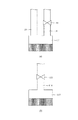
図1は一実施形態による蒸着装置を示す摸式断面図である。この装置は、例えば有機EL素子(有機発光素子)の製造に用いられる。真空チャンバー1の成膜空間において、被成膜基板である基板2上の素子分離膜3にマスク4を当接し、蒸着源5から蒸発又は昇華した蒸着材料である有機化合物をマスク4を介して基板2上に被着させ、有機化合物膜を成膜する。
FIG. 1 is a schematic sectional view showing a vapor deposition apparatus according to an embodiment. This apparatus is used, for example, for manufacturing an organic EL element (organic light emitting element). In the film formation space of the vacuum chamber 1, the mask 4 is brought into contact with the
蒸着源5には、蒸着材料6を充填した材料収容部7と、配管8,9を加熱するための手段である不図示のヒーターが備えられている。基板2の所定位置にだけ有機化合物を蒸着させるためのマスク4は、基板2の蒸着源側で、基板2に当接又は近接するように配設される。図1では、マスク4を基板2上に設けられた素子分離膜3の上面とほぼ接触するように配置している。また、基板2の裏面に配置した不図示の基板保持機構により、基板2及びマスク4が保持される。真空チャンバー1内は排気系により1×10⁻⁴〜1×10⁻⁵Pa程度に排気されている。
The
蒸着源5は、蒸着材料6を充填する材料収容部7が真空チャンバー1の外に設置され、1個の材料収容部7から複数本の配管8,9が真空チャンバー1内に繋がり、配管8、9を通って蒸着材料が基板2に到達する。
これらの配管は、図1に示すように、相対的にコンダクタンスが大きい配管8と小さい配管9を備える。また、3つ以上の異なるコンダクタンスを持つ配管を備えてもよい(図3参照)。
As shown in FIG. 1, these pipes include a pipe 8 having a relatively large conductance and a
ただし、どのような配管の組み合わせにおいても、コンダクタンスの小さい配管に、蒸着材料の流れを流量制御する、もしくは流れを開放・遮断する手段である流量調整機構10を備える。
However, in any combination of pipes, a pipe having a small conductance is provided with a flow
コンダクタンスの異なる配管は、コンダクタンス毎にそれぞれ何本備えていてもよい。そのうちの、コンダクタンスの小さい配管に、例えばバルブのような蒸着材料の流量制御、もしくは流れの開放・遮断を行う流量調整機構10を備える。流量調整機構10は、コンダクタンスが相対的に大きい配管に対して設定してもよいが、全ての配管に対して備えるか、又は1本以上の相対的にコンダクタンスが小さい配管に配置する。
Any number of pipes having different conductances may be provided for each conductance. Among them, a pipe having a small conductance is provided with a flow
本実施形態によれば、コンダクタンスの大きい配管8を備えることにより、蒸着材料の流量を高く保つことが可能になる。蒸着材料の流量は、加熱温度によって蒸着材料の流れを制御してもよく、バルブのような蒸着材料の流量を制御する手段を用いてもよい。 According to this embodiment, it is possible to keep the flow rate of the vapor deposition material high by providing the pipe 8 having a large conductance. As for the flow rate of the vapor deposition material, the flow of the vapor deposition material may be controlled by the heating temperature, or a means for controlling the flow rate of the vapor deposition material such as a valve may be used.
配管を流れる蒸着材料の流量の制御性は、加熱温度の制御性あるいはバルブの制御性によって制限されるが、複数本の配管と、配管内の流れの流量制御又は流れを開放・遮断するバルブ等を備えることにより、蒸着材料の流量を細かく制御することが可能になる。特に、コンダクタンスの小さい配管9を設置し、この配管9に対してバルブのよう流量調整機構10を備えることにより、この効果は大きくなる。このように、複数本の配管からの成膜速度の合成によって、高い成膜速度を安定に制御することが可能になる。
The controllability of the flow rate of the vapor deposition material flowing through the pipe is limited by the controllability of the heating temperature or the controllability of the valve, but there are multiple pipes and the flow rate control of the flow in the pipe or a valve that opens / closes the flow By providing the above, it becomes possible to finely control the flow rate of the vapor deposition material. In particular, by installing a
すなわち、コンダクタンスの大きい配管8によって高い成膜速度を保ち、コンダクタンスが小さくて、蒸着材料の流量を制御する、もしくは流れを開放・遮断する流量調整機構10を備えた配管9によって、微細な成膜速度の制御を行うことが可能となる。
That is, a high film formation rate is maintained by the pipe 8 having a large conductance, and a fine film is formed by the
材料収容部7は、真空チャンバー1の外に配置することが望ましい。蒸着材料が切れた場合に、真空を破らずに蒸着材料の再充填が可能となる。 It is desirable that the material container 7 be disposed outside the vacuum chamber 1. When the vapor deposition material is cut, the vapor deposition material can be refilled without breaking the vacuum.
次に、複数本の配管と、蒸着材料の流量を制御する流量調整機構を持つことによる効果を説明する。図2の(a)は、長さ、径が等しい2本の配管18を持つ材料収容部17を示す。2本の配管18のうちの1本は、蒸着材料の流量を制御する流量調整機構20としてバルブを備えている。
Next, the effect of having a plurality of pipes and a flow rate adjusting mechanism for controlling the flow rate of the vapor deposition material will be described. FIG. 2A shows a
バルブの流量の制御精度は3%とし、配管1本当たりのある温度における最大流量を50l/sとし、また、2本の配管18からの流量の目標を70l/sとする。
The control accuracy of the flow rate of the valve is 3%, the maximum flow rate at a certain temperature per pipe is 50 l / s, and the target of the flow rate from the two
バルブを持たない配管18は50l/sの流量を流し、バルブを持つ配管18は20l/sの流量をバルブによって制御する。材料の温度などの系の状態が理想的に一定に保たれるならば、この蒸着源は70±0.6l/sで流量を制御することができる。
The
図2の(b)は、流量調整機構120として上記と同様に3%の制御精度のバルブを持ち、最大流量が100l/sである配管118を1本だけ備えた材料収容部117を示す。流量の目標を70l/sとすると、この蒸着源は70±2.1l/sで流量を制御する。
FIG. 2B shows a
以上から、複数本の配管と、少なくとも1本の配管に流量調整機構を備えることにより、流量の微細な制御が可能になることがわかる。 From the above, it can be seen that the flow rate can be finely controlled by providing a plurality of pipes and at least one pipe with a flow rate adjusting mechanism.
図3の(a)に示すように、全ての配管28が同じ径、長さの場合は、成膜速度を好適に制御できるように、適当な数の配管28に対して、例えばバルブのような蒸着材料の流れを流量制御する、もしくは流れの開放・遮断を行う流量調整機構30を備える。この場合も、全ての配管に対して流量調整機構30を備えてもよい。
As shown in FIG. 3 (a), when all the
なお、蒸着源の構造、蒸着源の数、有機化合物の種類、マスクの開口形状などを特に制限するものではない。例えば蒸着源の開口形状は、点状であっても、線状であってもよい。 The structure of the vapor deposition source, the number of vapor deposition sources, the type of organic compound, the opening shape of the mask, etc. are not particularly limited. For example, the opening shape of the vapor deposition source may be a dot shape or a linear shape.
また、図4に示すように、図1の装置の配管8,9を連結する連結空間(連結部)11を設け、連結空間11に、真空チャンバー1の成膜空間に蒸着材料を放出するための放出部12を備えてもよい。
As shown in FIG. 4, a connecting space (connecting portion) 11 for connecting the
蒸着源は、複数の有機化合物を同時に蒸着する共蒸着源であってもよい。 The evaporation source may be a co-evaporation source that simultaneously deposits a plurality of organic compounds.
(参考例1)
図1に示す蒸着装置を用いて以下の蒸着方法によって基板上に有機EL素子を製造した。蒸着源5の材料収容部7は、コンダクタンスの大きい配管8を1本と、コンダクタンスの小さい配管9を2本備える。
(Reference Example 1)
An organic EL element was produced on a substrate by the following vapor deposition method using the vapor deposition apparatus shown in FIG. The material container 7 of the
目標成膜速度は20[Å/s]とした。コンダクタンスの大きい配管8は、この配管の直上の成膜速度を19[Å/s]前後に保つ。配管8における蒸着材料の流量は材料収容部7の加熱温度のみによって制御されるが、加熱温度は略一定とした。コンダクタンスの小さい配管9は、目標成膜速度をコンダクタンスの大きい配管8の直上において1[Å/s]となるようにした。配管9は、蒸着材料の流量を制御する流量調整機構10としてニードルバルブを設置した。
The target film formation rate was 20 [Å / s]. The pipe 8 having a large conductance keeps the film forming speed immediately above this pipe at around 19 [Å / s]. Although the flow rate of the vapor deposition material in the pipe 8 is controlled only by the heating temperature of the material container 7, the heating temperature is substantially constant. The
基板2には、無アルカリガラスの0.5mm厚でサイズが400mm×500mmのガラス基板を用いた。この基板2上に定法によって薄膜トランジスタ(TFT)と電極配線がマトリクス状に形成されている。一つの画素の大きさは30μm×120μmとし、有機EL素子の表示領域が350mm×450mmとなるように基板中央に配置した。基板2は蒸着源5から200[mm]の距離に置いた。また、基板2は略一定の速度で搬送しながら真空蒸着した。成膜速度は不図示の膜厚レートセンサーで観測し、ニードルバルブへフィードバックして制御を行った。
As the substrate 2, a non-alkali glass glass substrate having a thickness of 0.5 mm and a size of 400 mm × 500 mm was used. Thin film transistors (TFTs) and electrode wirings are formed in a matrix on the substrate 2 by a conventional method. One pixel had a size of 30 μm × 120 μm, and was arranged in the center of the substrate so that the display area of the organic EL element was 350 mm × 450 mm. The substrate 2 was placed at a distance of 200 [mm] from the
有機EL素子の作製工程を説明する。まず、発光領域が画素の中心部に25μm×100μmになるように、TFTを備えたガラス基板上にアノード電極を形成した。次に、本実施例の蒸着装置及び公知の蒸着マスク、発光材料を用いて真空蒸着することで、発光材料の成膜速度を20[Å/s]±2%で制御することが可能になった。以上により、基板上の画素内及び基板面内において発光層の膜厚を精度よく制御することが可能になり、高品位な有機EL素子が得られた。 A manufacturing process of the organic EL element will be described. First, an anode electrode was formed on a glass substrate provided with TFTs so that the light emitting region was 25 μm × 100 μm at the center of the pixel. Next, the deposition rate of the light emitting material can be controlled at 20 [Å / s] ± 2% by vacuum deposition using the vapor deposition apparatus of this embodiment, a known vapor deposition mask, and the light emitting material. It was. As described above, the film thickness of the light emitting layer can be accurately controlled in the pixels on the substrate and in the substrate surface, and a high-quality organic EL element can be obtained.
(参考例2)
図3の(a)に示す蒸着源を用いて基板上に有機EL素子を製造した。蒸着源は、材料収容部27にコンダクタンスを等しくした配管28を6本備えた。これらは材料収容部27の上面の中心から等距離、等間隔に配置した。6本の配管28のうちの2本に対して、蒸着材料の流量を制御する流量調整機構30としてニードルバルブを設置した。
(Reference Example 2)
An organic EL element was produced on the substrate using the vapor deposition source shown in FIG. The vapor deposition source was provided with six
目標成膜速度は20[Å/s]とした。ニードルバルブを持たない配管は、目標成膜速度を、材料収容部27の上面の中心の直上において1本当り4.5[Å/s]とした。この配管の蒸着材料の流量は材料収容部の加熱温度のみによって制御されるが、加熱温度は略一定とした。
The target film formation rate was 20 [Å / s]. The pipe without the needle valve has a target film forming speed of 4.5 [Å / s] per line just above the center of the upper surface of the
ニードルバルブを持つ配管は、目標成膜速度を、材料収容部27の中心の直上において1本当り1.0[Å/s]とした。
A pipe having a needle valve has a target film forming speed of 1.0 [Å / s] per line immediately above the center of the
蒸着源以外の構成は、参考例1と同様のものを用いた。 The configuration other than the vapor deposition source was the same as in Reference Example 1.
本参考例の蒸着装置及び公知の蒸着マスク、発光材料を用いて真空蒸着することで、発光材料の成膜速度を20[Å/s]±2%で制御することが可能になった。以上により、基板上の画素内及び基板面内において発光層の膜厚を精度よく制御することが可能になり、高品位な有機EL素子が得られた。 By performing vacuum deposition using the vapor deposition apparatus of this reference example, a known vapor deposition mask, and a light emitting material, the film forming speed of the light emitting material can be controlled at 20 [Å / s] ± 2%. As described above, the film thickness of the light emitting layer can be accurately controlled in the pixels on the substrate and in the substrate surface, and a high-quality organic EL element is obtained.
図3の(b)に示す蒸着源を用いて基板上に有機EL素子を製造した。蒸着源は、材料収容部37にコンダクタンスの大きい配管38を1本と、コンダクタンスを中程度に設定した配管39aを1本と、コンダクタンスの小さい配管39bを1本備えた。
An organic EL element was produced on the substrate using the vapor deposition source shown in FIG. The vapor deposition source was provided with one
目標成膜速度は20[Å/s]とした。コンダクタンスの大きい配管38は、この配管38の直上の成膜速度を15[Å/s]前後に保つ。この配管38の蒸着材料の流量は材料収容部37の加熱温度のみによって制御されるが、加熱温度は略一定とした。
The target film formation rate was 20 [Å / s]. The
コンダクタンスを中程度に設定した配管39aは、目標成膜速度をコンダクタンスの大きい配管38の直上において4.5[Å/s]となるようにした。配管39aは、蒸着材料の流量を制御する流量調整機構40としてニードルバルブを備える。
The
コンダクタンスの小さい配管39bは、目標成膜速度をコンダクタンスの大きい配管38の直上において0.5[Å/s]となるようにした。配管39bは、蒸着材料の流量を制御する流量調整機構40としてニードルバルブを備える。
The pipe 39b having a small conductance is set so that the target film formation rate is 0.5 [Å / s] immediately above the
蒸着源以外の構成は、参考例1と同様のものを用いた。 The configuration other than the vapor deposition source was the same as in Reference Example 1.
本実施例の蒸着装置及び公知の蒸着マスク、発光材料を用いて真空蒸着することで、発光材料の成膜速度を20[Å/s]±2%で制御することが可能になった。以上により、基板上の画素内及び基板面内において発光層の膜厚を精度よく制御することが可能になり、高品位な有機EL素子が得られた。 By performing vacuum deposition using the vapor deposition apparatus of the present embodiment, a known vapor deposition mask, and a light emitting material, the film forming speed of the light emitting material can be controlled at 20 [Å / s] ± 2%. As described above, the film thickness of the light emitting layer can be accurately controlled in the pixels on the substrate and in the substrate surface, and a high-quality organic EL element can be obtained.
図3の(b)に示す蒸着源を用いて基板上に有機EL素子を製造した。蒸着源は、材料収容部37にコンダクタンスの大きい配管38を1本と、コンダクタンスを中程度に設定した配管39aを1本と、コンダクタンスの小さい配管39bを1本備える。
An organic EL element was produced on the substrate using the vapor deposition source shown in FIG. The vapor deposition source includes one
目標成膜速度は20[Å/s]とした。コンダクタンスの大きい配管38は、この配管38の直上の成膜速度を15[Å/s]前後に保つ。配管38の蒸着材料の流量は材料収容部37の加熱温度のみによって制御されるが、加熱温度は略一定とした。
The target film formation rate was 20 [Å / s]. The
コンダクタンスを中程度に設定した配管39aは、目標成膜速度をコンダクタンスの大きい配管38の直上において5[Å/s]となるようにした。配管39aは、流れの開放・遮断を行う流量調整機構40としてニードルバルブを備える。
The
コンダクタンスの小さい配管39bは、目標成膜速度をコンダクタンスの大きい配管38の直上において0.2[Å/s]となるようにした。配管39bは、流れの開放・遮断を行う流量調整機構40としてニードルバルブを備える。
The pipe 39b having a small conductance is set so that the target film formation rate is 0.2 [Å / s] immediately above the
蒸着源以外の構成は、参考例1と同様のものを用いた。 The configuration other than the vapor deposition source was the same as in Reference Example 1.
本実施例の蒸着装置及び公知の蒸着マスク、発光材料を用いて真空蒸着した。このとき、成膜速度が20.3[Å/s]になった場合にニードルバルブを遮断し、19.7[Å/s]となった場合にニードルバルブの開放を行った。この結果、成膜速度を20[Å/s]±2%で制御することが可能になった。以上により、基板上の画素内及び基板面内において発光層の膜厚を精度よく制御することが可能になり、高品位な有機EL素子が得られた。 Vacuum deposition was performed using the deposition apparatus of this example, a known deposition mask, and a light emitting material. At this time, the needle valve was shut off when the deposition rate reached 20.3 [Å / s], and the needle valve was opened when 19.7 [Å / s]. As a result, the deposition rate can be controlled at 20 [Å / s] ± 2%. As described above, the film thickness of the light emitting layer can be accurately controlled in the pixels on the substrate and in the substrate surface, and a high-quality organic EL element can be obtained.
(比較例1)
図2の(b)に示す蒸着源を用いて基板上に有機EL素子を製造した。蒸着源は、材料収容部117に配管118を1本のみ備えた。この配管118は、蒸着材料の流量を制御する流量調整機構120としてニードルバルブを設置した。目標成膜速度は20[Å/s]とした。蒸着源以外の構成は、参考例1と同様のものを用いた。
(Comparative Example 1)
An organic EL element was manufactured on the substrate using the vapor deposition source shown in FIG. The vapor deposition source was provided with only one
本比較例の蒸着装置及び公知の蒸着マスク、発光材料を用いて真空蒸着したところ、発光材料の成膜速度は20[Å/s]±5%でバラツキが生じた。蒸着後、蒸着した発光層の膜厚を計測するとガラス基板面内に膜厚ムラがあり、得られた有機EL素子に表示ムラが生じた。 When vacuum deposition was performed using the vapor deposition apparatus of this comparative example, a known vapor deposition mask, and a light emitting material, the film formation rate of the light emitting material varied at 20 [Å / s] ± 5%. When the film thickness of the deposited light emitting layer was measured after vapor deposition, there was film thickness unevenness in the glass substrate surface, and display unevenness occurred in the obtained organic EL element.
1 真空チャンバー
2 基板
3 素子分離膜
4 マスク
5 蒸着源
6 蒸着材料
7 材料収容部
8、9、18、28、38、39a、39b 配管
10、20、30、40 流量調整機構
11 連結空間
12 放出部
DESCRIPTION OF SYMBOLS 1 Vacuum chamber 2
Claims (4)
成膜を行う成膜空間を有する真空チャンバーと、
前記蒸着材料を充填する材料収容部と、
前記材料収容部を加熱して前記蒸着材料を蒸発又は昇華させる手段と、
1個の前記材料収容部から前記真空チャンバーの前記成膜空間に配置された前記被成膜基板に向けて前記蒸着材料を供給するためのコンダクタンスの異なる複数本の配管と、を備え、
前記複数本の配管のうち、コンダクタンスの最も大きい配管に対して相対的にコンダクタンスの小さい配管に、前記蒸着材料の流れを流量制御又は開放・遮断する手段を設けることを特徴とする蒸着装置。 In a vapor deposition apparatus for depositing a vapor deposition material that has been evaporated or sublimated on a deposition target substrate,
A vacuum chamber having a film formation space for film formation;
A material container for filling the vapor deposition material;
Means for evaporating or sublimating the vapor deposition material by heating the material container;
A plurality of pipes having different conductances for supplying the vapor deposition material from one material accommodating portion toward the film formation substrate disposed in the film formation space of the vacuum chamber,
A vapor deposition apparatus characterized in that, among the plurality of pipes, a pipe having a relatively small conductance with respect to a pipe having the largest conductance is provided with means for controlling the flow rate of the vapor deposition material or opening / closing the flow of the vapor deposition material.
前記連結部から前記蒸着材料を前記真空チャンバーの前記成膜空間に放出する放出部と、を備えることを特徴とする請求項1に記載の蒸着装置。 A connecting portion for connecting the plurality of pipes;
Vapor deposition apparatus according to claim 1, characterized in that and a release unit for releasing the vapor deposition material in the deposition space of the vacuum chamber from said connecting portion.
Priority Applications (4)
| Application Number | Priority Date | Filing Date | Title |
|---|---|---|---|
| JP2007227408A JP5127372B2 (en) | 2007-09-03 | 2007-09-03 | Vapor deposition equipment |
| US12/193,612 US20090061084A1 (en) | 2007-09-03 | 2008-08-18 | Vapor deposition system and vapor deposition method |
| KR1020080086172A KR101037121B1 (en) | 2007-09-03 | 2008-09-02 | Vapor deposition system and vapor deposition method |
| CN2008102148949A CN101381859B (en) | 2007-09-03 | 2008-09-03 | Vapor deposition system and vapor deposition method |
Applications Claiming Priority (1)
| Application Number | Priority Date | Filing Date | Title |
|---|---|---|---|
| JP2007227408A JP5127372B2 (en) | 2007-09-03 | 2007-09-03 | Vapor deposition equipment |
Publications (3)
| Publication Number | Publication Date |
|---|---|
| JP2009057614A JP2009057614A (en) | 2009-03-19 |
| JP2009057614A5 JP2009057614A5 (en) | 2010-10-21 |
| JP5127372B2 true JP5127372B2 (en) | 2013-01-23 |
Family
ID=40407929
Family Applications (1)
| Application Number | Title | Priority Date | Filing Date |
|---|---|---|---|
| JP2007227408A Expired - Fee Related JP5127372B2 (en) | 2007-09-03 | 2007-09-03 | Vapor deposition equipment |
Country Status (4)
| Country | Link |
|---|---|
| US (1) | US20090061084A1 (en) |
| JP (1) | JP5127372B2 (en) |
| KR (1) | KR101037121B1 (en) |
| CN (1) | CN101381859B (en) |
Families Citing this family (2)
| Publication number | Priority date | Publication date | Assignee | Title |
|---|---|---|---|---|
| JP5367195B2 (en) * | 2011-03-15 | 2013-12-11 | シャープ株式会社 | Vapor deposition apparatus, vapor deposition method, and organic EL display device manufacturing method |
| DE102014014970B4 (en) | 2014-10-14 | 2020-01-02 | NICE Solar Energy GmbH | Device and method for measuring the layer thickness for vapor deposition processes |
Family Cites Families (9)
| Publication number | Priority date | Publication date | Assignee | Title |
|---|---|---|---|---|
| JPH0290662U (en) * | 1988-12-27 | 1990-07-18 | ||
| US6749906B2 (en) * | 2002-04-25 | 2004-06-15 | Eastman Kodak Company | Thermal physical vapor deposition apparatus with detachable vapor source(s) and method |
| JP4366226B2 (en) * | 2004-03-30 | 2009-11-18 | 東北パイオニア株式会社 | Organic EL panel manufacturing method, organic EL panel film forming apparatus |
| JP4476019B2 (en) * | 2004-05-20 | 2010-06-09 | 東北パイオニア株式会社 | Deposition source, vacuum film formation apparatus, organic EL element manufacturing method |
| JP2006057173A (en) * | 2004-08-24 | 2006-03-02 | Tohoku Pioneer Corp | Film deposition source, vacuum film deposition apparatus and method for producing organic el panel |
| JP4560394B2 (en) * | 2004-12-13 | 2010-10-13 | 長州産業株式会社 | Molecule supply equipment for thin film formation |
| JP4545028B2 (en) * | 2005-03-30 | 2010-09-15 | 日立造船株式会社 | Vapor deposition equipment |
| JP5064810B2 (en) * | 2006-01-27 | 2012-10-31 | キヤノン株式会社 | Vapor deposition apparatus and vapor deposition method |
| JP4966028B2 (en) * | 2007-01-15 | 2012-07-04 | パナソニック株式会社 | Vacuum deposition equipment |
-
2007
- 2007-09-03 JP JP2007227408A patent/JP5127372B2/en not_active Expired - Fee Related
-
2008
- 2008-08-18 US US12/193,612 patent/US20090061084A1/en not_active Abandoned
- 2008-09-02 KR KR1020080086172A patent/KR101037121B1/en active IP Right Grant
- 2008-09-03 CN CN2008102148949A patent/CN101381859B/en not_active Expired - Fee Related
Also Published As
| Publication number | Publication date |
|---|---|
| KR20090024081A (en) | 2009-03-06 |
| CN101381859A (en) | 2009-03-11 |
| CN101381859B (en) | 2011-03-02 |
| JP2009057614A (en) | 2009-03-19 |
| KR101037121B1 (en) | 2011-05-26 |
| US20090061084A1 (en) | 2009-03-05 |
Similar Documents
| Publication | Publication Date | Title |
|---|---|---|
| JP4767000B2 (en) | Vacuum deposition equipment | |
| JP5506147B2 (en) | Film forming apparatus and film forming method | |
| JP2009228091A (en) | Vapor deposition apparatus | |
| US20100097416A1 (en) | Organic dry jet printing head, and printing device and method using the same | |
| JP4545010B2 (en) | Vapor deposition equipment | |
| JP2008231573A (en) | Evaporation crucible and evaporation apparatus with adapted evaporation characteristic | |
| JP5244635B2 (en) | Organic vapor deposition equipment | |
| JP5127372B2 (en) | Vapor deposition equipment | |
| JP5328134B2 (en) | Vapor deposition apparatus and organic electroluminescence element manufacturing method | |
| CN107078215B (en) | Material source configuration and material distribution configuration for vacuum deposition | |
| JP2009057614A5 (en) | ||
| CN102301032A (en) | Vacuum Deposition Sources Having Heated Effusion Orifices | |
| KR20060013735A (en) | Crucible switching apparatus for continuous deposiotion in oled process | |
| JP5311985B2 (en) | Vapor deposition apparatus and organic light emitting device manufacturing method | |
| JP4445497B2 (en) | Thin film deposition apparatus and thin film deposition method using the same | |
| KR100624767B1 (en) | OLED evaporation system using shutter rotation for continuous deposition process | |
| KR20190090414A (en) | Deposition apparatus | |
| JP5460773B2 (en) | Film forming apparatus and film forming method | |
| JP2004010989A (en) | Thin-film forming apparatus | |
| KR102616040B1 (en) | Thin film deposition apparatus for forming patterned organic thin film and method of fabricating display device using the same | |
| KR102616039B1 (en) | Thin film deposition apparatus for forming patterned organic thin film | |
| KR100647578B1 (en) | Apparatus and Method for evaporation | |
| JP2009079244A (en) | Film deposition apparatus and film deposition method | |
| US11313033B2 (en) | Linear source apparatus, system and method of use | |
| KR20180112209A (en) | Thin Film Deposition Apparatus Easy to Separate Crucible |
Legal Events
| Date | Code | Title | Description |
|---|---|---|---|
| RD03 | Notification of appointment of power of attorney |
Free format text: JAPANESE INTERMEDIATE CODE: A7423 Effective date: 20090527 |
|
| A521 | Request for written amendment filed |
Free format text: JAPANESE INTERMEDIATE CODE: A523 Effective date: 20100903 |
|
| A621 | Written request for application examination |
Free format text: JAPANESE INTERMEDIATE CODE: A621 Effective date: 20100903 |
|
| A977 | Report on retrieval |
Free format text: JAPANESE INTERMEDIATE CODE: A971007 Effective date: 20111209 |
|
| A131 | Notification of reasons for refusal |
Free format text: JAPANESE INTERMEDIATE CODE: A131 Effective date: 20111213 |
|
| RD03 | Notification of appointment of power of attorney |
Free format text: JAPANESE INTERMEDIATE CODE: A7423 Effective date: 20120203 |
|
| A521 | Request for written amendment filed |
Free format text: JAPANESE INTERMEDIATE CODE: A523 Effective date: 20120213 |
|
| A131 | Notification of reasons for refusal |
Free format text: JAPANESE INTERMEDIATE CODE: A131 Effective date: 20120424 |
|
| A521 | Request for written amendment filed |
Free format text: JAPANESE INTERMEDIATE CODE: A523 Effective date: 20120619 |
|
| TRDD | Decision of grant or rejection written | ||
| A01 | Written decision to grant a patent or to grant a registration (utility model) |
Free format text: JAPANESE INTERMEDIATE CODE: A01 Effective date: 20121002 |
|
| A01 | Written decision to grant a patent or to grant a registration (utility model) |
Free format text: JAPANESE INTERMEDIATE CODE: A01 |
|
| A61 | First payment of annual fees (during grant procedure) |
Free format text: JAPANESE INTERMEDIATE CODE: A61 Effective date: 20121030 |
|
| R151 | Written notification of patent or utility model registration |
Ref document number: 5127372 Country of ref document: JP Free format text: JAPANESE INTERMEDIATE CODE: R151 |
|
| FPAY | Renewal fee payment (event date is renewal date of database) |
Free format text: PAYMENT UNTIL: 20151109 Year of fee payment: 3 |
|
| LAPS | Cancellation because of no payment of annual fees |