JP5127244B2 - Display device and electronic apparatus including the display device - Google Patents
Display device and electronic apparatus including the display device Download PDFInfo
- Publication number
- JP5127244B2 JP5127244B2 JP2007015719A JP2007015719A JP5127244B2 JP 5127244 B2 JP5127244 B2 JP 5127244B2 JP 2007015719 A JP2007015719 A JP 2007015719A JP 2007015719 A JP2007015719 A JP 2007015719A JP 5127244 B2 JP5127244 B2 JP 5127244B2
- Authority
- JP
- Japan
- Prior art keywords
- potential
- circuit
- line
- wiring
- signal
- Prior art date
- Legal status (The legal status is an assumption and is not a legal conclusion. Google has not performed a legal analysis and makes no representation as to the accuracy of the status listed.)
- Expired - Fee Related
Links
Images


Landscapes
- Liquid Crystal (AREA)
- Liquid Crystal Display Device Control (AREA)
- Control Of El Displays (AREA)
- Testing Electric Properties And Detecting Electric Faults (AREA)
- Control Of Indicators Other Than Cathode Ray Tubes (AREA)
Description
本発明は表示装置に関する。特に、表示装置の検査を簡略化し信頼性を向上させ、出荷歩留まりを向上させる検査回路を具備する表示装置に関する。また、検査回路を具備する表示装置に関し、検査回路によって検出された欠陥のあった表示装置に入力される信号を補正するための補正回路に関する。 The present invention relates to a display device. In particular, the present invention relates to a display device including an inspection circuit that simplifies inspection of a display device, improves reliability, and improves shipping yield. The present invention also relates to a display device including an inspection circuit, and to a correction circuit for correcting a signal input to a display device having a defect detected by the inspection circuit.
近年、TV、PCモニタ、モバイル用端末等を主な用途として、薄型ディスプレイの需要が急速に広がり、更なる開発が進められている。薄型ディスプレイとしては、液晶素子を用いた表示装置(Liquid Crystal Display;LCD)や発光素子を具備した表示装置がある。 In recent years, the demand for thin displays has rapidly expanded mainly for TVs, PC monitors, mobile terminals, and the like, and further development is being promoted. Examples of the thin display include a display device using a liquid crystal element (Liquid Crystal Display; LCD) and a display device including a light emitting element.
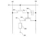
発光素子、液晶素子を用いた表示装置として、図20に示したアクティブマトリクス型の表示装置が挙げられる。 As a display device using a light-emitting element and a liquid crystal element, an active matrix display device shown in FIG. 20 can be given.
図20に示す表示装置は、基板2000上に、ゲート信号線駆動回路2001、ソース信号線駆動回路2002、画素部2003、及び複数の接続端子2004が形成された接続端子部2005を有する。ゲート信号線駆動回路2001にはゲートライン2006、ソース信号線駆動回路2002にはソースライン2007が接続されている。画素部2003における画素2008は、ゲートライン2006、ソースライン2007、電源線2009に接続されている。そして、画素2008には、ソースライン2007からの信号をゲートライン2006の信号により画素に設けられた発光素子または液晶素子に信号を書き込むためのトランジスタが設けられており、それぞれの画素においてトランジスタの各端子はゲートライン2006、ソースライン2007に接続されている。また、接続端子部2005には、外部からの信号を入力するためのFPC(Frexible Printed Circuit:フレキシブルプリントサーキット、図示せず)が接続される。そして基板2000は、画素2008に設けられた発光素子または液晶素子を封止するための対向基板2010を貼り付けることにより、表示モジュールとして完成する。
The display device illustrated in FIG. 20 includes a
図20において、画素部で表示を行う際、仮にゲートライン2006のLow電位をグランドとした場合、ソースライン2007のLow電位はゲートライン2006のLow電位より高い電位であり、且つ、ソースライン2007のLow電位とゲートライン2006のLow電位との差は、ゲートライン2006に接続された書き込みを行うためのトランジスタの閾値の電圧(Vth)分の値以上の電位であることが望ましい。ソースライン2007のLow電位がゲートライン2006のLow電位より低く、且つ、ソースライン2007のLow電位とゲートライン2006のLow電位との差が、書き込みを行うためのトランジスタの閾値の電圧(Vth)分の値未満の場合、書き込みを行うためのトランジスタから電流がリークしやすくなってしまい、表示装置は正常な表示を行うことができない。
In FIG. 20, when display is performed in the pixel portion, if the low potential of the
なお、ソースライン及びゲートラインのHigh電位とLow電位とは、それぞれ相対的に電位が高い場合と低い場合とを示しており、High電位は、トランジスタがオンとなるような値、Low電位は、トランジスタがオフとなるような値となるようにHigh電位とLow電位とで所定の電位差を有するように決定すればよい。 Note that the high potential and the low potential of the source line and the gate line respectively indicate a case where the potential is relatively high and a case where the potential is low. The high potential is a value at which the transistor is turned on and the low potential is What is necessary is just to determine so that it may have a predetermined potential difference with a High electric potential and a Low electric potential so that it may become a value which turns off a transistor.
図20における液晶素子や発光素子を用いた表示装置では、ゲート信号線駆動回路及びソース信号線駆動回路からの信号の電位関係によって画素を駆動させている。そのため、製造工程及び商品出荷工程では、ゲート信号線駆動回路及びソース信号線駆動回路からの信号の電位を検査することにより、上述の電位が保持されなくなるといった表示装置の不良検出が可能であることが望ましい。 In the display device using the liquid crystal element or the light-emitting element in FIG. 20, the pixel is driven by the potential relationship of signals from the gate signal line driver circuit and the source signal line driver circuit. Therefore, in the manufacturing process and the product shipping process, it is possible to detect a defect in the display device such that the above-described potential is not held by inspecting the potential of the signal from the gate signal line driver circuit and the source signal line driver circuit. Is desirable.
そのため、発光素子または液晶素子を用いた表示装置において、表示装置の不良の検査を行うためには、図21(A)のように一度完成したモジュールのうち、サンプルとして図21(B)のように対向基板をはがして測定機器によるプローブ2101を用いて検査を行う、または対向基板と貼り合わせる前に、測定機器によるプローブを用いて検査を行っていた(例えば特許文献1を参照)。
従来の液晶素子や発光素子を用いた表示装置においては、ゲート信号線駆動回路及びソース信号線駆動回路から画素までは表示装置の封止領域内に位置している。そのため、製造工程後に全ての表示モジュールの対向基板をはがして検査を行うことや対向基板の貼り合わせ工程以降での電位関係の検査は極めて難しく、対向基板の貼り合わせ工程〜出荷間での不良発見が十分行われていなかった。 In a conventional display device using a liquid crystal element or a light emitting element, the gate signal line driver circuit and the source signal line driver circuit to the pixels are located in the sealing region of the display device. For this reason, it is extremely difficult to perform inspection by peeling off the counter substrate of all display modules after the manufacturing process and inspecting the potential relationship after the counter substrate bonding process, and finding defects between the counter substrate bonding process and shipment. Was not done enough.
また、特許文献1に記載の方法では、製造工程以降で不良が発見された場合、不良のリペアができず出荷歩留まりを悪化する可能性や、外部部品での不良改善による製造コストの増加など悪影響が発生していた。 In addition, in the method described in Patent Document 1, if a defect is found after the manufacturing process, the defect cannot be repaired, and the shipping yield may be deteriorated. Had occurred.
また、単にソースライン、ゲートラインを配線で接続端子部まで引き延ばし、対向基板と貼り合わせた後の工程において、接続端子部の電位を測定することで検査を行うこともある。しかしながら、配線の引き回しに起因する寄生容量での電圧降下や遅延などの要素が含まれるため検査として不十分であった。 In some cases, the source line and the gate line are simply extended to the connection terminal portion by wiring and bonded to the counter substrate, and then the inspection is performed by measuring the potential of the connection terminal portion. However, it is not sufficient as an inspection because it includes elements such as a voltage drop and a delay in the parasitic capacitance caused by the wiring.
そこで本発明では、対向基板と貼り合わせた後の工程及び出荷前検査において、確度の高い検査回路を有する表示装置、また不良が発生した場合の表示装置内部における補正回路を具備する表示装置を提供することを課題とする。 Accordingly, the present invention provides a display device having a highly accurate inspection circuit in a process after bonding to a counter substrate and a pre-shipment inspection, and a display device including a correction circuit inside the display device when a defect occurs. The task is to do.
上述の諸問題を解決するため、本発明は画素部の不良を判別するための検査回路を設けることを特徴とする。そして、検査回路より出力される信号が配線を介して接続端子に出力されることを特徴とする。また、本発明は、当該検査回路より出力される信号により、画素部の不良を補正するための補正回路が設けられていることを特徴とする。以下、本発明の具体的な構成について示す。 In order to solve the above-described problems, the present invention is characterized in that an inspection circuit for determining a defect in the pixel portion is provided. A signal output from the inspection circuit is output to the connection terminal through the wiring. Further, the invention is characterized in that a correction circuit for correcting a defect of the pixel portion is provided by a signal output from the inspection circuit. Hereinafter, a specific configuration of the present invention will be described.
本発明の表示装置の一は、ゲートラインと、ソースラインと、ゲートライン及びソースラインの電位により駆動される画素部と、ゲートラインと平行に配置された第1の配線と、ソースラインと平行に配置された第2の配線と、第1の配線及び第2の配線に接続された検査回路と、を有し、検査回路は、第1の配線及び第2の配線の電位により、画素部の不良を判別する信号を出力することを特徴とする表示装置である。 One embodiment of the display device of the present invention includes a gate line, a source line, a pixel portion driven by the potential of the gate line and the source line, a first wiring arranged in parallel with the gate line, and a parallel to the source line. And a test circuit connected to the first wiring and the second wiring, and the test circuit uses the potential of the first wiring and the second wiring to generate a pixel portion. The display device is characterized in that it outputs a signal for discriminating defects.
また、別の本発明の表示装置の一は、ゲートラインと、ソースラインと、ゲートライン及びソースラインの電位により駆動される画素部と、ゲートラインと平行に配置された第1の配線と、ソースラインと平行に配置された第2の配線と、第1の配線及び第2の配線に接続された検査回路と、検査回路に接続された第1の接続端子及び第2の接続端子と、を有し、検査回路は、第1の配線及び第2の配線に接続された第1の回路と、第2の配線に接続された第2の回路と、第1の配線及び第2の回路に接続された第3の回路と、を有し、第1の回路は、第1の配線の電位と第2の配線の電位とを比較し、第2の配線の電位が第1の配線の電位を下回った場合に第1の電位を第1の接続端子に出力し、第2の回路は、第2の配線の電位から基準となる電位を減算した第2の電位を第3の回路に入力し、第3の回路は、第1の配線の電位と第2の電位とを比較し、第2の電位が第1の配線の電位を下回った場合に第3の電位を第2の接続端子に出力することを特徴とする表示装置である。 Another display device of the present invention includes a gate line, a source line, a pixel portion driven by the potential of the gate line and the source line, a first wiring arranged in parallel with the gate line, A second wiring arranged in parallel with the source line, a first wiring and a test circuit connected to the second wiring, a first connection terminal and a second connection terminal connected to the test circuit, The inspection circuit includes a first circuit connected to the first wiring and the second wiring, a second circuit connected to the second wiring, and the first wiring and the second circuit. And the first circuit compares the potential of the first wiring with the potential of the second wiring, and the potential of the second wiring is equal to that of the first wiring. When the potential falls below the first potential, the first potential is output to the first connection terminal, and the second circuit uses the second wiring as the reference Is input to the third circuit, and the third circuit compares the potential of the first wiring with the second potential, and the second potential is In the display device, the third potential is output to the second connection terminal when the potential is lower than the potential.
また別の本発明の表示装置の一は、ゲートラインと、ソースラインと、ゲートライン及びソースラインの電位により駆動される画素部と、ゲートラインと平行に配置された第1の配線と、ソースラインと平行に配置された第2の配線と、第1の配線及び第2の配線に接続された検査回路と、検査回路に接続された補正回路と、検査回路に接続された第1の接続端子及び第2の接続端子と、を有し、検査回路は、第1の配線及び第2の配線に接続された第1の回路と、第2の配線に接続された第2の回路と、第1の配線及び第2の回路に接続された第3の回路と、を有し、第1の回路は、第1の配線の電位と第2の配線の電位とを比較し、第2の配線の電位が第1の配線の電位を下回った場合に第1の電位を第1の接続端子に出力し、第2の回路は、第2の配線の電位から基準となる電位を減算した第2の電位を第3の回路に入力し、第3の回路は、第1の配線の電位と第2の電位とを比較し、第2の電位が第1の配線の電位を下回った場合に第3の電位を第2の接続端子に出力し、補正回路は、第2の接続端子に第3の電位が出力された際に、第2の配線の電位を第1の配線の電位よりも高くすることにより、第1の接続端子及び第2の接続端子に出力される電位の補正を行うことを特徴とする表示装置である。 Another display device of the present invention includes a gate line, a source line, a pixel portion driven by a potential of the gate line and the source line, a first wiring arranged in parallel with the gate line, and a source A second wiring arranged in parallel with the line, a test circuit connected to the first wiring and the second wiring, a correction circuit connected to the test circuit, and a first connection connected to the test circuit A test circuit, a first circuit connected to the first wiring and the second wiring, a second circuit connected to the second wiring, and a second circuit connected to the second wiring; And a third circuit connected to the first wiring and the second circuit, the first circuit compares the potential of the first wiring with the potential of the second wiring, and the second circuit When the potential of the wiring is lower than the potential of the first wiring, the first potential is output to the first connection terminal, and the second time Inputs a second potential obtained by subtracting a reference potential from the potential of the second wiring to the third circuit, and the third circuit compares the potential of the first wiring with the second potential. When the second potential is lower than the potential of the first wiring, the third potential is output to the second connection terminal, and the correction circuit outputs the third potential to the second connection terminal. In addition, in the display device, the potential output to the first connection terminal and the second connection terminal is corrected by making the potential of the second wiring higher than the potential of the first wiring. is there.
また別の本発明の表示装置の一は、ゲートラインと、ソースラインと、ソースラインに信号を供給する駆動回路と、ゲートライン及びソースラインの電位により駆動される画素部と、ゲートライン及びソースラインに接続された切り替え回路と、検査回路と、を有し、切り替え回路は、ソースラインの書き込みを制御する信号が駆動回路に供給されない場合に、ゲートライン及びソースラインと検査回路とを接続させ、検査回路は、入力されたゲートラインの電位及びソースラインの電位により画素部の不良を判別する信号を出力することを特徴とする表示装置である。 Another display device of the present invention includes a gate line, a source line, a driver circuit for supplying a signal to the source line, a pixel portion driven by a potential of the gate line and the source line, a gate line and a source A switching circuit connected to the line, and an inspection circuit. The switching circuit connects the gate line and the source line to the inspection circuit when a signal for controlling writing of the source line is not supplied to the driver circuit. The inspection circuit is a display device that outputs a signal for determining a defect of the pixel portion based on the inputted potential of the gate line and the potential of the source line.
また別の本発明の表示装置の一は、ゲートラインと、ソースラインと、ソースラインに信号を供給する駆動回路と、ゲートライン及びソースラインの電位により駆動される画素部と、ゲートライン及びソースラインに接続された切り替え回路と、検査回路と、検査回路に接続された第1の接続端子及び第2の接続端子と、を有し、検査回路は、ゲートライン及びソースラインに接続された第1の回路と、ソースラインに接続された第2の回路と、ゲートライン及び第2の回路に接続された第3の回路と、を有し、切り替え回路は、ソースラインの書き込みを制御する信号が駆動回路に供給されない場合に、ゲートライン及びソースラインと検査回路とを接続させ、第1の回路は、入力されたゲートラインの電位とソースラインより入力された電位とを比較し、入力されたソースラインの電位がゲートラインの電位を下回った場合に第1の電位を第1の接続端子に出力し、第2の回路は、入力されたソースラインの電位から基準となる電位を減算した第2の電位を第3の回路に入力し、第3の回路は、入力されたゲートラインの電位と第2の電位とを比較し、第2の電位がゲートラインの電位を下回った場合に第3の電位を第2の接続端子に出力することを特徴とする表示装置である。 Another display device of the present invention includes a gate line, a source line, a driver circuit for supplying a signal to the source line, a pixel portion driven by a potential of the gate line and the source line, a gate line and a source A switching circuit connected to the line; an inspection circuit; and a first connection terminal and a second connection terminal connected to the inspection circuit, wherein the inspection circuit is connected to the gate line and the source line. 1 circuit, a second circuit connected to the source line, and a third circuit connected to the gate line and the second circuit, and the switching circuit controls the writing of the source line Is not supplied to the driver circuit, the gate line and the source line are connected to the inspection circuit, and the first circuit is input from the potential of the input gate line and the source line. The first circuit outputs the first potential to the first connection terminal when the input source line potential is lower than the gate line potential, and the second circuit outputs the input source line potential. The second potential obtained by subtracting the reference potential is input to the third circuit, and the third circuit compares the input potential of the gate line with the second potential, and the second potential is the gate potential. In the display device, the third potential is output to the second connection terminal when the potential is lower than the potential of the line.
また別の本発明の表示装置の一は、ゲートラインと、ソースラインと、ソースラインに信号を供給する駆動回路と、ゲートライン及びソースラインの電位により駆動される画素部と、ゲートライン及びソースラインに接続された切り替え回路と、検査回路と、検査回路に接続された第1の接続端子及び第2の接続端子と、検査回路及び第2の接続端子に接続された補正回路と、を有し、検査回路は、ゲートライン及びソースラインに接続された第1の回路と、ソースラインに接続された第2の回路と、ゲートライン及び第2の回路に接続された第3の回路と、を有し、切り替え回路は、ソースラインに書き込みを制御する信号が駆動回路に供給されない場合に、ゲートライン及びソースラインと検査回路とを接続させ、第1の回路は、入力されたゲートラインの電位とソースラインの電位とを比較し、ソースラインの電位がゲートラインの電位を下回った場合に第1の電位を第1の接続端子に出力し、第2の回路は、入力されたソースラインの電位から基準となる電位を減算した第2の電位を第3の回路に入力し、第3の回路は、入力されたゲートラインの電位と第2の電位とを比較し、第2の電位がゲートラインの電位を下回った場合に第3の電位を第2の接続端子に出力し、補正回路は、第2の接続端子に第3の電位が出力された際に、ソースラインの電位をゲートラインの電位よりも高くすることにより、第1の接続端子及び第2の接続端子に出力される電位の補正を行うことを特徴とする表示装置である。 Another display device of the present invention includes a gate line, a source line, a driver circuit for supplying a signal to the source line, a pixel portion driven by a potential of the gate line and the source line, a gate line and a source A switching circuit connected to the line, an inspection circuit, a first connection terminal and a second connection terminal connected to the inspection circuit, and a correction circuit connected to the inspection circuit and the second connection terminal. The inspection circuit includes a first circuit connected to the gate line and the source line, a second circuit connected to the source line, a third circuit connected to the gate line and the second circuit, And the switching circuit connects the gate line and the source line to the inspection circuit when the signal for controlling writing to the source line is not supplied to the driver circuit, and the first circuit receives the input signal. The potential of the gate line and the potential of the source line are compared, and when the potential of the source line is lower than the potential of the gate line, the first potential is output to the first connection terminal. A second potential obtained by subtracting a reference potential from the source line potential is input to the third circuit, and the third circuit compares the input gate line potential with the second potential; When the second potential is lower than the potential of the gate line, the third potential is output to the second connection terminal, and the correction circuit generates a source when the third potential is output to the second connection terminal. The display device is characterized in that the potential output to the first connection terminal and the second connection terminal is corrected by making the potential of the line higher than the potential of the gate line.
また本発明において、第1接続端子及び第2の接続端子は、画素部が形成された基板と対向基板により封止される領域の外側に設けられていてもよい。 In the present invention, the first connection terminal and the second connection terminal may be provided outside a region sealed by the substrate on which the pixel portion is formed and the counter substrate.
また本発明において、画素部は、ゲートライン及びソースラインに接続されたトランジスタを有し、トランジスタは、ゲートラインに入力される信号により選択され、ソースラインからの信号が書き込まれる構成であってもよい。 In the present invention, the pixel portion includes a transistor connected to the gate line and the source line, and the transistor is selected by a signal input to the gate line and a signal from the source line is written. Good.
また本発明において、トランジスタは、Nチャネル型トランジスタであってもよい。 In the present invention, the transistor may be an N-channel transistor.
また、別の本発明の一は、本明細書に記載した表示装置を表示部に備えたことを特徴とする電子機器である。 Another aspect of the present invention is an electronic device including the display device described in this specification in a display portion.
なお、本発明の表示装置には、有機発光素子(OLED)に代表される発光素子を各画素に備えた表示装置の他、液晶表示装置、DMD(Digital Micromirror Device)、PDP(Plasma Display Panel)、FED(Field Emission Display)ゲートラインとソースラインに入力される信号により表示を行う表示装置がその範疇に含まれる。 Note that the display device of the present invention includes a liquid crystal display device, a DMD (Digital Micromirror Device), and a PDP (Plasma Display Panel) in addition to a display device including a light emitting element typified by an organic light emitting element (OLED) in each pixel. , A display device that performs display by signals input to a FED (Field Emission Display) gate line and a source line is included in its category.
また、本明細書において発光素子は、電流または電圧によって輝度が制御される素子をその範疇に含んでいる。具体的にはOLED(Organic Light Emitting Diode)や、無機EL(Electro luminescence)や、FED(Field Emission Display)に用いられているMIM型の電子源素子(電子放出素子)等が含まれる。 In this specification, a light-emitting element includes an element whose luminance is controlled by current or voltage in its category. Specifically, an OLED (Organic Light Emitting Diode), an inorganic EL (Electro Luminescence), a MIM type electron source element (electron emitting element) used in FED (Field Emission Display), and the like are included.
また、表示装置は、発光素子が封止された状態にあるパネルと、該パネルにコントローラを含むIC等を実装した状態にあるモジュールとを含む。また表示装置は、液晶素子が封止された状態にあるパネルと、該パネルにコントローラを含むIC等を実装した状態にあるモジュールとを含む。 The display device includes a panel in which the light-emitting element is sealed, and a module in which an IC including a controller is mounted on the panel. The display device includes a panel in which the liquid crystal element is sealed and a module in which an IC including a controller is mounted on the panel.
なお、本発明の表示装置において用いられるトランジスタとして、多結晶半導体、微結晶半導体(セミアモルファス半導体を含む)、アモルファス半導体を用いた薄膜トランジスタを用いることができるが、本発明の表示装置に用いられるトランジスタは薄膜トランジスタに限定されない。単結晶シリコンを用いて形成されたトランジスタであっても良いし、SOIを用いたトランジスタであっても良い。また、有機半導体を用いたトランジスタであっても良いし、カーボンナノチューブを用いたトランジスタであってもよいし、酸化亜鉛を用いたトランジスタであってもよい。また本発明の表示装置の画素に設けられたトランジスタは、シングルゲート構造を有していても良いし、ダブルゲート構造や3個以上のゲートを有するマルチゲート構造であっても良い。 Note that as a transistor used in the display device of the present invention, a polycrystalline semiconductor, a microcrystalline semiconductor (including a semi-amorphous semiconductor), or a thin film transistor using an amorphous semiconductor can be used; however, the transistor used in the display device of the present invention Is not limited to a thin film transistor. A transistor formed using single crystal silicon or a transistor using SOI may be used. In addition, a transistor using an organic semiconductor, a transistor using carbon nanotubes, or a transistor using zinc oxide may be used. Further, the transistor provided in the pixel of the display device of the present invention may have a single gate structure, a double gate structure, or a multi-gate structure having three or more gates.
本発明により、検査回路を具備する構成にすることにより、対向基板と貼り合わせる前の工程や貼り合わせた後に対向基板をはがすことでしか実施できなかった表示装置の検査が任意の工程において実施することができる。そのため、対向基板と貼り合わせた後の工程であっても、ゲートラインとソースラインの電位関係による表示装置の表示不良を検出することができる。 In accordance with the present invention, by adopting a configuration including an inspection circuit, inspection of a display device that can only be performed by peeling off the counter substrate after bonding or bonding to the counter substrate is performed in any step. be able to. Therefore, even in the process after bonding to the counter substrate, a display defect of the display device due to the potential relationship between the gate line and the source line can be detected.
また本発明は、検査回路を具備する構成に加えて、補正回路を具備する構成とする。よって本発明の表示装置は、検査回路より出力される不良を判別するための信号に基づいて、ゲートラインとソースラインの電位関係による表示装置の表示不良を表示装置単体で補正することが可能になる。そのため、表示装置の検査、補正を確実に行うことができ、出荷歩留まりを向上することができる。 Further, the present invention has a configuration including a correction circuit in addition to the configuration including the inspection circuit. Therefore, the display device of the present invention can correct the display defect of the display device due to the potential relationship between the gate line and the source line by the display device alone based on the signal for determining the defect output from the inspection circuit. Become. Therefore, the inspection and correction of the display device can be performed reliably, and the shipping yield can be improved.
以下に、本発明の実施の形態を図面に基づいて説明する。但し、本発明は多くの異なる態様で実施することが可能であり、本発明の趣旨及びその範囲から逸脱することなくその形態及び詳細を様々に変更し得ることは当業者であれば容易に理解される。従って、本実施の形態の記載内容に限定して解釈されるものではない。なお、実施の形態を説明するための全図において、同一部分又は同様な機能を有する部分には同一の符号を付し、その繰り返しの説明は省略する。
(実施の形態1)
Embodiments of the present invention will be described below with reference to the drawings. However, the present invention can be implemented in many different modes, and those skilled in the art can easily understand that the modes and details can be variously changed without departing from the spirit and scope of the present invention. Is done. Therefore, the present invention is not construed as being limited to the description of this embodiment mode. Note that in all the drawings for describing the embodiments, the same portions or portions having similar functions are denoted by the same reference numerals, and repetitive description thereof is omitted.
(Embodiment 1)
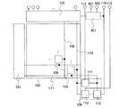
図1に本実施の形態における表示装置のブロック図について示し、以下詳細に説明する。なお、本発明において表示装置とは、表示素子(液晶素子や発光素子など)を有する装置のことを言う。なお、基板上に液晶素子やEL素子などの表示素子を含む複数の画素やそれらの画素を駆動させる周辺駆動回路が形成された表示パネル本体のことでもよい。さらに、フレキシブルプリントサーキット(FPC)やプリント配線基盤(PWB)が取り付けられたものも含んでもよい。また、発光装置とは、特にEL素子やFEDで用いる素子などの自発光型の表示素子を有している表示装置をいう。液晶表示装置とは、液晶素子を有している表示装置をいう。 FIG. 1 shows a block diagram of a display device in this embodiment mode, which will be described in detail below. Note that a display device in the present invention refers to a device having a display element (a liquid crystal element, a light-emitting element, or the like). Note that a display panel body in which a plurality of pixels including a display element such as a liquid crystal element or an EL element and a peripheral driver circuit for driving these pixels are formed over a substrate may be used. Furthermore, the display device may include one provided with a flexible printed circuit (FPC) or a printed wiring board (PWB). A light-emitting device refers to a display device including a self-luminous display element such as an EL element or an element used in an FED. A liquid crystal display device refers to a display device having a liquid crystal element.
図1に本発明の基本構成について示す。図1に示す表示装置は、基板100上に、ゲート信号線駆動回路101、ソース信号線駆動回路102、画素部103、及び複数の接続端子104が形成された接続端子部105、検査回路106を有する。ゲート信号線駆動回路101にはゲートライン107、ソース信号線駆動回路102にはソースライン108が接続されている。画素部103における画素109は、ゲートライン107及びソースライン108に接続されている。そして、画素109には、ソースライン108からの信号をゲートライン107の信号により画素に設けられた発光素子または液晶素子に書き込むためのトランジスタが設けられており、それぞれの画素においてトランジスタの各端子はゲートライン107、ソースライン108に接続されている。また、接続端子部105には、外部からの信号を入力するためのFPC(Flexible Printed Circuit:フレキシブルプリントサーキット、図示せず)が接続される。そして基板100は、画素109に設けられた発光素子または液晶素子を封止するための対向基板110を貼り付けることにより、表示モジュールとして完成する。
FIG. 1 shows the basic configuration of the present invention. The display device illustrated in FIG. 1 includes a gate signal
検査回路106は、ゲートラインと平行方向に形成されたダミーのゲートライン(第1の配線ともいう)117がゲート信号線駆動回路101と、ソースラインと平行方向に形成されたダミーのソースライン(第2の配線ともいう)118がソース信号線駆動回路102とそれぞれ接続された部分と画素部103を挟んで反対側に設けられ、ダミーのゲートライン117と、ダミーのソースライン118と接続されている。本実施の形態において、ダミーのゲートライン117は、ゲートラインの一つを表示装置において表示に寄与する画素とは異なる画素に接続させたダミーラインであり、ゲートライン107と同時に形成され、ゲートライン107と同様の信号が供給される。またダミーのソースライン118は、ソースライン108の一つを表示装置において表示に寄与する画素とは異なる画素に接続させたダミーラインであり、ソースライン108と同時に形成され、ソースライン108と同様の信号が供給される。また、本実施の形態において、他の画素と同ラインに設けられ表示に寄与しない画素をダミー画素という。前述のダミー画素、ダミーのゲートライン117及びダミーのソースライン118は、検査回路106に接続されることで表示に影響を与えないように設けられるものである。ダミー画素については表示面を遮光することで、他の画素表示に影響を与えることなく検査が可能にすることができる。なお、ゲートラインと同様の信号が供給されるとは、ゲートライン107と同時に形成される、つまり同じ材料で構成されるものであるとする。またソースラインと同様の信号が供給されるとは、ソースライン108と同時に形成される、つまり同じ材料で構成されるものであるとする。
The
また、検査回路106は、画素部におけるゲートライン107及びソースライン108の電位関係について、ソースライン108の電位がゲートライン107の電位より低く、且つ、ソースライン108のLow電位とゲートライン107のLow電位との差がソースライン108からの信号の書き込みをおこなうためのトランジスタの閾値の電圧(Vth)分の値未満になった場合に起因する不良を検出する。具体的に検査回路106には、ダミーのゲートライン117の電位と、ダミーのソースライン118の電位を比較し、ダミーのゲートライン117の電位をダミーのソースライン118の電位が下回ったときにHigh電位を出力する第1の回路111(第1の比較回路ともいう)と、ダミーのソースライン118の電位から基準となる電位を減算し、出力する第2の回路112(減算回路ともいう)と、ダミーのゲートライン117の電位を第2の回路112の出力と比較し、出力する第3の回路113(第2の比較回路ともいう)が設けられている。そして検査回路106は、引き回された配線により、第1の回路111で比較した結果を出力するための接続端子114、第2の回路112に基準となる電位が入力される接続端子115、第3の回路113からの信号を出力するための接続端子116がそれぞれ接続端子部105から検査回路106に接続される。なお第2の回路112に入力される基準となる電位とは、本明細書では、画素に設けられたソースラインからの信号の書き込みをおこなうためのトランジスタの閾値の電圧(Vth)とほぼ同じ電位が望ましく、0.1〜2.0V程度であることが望ましい。
In the
また、画素109の画素構成について図2、図3に具体的な例を挙げる。本実施の形態では表示媒体として、図2に発光素子、図3に液晶素子を用いた代表的な画素構成について説明する。
Specific examples of the pixel configuration of the
図2では表示媒体に発光素子を用い、ソースラインからの信号の書き込みをおこなう第1のトランジスタ201(書き込みトランジスタともいう)にNチャネル型トランジスタ、発光素子の駆動を行うための第2のトランジスタ202(駆動トランジスタともいう)にPチャネル型トランジスタを用いた場合の画素構成について示す。
In FIG. 2, a light-emitting element is used as a display medium, an N-channel transistor is used as a first transistor 201 (also referred to as a writing transistor) that performs signal writing from a source line, and a
図2において、ゲートライン107がHigh電位となるとき、第1のトランジスタ201がオンし、ソースライン108の電位が保持容量203に保持され、節点Ngの電位に反映される。またゲートライン107がLow電位となるときは、第1のトランジスタ201がオフし、ソースライン108の電位にかかわらず保持容量203に保持された電位が節点Ngの電位に反映される。節点Ndの電位は、節点Ngの電位がHigh電位のとき、第2のトランジスタ202がオフしているので、Low電位となる。また、節点Ndの電位は、節点Ngの電位がLow電位のとき、第2のトランジスタ202がオンしているので、電源線204から電流が流れ、High電位となる。この節点Ndの電位は、発光素子205を通り、対向電極206へと流れる。
In FIG. 2, when the
なお、本明細書中において、トランジスタがオンしているとは、トランジスタのゲートとソースの間の電圧がその閾値電圧を超え、ソースとドレインの間に電流が流れる状態を指し、トランジスタがオフしているとは、トランジスタのゲートとソースの間の電圧がその閾値電圧を下回り、ソースとドレインの間に電流が流れていない状態を指す。 Note that in this specification, a transistor is on refers to a state in which the voltage between the gate and the source of the transistor exceeds the threshold voltage and current flows between the source and the drain, and the transistor is turned off. In this case, the voltage between the gate and the source of the transistor is lower than the threshold voltage, and no current flows between the source and the drain.
また、本明細書において、一画素とは、明るさを制御できる要素一つ分を示すものとする。よって、一例としては、一画素とは、一つの色要素を示すものとし、その色要素一つで明るさを表現する。従って、そのときは、R(赤)G(緑)B(青)の色要素からなるカラー表示装置の場合には、画像の最小単位は、Rの画素とGの画素とBの画素との三画素から構成されるものとする。なお、色要素は、三色に限定されず、三色以上用いてもよく、例えば、RGBW(Wは白)がある。また、別の例としては、1つの色要素について、複数の領域を用いて明るさを制御する場合は、その領域一つ分を一画素とする。よって、一例としては、面積階調を行う場合、一つの色要素につき、明るさを制御する領域が複数あり、その全体で階調を表現するわけであるが、明るさを制御する領域の一つ分を一画素とする。よって、その場合は、一つの色要素は、複数の画素で構成されることとなる。また、その場合、画素によって、表示に寄与する領域の大きさが異なっている場合がある。また、一つの色要素につき複数ある、明るさを制御する領域において、つまり、一つの色要素を構成する複数の画素において、各々に供給する信号を僅かに異ならせるようにして、視野角を広げるようにしてもよい。なお、一画素(三色分)と記載する場合は、RとGとBの三画素分を一画素と考える場合であるとする。一画素(一色分)と記載する場合は、一つの色要素につき、複数の画素がある場合、それらをまとめて一画素と考える場合であるとする。 In this specification, one pixel means one element whose brightness can be controlled. Therefore, as an example, one pixel represents one color element, and brightness is expressed by one color element. Therefore, at that time, in the case of a color display device composed of R (red), G (green), and B (blue) color elements, the minimum unit of an image is an R pixel, a G pixel, and a B pixel. It is assumed to be composed of three pixels. The color elements are not limited to three colors, and three or more colors may be used, for example, RGBW (W is white). As another example, in the case where brightness is controlled using a plurality of areas for one color element, one area corresponds to one pixel. Therefore, as an example, when performing area gradation, there are a plurality of areas for controlling the brightness for each color element, and the gradation is expressed as a whole. One portion is defined as one pixel. Therefore, in that case, one color element is composed of a plurality of pixels. In that case, the size of the region contributing to the display may be different depending on the pixel. Further, in a plurality of brightness control areas for one color element, that is, in a plurality of pixels constituting one color element, a signal supplied to each is slightly different to widen the viewing angle. You may do it. Note that the description of one pixel (for three colors) is a case where three pixels of R, G, and B are considered as one pixel. In the case of describing one pixel (for one color), it is assumed that when there are a plurality of pixels for one color element, they are collectively considered as one pixel.
また、図3では表示媒体に液晶素子を用い、ソースラインの信号を書き込むためのトランジスタ301をNチャネル型トランジスタとした場合の画素構成について示す。
FIG. 3 shows a pixel structure in the case where a liquid crystal element is used as a display medium and a
図3において、ゲートライン107がHigh電位となるとき、トランジスタ301がオンし、ソースライン108の電位が保持容量302に保持され、節点Neの電位に反映される。また、ゲートライン107がLow電位となるときは、トランジスタ301がオフし、ソースライン108の電位にかかわらず保持容量302に保持された電位が節点Neの電位に反映される。この節点Neの電位と対向電極304の電位によって、液晶素子303は駆動される。
In FIG. 3, when the
次に図4に本発明にかかる表示媒体として、各画素に有機材料を発光層に用いた発光素子を採用したものを示す。各画素には、その構成として図2で示した第1のトランジスタと第2のトランジスタ、保持容量、発光素子を有する構成を示す。また図4においては、図1において述べた検査回路106における第1の回路111、第2の回路112、第3の回路113における接続について説明する。そして、図5、図6、図7において、第1の回路111、第2の回路112、及び第3の回路113の回路構成を説明する。
Next, FIG. 4 shows a display medium according to the present invention in which a light emitting element using an organic material for a light emitting layer is adopted for each pixel. Each pixel has a structure including the first transistor and the second transistor, the storage capacitor, and the light-emitting element which are illustrated in FIG. In FIG. 4, connections in the
図4は図1の本発明の基本構成をさらに詳しく示したものである。なお、図4において図1と同一部分については同じ符号を付け、その説明について省略する。図4に示す表示装置は、基板上(図示せず)に、ゲート信号線駆動回路101、ソース信号線駆動回路102、画素部103、及び複数の接続端子(図示せず)が形成された接続端子部(図示せず)、検査回路106を有する。ゲート信号線駆動回路101にはゲートライン107、ソース信号線駆動回路102にはソースライン108が接続されている。なおソース信号線駆動回路には、書き込み制御信号SWEが接続端子401より入力される。画素部103における画素109は、ゲートライン107、ソースライン108に接続されている。そして、画素109には、ソースライン108からの信号をゲートライン107の信号により画素に設けられた発光素子または液晶素子に信号を書き込むためのトランジスタが設けられており、それぞれの画素においてトランジスタの各端子はゲートライン107、ソースライン108に接続されている。そして基板は、画素109に設けられた発光素子または液晶素子を封止するための対向基板(図示せず)を貼り付けることにより、表示モジュールとして完成する。
FIG. 4 shows the basic configuration of the present invention shown in FIG. 1 in more detail. In FIG. 4, the same parts as those in FIG. 4 is a connection in which a gate signal
また、検査回路106は、画素部におけるゲートライン107及びソースライン108の電位関係について、ソースライン108の電位がゲートライン107の電位より低く、且つ、第1のトランジスタ201の閾値電圧(Vth)未満になった場合に起因する不良を検出する。具体的に検査回路には、ダミーのゲートライン117の電位と、ダミーのソースライン118の電位を比較し、ダミーのゲートライン117の電位をダミーのソースライン118の電位が下回ったときHigh電位を出力する第1の回路111(第1の比較回路ともいう)と、ダミーのソースライン118の電位から基準となる電位を減算し、出力する第2の回路112(減算回路ともいう)と、ダミーのゲートライン117の電位を第2の回路112の出力と比較し、出力する第3の回路113(第2の比較回路ともいう)が設けられている。そして検査回路106は、引き回された配線により、第1の回路111で比較した結果を出力するための接続端子114、第2の回路112に基準となる電位が入力される接続端子115、第3の回路113からの信号を出力するための接続端子116の接続端子部105にそれぞれ接続される。
Further, the
図4における検査回路106において、第1の回路111にはダミーのゲートライン117、ダミーのソースライン118、及び接続端子114が接続される。また、第2の回路112には、ダミーのソースライン118、基準となる電位が入力される接続端子115、及び第3の回路113が接続されている。また、第3の回路113には、第2の回路112、ダミーのゲートライン117、及び第3の回路113から信号を出力するための接続端子116が接続されている。なお第2の回路112に入力される基準となる電位とは、本明細書では、画素に設けられた第1のトランジスタ201の閾値電圧(Vth)とほぼ同じ電位が望ましく、0.1〜2.0V程度であることが望ましい。
In the
なお、図4において書き込み制御信号SWE(ソース ライト イネーブル信号)とは、ソースラインの信号の書き込みまたは消去を選択するための信号であり、ソース信号線駆動回路に書き込み制御信号SWEのHigh電位が入力されることで、ソースラインにHigh電位が書き込まれ、ソース信号線駆動回路に書き込み制御信号SWEのLow電位が入力されることでソースラインにLow電位が書き込まれるものとする。 Note that a write control signal SWE (source write enable signal) in FIG. 4 is a signal for selecting writing or erasing of a signal of a source line, and a high potential of the write control signal SWE is input to the source signal line driver circuit. Thus, the High potential is written to the source line, and the Low potential of the write control signal SWE is input to the source signal line driver circuit, whereby the Low potential is written to the source line.
なお、本発明において、接続されているとは、電気的に接続されている場合と直接接続されている場合とを含むものとする。したがって、本発明が開示する構成において、所定の接続関係以外のものも含むものとする。例えば、ある回路A(以下回路Aという)がある回路B(以下回路Bという)と電気的に接続されているとは、回路Aが回路Bとの間に回路Aと回路Bとの電気的な接続を可能とする他の素子(例えば、スイッチやトランジスタや容量素子やインダクタや抵抗素子やダイオードなど)が配置されていてもよい。あるいは、回路Aが回路Bと直接接続されているとは、回路Aと回路Bとの間に他の素子を挟まずに、配置されていてもよい。なお、電気的な接続を可能とする他の素子を間に介さずに接続されていて、回路Aが回路Bと直接接続されている場合のみを含む場合であって、回路Aが回路Bと電気的に接続されている場合を含まない場合には、直接接続されている、あるいは、直接的に接続されている、と記載するものとする。 Note that in the present invention, the term “connected” includes the case of being electrically connected and the case of being directly connected. Therefore, the configuration disclosed by the present invention includes other than the predetermined connection relationship. For example, a circuit A (hereinafter referred to as a circuit A) is electrically connected to a circuit B (hereinafter referred to as a circuit B) means that the circuit A is electrically connected to the circuit B between the circuit A and the circuit B. Other elements (for example, a switch, a transistor, a capacitive element, an inductor, a resistance element, and a diode) that enable easy connection may be arranged. Alternatively, the fact that the circuit A is directly connected to the circuit B may be arranged without interposing another element between the circuit A and the circuit B. Note that the circuit A is connected to the circuit B only when the circuit A is directly connected to the circuit B, and the circuit A is directly connected to the circuit B. When not including the case of being electrically connected, it is described as being directly connected or directly connected.
次に図5、図6,図7において、第1の回路111、第2の回路112、第3の回路113の回路構成及び接続について説明する。
Next, the circuit configurations and connections of the
図5においては、図1、図4における第1の回路111のブロック図及び回路図について示す。第1の回路111は図5に示すオペアンプの非反転入力端子にダミーのゲートライン117を、反転入力端子にダミーのソースライン118を接続し、ダミーのゲートライン117の電位と、ダミーのソースライン118の電位を比較する比較回路である。第1の回路111によってダミーのゲートライン117とダミーのソースライン118の電位関係について、ダミーのソースライン118の電位がダミーのゲートライン117の電位を下回っていないかを検知することができ、ゲートライン107とソースライン108の電位関係について、ソースライン108の電位がゲートライン107の電位を下回っていないかを検知することができる。ソースライン108の電位がゲートライン107の電位を下回った場合、オペアンプの出力端子からHigh電位が接続端子114に出力される。なお、第1の回路111においてオペアンプの電源で使用する負電源はゲートライン107のLow電位より2V低い電位の電源を用いることが好適である。
FIG. 5 shows a block diagram and a circuit diagram of the
次に図6においては、図1,図4における第2の回路112のブロック図及び回路図について示す。第2の回路112はオペアンプと抵抗により構成された減算回路により構成される。第2の回路112において、ダミーのソースライン118の電位は、オペアンプの非反転入力端子に接続され、接続端子115に入力される基準となる電位は、オペアンプの反転入力端子に接続される。第2の回路112は、ダミーのソースライン118の電位から基準の電位を減算した電位を第3の回路113に出力する。この時、第2の回路112における減算回路の抵抗は全て等しいことが好ましい。また、前述の基準となる電位は、画素に設けられた第1のトランジスタの閾値電圧(Vth)とほぼ同じ電位が望ましく、0.1〜2.0V程度であることが望ましい。
Next, FIG. 6 shows a block diagram and a circuit diagram of the
次に図7においては、図1、図4における第3の回路113のブロック図、及び回路図について示す。第3の回路113は、オペアンプにより構成される比較回路であり、第2の回路112の出力の電位とダミーのゲートライン117の電位を比較する。第3の回路において、第2の回路112の出力はオペアンプの反転入力端子に接続され、ダミーのゲートライン117の電位は非反転入力端子に入力される。そしてダミーのゲートライン117の電位と第2の回路112の出力電位を比較し、第2の回路112の出力電位がダミーのゲートライン117の電位を下回った場合、オペアンプの出力端子からHigh電位が接続端子116に出力される。そしてダミーのソースライン118の電位から第1のトランジスタ201の閾値電圧(Vth)を減算した電位がダミーのゲートライン117の電位を下回る寸前を検知することができ、ゲートライン107の電位を下回る寸前を検知することができる。
Next, FIG. 7 shows a block diagram and a circuit diagram of the
その結果、同じ基板上に検査回路106と画素部103を具備し、図1における対向基板110により検査回路と画素部が封止された表示装置を作製することができる。本実施形態の表示装置は、接続端子114が対向基板に封止された領域の外側にあるため、表示パネルが表示中であっても、検査回路106の出力である第1の回路111から接続端子114への出力された信号を、対向基板に封止された領域の外側から測定機器に接続されたプローブを用いて表示装置の不良を検知することができる。また接続端子116は、対向基板に封止された領域の外側にあるため、表示パネルが表示中であっても、第3の回路113より出力されたダミーのソースライン118の電位から画素の第1のトランジスタの閾値電圧を減算した信号を、対向基板に封止された領域の外側から測定機器に接続されたプローブを用いて検査することができる。なお、接続端子114、接続端子115、及び接続端子116は、表示を行うための映像信号やタイミング信号が入力される接続端子と同じ箇所に併設して設けても良いし、別の場所に配線を引き回しておいて、その先に接続端子を設ける構成としてもよい。
As a result, a display device in which the
次に図1、図4の具体的な動作について、図8に示すタイミングチャート等を用いて説明する。 Next, specific operations in FIGS. 1 and 4 will be described with reference to a timing chart shown in FIG.
図8に示すタイミングチャートは、書き込み制御信号(SWE)、ソースラインの電位(SL)、ゲートラインの電位(GL)、接続端子114、接続端子116の各信号及び各配線の電位についてのタイミングチャートである。なお図8におけるSL、GLは互いの電位関係を示すものであり、ここでは通常GLよりもSLの方が高いと読み取れ得るものとする。図8において、書き込み制御信号の電位がLow電位で入力され続ける期間、例えば表示装置における帰線期間においてソースラインに信号が入力されない。そのため、帰線期間においてSLは、降下する。そしてGLを下回る電位となり、図2で示した画素における第1のトランジスタは所望の動作を維持できないため、表示装置は不良であるといえる(図8のSLを参照)。
8 is a timing chart regarding the write control signal (SWE), the potential of the source line (SL), the potential of the gate line (GL), each signal of the
図8において、上述の検査回路の説明で説明したように、検査回路106における第1の回路111より出力される信号が接続端子114でHigh電位であった際には、SLがGLを下回ったときである。また、第2の回路112に入力される基準となる電位は、図8における矢印801で示される。このときSLから第1のトランジスタ201の閾値電圧(Vth)分である矢印801の電位差を減算した電位をGLが下回った際は、接続端子116からHigh電位が出力される。なお本実施の形態では、図8において各配線の信号の遅延が実際の動作に影響を与えないものであるため、各配線の電位は信号の立ち上がり、立ち下がりに同期して記載することにする。
In FIG. 8, as described in the above description of the inspection circuit, when the signal output from the
なお、本実施の形態において表示素子として発光素子を例として説明したが、ゲートライン及びソースラインによる駆動を行うアクティブマトリクス型の表示装置において、表示を行う表示素子であればよい。例えば、EL素子(有機EL素子、無機EL素子又は有機物及び無機物を含むEL素子)、電子放出素子、液晶素子、電子インク、グレーティングライトバルブ(GLV)、プラズマディスプレイパネル(PDP)、デジタルマイクロミラーデバイス(DMD)、圧電セラミックディスプレイ、カーボンナノチューブ、など、電気磁気的作用によりコントラストが変化する表示媒体を表示素子として適用することができる。なお、EL素子を用いた表示装置としてはELディスプレイ、電子放出素子を用いた表示装置としてはフィールドエミッションディスプレイ(FED)やSED方式平面型ディスプレイ(SED:Surface−conduction Electron−emitter Disply)など、液晶素子を用いた表示装置としては液晶ディスプレイ、電子インクを用いた表示装置としては電子ペーパーがある。 Note that although a light-emitting element is described as an example of a display element in this embodiment mode, any display element that performs display in an active matrix display device that is driven by a gate line and a source line may be used. For example, EL elements (organic EL elements, inorganic EL elements or EL elements including organic and inorganic substances), electron emitting elements, liquid crystal elements, electronic ink, grating light valves (GLV), plasma display panels (PDP), digital micromirror devices A display medium whose contrast is changed by an electromagnetic action, such as (DMD), a piezoelectric ceramic display, or a carbon nanotube, can be used as a display element. Note that a display device using an EL element is an EL display, and a display device using an electron-emitting device is a liquid crystal display such as a field emission display (FED) or a SED type flat display (SED: Surface-conduction Electron-Emitter Display). There is a liquid crystal display as a display device using an element, and an electronic paper as a display device using electronic ink.
なお、本実施の形態は、本明細書中の他の実施の形態とも適宜組み合わせて実施することが可能である。
(実施の形態2)
Note that this embodiment can be implemented in combination with any of the other embodiments in this specification as appropriate.
(Embodiment 2)
本実施の形態においては、上記実施の形態とは別の構成について説明する。なお、実施の形態1と同一の機能を有する構成については同じ符号を付し、実施の形態1の説明を援用する。 In this embodiment, a structure different from the above embodiment will be described. In addition, about the structure which has the same function as Embodiment 1, the same code | symbol is attached | subjected and description of Embodiment 1 is used.
図9に本実施の形態における表示装置のブロック図について示し、以下詳細に説明する。なお本発明において表示装置とは、表示素子(液晶素子や発光素子など)を有する装置のことを言う。なお、基板上に液晶素子やEL素子などの表示素子を含む複数の画素やそれらの画素を駆動させる周辺駆動回路が形成された表示パネル本体のことでもよい。さらに、フレキシブルプリントサーキット(FPC)やプリント配線基盤(PWB)が取り付けられたものも含んでもよい。また、発光装置とは、特にEL素子やFEDで用いる素子などの自発光型の表示素子を有している表示装置をいう。液晶表示装置とは、液晶素子を有している表示装置をいう。 FIG. 9 shows a block diagram of a display device in this embodiment mode, which will be described in detail below. Note that in the present invention, a display device refers to a device having a display element (such as a liquid crystal element or a light-emitting element). Note that a display panel body in which a plurality of pixels including a display element such as a liquid crystal element or an EL element and a peripheral driver circuit for driving these pixels are formed over a substrate may be used. Furthermore, the display device may include one provided with a flexible printed circuit (FPC) or a printed wiring board (PWB). A light-emitting device refers to a display device including a self-luminous display element such as an EL element or an element used in an FED. A liquid crystal display device refers to a display device having a liquid crystal element.
図9に本実施の形態の構成について示す。図9に示す表示装置は、基板100上に、ゲート信号線駆動回路101、ソース信号線駆動回路102、画素部103、及び複数の接続端子104が形成された接続端子部105、検査回路106、補正回路901を有する。ゲート信号線駆動回路101にはゲートライン107、ソース信号線駆動回路102にはソースライン108が接続されている。画素部103における画素109は、ゲートライン107、ソースライン108に接続されている。そして、画素109には、ソースライン108からの信号をゲートライン107の信号により画素に設けられた発光素子または液晶素子に信号を書き込むためのトランジスタが設けられており、それぞれの画素においてトランジスタの各端子はゲートライン107、ソースライン108に接続されている。また、接続端子部105には、外部からの信号を入力するためのFPC(Frexible Printed Circuit:フレキシブルプリントサーキット、図示せず)が接続される。そして基板100は、画素109に設けられた発光素子または液晶素子を封止するための対向基板110を貼り付けることにより、表示モジュールとして完成する。
FIG. 9 shows the configuration of the present embodiment. A display device illustrated in FIG. 9 includes a gate signal
検査回路106は、ダミーのゲートライン117、ダミーのソースライン118がゲート信号線駆動回路101、ソース信号線駆動回路102と接続された反対側に設けられ、ダミーのゲートライン117、ダミーのソースライン118と接続される。なお、図9において検査回路において接続されるダミーのゲートライン117、ダミーのソースライン118は、表示装置において表示に寄与する画素とは異なる画素に接続されるゲートライン、ソースラインである。本実施の形態においては、表示に寄与する画素と同ラインに設けられた表示に寄与しない画素をダミー画素、ダミー画素に接続されるソースライン、ゲートラインをソースライン方向のダミーライン、ゲートライン方向のダミーラインという。前述のダミー画素及びダミーラインは、検査回路106に接続されることで表示に影響が与えられないように設けられるものである。よって、本実施の形態においては、ダミー画素に接続されたダミーラインが検査回路106に接続されている。ダミー画素については表示面を遮光することで、表示に寄与する画素表示に影響を与えることなく検査が可能にすることができる。本実施の形態においては、ゲートラインと同時に形成され、ゲートラインと同様の信号が供給されるダミーラインを第1の配線、またソースラインと同時に形成され、ソースラインと同様の信号が供給されるダミーラインを第2の配線と呼ぶ。なお、ゲートラインと同様の信号が供給されるとは、ゲートラインと同時に形成される、つまり同じ材料で構成されるものであるとする。またソースラインを同様の信号が供給されるとは、ソースラインと同時に形成される、つまり同じ材料で構成されるものであるとする。
In the
また、検査回路106は、画素部におけるゲートライン107及びソースライン108の電位関係について、ソースライン108の電位がゲートライン107の電位より低く、且つ、ソースライン108のLow電位とゲートライン107のLow電位との差がソースライン108からの信号の書き込みを行うためのトランジスタの閾値電圧(Vth)分の値未満になった場合に起因する不良を検出する。具体的に検査回路106には、ダミーのゲートライン117の電位と、ダミーのソースライン118の電位を比較しダミーのゲートライン117の電位をダミーのソースライン118の電位が下回ったときHigh電位を出力する第1の回路111(第1の比較回路ともいう)と、ダミーのソースライン118の電位から基準となる電位を減算し出力する第2の回路112(減算回路ともいう)と、ダミーのゲートライン117の電位を第2の回路112の出力と比較し出力する第3の回路113(第2の比較回路ともいう)が設けられている。そして検査回路106には、引き回された配線により、第1の回路111で比較した結果を出力するための接続端子114、第2の回路に基準となる電位が入力される接続端子115、第3の回路113からの信号を出力するための接続端子116の接続端子部105にそれぞれ接続される。なお第2の回路112に入力される基準となる電位とは、本明細書では、画素に設けられたソースラインからの信号の書き込みをおこなうためのトランジスタの閾値電圧(Vth)とほぼ同じ電位が望ましく、0.1〜2.0V程度であることが望ましい。
In the
また、補正回路901は、検査回路106から接続端子116に引き回される配線、接続端子401、接続端子902に接続されている。なお、検査回路106に接続された接続端子116には第3の回路113より出力された信号が入力され、接続端子401には書き込み制御信号SWEが入力され、接続端子902には書き込み制御信号を制御するための信号SWEWEが入力されている。そして補正回路901により制御される書き込み制御信号が、ソース信号線駆動回路に入力される。
Further, the
なお、図9において書き込み制御信号SWE(ソース ライト イネーブル信号)とは、ソースラインの信号の書き込みまたは消去を選択するための信号であり、ソース信号線駆動回路に書き込み制御信号SWEのHigh電位が入力されることで、ソースラインにHigh電位が書き込まれ、ソース信号線駆動回路に書き込み制御信号SWEのLow電位が入力されることでソースラインにLow電位が書き込まれるものとする。また図9において書き込み制御信号を制御するための信号SWEWEとは、ソース信号線駆動回路への書き込み制御信号の供給を選択するための信号であり、補正回路に書き込み制御信号を制御するための信号SWEWEのLow電位が入力されることで、ソース信号線駆動回路への書き込み制御信号SWEが供給されるものとする。また、補正回路に書き込み制御信号を制御するための信号SWEWEのHigh電位が入力されることで、ソース信号線駆動回路への書き込み制御信号SWEの出力が供給、または停止かを選択するものであるとする。 Note that in FIG. 9, a write control signal SWE (source write enable signal) is a signal for selecting writing or erasing of the signal of the source line, and the high potential of the write control signal SWE is input to the source signal line driver circuit. Thus, the High potential is written to the source line, and the Low potential of the write control signal SWE is input to the source signal line driver circuit, whereby the Low potential is written to the source line. In FIG. 9, a signal SWEWE for controlling the write control signal is a signal for selecting supply of the write control signal to the source signal line driver circuit, and a signal for controlling the write control signal to the correction circuit. It is assumed that the write control signal SWE to the source signal line driver circuit is supplied by inputting the low potential of SWEWE. Further, when the High potential of the signal SWEWE for controlling the write control signal is input to the correction circuit, the output of the write control signal SWE to the source signal line driver circuit is selected to be supplied or stopped. And
なお、画素109の画素構成については、実施の形態1において図2、図3で示した例の説明を援用することにする。
Note that the description of the example shown in FIGS. 2 and 3 in Embodiment 1 is used for the pixel configuration of the
次に図10において、図9において述べた検査回路106における第1の回路111、第2の回路112、第3の回路113における接続について説明する。なお、図10においては、図4と同様に表示媒体として、各画素に有機材料を発光層に用いた発光素子を採用し、第1のトランジスタと第2のトランジスタ、保持容量、発光素子を有する構成として説明するものとし、本実施の形態においては、以下同様の説明として述べる。なお、第1の回路111、第2の回路112、及び第3の回路113の回路構成については、実施の形態1において図5、図6、図7を用いて示した例の説明を援用する。その構成として図2で示した第1のトランジスタと第2のトランジスタ、保持容量、発光素子を有する構成を示す。
Next, in FIG. 10, connection in the
図10に図9の本発明の基本構成をさらに詳しく示したものである。なお、図10において図9と同一部分については同じ符号を付け、その説明について省略する。図10に示す表示装置は、基板上(図示せず)に、ゲート信号線駆動回路101、ソース信号線駆動回路102、画素部103、及び複数の接続端子(図示せず)が形成された接続端子部(図示せず)、検査回路106、補正回路901を有する。ゲート信号線駆動回路101にはゲートライン107、ソース信号線駆動回路102にはソースライン108が接続されている。なおソース信号線駆動回路には、書き込み制御信号SWEが接続端子401より入力される。画素部103における画素109は、ゲートライン107、ソースライン108に接続されている。そして、画素109には、ソースライン108からの信号をゲートライン107の信号により画素に設けられた発光素子または液晶素子に信号を書き込むためのトランジスタが設けられており、それぞれの画素においてトランジスタの各端子はゲートライン107、ソースライン108に接続されている。そして基板は、画素109に設けられた発光素子または液晶素子を封止するための対向基板(図示せず)を貼り付けることにより、表示モジュールとして完成する。
FIG. 10 shows the basic configuration of the present invention shown in FIG. 9 in more detail. 10, the same parts as those in FIG. 9 are denoted by the same reference numerals, and the description thereof is omitted. 10 includes a gate signal
また、検査回路106は、画素部におけるゲートライン107及びソースライン108の電位関係について、ソースライン108の電位がゲートライン107の電位より低く、且つ、第1のトランジスタ201の閾値電圧(Vth)未満になった場合に起因する不良を検出する。具体的に検査回路には、ダミーのゲートライン117の電位と、ダミーのソースライン118の電位を比較し、ダミーのゲートライン117の電位をダミーのソースライン118の電位が下回ったときHigh電位を出力する第1の回路111(第1の比較回路ともいう)と、ダミーのソースライン118の電位から基準となる電位を減算し、出力する第2の回路112(減算回路ともいう)と、ダミーのゲートライン117の電位と第2の回路112の出力を比較し、出力する第3の回路113(第2の比較回路ともいう)が設けられている。そして検査回路106には、引き回された配線により、第1の回路111で比較した結果を出力するための接続端子114、第2の回路112に基準となる電位が入力される接続端子115、第3の回路113からの信号を出力するための接続端子116の接続端子部105にそれぞれ接続される。
Further, the
図10における検査回路106において、第1の回路111にはダミーのゲートライン117、ダミーのソースライン118、及び接続端子114が接続される。また、第2の回路112には、ダミーのソースライン118、基準となる電位が入力される接続端子115、第3の回路113に接続されている。また、第3の回路113には、第2の回路112、ダミーのゲートライン117、第3の回路113から信号を出力するための接続端子116に接続されている。なお第2の回路112に入力される基準となる電位とは、本明細書では、画素に設けられた第1のトランジスタ201の閾値電圧(Vth)とほぼ同じ電位が望ましく、0.1〜2.0V程度であることが望ましい。
In the
また、補正回路901は、検査回路106から接続端子116に引き回される配線、接続端子401、接続端子902に接続されている。なお、検査回路106に接続された接続端子116には第3の回路113より出力された信号が入力され、接続端子401には書き込み制御信号SWEが入力され、接続端子902には書き込み制御信号を制御するための信号SWEWEが入力されている。そして補正回路901により制御される書き込み制御信号が、ソース信号線駆動回路に入力される。
Further, the
なお、図10において書き込み制御信号SWE(ソース ライト イネーブル信号)とは、ソースラインの信号の書き込みまたは消去を選択するための信号であり、ソース信号線駆動回路に書き込み制御信号SWEのHigh電位が入力されることで、ソースラインにHigh電位が書き込まれ、ソース信号線駆動回路に書き込み制御信号SWEのLow電位が入力されることでソースラインにLow電位が書き込まれるものとする。また、図10において書き込み制御信号を制御するための信号SWEWEとは、ソース信号線駆動回路に書き込み制御信号の供給を選択するための信号であり、補正回路に書き込み制御信号を制御するための信号SWEWEのLow電位が入力されることで、ソース信号線駆動回路への書き込み制御信号SWEが供給されるものとする。また、補正回路に書き込み制御信号を制御するための信号SWEWEのHigh電位が入力されることで、ソース信号線駆動回路への書き込み制御信号SWEの出力が供給、または停止が選択されるものであるとする。 Note that in FIG. 10, a write control signal SWE (source write enable signal) is a signal for selecting writing or erasing of a signal of the source line, and the high potential of the write control signal SWE is input to the source signal line driver circuit. Thus, the High potential is written to the source line, and the Low potential of the write control signal SWE is input to the source signal line driver circuit, whereby the Low potential is written to the source line. In FIG. 10, a signal SWEWE for controlling the write control signal is a signal for selecting supply of the write control signal to the source signal line driver circuit, and a signal for controlling the write control signal to the correction circuit. It is assumed that the write control signal SWE to the source signal line driver circuit is supplied by inputting the low potential of SWEWE. Further, when the High potential of the signal SWEWE for controlling the write control signal is input to the correction circuit, the output of the write control signal SWE to the source signal line driver circuit is selected to be supplied or stopped. And
なお、本発明において、接続されているとは、電気的に接続されている場合と直接接続されている場合とを含むものとする。したがって、本発明が開示する構成において、所定の接続関係に加え、その間に電気的な接続を可能とする他の素子(例えば、スイッチやトランジスタや容量素子やインダクタや抵抗素子やダイオードなど)が配置されていてもよい。あるいは、間に他の素子を挟まずに、配置されていてもよい。なお、電気的な接続を可能とする他の素子を間に介さずに接続されていて、直接接続されている場合のみを含む場合であって、電気的に接続されている場合を含まない場合には、直接接続されている、あるいは、直接的に接続されている、と記載するものとする。なお、電気的に接続されている、と記載する場合は、電気的に接続されている場合と直接接続されている場合とを含むものとする。 Note that in the present invention, the term “connected” includes the case of being electrically connected and the case of being directly connected. Therefore, in the configuration disclosed by the present invention, in addition to a predetermined connection relationship, other elements (for example, a switch, a transistor, a capacitor, an inductor, a resistor, a diode, etc.) that can be electrically connected are arranged. May be. Or you may arrange | position, without inserting another element in between. In addition, it is a case where it is connected without interposing other elements that enable electrical connection, and includes only the case where it is directly connected, and does not include the case where it is electrically connected Is described as being directly connected or directly connected. Note that the description of being electrically connected includes the case of being electrically connected and the case of being directly connected.
次に図11において、補正回路901の回路構成及び接続について説明する。
Next, the circuit configuration and connection of the
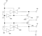
図11においては、図9、図10における補正回路901のブロック図及び回路図について示す。補正回路901は検査回路106より接続端子116に出力される信号を一定期間保持するためのメモリ回路1101、メモリ回路からの信号を反転させるための第1のインバータ回路1102、書き込み制御信号を制御するための信号SWEWEと第1のインバータ回路の出力の否定論理積を取るためのNAND回路1103、NAND回路1103の出力信号を反転させるための第2のインバータ回路1104、第2のインバータ回路からの出力を反転させるための第3のインバータ回路1105と、第2のインバータ回路1104からの出力及び第3のインバータ回路1105からの出力により制御されるアナログスイッチ1106、及び第2のインバータ回路からの信号により制御されるトランジスタ1107を有する。またNAND回路1103の出力端子の節点をN(NAND)とする。
FIG. 11 shows a block diagram and a circuit diagram of the
メモリ回路1101は信号切り替え回路1101A、信号保持回路1101Bを有する。信号切り替え回路1101Aは、検査回路106からの信号の入力または非入力を切り替える回路である。また信号保持回路1101Bは、信号切り替え回路1101Aからの出力を一定期間保持する回路である。なお、信号切り替え回路1101Aの入力端子の節点をN(116)、信号保持回路1101Bの入力端子の節点をN(in)、信号保持回路1101Bの出力端子の節点をN(out)とする。
The
また、補正回路901には書き込み制御信号SWEが入力されている。補正回路901において書き込み制御信号SWEは、信号切り替え回路1101A、信号保持回路1101B、アナログスイッチ1106の入力端子に入力される。
In addition, the write control signal SWE is input to the
また、本実施の形態においてトランジスタ1107はNチャネル型トランジスタであり、第2のインバータ回路1104からの出力は当該トランジスタ1107のゲートに出力される。そして第2のインバータ回路1104からの信号がLow信号であるとき、トランジスタ1107はオフ、アナログスイッチ1106がオンし、アナログスイッチ1106の出力端子より書き込み制御信号がソース信号線駆動回路に出力される。また、第2のインバータ回路1104からの信号がHigh信号であるとき、アナログスイッチ1106がオフ、トランジスタ1107がオンし、トランジスタ1107の第1端子に接続されたGND電位がトランジスタ1107の第2端子よりソース信号線駆動回路に出力される。
In this embodiment, the
なお本明細書において、トランジスタとは、それぞれ、ゲートと、ドレインと、ソースとを含む少なくとも三つの端子を有する素子であり、ドレイン領域とソース領域の間にチャネル領域を有する。ここで、ソースとドレインとは、トランジスタの構造や動作条件等によって変わるため、いずれがソースまたはドレインであるかを限定することが困難である。そこで、本発明においては、ソース及びドレインとして機能する領域を、それぞれ第1端子、第2端子と表記する。トランジスタにおいて、ゲートとは、ゲート電極とゲート配線(ゲート線またはゲート信号線等とも言う)とを含んだ全体、もしくは、それらの一部のことを言う。なお、ソースとは、ソース領域とソース電極とソース配線(ソース線またはソース信号線等とも言う)とを含んだ全体、もしくは、それらの一部のことを言う。なお、ドレインについては、ソースと同様である。 Note that in this specification, a transistor is an element having at least three terminals including a gate, a drain, and a source, and has a channel region between the drain region and the source region. Here, since the source and the drain vary depending on the structure and operating conditions of the transistor, it is difficult to limit which is the source or the drain. Therefore, in the present invention, regions functioning as a source and a drain are referred to as a first terminal and a second terminal, respectively. In a transistor, a gate refers to the whole or part of a gate electrode and a gate wiring (also referred to as a gate line, a gate signal line, or the like). Note that a source refers to the whole or part of a source region, a source electrode, and a source wiring (also referred to as a source line, a source signal line, or the like). The drain is the same as the source.
次に図22においては、図11における信号切り替え回路1101A、信号保持回路1101Bの回路構成について述べる。なお、図22に示す回路構成はあくまで一例であってこれに限定されないことを付記する。
Next, in FIG. 22, circuit configurations of the
図22(A)は、図11における信号切り替え回路1101Aの一例であり、インバータ回路2201、アナログスイッチ2202、トランジスタ2203を有する。図22(A)におけるトランジスタ2203はNチャネル型トランジスタであり、インバータ回路2201を介して書き込み制御信号SWEがトランジスタ2203のゲートに出力される。そして書き込み制御信号SWEの信号がHigh信号であるとき、トランジスタ2203はオフ、アナログスイッチ2202がオンし、アナログスイッチ2202の出力端子より節点N(116)の電位が節点N(in)に出力される。また、書き込み制御信号SWEの信号がLow信号であるとき、アナログスイッチ2202がオフ、トランジスタ2203がオンし、トランジスタ2203の第1端子よりGND電位がトランジスタ2203の第2端子より節点N(in)に出力される。
FIG. 22A is an example of the
図22(B)は、図11における信号保持回路1101Bの一例であり、端子Q、端子QB、端子CLK、端子D、端子XRを有するDフリップフロップ回路である。そして図22(B)’は図22(B)のDフリップフロップ回路における回路構成について示す。Dフリップフロップ回路は複数のNAND回路により構成されている。また、図22(B)におけるDフリップフロップ回路において、端子Qは節点N(out)に接続され、端子QBは端子Dに接続され、端子CLKは節点N(in)に接続され、端子XRに書き込み制御信号が入力されている。
FIG. 22B is an example of the
また、図22(C)には、図22(B)で示したDフリップフロップ回路の基本的な動作について説明する。端子CLKに入力される信号の立ち上がりにおいて、端子Qの電位がHigh電位及び端子QBの電位がLow電位に切り替わる。そして端子Q及び端子QBの電位は、次の端子CLKにおける電位の立ち上がり、または端子XRにLow電位が入力されるまで電位が保持される。 FIG. 22C illustrates a basic operation of the D flip-flop circuit illustrated in FIG. At the rise of the signal input to the terminal CLK, the potential of the terminal Q is switched to the high potential and the potential of the terminal QB is switched to the low potential. The potentials of the terminal Q and the terminal QB are held until the potential rises at the next terminal CLK or until the Low potential is input to the terminal XR.
次に図10、図11の具体的な動作について、図12に示すタイミングチャート等を用いて説明する。 Next, specific operations in FIGS. 10 and 11 will be described with reference to a timing chart shown in FIG.
図12に示すタイミングチャートは、書き込み制御信号SWE、書き込み制御信号を制御するための信号SWEWE、節点N(out)、節点N(NAND)、接続端子114、接続端子116、節点N(in)、ソースラインの電位SL、ゲートラインの電位GLの各信号及び各配線の電位についてのタイミングチャートである。なお図12におけるソースラインの電位SL、ゲートラインの電位GLは互いの電位関係をも示すものであり、ここでは通常GLの電位よりもSLの電位の方が高いと読み取れ得るものとする。図12において、書き込み制御信号SWEは、書き込み制御信号を制御するための信号SWEWEがLow電位であるときソースラインの電位SLに書き込み制御信号SWEの電位が反映され、書き込み制御信号を制御するための信号SWEWEがHigh電位であるときソースラインの電位SLに書き込み制御信号SWEの電位が反映されない。そのためソースラインの電位は書き込み制御信号を制御するための信号SWEWEがHigh電位のとき降下する。そしてソースラインの電位SLが第1のトランジスタ201の閾値電圧(Vth)の分を下回ると上述の検査回路106よりHigh電位が出力され、接続端子116の電位が上昇する。そして接続端子116の電位が上昇することにより、補正回路901が動作して書き込み制御信号がHigh電位の時の電位をソースラインが取り込むことによって、ソースラインの電位SLはゲートラインの電位GLを下回る前に上昇させることができる。そのため、ソースラインの電位SLがゲートラインの電位を下回る際に出力される接続端子114のHigh電位は検出されることはない。すなわち表示装置は良好な表示を保持することができる。なお、接続端子116の電位は、書き込み制御信号SWEの出力波形の一波長分の長さより画素部及び検査回路を経由している分遅延しているため、書き込み制御信号SWEの電位を保持することができ、補正回路901は検査回路のHigh電位を用いて補正を行うことができる。
The timing chart shown in FIG. 12 includes a write control signal SWE, a signal SWEWE for controlling the write control signal, a node N (out), a node N (NAND), a
図12において、上述の検査回路の回路を説明したように、検査回路106における第1の回路111より出力される信号が接続端子114でHigh電位を検出した際には、ソースラインの電位SLがゲートラインの電位GLを下回ったときである。また、第2の回路112に入力される基準となる電位は、実施の形態1で示した図8における矢印801で示される。このときソースラインの電位SLから第1のトランジスタ201の閾値電圧(Vth)分である矢印801の電位差を減算した電位をゲートラインの電位GLが下回った際は、接続端子116からHigh電位が出力される。
In FIG. 12, as described above for the inspection circuit, when the signal output from the
その結果、検査回路106の出力である第1の回路111から接続端子114への出力によっては、補正回路901により常に補正することでソースラインの電位SLがゲートラインの電位GLを下回ることなく、表示を良好に行うことができる。また補正は、第3の回路113から接続端子116への出力される信号にて行うことにより、表示装置に内蔵された補正回路で補正を行うことができる。もちろん実施の形態1で示した効果である表示パネルが表示中であっても、接続端子より出力されたソースラインの電位SLから画素の第1のトランジスタの閾値電圧を減算した信号を対向基板に封止された領域の外側から測定機器に接続されたプローブを用いて検査することもできる。なお、接続端子114、接続端子115、及び接続端子116は、表示を行うための映像信号やタイミング信号が入力される接続端子と同じ箇所に併設して設けても良いし、別の場所に配線を引き回しておいて、その先に接続端子を設ける構成としてもよい。
As a result, depending on the output from the
なお、本実施の形態において表示素子として発光素子を例として説明したが、ゲートライン及びソースラインによる駆動を行うアクティブマトリクス型の表示装置において、表示を行う表示素子であればよい。例えば、EL素子(有機EL素子、無機EL素子又は有機物及び無機物を含むEL素子)、電子放出素子、液晶素子、電子インク、グレーティングライトバルブ(GLV)、プラズマディスプレイパネル(PDP)、デジタルマイクロミラーデバイス(DMD)、圧電セラミックディスプレイ、カーボンナノチューブ、など、電気磁気的作用によりコントラストが変化する表示媒体を表示素子として適用することができる。なお、EL素子を用いた表示装置としてはELディスプレイ、電子放出素子を用いた表示装置としてはフィールドエミッションディスプレイ(FED)やSED方式平面型ディスプレイ(SED:Surface−conduction Electron−emitter Disply)など、液晶素子を用いた表示装置としては液晶ディスプレイ、電子インクを用いた表示装置としては電子ペーパーがある。 Note that although a light-emitting element is described as an example of a display element in this embodiment mode, any display element that performs display in an active matrix display device that is driven by a gate line and a source line may be used. For example, EL elements (organic EL elements, inorganic EL elements or EL elements including organic and inorganic substances), electron emitting elements, liquid crystal elements, electronic ink, grating light valves (GLV), plasma display panels (PDP), digital micromirror devices A display medium whose contrast is changed by an electromagnetic action, such as (DMD), a piezoelectric ceramic display, or a carbon nanotube, can be used as a display element. Note that a display device using an EL element is an EL display, and a display device using an electron-emitting device is a liquid crystal display such as a field emission display (FED) or a SED type flat display (SED: Surface-conduction Electron-Emitter Display). There is a liquid crystal display as a display device using an element, and an electronic paper as a display device using electronic ink.
なお、本実施の形態は、本明細書中の他の実施の形態と適宜組み合わせて実施することが可能である。
(実施の形態3)
Note that this embodiment can be implemented in combination with any of the other embodiments in this specification as appropriate.
(Embodiment 3)
本実施の形態においては、上記実施の形態とは別の構成について説明する。なお、実施の形態1、実施の形態2と同一の機能を有する構成については同じ符号を付し、実施の形態1、実施の形態2の説明を援用する。
In this embodiment, a structure different from the above embodiment will be described. In addition, about the structure which has the same function as Embodiment 1 and
図13に本実施の形態における表示装置のブロック図について示し、以下詳細に説明する。なお本発明において表示装置とは、表示素子(液晶素子や発光素子など)を有する装置のことを言う。なお、基板上に液晶素子やEL素子などの表示素子を含む複数の画素やそれらの画素を駆動させる周辺駆動回路が形成された表示パネル本体のことでもよい。さらに、フレキシブルプリントサーキット(FPC)やプリント配線基盤(PWB)が取り付けられたものも含んでもよい。また、発光装置とは、特にEL素子やFEDで用いる素子などの自発光型の表示素子を有している表示装置をいう。液晶表示装置とは、液晶素子を有している表示装置をいう。 FIG. 13 shows a block diagram of a display device in this embodiment mode, which will be described in detail below. Note that in the present invention, a display device refers to a device having a display element (such as a liquid crystal element or a light-emitting element). Note that a display panel body in which a plurality of pixels including a display element such as a liquid crystal element or an EL element and a peripheral driver circuit for driving these pixels are formed over a substrate may be used. Furthermore, the display device may include one provided with a flexible printed circuit (FPC) or a printed wiring board (PWB). A light-emitting device refers to a display device including a self-luminous display element such as an EL element or an element used in an FED. A liquid crystal display device refers to a display device having a liquid crystal element.
図13に本実施の形態の構成について示す。図13に示す表示装置は、基板100上に、ゲート信号線駆動回路101、ソース信号線駆動回路102、画素部103、及び複数の接続端子104が形成された接続端子部105、検査回路126、切り替え回路1301を有する。ゲート信号線駆動回路101にはゲートライン107、ソース信号線駆動回路102にはソースライン108が接続されている。画素部103における画素109は、ゲートライン107、ソースライン108に接続されている。そして、画素109には、ソースライン108からの信号をゲートライン107の信号により画素に設けられた発光素子または液晶素子に信号を書き込むためのトランジスタが設けられており、それぞれの画素においてトランジスタの各端子はゲートライン107、ソースライン108に接続されている。また、接続端子部105には、外部からの信号を入力するためのFPC(Frexible Printed Circuit:フレキシブルプリントサーキット、図示せず)が接続される。そして基板100は、画素109に設けられた発光素子または液晶素子を封止するための対向基板110を貼り付けることにより、表示モジュールとして完成する。
FIG. 13 shows the configuration of this embodiment. A display device illustrated in FIG. 13 includes a gate signal
切り替え回路1301は、ゲートライン107、ソースライン108がゲート信号線駆動回路101、ソース信号線駆動回路102と接続された反対側に設けられ、ゲートライン107、ソースライン108と接続される。なお、切り替え回路1301は、切り替え回路1301に入力される書き込み制御信号を制御するための信号SWEWE、及び検査回路106に接続端子1302から定電位の信号が入力される。そして切り替え回路1301は、検査回路106において非検査時には接続端子1302から定電位の信号を検査回路に出力し、検査回路106においてゲートライン及びソースラインの電位の検査を行う際には、ゲートラインの電位及びソースラインの電位に出力するように切り替えて検査回路に信号を出力する。
The
なお、図13において書き込み制御信号SWE(ソース ライト イネーブル信号)とは、ソースラインの信号の書き込みまたは消去を選択するための信号であり、ソース信号線駆動回路に書き込み制御信号SWEのHigh電位が入力されることで、ソースラインにHigh電位が書き込まれ、ソース信号線駆動回路に書き込み制御信号SWEのLow電位が入力されることでソースラインにLow電位が書き込まれるものとする。また図13において書き込み制御信号を制御するための信号SWEWEとは、ソース信号線駆動回路に書き込み制御信号の供給を選択するための信号であり、補正回路に書き込み制御信号を制御するための信号SWEWEのLow電位が入力されることで、ソース信号線駆動回路への書き込み制御信号SWEが供給されるものとする。 Note that a write control signal SWE (source write enable signal) in FIG. 13 is a signal for selecting writing or erasing of a signal on the source line, and the High potential of the write control signal SWE is input to the source signal line driver circuit. Thus, the High potential is written to the source line, and the Low potential of the write control signal SWE is input to the source signal line driver circuit, whereby the Low potential is written to the source line. In FIG. 13, a signal SWEWE for controlling the write control signal is a signal for selecting supply of the write control signal to the source signal line driver circuit, and a signal SWEWE for controlling the write control signal to the correction circuit. It is assumed that the write control signal SWE to the source signal line driver circuit is supplied by inputting the low potential.
検査回路126は、ゲートライン107、ソースライン108がゲート信号線駆動回路101、ソース信号線駆動回路102と接続された反対側に設けられ、ゲートライン107、ソースライン108と接続される。なお、図13において切り替え回路1301を介して検査回路に接続されるゲートライン107、ソースライン108は、表示装置において表示に寄与する画素に接続されるゲートライン、ソースラインであり、この点で上記実施の形態1及び実施の形態2とは異なる。本実施の形態においては、表示に寄与する画素に接続されるソースライン、ゲートラインの電位を検査回路126において評価することにより、より正確な表示に寄与する画素の評価を行う点で上記実施の形態1及び実施の形態2より正確な検査を行うことが可能にすることができる。
The
また、検査回路126は、切り替え回路1301を介して入力される画素部におけるゲートライン107及びソースライン108の電位関係について、ソースライン108の電位がゲートライン107の電位より低く、且つ、ソースラインからの信号の書き込みをおこなうためのトランジスタの閾値電圧(Vth)未満になった場合に起因する不良を検出する。具体的に検査回路126には、ゲートライン107、ソースライン108の電位を比較しゲートライン107の電位をソースライン108の電位が下回ったときHigh電位を出力する第1の回路121(第1の比較回路ともいう)と、ソースライン108の電位から基準となる電位を減算し出力する第2の回路122と、ゲートライン107の電位を第2の回路122の出力と比較し、出力する第3の回路123が設けられている。そして検査回路106には、引き回された配線により第1の回路121で比較した結果を出力するための接続端子114、第2の回路122に基準となる電位が入力される接続端子115、第3の回路123からの信号を出力するための接続端子116の接続端子部105にそれぞれ接続される。なお第2の回路122に入力される基準となる電位とは、本明細書では、画素に設けられたソースラインからの信号の書き込みをおこなうためのトランジスタの閾値電圧(Vth)とほぼ同じ電位が望ましく、0.1〜2.0V程度であることが望ましい。
In addition, the
なお、画素109の画素構成については、実施の形態1において図2、図3で示した例の説明を援用することにする。
Note that the description of the example shown in FIGS. 2 and 3 in Embodiment 1 is used for the pixel configuration of the
次に切り替え回路1301の一構成について図14を用いて説明する。
Next, one configuration of the
切り替え回路1301は、書き込み制御信号を制御するための信号SWEWEがHigh電位、すなわちソースラインに信号が供給されないときに、ゲートライン107の電位を検査回路に供給するためのアナログスイッチ1401、インバータ回路1402を有する。また、書き込み制御信号を制御するための信号SWEWEがLow電位、すなわちソースラインに信号が供給されているときに、検査回路126が誤作動を起こさないような電位を検査回路126に供給するためのトランジスタ1403を有する。また、書き込み制御信号を制御するための信号SWEWEがHigh電位、すなわちソースラインに信号が供給されないときに、ソースライン108の電位を検査回路に供給するためのアナログスイッチ1404、インバータ回路1405を有する。また、書き込み制御信号を制御するための信号SWEWEがLow電位、すなわちソースラインに信号が供給されているときに、検査回路126が誤作動を起こさないような電位を検査回路126に供給するためのトランジスタ1406を有する。
The
切り替え回路1301の動作について簡単に説明する。接続端子902より書き込み制御信号を制御するための信号SWEWEとしてHigh電位が入力される場合、切り替え回路1301ではゲートライン107、ソースライン108の電位が検査回路106にそれぞれ出力される。また、接続端子902より書き込み制御信号を制御するための信号SWEWEとしてLow電位が入力される場合、ゲートライン107に接続される検査回路106にはGND電位が入力され、ソースライン108側に接続される検査回路106には、GND電位よりも高い電位が接続端子1302より入力されている。これは、検査回路106がゲートライン107、ソースライン108に接続されていない間に、検査回路106に入力される電位がゲートライン107、ソースライン108の電位が不良であると判定するのを防止するためであり、検査回路126に入力される電位がゲートライン107、ソースライン108の電位を不良であると判定しない程度の電位であるならば良い。
The operation of the
なお、表示装置においてゲートライン107、ソースライン108に検査回路106を直接接続して検査を行うことは、ゲートライン107、ソースライン108から検査回路126に電流が流れてしまい、表示が不良になり、都合が悪い。本発明は切り替え回路により書き込み制御信号を制御するための信号がHigh電位であるソースライン非書き込み時に着目して検査を行うことで、より正確な検査を行うことができる。
Note that when a test is performed by directly connecting the
次に図15に本発明にかかる表示媒体として、各画素に有機材料を発光層に用いた発光素子を採用したものを示す。各画素には、その構成として実施の形態1において示した図2の第1のトランジスタと第2のトランジスタ、保持容量、発光素子を有する構成を示す。また図15においては、図13において述べた検査回路126における第1の回路121、第2の回路122、第3の回路123における接続について説明する。
Next, FIG. 15 shows a display medium according to the present invention in which a light emitting element using an organic material for a light emitting layer is adopted for each pixel. Each pixel has a structure including the first transistor and the second transistor in FIG. 2 described in Embodiment Mode 1, a storage capacitor, and a light-emitting element as its structure. In FIG. 15, connection in the
図15に図1の本発明の基本構成をさらに詳しく示したものである。なお、図15において図1と同一部分については同じ符号を付け、その説明について省略する。図15に示す表示装置は、基板上(図示せず)に、ゲート信号線駆動回路101、ソース信号線駆動回路102、画素部103、及び複数の接続端子(図示せず)が形成された接続端子部(図示せず)、検査回路126を有する。ゲート信号線駆動回路101にはゲートライン107、ソース信号線駆動回路102にはソースライン108が接続されている。なおソース信号線駆動回路には、書き込み制御信号SWEが接続端子401より入力される。画素部103における画素109は、ゲートライン107、ソースライン108に接続されている。そして、画素109には、ソースライン108からの信号をゲートライン107の信号により画素に設けられた発光素子または液晶素子に信号を書き込むためのトランジスタが設けられており、それぞれの画素においてトランジスタの各端子はゲートライン107、ソースライン108に接続されている。そして基板100は、画素109に設けられた発光素子または液晶素子を封止するための対向基板(図示せず)を貼り付けることにより、表示モジュールとして完成する。
FIG. 15 shows the basic configuration of the present invention shown in FIG. 1 in more detail. In FIG. 15, the same parts as those in FIG. In the display device illustrated in FIG. 15, a gate signal
また、検査回路126は、画素部におけるゲートライン107及びソースライン108の電位関係について、ソースライン108の電位がゲートライン107の電位より低く、且つ、第1のトランジスタ201の閾値電圧(Vth)未満になった場合に起因する不良を検出する。具体的に検査回路126には、ゲートライン107、ソースライン108の電位を比較しゲートライン107の電位をソースライン108の電位が下回ったときHigh電位を出力する第1の回路121(第1の比較回路ともいう)と、ソースライン108の電位から基準となる電位を減算し出力する第2の回路122(減算回路ともいう)と、ゲートライン107の電位を第2の回路122の出力と比較し、出力する第3の回路123(第2の比較回路ともいう)が設けられている。そして検査回路126には、配線を介して第1の回路121で比較した結果を出力するための接続端子114、第2の回路122に基準となる電位が入力される接続端子115、第3の回路123からの信号を出力するための接続端子116がそれぞれ接続される。
The
図15における検査回路126において、第1の回路121にはゲートライン107、ソースライン108、及び接続端子114が接続される。また、第2の回路122には、ソースライン108、基準となる電位が入力される接続端子115、第3の回路123に接続されている。また、第3の回路123には、第2の回路122、ゲートライン107、第3の回路123から信号を出力するための接続端子116に接続されている。なお第2の回路122に入力される基準となる電位とは、本明細書では、画素に設けられた第1のトランジスタ201の閾値電圧(Vth)とほぼ同じ電位が望ましく、0.1〜2.0V程度であることが望ましい。
In the
次に図23、図24,図25において、第1の回路121、第2の回路122、第3の回路123の回路構成及び接続について説明する。
Next, with reference to FIGS. 23, 24, and 25, circuit configurations and connections of the
図23においては、図13、図15における第1の回路121のブロック図及び回路図について示す。第1の回路121はゲートライン107とソースライン108に対し、図5に示すオペアンプの非反転入力端子にゲートライン107を、反転入力端子にソースライン108を接続し、ゲートライン107の電位と、ソースライン108の電位を比較する比較回路である。第1の回路121によってゲートライン107とソースライン108の電位関係について、ソースライン108の電位がゲートライン107の電位が下回っていないかを検知することができる。ソースライン108の電位がゲートライン107の電位が下回った場合、オペアンプの出力端子からHigh電位が接続端子114に出力される。なお、第1の回路121において、オペアンプの電源で使用する負電源はゲートライン107のLow電位より2V低い電位の電源を用いることが好適である。
FIG. 23 shows a block diagram and a circuit diagram of the
次に図24においては、図13,図15における第2の回路122のブロック図及び回路図について示す。第2の回路122はオペアンプと抵抗により構成された減算回路により構成される。第2の回路122において、ソースライン108の電位は、オペアンプの非反転入力端子に接続され、接続端子115に入力される基準となる電位は、オペアンプの反転入力端子に接続される。第2の回路122は、ソースライン108の電位から基準の電位を減算した電位を第3の回路123に出力する。この時、第2の回路122における減算回路の抵抗は全て等しいことが好ましい。また、前述の基準となる電位は、画素に設けられた第1のトランジスタの閾値電圧(Vth)とほぼ同じ電位が望ましく、0.1〜2.0V程度であることが望ましい。
Next, FIG. 24 shows a block diagram and a circuit diagram of the
次に図25においては、図13、図15における第3の回路123のブロック図、及び回路図について示す。第3の回路123は、オペアンプにより構成される比較回路であり、第2の回路122の出力の電位とゲートライン107の電位を比較する。第3の回路123において、第2の回路122の出力はオペアンプの反転入力端子に接続され、ゲートライン107の電位は非反転入力端子に入力される。そしてゲートライン107の電位と第2の回路122の出力電位を比較し、第2の回路122の出力電位がゲートライン107の電位を下回った場合、オペアンプの出力端子からHigh電位が接続端子116に出力される。そしてソースライン108の電位に第1のトランジスタ201の閾値電圧(Vth)を減算した電位がゲートライン107の電位を下回る寸前を検知することができ、ゲートライン107の電位を下回る寸前を検知することができる。
Next, FIG. 25 shows a block diagram and a circuit diagram of the
なお、検査回路126の動作についても実施の形態1の検査回路106の動作と同様であるため、ここでは実施の形態1における図8の説明を援用する。
Note that the operation of the
本実施形態により、同じ基板上に検査回路126と画素部103を具備し、対向基板110により検査回路と画素部が封止された表示装置を作製することができる。本実施形態の表示装置は、接続端子114が対向基板に封止された領域の外側にあるため、表示パネルが表示中であっても、検査回路126の出力である第1の回路121から接続端子114への出力された信号を、対向基板に封止された領域の外側から測定機器に接続されたプローブを用いて表示装置の不良を検知することができる。また接続端子116は、対向基板に封止された領域の外側にあるため、表示パネルが表示中であっても、第3の回路123より出力された画素の第1のトランジスタの閾値電圧を減算した信号を、対向基板に封止された領域の外側から測定機器に接続されたプローブを用いて検査することができる。特に本実施の形態においては、実際の表示に寄与するゲートライン及びソースラインの電位を切り替え回路で切り替えながら検査回路に出力することにより検査を行うことができるため、より表示装置における正確な検査を行うことができる。なお、接続端子114、接続端子115、及び接続端子116は、表示を行うための映像信号やタイミング信号が入力される接続端子と同じ箇所に併設して設けても良いし、別の場所に配線を引き回しておいて、その先に接続端子を設ける構成としてもよい。
According to this embodiment, a display device in which the
なお、本実施の形態は、本明細書中の他の実施の形態と適宜組み合わせて実施することが可能である。
(実施の形態4)
Note that this embodiment can be implemented in combination with any of the other embodiments in this specification as appropriate.
(Embodiment 4)
本実施の形態においては、上記実施の形態とは別の構成について説明する。なお、実施の形態1乃至実施の形態3と同一の機能を有する構成については同じ符号を付し、実施の形態1乃至実施の形態3の説明を援用する。 In this embodiment, a structure different from the above embodiment will be described. Note that components having the same functions as those of the first to third embodiments are denoted by the same reference numerals, and the description of the first to third embodiments is incorporated.
図16に本実施の形態における表示装置のブロック図について示し、以下詳細に説明する。なお本発明において表示装置とは、表示素子(液晶素子や発光素子など)を有する装置のことを言う。なお、基板上に液晶素子やEL素子などの表示素子を含む複数の画素やそれらの画素を駆動させる周辺駆動回路が形成された表示パネル本体のことでもよい。さらに、フレキシブルプリントサーキット(FPC)やプリント配線基盤(PWB)が取り付けられたものも含んでもよい。また、発光装置とは、特にEL素子やFEDで用いる素子などの自発光型の表示素子を有している表示装置をいう。液晶表示装置とは、液晶素子を有している表示装置をいう。 FIG. 16 shows a block diagram of a display device in this embodiment mode, which will be described in detail below. Note that in the present invention, a display device refers to a device having a display element (such as a liquid crystal element or a light-emitting element). Note that a display panel body in which a plurality of pixels including a display element such as a liquid crystal element or an EL element and a peripheral driver circuit for driving these pixels are formed over a substrate may be used. Furthermore, the display device may include one provided with a flexible printed circuit (FPC) or a printed wiring board (PWB). A light-emitting device refers to a display device including a self-luminous display element such as an EL element or an element used in an FED. A liquid crystal display device refers to a display device having a liquid crystal element.
図16に本実施の形態の構成について示す。図16に示す表示装置は、基板100上に、ゲート信号線駆動回路101、ソース信号線駆動回路102、画素部103、及び複数の接続端子104が形成された接続端子部105、検査回路106、補正回路901、切り替え回路1301を有する。ゲート信号線駆動回路101にはゲートライン107、ソース信号線駆動回路102にはソースライン108が接続されている。画素部103における画素109は、ゲートライン107、ソースライン108に接続されている。そして、画素109には、ソースライン108からの信号をゲートライン107の信号により画素に設けられた発光素子または液晶素子に信号を書き込むためのトランジスタが設けられており、それぞれの画素においてトランジスタの各端子はゲートライン107、ソースライン108に接続されている。また、接続端子部105には、外部からの信号を入力するためのFPC(Frexible Print Cercuit:フレキシブルプリントサーキット、図示せず)が接続される。そして基板100は、画素109に設けられた発光素子または液晶素子を封止するための対向基板110を貼り付けることにより、表示モジュールとして完成する。
FIG. 16 shows the configuration of this embodiment. A display device illustrated in FIG. 16 includes a gate signal
切り替え回路1301は、ゲートライン107、ソースライン108がゲート信号線駆動回路101、ソース信号線駆動回路102と接続された反対側に設けられ、ゲートライン107、ソースライン108と接続される。なお、切り替え回路1301には、接続端子1302から入力される定電位の信号、及び書き込み制御信号を制御するための信号SWEWEが入力される。そして切り替え回路1301は、検査回路126において非検査時には接続端子1302から定電位の信号を検査回路に出力し、検査回路126においてゲートライン及びソースラインの電位の検査を行う際には、ゲートラインの電位及びソースラインの電位に出力するように切り替えて検査回路に信号を出力する。
The
なお、図16において書き込み制御信号SWE(ソース ライト イネーブル信号)とは、ソースラインの信号の書き込みまたは消去を選択するための信号であり、ソース信号線駆動回路に書き込み制御信号SWEのHigh電位が入力されることで、ソースラインにHigh電位が書き込まれ、ソース信号線駆動回路に書き込み制御信号SWEのLow電位が入力されることでソースラインにLow電位が書き込まれるものとする。また図13において書き込み制御信号を制御するための信号SWEWEとは、ソース信号線駆動回路に書き込み制御信号の供給を選択するための信号であり、補正回路に書き込み制御信号を制御するための信号SWEWEのLow電位が入力されることで、ソース信号線駆動回路への書き込み制御信号SWEが供給されるものとする。 Note that in FIG. 16, a write control signal SWE (source write enable signal) is a signal for selecting writing or erasing of a signal of the source line, and the High potential of the write control signal SWE is input to the source signal line driver circuit. Thus, the High potential is written to the source line, and the Low potential of the write control signal SWE is input to the source signal line driver circuit, whereby the Low potential is written to the source line. In FIG. 13, a signal SWEWE for controlling the write control signal is a signal for selecting supply of the write control signal to the source signal line driver circuit, and a signal SWEWE for controlling the write control signal to the correction circuit. It is assumed that the write control signal SWE to the source signal line driver circuit is supplied by inputting the low potential.
検査回路126は、ゲートライン107、ソースライン108がゲート信号線駆動回路101、ソース信号線駆動回路102と接続された反対側に設けられ、ゲートライン107、ソースライン108と接続される。なお、図16において切り替え回路1301を介して検査回路に接続されるゲートライン107、ソースライン108は、表示装置において表示に寄与する画素に接続されるゲートライン、ソースラインであり、この点で上記実施の形態1及び実施の形態2とは異なる。本実施の形態においては、表示に寄与する画素に接続されるソースライン、ゲートラインの電位を検査回路126において評価することにより、より正確な表示に寄与する画素の評価を行う点で上記実施の形態1及び実施の形態2より正確な検査を行うことが可能にすることができる。その上で本実施の形態においては、さらに補正回路901により、ソースラインの電位の補正を行うことができる。
The
また、検査回路126は、画素部におけるゲートライン107及びソースライン108の電位関係について、ソースライン108の電位がゲートライン107の電位より低く、且つ、ソースライン108のLow電位とゲートライン107のLow電位との差がソースラインからの信号の書き込みをおこなうためのトランジスタの閾値電圧(Vth)分の値未満になった場合に起因する不良を検出する。具体的に検査回路126には、ゲートライン107、ソースライン108の電位を比較し、ゲートライン107の電位をソースライン108の電位が下回ったときHigh電位を出力する第1の回路121(第1の比較回路ともいう)と、ソースライン108の電位から基準となる電位を減算し、出力する第2の回路122(減算回路ともいう)と、ゲートライン107の電位を第2の回路122の出力と比較し、出力する第3の回路123(第2の比較回路ともいう)が設けられている。そして検査回路126には、引き回された配線により、第1の回路121で比較した結果を出力するための接続端子114、第2の回路122に基準となる電位が入力される接続端子115、第3の回路123からの信号を出力するための接続端子116の接続端子部105にそれぞれ接続される。なお第2の回路122に入力される基準となる電位とは、本明細書では、画素に設けられたソースラインからの信号の書き込みをおこなうためのトランジスタの閾値電圧(Vth)とほぼ同じ電位が望ましく、0.1〜2.0V程度であることが望ましい。
The
また、補正回路901は、検査回路126から接続端子116に引き回される配線、接続端子401、接続端子902に接続されている。なお、検査回路126に接続された接続端子116には第3の回路123より出力された信号が入力され、接続端子401には書き込み制御信号SWEが入力され、接続端子902には書き込み制御信号を制御するための信号SWEWEが入力されている。そして補正回路901により制御される書き込み制御信号が、ソース信号線駆動回路に入力される。
Further, the
なお、図16において書き込み制御信号SWE(ソース ライト イネーブル信号)とは、ソースラインの信号の書き込みまたは消去を選択するための信号であり、ソース信号線駆動回路102に書き込み制御信号SWEのHigh電位が入力されることで、ソースラインにHigh電位が書き込まれ、ソース信号線駆動回路102に書き込み制御信号SWEのLow電位が入力されることでソースラインにLow電位が書き込まれるものとする。また図16において書き込み制御信号を制御するための信号SWEWEとは、ソース信号線駆動回路に書き込み制御信号の供給を選択するための信号であり、補正回路に書き込み制御信号を制御するための信号SWEWEのLow電位が入力されることで、ソース信号線駆動回路への書き込み制御信号SWEが供給されるものとする。また、補正回路に書き込み制御信号を制御するための信号SWEWEのHigh電位が入力されることで、ソース信号線駆動回路への書き込み制御信号SWEの出力が供給、または停止か選択するものであるとする。
Note that a write control signal SWE (source write enable signal) in FIG. 16 is a signal for selecting writing or erasing of a signal on the source line, and the high potential of the write control signal SWE is supplied to the source signal
なお、画素109の画素構成については、実施の形態1において図2、図3で示した例の説明を援用することにする。
Note that the description of the example shown in FIGS. 2 and 3 in Embodiment 1 is used for the pixel configuration of the
次に図17において、図16において述べた検査回路126における第1の回路121、第2の回路122、第3の回路123における接続について説明する。なお、図17においては、図4と同様に表示媒体として、各画素に有機材料を発光層に用いた発光素子を採用し、第1のトランジスタと第2のトランジスタ、保持容量、発光素子を有する構成として説明するものとし、本実施の形態においては、以下同様の説明として述べる。なお、第1の回路121、第2の回路122、及び第3の回路123の回路構成については、実施の形態3において図23、図24、図25を用いて示した例の説明を援用する。その構成とて図2で示した第1のトランジスタと第2のトランジスタ、保持容量、発光素子を有する構成を示す。
Next, in FIG. 17, connections in the
図17に図16の本発明の基本構成をさらに詳しく示したものである。なお、図17において図16と同一部分については同じ符号を付け、その説明について省略する。図17に示す表示装置は、基板上(図示せず)に、ゲート信号線駆動回路101、ソース信号線駆動回路102、画素部103、及び複数の接続端子(図示せず)が形成された接続端子部(図示せず)、検査回路126、補正回路901、切り替え回路1301を有する。ゲート信号線駆動回路101にはゲートライン107、ソース信号線駆動回路102にはソースライン108が接続されている。なおソース信号線駆動回路には、書き込み制御信号SWEが接続端子401より入力される。画素部103における画素109は、ゲートライン107、ソースライン108に接続されている。そして、画素109には、ソースライン108からの信号をゲートライン107の信号により画素に設けられた発光素子または液晶素子に信号を書き込むためのトランジスタが設けられており、それぞれの画素においてトランジスタの各端子はゲートライン107、ソースライン108に接続されている。そして基板は、画素109に設けられた発光素子または液晶素子を封止するための対向基板(図示せず)を貼り付けることにより、表示モジュールとして完成する。
FIG. 17 shows the basic configuration of the present invention shown in FIG. 16 in more detail. In FIG. 17, the same parts as those in FIG. 17 is a connection in which a gate signal
また、検査回路126は、画素部におけるゲートライン107及びソースライン108の電位関係について、ソースライン108の電位がゲートライン107の電位より低く、且つ、第1のトランジスタ201の閾値電圧(Vth)未満になった場合に起因する不良を検出する。具体的に検査回路には、ゲートライン107、ソースライン108の電位を比較しゲートライン107の電位をソースライン108の電位が下回ったときHigh電位を出力する第1の回路121(第1の比較回路ともいう)と、ソースライン108の電位から基準となる電位を減算し出力する第2の回路122(減算回路ともいう)と、ゲートライン107の電位を第2の回路122の出力と比較し出力する第3の回路123(第2の比較回路ともいう)が設けられている。そして検査回路126には、引き回された配線により、第1の回路121で比較した結果を出力するための接続端子114、第2の回路122に基準となる電位が入力される接続端子115、第3の回路123からの信号を出力するための接続端子116の接続端子部105にそれぞれ接続される。
The
図17における検査回路126において、第1の回路121にはゲートライン107、ソースライン108、及び接続端子114が接続される。また、第2の回路122には、ソースライン108、基準となる電位が入力される接続端子115、第3の回路123に接続されている。また、第3の回路123には、第2の回路122、ゲートライン107、第3の回路123から信号を出力するための接続端子116が接続されている。なお第2の回路122に入力される基準となる電位とは、本明細書では、画素に設けられた第1のトランジスタ201の閾値電圧(Vth)とほぼ同じ電位が望ましく、0.1〜2.0V程度であることが望ましい。
In the
また、補正回路901は、検査回路126から接続端子116に引き回される配線、接続端子401、接続端子902に接続されている。なお、検査回路126に接続された接続端子116には第3の回路123より出力された信号が入力され、接続端子401には書き込み制御信号SWEが入力され、接続端子902には書き込み制御信号を制御するための信号SWEWEが入力されている。そして補正回路901により制御される書き込み制御信号が、ソース信号線駆動回路102に入力される。
Further, the
なお、図17において書き込み制御信号SWE(ソース ライト イネーブル信号)とは、ソースラインの信号の書き込みまたは消去を選択するための信号であり、ソース信号線駆動回路に書き込み制御信号SWEのHigh電位が入力されることで、ソースラインにHigh電位が書き込まれ、ソース信号線駆動回路に書き込み制御信号SWEのLow電位が入力されることでソースラインにLow電位が書き込まれるものとする。また、図17において書き込み制御信号を制御するための信号SWEWEとは、ソース信号線駆動回路に書き込み制御信号の供給を選択するための信号であり、補正回路に書き込み制御信号を制御するための信号SWEWEのLow電位が入力されることで、ソース信号線駆動回路への書き込み制御信号SWEが供給されるものとする。また、補正回路に書き込み制御信号を制御するための信号SWEWEのHigh電位が入力されることで、ソース信号線駆動回路への書き込み制御信号SWEの出力が供給、または停止が選択されるものであるとする。 Note that in FIG. 17, a write control signal SWE (source write enable signal) is a signal for selecting writing or erasing of a signal of the source line, and the High potential of the write control signal SWE is input to the source signal line driver circuit. Thus, the High potential is written to the source line, and the Low potential of the write control signal SWE is input to the source signal line driver circuit, whereby the Low potential is written to the source line. In FIG. 17, a signal SWEWE for controlling the write control signal is a signal for selecting supply of the write control signal to the source signal line driver circuit, and a signal for controlling the write control signal to the correction circuit. It is assumed that the write control signal SWE to the source signal line driver circuit is supplied by inputting the low potential of SWEWE. Further, when the High potential of the signal SWEWE for controlling the write control signal is input to the correction circuit, the output of the write control signal SWE to the source signal line driver circuit is selected to be supplied or stopped. And
なお、本実施の形態においては、検査回路126における第1の回路121、第2の回路122、及び第3の回路123の回路構成については、実施の形態3において図23、図24、図25を用いて示した例の説明を援用する。また補正回路901の回路構成については、実施の形態2について図11、図22を用いて示した例の説明を援用する。また検査回路126の動作についても実施の形態1の検査回路106の動作と同様であるためここでは実施の形態1における図8の説明を援用する。また補正回路901の動作についても実施の形態2と同様であるため、ここでは実施の形態2における図12の説明を援用する。
Note that in this embodiment, the circuit configurations of the
その結果、検査回路126の出力である第1の回路121から接続端子114への出力は、補正回路901により常に補正することでソースラインの電位SLがゲートラインの電位を下回ることなく、表示を良好に行うことができる。また補正は、第3の回路123から接続端子116への出力される信号にて行うことにより、表示装置に内蔵された補正回路901で補正を行うことができる。もちろん実施の形態1で示した効果である表示パネルが表示中であっても接続端子に出力されたソースラインの電位SLから画素の第1のトランジスタの閾値電圧を減算した信号を対向基板に封止された領域の外側から測定機器に接続されたプローブを用いて検査することもできる。特に本発明の実施の形態においては、実際の表示に寄与するゲートライン及びソースラインの電位を切り替え回路1301で切り替えながら検査回路126に出力することにより検査を行うことができるため、より表示装置における正確な表示を行うことができる。なお、接続端子114、接続端子115、及び接続端子116は、表示を行うための映像信号やタイミング信号が入力される接続端子と同じ箇所に併設して設けても良いし、別の場所に新たに配線を引き回しておいて、その先に新たに接続端子を設ける構成としてもよい。
As a result, the output from the
なお、本実施の形態は、本明細書中の他の実施の形態と適宜組み合わせて実施することが可能である。 Note that this embodiment can be implemented in combination with any of the other embodiments in this specification as appropriate.
本発明の表示装置が有する画素は、実施の形態1で示した図2に示す構成に限定されない。図18(A)に、本発明の表示装置が有する画素の一形態を示す。図18に示す画素は、発光素子1801と、スイッチング用トランジスタ1802と、駆動用トランジスタ1803と、発光素子1801への電流の供給の有無を選択する電流制御用トランジスタ1804とを有している。さらに図18(A)には示されていないが、ビデオ信号の電圧を保持するための容量素子を画素に形成しても良い。
The pixel included in the display device of the present invention is not limited to the structure shown in FIG. FIG. 18A illustrates one mode of a pixel included in the display device of the present invention. The pixel shown in FIG. 18 includes a light-emitting
駆動用トランジスタ1803及び電流制御用トランジスタ1804は、同じ極性であっても異なる極性であってもどちらでも良い。駆動用トランジスタ1803は飽和領域で動作させ、電流制御用トランジスタ1804は線形領域で動作させる。なお駆動用トランジスタ1803は飽和領域で動作させることが望ましいが、本発明は必ずしもこの構成に限定されず、駆動用トランジスタ1803を線形領域で動作させても良い。また、スイッチング用トランジスタ1802は線形領域で動作させる。スイッチング用トランジスタ1802は、nチャネル型であってもpチャネル型であってもどちらでも良い。
The driving
図18(A)のように、駆動用トランジスタ1803がp型の場合、発光素子1801の陽極を第1の電極とし、陰極を第2の電極として用いるのが好ましい。逆に駆動用トランジスタ1803がn型の場合、発光素子1801の陰極を第1の電極とし、陽極を第2の電極として用いるのが好ましい。
As shown in FIG. 18A, in the case where the driving
スイッチング用トランジスタ1802のゲートは、走査線Gj(j=1〜y)に接続されている。スイッチング用トランジスタ1802のソースとドレインは、一方が信号線Si(i=1〜x)に、もう一方が電流制御用トランジスタ1804のゲートに接続されている。駆動用トランジスタ1803のゲートは電源線Vi(i=1〜x)に接続されている。そして駆動用トランジスタ1803及び電流制御用トランジスタ1804は、電源線Viから供給される電流が、駆動用トランジスタ1803及び電流制御用トランジスタ1804のドレイン電流として発光素子1801に供給されるように、電源線Vi、発光素子1801と接続されている。本実施の形態では、駆動用トランジスタ1803のソースが電源線Viに接続され、駆動用トランジスタ1803と発光素子1801の第1の電極との間に、電流制御用トランジスタ1804が設けられている。
The gate of the
容量素子を形成する場合、該容量素子が有する2つの電極は、一方が電源線Viに接続され、もう一方が電流制御用トランジスタ1804のゲートに接続されるようにする。容量素子は、電流制御用トランジスタ1804のゲート電圧を保持するために設けられている。
In the case of forming a capacitor element, one of the two electrodes included in the capacitor element is connected to the power supply line Vi and the other electrode is connected to the gate of the
なお、図18(A)に示す画素の構成は、本発明の一形態を示したに過ぎず、本発明の発光装置は図18(A)に限定されない。例えば図18(B)に示すように、駆動用トランジスタ1803のドレイン端子を発光素子1801の第1の電極に接続し、駆動用トランジスタ1803と電源線Viの間に電流制御用トランジスタ1804を形成しても良い。なお図18(B)では、図18(A)において既に示したものに同じ符号を付す。
Note that the structure of the pixel illustrated in FIG. 18A is merely one embodiment of the present invention, and the light-emitting device of the present invention is not limited to FIG. For example, as shown in FIG. 18B, the drain terminal of the driving
なお、本実施例は、本明細書中の実施の形態及び他の実施例と適宜組み合わせて実施することが可能である。 Note that this embodiment can be implemented in combination with any of the embodiment modes and other embodiments in this specification as appropriate.
本発明の表示装置は、対向基板により封止した後において、表示不良を検査しつつ、且つ補正することで歩留まりをあげることができるので、携帯電話、携帯型ゲーム機または電子書籍、ビデオカメラやデジタルスチルカメラといったカメラ等の、大量生産される電子機器が有する表示部として用いるのに最適である。 Since the display device of the present invention can increase the yield by inspecting and correcting display defects after sealing with the counter substrate, the mobile phone, the portable game machine or the electronic book, the video camera, It is most suitable for use as a display portion of a mass-produced electronic device such as a digital still camera.
その他、本発明の表示装置を用いることができる電子機器として、ビデオカメラ、デジタルカメラ、ゴーグル型ディスプレイ(ヘッドマウントディスプレイ)、ナビゲーションシステム、音響再生装置(カーオーディオ、オーディオコンポ等)、ノート型パーソナルコンピュータ、ゲーム機器、記録媒体を備えた画像再生装置(代表的にはDVD:Digital Versatile Disc等の記録媒体を再生し、その画像を表示しうるディスプレイを有する装置)などが挙げられる。これら電子機器の具体例を図19に示す。 Other electronic devices that can use the display device of the present invention include a video camera, a digital camera, a goggle type display (head mounted display), a navigation system, a sound reproduction device (car audio, audio component, etc.), and a notebook type personal computer. And an image playback device (typically, a device having a display that can play back a recording medium such as a DVD: Digital Versatile Disc and display the image). Specific examples of these electronic devices are shown in FIGS.
図19(A)は携帯電話であり、本体1901、表示部1902、音声入力部1903、音声出力部1904、操作キー1905を含む。本発明の表示装置を表示部1902に用いることにより、本発明の電子機器の一つである携帯電話を完成させることができる。
FIG. 19A illustrates a mobile phone, which includes a
図19(B)はビデオカメラであり、本体1906、表示部1907、筐体1908、外部接続ポート1909、リモコン受信部1910、受像部1911、バッテリー1912、音声入力部1913、操作キー1914、接眼部1915等を含む。本発明の表示装置を表示部1907に用いることにより、本発明の電子機器の一つであるビデオカメラを完成させることができる。
FIG. 19B illustrates a video camera, which includes a
図19(C)は表示ディスプレイであり、筐体1916、表示部1917、スピーカー部1918等を含む。本発明の表示装置を表示部1917に用いることにより、本発明の電子機器の一つである表示ディスプレイを完成させることができる。なお、表示ディスプレイには、パーソナルコンピュータ用、TV放送受信用、広告表示用などの全ての情報表示用表示装置が含まれる。
FIG. 19C illustrates a display, which includes a
以上の様に、本発明の適用範囲は極めて広く、あらゆる分野の電子機器に用いることが可能である。 As described above, the applicable range of the present invention is so wide that it can be used for electronic devices in various fields.
なお、本実施例は、本明細書中の実施の形態及び他の実施例と適宜組み合わせて実施することが可能である。 Note that this embodiment can be implemented in combination with any of the embodiment modes and other embodiments in this specification as appropriate.
100 基板
101 ゲート信号線駆動回路
102 ソース信号線駆動回路
103 画素部
104 接続端子
105 接続端子部
106 検査回路
107 ゲートライン
108 ソースライン
109 画素
110 対向基板
111 第1の回路
112 第2の回路
113 第3の回路
114 接続端子
115 接続端子
116 接続端子
117 ダミーのゲートライン
118 ダミーのソースライン
121 第1の回路
122 第2の回路
123 第3の回路
126 検査回路
201 第1のトランジスタ
202 第2のトランジスタ
203 保持容量
204 電源線
205 発光素子
206 対向電極
301 トランジスタ
302 保持容量
303 液晶素子
304 対向電極
401 接続端子
901 補正回路
902 接続端子
1101 メモリ回路
1102 インバータ回路
1103 NAND回路
1104 インバータ回路
1105 インバータ回路
1106 アナログスイッチ
1107 トランジスタ
1301 切り替え回路
1302 接続端子
1401 アナログスイッチ
1402 インバータ回路
1403 トランジスタ
1404 アナログスイッチ
1405 インバータ回路
1406 トランジスタ
1801 発光素子
1802 スイッチング用トランジスタ
1803 駆動用トランジスタ
1804 電流制御用トランジスタ
1901 本体
1902 表示部
1903 音声入力部
1904 音声出力部
1905 操作キー
1906 本体
1907 表示部
1908 筐体
1909 外部接続ポート
1910 リモコン受信部
1911 受像部
1912 バッテリー
1913 音声入力部
1914 操作キー
1915 接眼部
1916 筐体
1917 表示部
1918 スピーカー部
2000 基板
2001 ゲート信号線駆動回路
2002 ソース信号線駆動回路
2003 画素部
2004 接続端子
2005 接続端子部
2006 ゲートライン
2007 ソースライン
2008 画素
2009 電源線
2010 対向基板
2101 プローブ
2201 インバータ回路
2202 アナログスイッチ
2203 トランジスタ
1101A 信号切り替え回路
1101B 信号保持回路
100 Substrate 101 Gate signal line driver circuit 102 Source signal line driver circuit 103 Pixel portion 104 Connection terminal 105 Connection terminal portion 106 Inspection circuit 107 Gate line 108 Source line 109 Pixel 110 Counter substrate 111 First circuit 112 Second circuit 113 Second 3 circuit 114 connection terminal 115 connection terminal 116 connection terminal 117 dummy gate line 118 dummy source line 121 first circuit 122 second circuit 123 third circuit 126 test circuit 201 first transistor 202 second transistor 203 Storage capacitor 204 Power supply line 205 Light emitting element 206 Counter electrode 301 Transistor 302 Storage capacitor 303 Liquid crystal element 304 Counter electrode 401 Connection terminal 901 Correction circuit 902 Connection terminal 1101 Memory circuit 1102 Inverter circuit 1103 NAN Circuit 1104 Inverter circuit 1105 Inverter circuit 1106 Analog switch 1107 Transistor 1301 Switching circuit 1302 Connection terminal 1401 Analog switch 1402 Inverter circuit 1403 Transistor 1404 Analog switch 1405 Inverter circuit 1406 Transistor 1801 Light emitting element 1802 Switching transistor 1803 Driving transistor 1804 Current control transistor 1901 Main body 1902 Display unit 1903 Audio input unit 1904 Audio output unit 1905 Operation key 1906 Main unit 1907 Display unit 1908 Case 1909 External connection port 1910 Remote control reception unit 1911 Image receiving unit 1912 Battery 1913 Audio input unit 1914 Operation key 1915 Eyepiece unit 1916 Case Body 1917 Display 1918 -Car portion 2000 substrate 2001 gate signal line drive circuit 2002 source signal line drive circuit 2003 pixel portion 2004 connection terminal 2005 connection terminal portion 2006 gate line 2007 source line 2008 pixel 2009 power supply line 2010 counter substrate 2101 probe 2201 inverter circuit 2202 analog switch 2203 transistor 1101A Signal switching circuit 1101B Signal holding circuit
Claims (10)
ソースラインと、
前記ゲートライン及び前記ソースラインの電位により駆動される画素部と、
前記ゲートラインと平行に配置された第1の配線と、
前記ソースラインと平行に配置された第2の配線と、
前記ゲートライン及び前記第1の配線に第1の信号を出力するゲート信号線駆動回路と、
前記ソースライン及び前記第2の配線に第2の信号を出力するソース信号線駆動回路と、
前記第1の配線及び前記第2の配線に接続された検査回路と、
前記検査回路に接続された第1の接続端子及び第2の接続端子と、を有し、
前記検査回路は、
前記第1の配線及び前記第2の配線に接続された第1の回路と、
前記第2の配線に接続された第2の回路と、
前記第1の配線及び前記第2の回路に接続された第3の回路と、を有し、
前記第1の回路は、帰線期間おいて、前記第1の配線の電位と前記第2の配線の電位とを比較し、前記第2の配線の電位が前記第1の配線の電位を下回った場合に第1の電位を前記第1の接続端子に出力し、
前記第2の回路は、前記第2の配線の電位から基準となる電位を減算した第2の電位を
前記第3の回路に入力し、
前記第3の回路は、前記第1の配線の電位と前記第2の電位とを比較し、前記第2の電
位が前記第1の配線の電位を下回った場合に第3の電位を前記第2の接続端子に出力する
ことを特徴とする表示装置。 The gate line,
Source line,
A pixel portion driven by a potential of the gate line and the source line;
A first wiring disposed in parallel with the gate line;
A second wiring arranged in parallel with the source line;
A gate signal line driving circuit for outputting a first signal to the gate line and the first wiring;
A source signal line driver circuit for outputting a second signal before Kiso baselines and the second wiring,
An inspection circuit connected to the first wiring and the second wiring;
A first connection terminal and a second connection terminal connected to the inspection circuit;
The inspection circuit includes:
A first circuit connected to the first wiring and the second wiring;
A second circuit connected to the second wiring;
A third circuit connected to the first wiring and the second circuit,
The first circuit compares the potential of the first wiring and the potential of the second wiring in a retrace period, and the potential of the second wiring is lower than the potential of the first wiring. A first potential is output to the first connection terminal when
The second circuit inputs a second potential obtained by subtracting a reference potential from the potential of the second wiring to the third circuit,
The third circuit compares the potential of the first wiring with the second potential, and if the second potential is lower than the potential of the first wiring, the third circuit compares the potential of the first wiring with the second potential. A display device that outputs to two connection terminals.
ソースラインと、
前記ゲートライン及び前記ソースラインの電位により駆動される画素部と、
前記ゲートラインと平行に配置された第1の配線と、
前記ソースラインと平行に配置された第2の配線と、
前記ゲートライン及び前記第1の配線に第1の信号を出力するゲート信号線駆動回路と、
前記ソースライン及び前記第2の配線に第2の信号を出力するソース信号線駆動回路と、
前記第1の配線及び前記第2の配線に接続された検査回路と、
前記検査回路に接続された補正回路と、
前記検査回路に接続された第1の接続端子及び第2の接続端子と、を有し、
前記検査回路は、
前記第1の配線及び前記第2の配線に接続された第1の回路と、
前記第2の配線に接続された第2の回路と、
前記第1の配線及び前記第2の回路に接続された第3の回路と、を有し、
前記第1の回路は、帰線期間において、前記第1の配線の電位と前記第2の配線の電位とを比較し、前記第2の配線の電位が前記第1の配線の電位を下回った場合に第1の電位を前記第1の接続端子に出力し、
前記第2の回路は、前記第2の配線の電位から基準となる電位を減算した第2の電位を
前記第3の回路に入力し、
前記第3の回路は、前記第1の配線の電位と前記第2の電位とを比較し、前記第2の電
位が前記第1の配線の電位を下回った場合に第3の電位を前記第2の接続端子に出力し、
前記補正回路は、前記第2の接続端子に前記第3の電位が出力された際に、前記第2の
配線の電位を前記第1の配線の電位よりも高くすることにより、前記第1の接続端子及び
前記第2の接続端子に出力される電位の補正を行うことを特徴とする表示装置。 The gate line,
Source line,
A pixel portion driven by a potential of the gate line and the source line;
A first wiring disposed in parallel with the gate line;
A second wiring arranged in parallel with the source line;
A gate signal line driving circuit for outputting a first signal to the gate line and the first wiring;
A source signal line driver circuit for outputting a second signal before Kiso baselines and the second wiring,
An inspection circuit connected to the first wiring and the second wiring;
A correction circuit connected to the inspection circuit;
A first connection terminal and a second connection terminal connected to the inspection circuit;
The inspection circuit includes:
A first circuit connected to the first wiring and the second wiring;
A second circuit connected to the second wiring;
A third circuit connected to the first wiring and the second circuit,
The first circuit compares the potential of the first wiring and the potential of the second wiring in a retrace period, and the potential of the second wiring is lower than the potential of the first wiring. Output a first potential to the first connection terminal,
The second circuit inputs a second potential obtained by subtracting a reference potential from the potential of the second wiring to the third circuit,
The third circuit compares the potential of the first wiring with the second potential, and if the second potential is lower than the potential of the first wiring, the third circuit compares the potential of the first wiring with the second potential. 2 to the connection terminal,
The correction circuit increases the potential of the second wiring higher than the potential of the first wiring when the third potential is output to the second connection terminal. A display device that corrects a potential output to a connection terminal and the second connection terminal.
前記第1の接続端子及び前記第2の接続端子は、前記画素部が形成される基板と対向基板により封止される領域の外側に設けられていることを特徴とする表示装置。 In claim 1 or claim 2 ,
Said first connecting terminal and the second connection terminal, a display device, characterized in that are provided outside of the region sealed by the substrate and a counter substrate on which the pixel portion is formed.
ソースラインと、
前記ソースラインに信号を供給する駆動回路と、
前記ゲートライン及び前記ソースラインの電位により駆動される画素部と、
前記ゲートライン及び前記ソースラインに接続された切り替え回路と、
検査回路と、
前記検査回路に接続された第1の接続端子及び第2の接続端子と、を有し、
前記検査回路は、
前記ゲートライン及び前記ソースラインに接続された第1の回路と、
前記ソースラインに接続された第2の回路と、
前記ゲートライン及び前記第2の回路に接続された第3の回路と、を有し、
前記切り替え回路は、帰線期間において、前記ソースラインの書き込みを制御する信号が前記駆動回路に供給されない場合に、前記ゲートライン及び前記ソースラインと前記検査回路とを接続させ、
前記第1の回路は、入力された前記ゲートラインの電位と前記より入力された電位とを
比較し、入力された前記ソースラインの電位が前記ゲートラインの電位を下回った場合に
第1の電位を前記第1の接続端子に出力し、
前記第2の回路は、入力された前記ソースラインの電位から基準となる電位を減算した
第2の電位を前記第3の回路に入力し、
前記第3の回路は、入力された前記ゲートラインの電位と前記第2の電位とを比較し、
前記第2の電位が前記ゲートラインの電位を下回った場合に第3の電位を前記第2の接続
端子に出力することを特徴とする表示装置。 The gate line,
Source line,
A drive circuit for supplying a signal to the source line;
A pixel portion driven by a potential of the gate line and the source line;
A switching circuit connected to the gate line and the source line;
An inspection circuit;
A first connection terminal and a second connection terminal connected to the inspection circuit;
The inspection circuit includes:
A first circuit connected to the gate line and the source line;
A second circuit connected to the source line;
A third circuit connected to the gate line and the second circuit,
The switching circuit is in the blanking period, when the signal for controlling the writing of the source line is not supplied to the driving circuit, is connected to the gate line and the source line and said test circuit,
The first circuit compares the inputted potential of the gate line with the inputted potential, and when the inputted potential of the source line falls below the potential of the gate line, the first potential Is output to the first connection terminal,
The second circuit inputs a second potential obtained by subtracting a reference potential from the input source line potential to the third circuit,
The third circuit compares the input potential of the gate line with the second potential,
The display device, wherein the third potential is output to the second connection terminal when the second potential is lower than the potential of the gate line.
ソースラインと、
前記ソースラインに信号を供給する駆動回路と、
前記ゲートライン及び前記ソースラインの電位により駆動される画素部と、
前記ゲートライン及び前記ソースラインに接続された切り替え回路と、
検査回路と、
前記検査回路に接続された第1の接続端子及び第2の接続端子と、
前記検査回路及び前記第2の接続端子に接続された補正回路と、を有し、
前記検査回路は、
前記ゲートライン及び前記ソースラインに接続された第1の回路と、
前記ソースラインに接続された第2の回路と、
前記ゲートライン及び前記第2の回路に接続された第3の回路と、を有し、
前記切り替え回路は、帰線期間において、前記ソースラインに書き込みを制御する信号が前記駆動回路に供給されない場合に、前記ゲートライン及び前記ソースラインと前記検査回路とを接続させ、
前記第1の回路は、入力された前記ゲートラインの電位と前記ソースラインの電位とを
比較し、前記ソースラインの電位が前記ゲートラインの電位を下回った場合に第1の電位
を前記第1の接続端子に出力し、
前記第2の回路は、入力された前記ソースラインの電位から基準となる電位を減算した
第2の電位を前記第3の回路に入力し、
前記第3の回路は、入力された前記ゲートラインの電位と前記第2の電位とを比較し、
前記第2の電位が前記ゲートラインの電位を下回った場合に第3の電位を前記第2の接続
端子に出力し、
前記補正回路は、前記第2の接続端子に前記第3の電位が出力された際に、前記ソース
ラインの電位を前記ゲートラインの電位よりも高くすることにより、前記第1の接続端子
及び前記第2の接続端子に出力される電位の補正を行うことを特徴とする表示装置。 The gate line,
Source line,
A drive circuit for supplying a signal to the source line;
A pixel portion driven by a potential of the gate line and the source line;
A switching circuit connected to the gate line and the source line;
An inspection circuit;
A first connection terminal and a second connection terminal connected to the inspection circuit;
A correction circuit connected to the inspection circuit and the second connection terminal,
The inspection circuit includes:
A first circuit connected to the gate line and the source line;
A second circuit connected to the source line;
A third circuit connected to the gate line and the second circuit,
The switching circuit connects the gate line and the source line and the inspection circuit when a signal for controlling writing to the source line is not supplied to the driving circuit in a blanking period,
The first circuit compares the input potential of the gate line and the potential of the source line, and if the potential of the source line falls below the potential of the gate line, the first potential is set to the first potential. Output to the connection terminal of
The second circuit inputs a second potential obtained by subtracting a reference potential from the input source line potential to the third circuit,
The third circuit compares the input potential of the gate line with the second potential,
When the second potential is lower than the gate line potential, a third potential is output to the second connection terminal;
The correction circuit sets the potential of the source line higher than the potential of the gate line when the third potential is output to the second connection terminal. A display device that corrects a potential output to a second connection terminal.
前記第1の接続端子及び前記第2の接続端子は、前記画素部が形成される基板と対向基板により封止される領域の外側に設けられていることを特徴とする表示装置。 In claim 4 or claim 5 ,
Said first connecting terminal and the second connection terminal, a display device, characterized in that are provided outside of the region sealed by the substrate and a counter substrate on which the pixel portion is formed.
前記画素部は、前記ゲートライン及び前記ソースラインに接続されたトランジスタを有
し、
前記トランジスタは、前記ゲートラインに入力される信号により選択され、前記ソース
ラインからの信号が書き込まれることを特徴とする表示装置。 In any one of Claims 1 thru | or 6 ,
The pixel portion includes a transistor connected to the gate line and the source line,
The transistor is selected by a signal input to the gate line, and a signal from the source line is written thereto.
前記トランジスタは、Nチャネル型トランジスタであることを特徴とする表示装置。 In claim 7 ,
The display device is characterized in that the transistor is an N-channel transistor.
前記画素部は、前記第1の配線の電位及び前記第2の配線の電位により駆動され、表示に寄与しない画素を有することを特徴とする表示装置。 In any one of Claims 1 thru | or 8 ,
The display device is characterized in that the pixel portion includes a pixel which is driven by the potential of the first wiring and the potential of the second wiring and does not contribute to display.
Priority Applications (1)
| Application Number | Priority Date | Filing Date | Title |
|---|---|---|---|
| JP2007015719A JP5127244B2 (en) | 2006-02-03 | 2007-01-26 | Display device and electronic apparatus including the display device |
Applications Claiming Priority (3)
| Application Number | Priority Date | Filing Date | Title |
|---|---|---|---|
| JP2006026761 | 2006-02-03 | ||
| JP2006026761 | 2006-02-03 | ||
| JP2007015719A JP5127244B2 (en) | 2006-02-03 | 2007-01-26 | Display device and electronic apparatus including the display device |
Publications (3)
| Publication Number | Publication Date |
|---|---|
| JP2007233353A JP2007233353A (en) | 2007-09-13 |
| JP2007233353A5 JP2007233353A5 (en) | 2010-02-12 |
| JP5127244B2 true JP5127244B2 (en) | 2013-01-23 |
Family
ID=38553951
Family Applications (1)
| Application Number | Title | Priority Date | Filing Date |
|---|---|---|---|
| JP2007015719A Expired - Fee Related JP5127244B2 (en) | 2006-02-03 | 2007-01-26 | Display device and electronic apparatus including the display device |
Country Status (1)
| Country | Link |
|---|---|
| JP (1) | JP5127244B2 (en) |
Families Citing this family (3)
| Publication number | Priority date | Publication date | Assignee | Title |
|---|---|---|---|---|
| JP5211962B2 (en) * | 2008-09-12 | 2013-06-12 | セイコーエプソン株式会社 | Display device |
| WO2011081011A1 (en) * | 2009-12-28 | 2011-07-07 | Semiconductor Energy Laboratory Co., Ltd. | Liquid crystal display device and manufacturing method thereof |
| US8947337B2 (en) | 2010-02-11 | 2015-02-03 | Semiconductor Energy Laboratory Co., Ltd. | Display device |
Family Cites Families (12)
| Publication number | Priority date | Publication date | Assignee | Title |
|---|---|---|---|---|
| JPS61256382A (en) * | 1985-05-10 | 1986-11-13 | 三菱電機株式会社 | Liquid crystal display unit |
| JP3353320B2 (en) * | 1992-02-17 | 2002-12-03 | ソニー株式会社 | Gradation correction device and laser display device |
| JP3203864B2 (en) * | 1992-03-30 | 2001-08-27 | ソニー株式会社 | Active matrix substrate manufacturing method, inspection method and apparatus, and liquid crystal display device manufacturing method |
| JPH10260391A (en) * | 1997-03-19 | 1998-09-29 | Fujitsu Ltd | Liquid crystal display device with inspecting circuit |
| JP2000020020A (en) * | 1998-06-26 | 2000-01-21 | Canon Inc | Electron source drive device, image forming device, and method for correcting electron emission characteristic of electron source |
| JP4239299B2 (en) * | 1999-06-14 | 2009-03-18 | 三菱電機株式会社 | Active matrix type liquid crystal display device |
| US6795046B2 (en) * | 2001-08-16 | 2004-09-21 | Koninklijke Philips Electronics N.V. | Self-calibrating image display device |
| JP4610886B2 (en) * | 2002-12-06 | 2011-01-12 | 株式会社半導体エネルギー研究所 | Image display device, electronic equipment |
| JP2005013661A (en) * | 2003-06-30 | 2005-01-20 | Og Giken Co Ltd | Bathing apparatus |
| JP2005043783A (en) * | 2003-07-25 | 2005-02-17 | Oht Inc | Device for inspecting liquid crystal display panel, and method for inspecting liquid crystal panel |
| JP4465183B2 (en) * | 2003-12-05 | 2010-05-19 | 株式会社半導体エネルギー研究所 | Active matrix liquid crystal display panel and defective pixel determination method thereof, element substrate for active matrix liquid crystal display panel and defective element determination method thereof |
| JP4026618B2 (en) * | 2004-05-20 | 2007-12-26 | セイコーエプソン株式会社 | Electro-optical device, inspection method thereof, and electronic apparatus |
-
2007
- 2007-01-26 JP JP2007015719A patent/JP5127244B2/en not_active Expired - Fee Related
Also Published As
| Publication number | Publication date |
|---|---|
| JP2007233353A (en) | 2007-09-13 |
Similar Documents
| Publication | Publication Date | Title |
|---|---|---|
| US8324920B2 (en) | Display device including test circuit, and electronic apparatus having the display device | |
| JP7447229B2 (en) | display device | |
| JP5740432B2 (en) | Display device | |
| CN112599055A (en) | Display device and driving method thereof | |
| TWI431588B (en) | Display device and electronic device having the same | |
| JP4966075B2 (en) | Display device | |
| JP5127244B2 (en) | Display device and electronic apparatus including the display device | |
| KR20170081046A (en) | Organic light emitting display device, data driver and sample hold circuit | |
| US11900843B2 (en) | Display device and display driving method | |
| JP4954744B2 (en) | Display device and electronic apparatus including the display device | |
| JP4869688B2 (en) | Active matrix light emitting device | |
| JP5072254B2 (en) | Display device | |
| CN118430455A (en) | Display device and driving method thereof | |
| JP5041777B2 (en) | Display device and electronic device | |
| JP4614708B2 (en) | Circuit and semiconductor device having source follower | |
| JP2007140496A (en) | Semiconductor device |
Legal Events
| Date | Code | Title | Description |
|---|---|---|---|
| RD02 | Notification of acceptance of power of attorney |
Free format text: JAPANESE INTERMEDIATE CODE: A7422 Effective date: 20091007 |
|
| A521 | Request for written amendment filed |
Free format text: JAPANESE INTERMEDIATE CODE: A523 Effective date: 20091217 |
|
| A621 | Written request for application examination |
Free format text: JAPANESE INTERMEDIATE CODE: A621 Effective date: 20091217 |
|
| A977 | Report on retrieval |
Free format text: JAPANESE INTERMEDIATE CODE: A971007 Effective date: 20120221 |
|
| A131 | Notification of reasons for refusal |
Free format text: JAPANESE INTERMEDIATE CODE: A131 Effective date: 20120223 |
|
| A521 | Request for written amendment filed |
Free format text: JAPANESE INTERMEDIATE CODE: A523 Effective date: 20120402 |
|
| A131 | Notification of reasons for refusal |
Free format text: JAPANESE INTERMEDIATE CODE: A131 Effective date: 20120731 |
|
| A521 | Request for written amendment filed |
Free format text: JAPANESE INTERMEDIATE CODE: A523 Effective date: 20120910 |
|
| TRDD | Decision of grant or rejection written | ||
| A01 | Written decision to grant a patent or to grant a registration (utility model) |
Free format text: JAPANESE INTERMEDIATE CODE: A01 Effective date: 20121023 |
|
| A01 | Written decision to grant a patent or to grant a registration (utility model) |
Free format text: JAPANESE INTERMEDIATE CODE: A01 |
|
| A61 | First payment of annual fees (during grant procedure) |
Free format text: JAPANESE INTERMEDIATE CODE: A61 Effective date: 20121030 |
|
| R150 | Certificate of patent or registration of utility model |
Free format text: JAPANESE INTERMEDIATE CODE: R150 Ref document number: 5127244 Country of ref document: JP Free format text: JAPANESE INTERMEDIATE CODE: R150 |
|
| FPAY | Renewal fee payment (event date is renewal date of database) |
Free format text: PAYMENT UNTIL: 20151109 Year of fee payment: 3 |
|
| R250 | Receipt of annual fees |
Free format text: JAPANESE INTERMEDIATE CODE: R250 |
|
| R250 | Receipt of annual fees |
Free format text: JAPANESE INTERMEDIATE CODE: R250 |
|
| R250 | Receipt of annual fees |
Free format text: JAPANESE INTERMEDIATE CODE: R250 |
|
| R250 | Receipt of annual fees |
Free format text: JAPANESE INTERMEDIATE CODE: R250 |
|
| R250 | Receipt of annual fees |
Free format text: JAPANESE INTERMEDIATE CODE: R250 |
|
| R250 | Receipt of annual fees |
Free format text: JAPANESE INTERMEDIATE CODE: R250 |
|
| LAPS | Cancellation because of no payment of annual fees |