JP5124760B2 - Film forming method and film forming apparatus - Google Patents
Film forming method and film forming apparatus Download PDFInfo
- Publication number
- JP5124760B2 JP5124760B2 JP2004122834A JP2004122834A JP5124760B2 JP 5124760 B2 JP5124760 B2 JP 5124760B2 JP 2004122834 A JP2004122834 A JP 2004122834A JP 2004122834 A JP2004122834 A JP 2004122834A JP 5124760 B2 JP5124760 B2 JP 5124760B2
- Authority
- JP
- Japan
- Prior art keywords
- substrate
- source gas
- raw material
- film
- film forming
- Prior art date
- Legal status (The legal status is an assumption and is not a legal conclusion. Google has not performed a legal analysis and makes no representation as to the accuracy of the status listed.)
- Expired - Fee Related
Links
- 238000000034 method Methods 0.000 title claims description 21
- 239000010408 film Substances 0.000 claims description 176
- 239000007789 gas Substances 0.000 claims description 158
- 239000000758 substrate Substances 0.000 claims description 124
- 239000002994 raw material Substances 0.000 claims description 91
- 239000007864 aqueous solution Substances 0.000 claims description 24
- 230000015572 biosynthetic process Effects 0.000 claims description 23
- 239000012159 carrier gas Substances 0.000 claims description 22
- 238000005229 chemical vapour deposition Methods 0.000 claims description 15
- 238000000151 deposition Methods 0.000 claims description 7
- 230000008021 deposition Effects 0.000 claims description 6
- 239000010409 thin film Substances 0.000 claims description 5
- 238000011144 upstream manufacturing Methods 0.000 claims description 5
- 230000000717 retained effect Effects 0.000 claims 1
- 239000000126 substance Substances 0.000 claims 1
- 238000000354 decomposition reaction Methods 0.000 description 19
- 239000000243 solution Substances 0.000 description 10
- IJGRMHOSHXDMSA-UHFFFAOYSA-N Atomic nitrogen Chemical compound N#N IJGRMHOSHXDMSA-UHFFFAOYSA-N 0.000 description 8
- ZOIORXHNWRGPMV-UHFFFAOYSA-N acetic acid;zinc Chemical compound [Zn].CC(O)=O.CC(O)=O ZOIORXHNWRGPMV-UHFFFAOYSA-N 0.000 description 8
- 239000004246 zinc acetate Substances 0.000 description 8
- 238000006243 chemical reaction Methods 0.000 description 7
- 229910001873 dinitrogen Inorganic materials 0.000 description 6
- 239000000463 material Substances 0.000 description 5
- XLOMVQKBTHCTTD-UHFFFAOYSA-N Zinc monoxide Chemical compound [Zn]=O XLOMVQKBTHCTTD-UHFFFAOYSA-N 0.000 description 4
- 239000011521 glass Substances 0.000 description 3
- 239000007788 liquid Substances 0.000 description 3
- LFQSCWFLJHTTHZ-UHFFFAOYSA-N Ethanol Chemical compound CCO LFQSCWFLJHTTHZ-UHFFFAOYSA-N 0.000 description 2
- 238000000889 atomisation Methods 0.000 description 2
- 230000000694 effects Effects 0.000 description 2
- 239000011261 inert gas Substances 0.000 description 2
- 239000003595 mist Substances 0.000 description 2
- 239000011787 zinc oxide Substances 0.000 description 2
- MYMOFIZGZYHOMD-UHFFFAOYSA-N Dioxygen Chemical compound O=O MYMOFIZGZYHOMD-UHFFFAOYSA-N 0.000 description 1
- 229910004298 SiO 2 Inorganic materials 0.000 description 1
- 229910006404 SnO 2 Inorganic materials 0.000 description 1
- 230000000052 comparative effect Effects 0.000 description 1
- 230000007423 decrease Effects 0.000 description 1
- 238000010586 diagram Methods 0.000 description 1
- 238000009792 diffusion process Methods 0.000 description 1
- 229910001882 dioxygen Inorganic materials 0.000 description 1
- 238000007599 discharging Methods 0.000 description 1
- 238000010438 heat treatment Methods 0.000 description 1
- 238000009413 insulation Methods 0.000 description 1
- 239000012528 membrane Substances 0.000 description 1
- 229910052757 nitrogen Inorganic materials 0.000 description 1
- 229920006254 polymer film Polymers 0.000 description 1
- 239000010453 quartz Substances 0.000 description 1
- 229910052594 sapphire Inorganic materials 0.000 description 1
- 239000010980 sapphire Substances 0.000 description 1
- VYPSYNLAJGMNEJ-UHFFFAOYSA-N silicon dioxide Inorganic materials O=[Si]=O VYPSYNLAJGMNEJ-UHFFFAOYSA-N 0.000 description 1
Images


Classifications
-
- B—PERFORMING OPERATIONS; TRANSPORTING
- B05—SPRAYING OR ATOMISING IN GENERAL; APPLYING FLUENT MATERIALS TO SURFACES, IN GENERAL
- B05B—SPRAYING APPARATUS; ATOMISING APPARATUS; NOZZLES
- B05B17/00—Apparatus for spraying or atomising liquids or other fluent materials, not covered by the preceding groups
- B05B17/04—Apparatus for spraying or atomising liquids or other fluent materials, not covered by the preceding groups operating with special methods
- B05B17/06—Apparatus for spraying or atomising liquids or other fluent materials, not covered by the preceding groups operating with special methods using ultrasonic or other kinds of vibrations
- B05B17/0607—Apparatus for spraying or atomising liquids or other fluent materials, not covered by the preceding groups operating with special methods using ultrasonic or other kinds of vibrations generated by electrical means, e.g. piezoelectric transducers
- B05B17/0615—Apparatus for spraying or atomising liquids or other fluent materials, not covered by the preceding groups operating with special methods using ultrasonic or other kinds of vibrations generated by electrical means, e.g. piezoelectric transducers spray being produced at the free surface of the liquid or other fluent material in a container and subjected to the vibrations
Landscapes
- Formation Of Insulating Films (AREA)
- Chemical Vapour Deposition (AREA)
- Electrodes Of Semiconductors (AREA)
Description
本発明は、CVD法(化学的気相成膜法)により基板に膜を形成する成膜装置に関し、特に、ガラス基板等にSiO2 膜、ITO膜(透明導電膜)、SnO2膜(ATO,FTO)等を形成する成膜装置及び成膜方法に関する。 The present invention relates to a film forming apparatus for forming a film on a substrate by a CVD method (chemical vapor deposition method), and in particular, a SiO 2 film, ITO film (transparent conductive film), SnO 2 film (ATO) on a glass substrate or the like. , FTO) and the like.
従来の成膜装置としては、次のようなものが知られている。
前記非特許文献1に示されている装置は、基板の上方から原料ガスを降らす装置である。
しかしながら、温度差などの条件によって、熱対流、熱拡散などが起こり、基板上に原料ガスがつきにくいという問題を有している。
前記特許文献1に示された装置は、基板に向かって斜めまたは水平に原料ガスを供給し、前記原料ガスを基板面に押圧するための不活性ガスを基板に向かって垂直に供給することにより、原料ガスを基板に接触させる装置である。
原料ガスは基板に確実に着くようになるが、不活性ガスによるリークガスが無駄になるという問題を有している。
The apparatus shown in Non-Patent
However, there is a problem that heat convection, thermal diffusion, etc. occur depending on conditions such as a temperature difference, so that the source gas is difficult to adhere on the substrate.
The apparatus disclosed in
Although the source gas is surely attached to the substrate, there is a problem that the leak gas due to the inert gas is wasted.
前記特許文献2乃至4に示された装置は、パイロゾル 法により、ITO膜等を平板状の基板に形成する成膜装置である。前記成膜装置は、原料ガスを導入する原料導入管と前記原料導入管を挟んで位置する2つの排気管を有する成膜室と、前記成膜室内を基板を搬送するためのベルトコンベアと、基板を加熱するためのヒータとを備えている。前記二つの排気管の間をベルトコンベアで前記基板を搬送することにより膜を形成する。
しかしながら、前記成膜装置は、成膜する表面が広いと成膜効率があまり良くなく、多くの原料ガスが前記2つの排気管から排出されてしまうという問題を有する。
The apparatuses disclosed in
However, the film forming apparatus has a problem that if the surface on which the film is formed is wide, the film forming efficiency is not very good, and a large amount of source gas is discharged from the two exhaust pipes.
本発明は、上記問題を鑑みてなされたものであって、その目的とするところは、成膜する表面が比較的広くても効率良く、安価に成膜することのできる成膜装置及び成膜方法を提供するものである。 The present invention has been made in view of the above problems, and the object of the present invention is to form a film forming apparatus and a film forming apparatus capable of forming a film efficiently and inexpensively even if the film forming surface is relatively wide. A method is provided.
本発明は、上記目的を達成するために以下のような幾つかの主な特徴を有している。本発明において、以下の主な特徴は単独で、若しくは、適宜組合わされて備えられている。 In order to achieve the above object, the present invention has several main features as follows. In the present invention, the following main features are provided singly or appropriately combined.
本発明の成膜方法は、基板を直方体形状の成膜室に配置して前記基板表面に沿う方向に原料ガス供給手段から供給される霧化された原料水溶液及びそれを運ぶキャリアガスを含む原料ガスを流動させることにより当該基板の表面に膜を生成する化学的気相成膜方法であり、前記基板の表面と前記成膜室における上側の内壁との距離を0.1mm以上10.0mm以下の範囲内の所定の距離とし、前記原料ガス供給手段から供給される前記原料ガスを、当該原料ガス供給手段と前記成膜室との間の予備加熱室で滞留させて予備加熱し、その後、0.4m/sec以上4.0m/sec以下の範囲内の所定の速度で前記基板表面上に前記原料ガスを流すことを特徴とする。 The film forming method of the present invention includes a raw material including an atomized raw material aqueous solution supplied from a raw material gas supply means in a direction along the substrate surface by placing the substrate in a rectangular parallelepiped film forming chamber and a carrier gas carrying the same. A chemical vapor deposition method for forming a film on the surface of the substrate by flowing a gas, wherein a distance between the surface of the substrate and an upper inner wall in the film formation chamber is 0.1 mm or greater and 10.0 mm or less. The raw material gas supplied from the raw material gas supply unit is preliminarily heated in a preheating chamber between the raw material gas supply unit and the film formation chamber, and then preheated. The source gas is caused to flow on the substrate surface at a predetermined speed within a range of 0.4 m / sec or more and 4.0 m / sec or less.
従来のように、基板面に対して垂直方向に原料ガスを流動させることにより基板面と原料ガスとを接触させて膜を生成していた場合には、原料の分解物が基板面に接触している時間が比較的に短時間になるため、例えば分解物が基板面や分解物の膜に付着するのに要する付着時間が長い原料を用いて膜を生成することは困難である。
これに対し、本発明によれば、基板面に沿って原料ガスを流動させながら膜を生成するため、原料の分解物が膜に接触する時間を比較的に長時間確保することができる。これにより、例えば分解物が基板面や分解物の膜に付着するのに要する付着時間が長い原料を用いて膜を生成した場合であっても、膜を容易に生成することができる。
In the case where a film is formed by bringing the source gas into contact with the substrate surface by flowing the source gas in a direction perpendicular to the substrate surface as in the prior art, the decomposition product of the source contacts the substrate surface. For example, it is difficult to form a film using a raw material having a long adhesion time required for the decomposition product to adhere to the substrate surface or the decomposition product film.
On the other hand, according to the present invention, since the film is generated while flowing the source gas along the substrate surface, it is possible to secure a relatively long time for the decomposition product of the material to contact the film. Thereby, for example, even when a film is generated using a raw material having a long attachment time required for the decomposition product to adhere to the substrate surface or the decomposition product film, the film can be easily generated.
更に、前記基板表面と前記成膜室の内壁との距離が0.1mm以上10.0mm以下の範囲の所定の距離と極狭小であるので、原料ガスは成膜室の内壁によって基板表面に押し付けられたと同様な状態になり、基板表面を流れる原料ガスはショートパスすることなく基板表面上で反応して成膜する。
加えて、原料ガスは、予備加熱室で滞留して予備加熱された後に、基板表面上に流され、その原料ガスの速度が、0.4m/sec以上4.0m/sec以下の範囲の所定の高速度であるので、原料ガスは基板表面上で乱流となり、基板表面と良く接触する。そのため、原料ガスはショートパスすることなく基板表面上で反応して成膜する。
Further, the distance between the substrate surface and the inner wall of the film forming chamber is 0 . Because it is very narrow and predetermined distance below the range 1mm or more on 1 0.0 mm, the raw material gas becomes the same state as pressed against the substrate surface by the inner wall of the deposition chamber, the raw material gas flowing in the substrate surface Short Films react on the substrate surface without passing.
In addition, the raw material gas, after being preheated staying in the preheating chamber, is flowed over the substrate surface, the speed of the raw material gas, 0. 4m / sec or more on the 4. Since it is a predetermined high speed in the range of 0 m / sec or less, the source gas becomes a turbulent flow on the substrate surface and makes good contact with the substrate surface. Therefore, the source gas reacts on the surface of the substrate without performing a short pass and forms a film.
本発明の成膜方法は、前記成膜室の原料ガス流入口と前記基板とを相対移動させることを特徴とする。
上記の構成によれば、原料の分解の状態や基板面に対する分解物の付着の状態が流動方向において不均一であった場合でも、原料ガス流入口と前記基板とを相対移動させることによって、基板面に対する付着の程度を平均化し、均一な膜を基板面全体に生成することができる。
The film forming method of the present invention is characterized in that the source gas inlet of the film forming chamber and the substrate are relatively moved.
According to the above configuration, even when the state of decomposition of the raw material or the state of decomposition product adhesion to the substrate surface is non-uniform in the flow direction, by moving the raw material gas inlet and the substrate relative to each other, The degree of adhesion to the surface can be averaged to produce a uniform film over the entire substrate surface.
本発明の成膜方法は、前記基板表面と前記成膜室における上側の内壁との距離を前記原料ガスが流れる向きに沿って上流側から下流側へと狭くすることを特徴とする。
上記の構成によれば、前記基板表面と前記成膜室の内壁との距離を上流側から下流側へ
と狭くすることによって、基板面周辺の圧力が高まり、原料の分解が促進されると共に、
基板面への分解物の付着が促進される。これにより、効率良く基板面に膜を生成すること
ができる。
また、本発明の成膜方法は、原料ガスが、霧化された原料水溶液及びそれを運ぶキャリ
アガスを含むことを特徴とする。
Film forming method of the present invention is characterized by narrowing to a downstream side from an upstream side along a distance between the upper inner wall to the raw material gas flows oriented in the film forming chamber and the substrate surface.
According to the above configuration, by narrowing the distance between the substrate surface and the inner wall of the film formation chamber from the upstream side to the downstream side, the pressure around the substrate surface is increased, and the decomposition of the raw material is promoted,
Adhesion of decomposition products to the substrate surface is promoted. Thereby, a film can be efficiently generated on the substrate surface.
The film forming method of the present invention is characterized in that the raw material gas includes an atomized raw material aqueous solution and a carrier gas that carries the raw material gas.
そして、本発明の成膜装置は、本発明の成膜方法を実施するに、好適な成膜装置である。
本発明の化学的気相成膜装置は、原料ガス流入口とガス排出口を有して前記原料ガス流入口とガス排出口との間に基板が配置される直方体形状の成膜室と、霧化された原料水溶液及びそれを運ぶキャリアガスを含む原料ガスを供給する原料ガス供給手段と、薄膜形成用のエネルギーを供給するエネルギー供給手段と、前記原料ガス供給手段と前記成膜室の前記原料ガス流入口との間に設けられた、前記エネルギー供給手段によって前記原料ガスを予備加熱する予備加熱室と、を備え、前記基板表面に沿う方向に前記原料ガスを流動させることにより前記基板の表面に膜を生成することを特徴とする。
更に、前記基板表面と前記成膜室における上側の内壁との距離が0.1mm以上10.0mm以下の範囲の所定の距離であり、前記原料ガス供給手段から供給される前記原料ガスが、前記予備加熱室で滞留して予備加熱され、その後、0.4m/sec以上4.0m/sec以下の範囲内の所定の速度で前記基板表面上に流されることを特徴とする。
上記の構成によれば、上記成膜方法と同様の効果を得ることが出来る。
The film forming apparatus of the present invention is a suitable film forming apparatus for carrying out the film forming method of the present invention.
The chemical vapor deposition apparatus of the present invention has a rectangular parallelepiped film forming chamber having a source gas inlet and a gas outlet, and a substrate is disposed between the source gas inlet and the gas outlet, A raw material gas supply means for supplying a raw material gas containing an atomized raw material aqueous solution and a carrier gas for carrying it, an energy supply means for supplying energy for forming a thin film, the raw material gas supply means, and the film forming chamber A preheating chamber provided between the source gas inlet and the energy supply means for preheating the source gas, and causing the source gas to flow in a direction along the substrate surface. A film is formed on the surface.
Further, the distance between the substrate surface and the upper inner wall in the film forming chamber is a predetermined distance in a range of 0.1 mm to 10.0 mm, and the source gas supplied from the source gas supply means is It is characterized by staying in the preheating chamber and preheating, and then flowing on the substrate surface at a predetermined speed within a range of 0.4 m / sec to 4.0 m / sec.
According to said structure, the effect similar to the said film-forming method can be acquired.
また、本発明の成膜装置は、原料ガスが、霧化された原料水溶液及びそれを運ぶキャリ
アガスを含むことを特徴とする。
Also, the film formation apparatus of the present invention, the raw material gas, characterized in that it comprises a atomized raw solution and carrier gas carrying it.
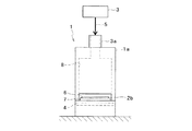
以下本発明の実施形態を図面に基づいて説明する。図1Aは正面視断面図、図1Bは右側面図を示している。
本発明の成膜方法を実施するに好適な本実施形態の成膜装置1は、成膜室2と、原料ガス供給手段3と、エネルギー供給手段4とを基本的に有する。前記成膜室2と前記エネルギー供給手段4は断熱性ボディ1a内に収容されている。
前記成膜室2は、キャリアガスと共に原料を基板面に沿って流動させる。前記成膜室2は、高さの低い前後左右に拡がる直方体空間を有している。例えば、前記成膜室2の大きさは、前後方向に約120mm、左右方向に約16mm、高さは約1.5mmである。
前記成膜室2は、原料ガス流入口2aとガス排出口2bを有する。前記原料ガス流入口2aは一端側、例えば左端側の上面に設けられた前後方向に延びる矩形の開口である。ガス排出口2bは他端側、例えば右側面に設けられた前後方向に延びる開口である。原料ガス流入口2aの開口面とガス排出口2bの開口面の向きは略90度異なっている。
Hereinafter, embodiments of the present invention will be described with reference to the drawings. 1A is a front sectional view, and FIG. 1B is a right side view.
A
The
The
原料ガス供給手段3は、膜を形成するための原料ガス5を前記成膜室2の原料ガス流入口2aへ所定の流速で供給する。原料ガス供給手段3としては、図4に示すような霧化装置が挙げられる。この場合、原料ガスは、原料がとかされた水溶液が霧化された原料水溶液及びそれを運ぶキャリアガスを含む。例えば、酢酸亜鉛水溶液が霧化されて窒素ガスによってキャリアされたものが挙げられる。 原料ガス供給手段3は、約1リットル/min以上約10リットル/min以下の範囲内の所定量の原料ガスを約0.4m/sec以上約4.0m/sec以下の範囲内の所定の速度で成膜室2内の前記基板6表面上に流すように、成膜室2の原料ガス流入口2aへ原料ガス5を供給する速度や、後述する予備加熱室8へ原料ガス5を供給する速度を調整する。
エネルギー供給手段4は、薄膜形成用のエネルギーを供給する手段である。エネルギー供給手段4として、ヒータやレーザー等が挙げられる。本実施形態においては、ヒータ4を例にとり説明する。
ヒータ4は、前記成膜室2の底に沿って前記成膜室2の全長に亘って設けられており、所定の温度まで、前記成膜室2、精確には前記基板6を加熱する。前記所定の温度とは、原料ガス5が成膜室2に流入したとき基板6上で化学的気相成膜反応を起こす温度である。
The source gas supply means 3 supplies a
The energy supply means 4 is means for supplying energy for forming a thin film. Examples of the energy supply means 4 include a heater and a laser. In the present embodiment, the heater 4 will be described as an example.
The heater 4 is provided over the entire length of the
基板6は、前記成膜室2内の原料ガス流入口2aとガス排出口2bとの間に配置される。基板6は、成膜室2内において直接成膜室2の底面と接触しないようにサセプタ7に載置されている。前記基板6としては、ガラス基板、石英基板、サファイア等が挙げられる。
The
前記基板6の一方の面、例えば上面だけに成膜する場合、前記サセプタ7は厚みの小さい、例えば、約0.5mm以上約2.0mm以下の範囲内の所定の厚みを有する一枚の平板であることが好ましい。前記基板6の他方の面、例えば下面側に原料ガスが殆ど回り込まないように、前記基板6の下面が、全面に渡って前記サセプタ7と密着するように載置する。そして、前記サセプタ7の下面側にも原料ガスが殆ど回り込まないように前記サセプタ7を成膜室2の底面に密着して配置する。
そして、前記基板6の成膜される側の表面(以下、成膜用表面という。)、例えば上面と成膜室2の内壁との距離Dが約0.1mm以上約10.0mm以下の範囲内の所定の距離となるように成膜室2の高さを定める。
When the film is formed only on one surface of the
Then, the distance D between the surface of the
前記基板6の両面に成膜する場合、前記サセプタ7は、記基板6の一方の面、例えば下面を部分的に支えるフレームであることが好ましい。基板6の両面からそれぞれ前記成膜室2の内壁との距離Dが約0.1mm以上約10.0mm以下の範囲内の所定の距離となるように成膜室2の高さやサセプタ7の厚みを定める。
When the film is formed on both surfaces of the
前記原料ガス供給手段3と前記成膜室2の原料ガス流入口2a間に、前記原料ガス5を予備加熱する予備加熱室8を設ける。前記予備加熱室8は、原料ガス流入口2aと連続するように成膜室2に隣接して前記断熱性ボディ1a内に設けることが好ましい。例えば、前記成膜室2の原料ガス流入口2aから立設するダクトのような形状をしている。例えば、前記予備加熱室8の大きさは、前後方向に約20mm、左右方向に約20mm、高さは約70mmである。
このような構造にすると、成膜室2の底に沿って設けられたヒータ4の予熱が予備加熱室8に伝わり、予備加熱室8用のヒータを別途設ける必要がない。尚、予備加熱室8用のヒータを設けてもよい。
A preheating
With such a structure, the preheating of the heater 4 provided along the bottom of the
予備加熱熱室8の上面において原料供給手段3の原料ガス供給路3aと接続されている。予備加熱温度は、原料ガス5が化学的気相成膜反応を起こさない範囲の温度である。成膜室2に移動したとき、始めて基板6上で原料ガス5が化学的気相成膜反応を起こすように調整する。
原料ガス5が、酢酸亜鉛水溶液が霧化されて窒素ガスによってキャリアされたものである場合、前記ヒータ4によって成膜室2内温度、精確には基板6温度を約280℃以上約430℃以下の範囲内の所定の温度に調整することが好ましい。この温度範囲に調整すると、基板6上に酸化亜鉛の透明な膜が生成される。
The upper surface of the preheating
In the case where the
上記構造の成膜装置を用いた成膜方法を説明する。
原料ガス供給手段3から原料ガス供給路3aを通じて、原料ガス5が予備加熱室8へ送り込まれる。予備加熱室8で滞留して所定の温度まで昇温される。前記所定の温度は、予備加熱室8において、原料ガス中の原料を分解させることのない温度、言い換えれば、化学的気相成膜反応が起こらないように、化学的気相成膜反応が起る温度よりも若干低めの温度である。
A film forming method using the film forming apparatus having the above structure will be described.
The
前記予備加熱された原料ガス5は、成膜室2に原料ガス流入口2aを通って流入する。
このとき、基板6は成膜室2内で所定の温度にまでヒータ4により昇温されている。
前記所定の温度とは、成膜室2内の基板6上で、原料ガス中の原料を分解する温度、言い換えれば、化学的気相成膜反応が起る温度である。
The
At this time, the
The predetermined temperature is a temperature at which the raw material in the raw material gas is decomposed on the
前記成膜室2に流入してきた原料ガス5は、前記基板6の成膜用表面に沿う方向に流れ、言い換えると、基板6の成膜用表面と略平行に流れ、基板表面上で原料ガス中の原料が分解して基板の成膜用表面に膜を生成する。所定量の原料ガスが基板6の成膜用表面上を流れるときの流速は約0.4m/sec以上約4.0m/sec以下の範囲の所定の高速度であることが好ましい。前記原料ガスの所定量は、約1リットル/min以上約10リットル/min以下の範囲にある所定量であることが好ましい。このような高速となるように、原料ガス供給手段3から予備加熱室8へ原料ガス5が送り込まれる速度や、予備加熱室8の大きさを適切に設定しておく。
そして、基板6上で化学的気相成膜反応を起こし、成膜を終えた残りのガスが成膜室2のガス排出口2bから排出される。
The
Then, a chemical vapor deposition reaction is caused on the
このように本発明の実施形態に係る成膜方法は、上記構造の成膜装置を用いて行うことができる。
従来のように、基板面に対して垂直方向に原料を流動させることにより基板面と原料とを接触させて膜を生成していた場合には、原料の分解物が基板面に接触している時間が比較的に短時間になるため、例えば分解物が基板面や分解物の膜に付着するのに要する付着時間が長い原料を用いて膜を生成することは困難である。
これに対し、本実施形態の成膜方法によれば、基板面に沿って原料をキャリアガスと共に流動させながら原料の分解を行って膜を生成するため、原料の分解物が膜に接触する時間を比較的に長時間確保することができる。これにより、例えば分解物が基板面や分解物の膜に付着するのに要する付着時間が長い原料を用いて膜を生成した場合であっても、膜を容易に生成することができる。
As described above, the film forming method according to the embodiment of the present invention can be performed using the film forming apparatus having the above structure.
In the case where a film is formed by bringing the substrate surface into contact with the raw material by flowing the raw material in a direction perpendicular to the substrate surface as in the prior art, the decomposition product of the raw material is in contact with the substrate surface. Since the time is relatively short, for example, it is difficult to form a film using a raw material having a long attachment time required for the decomposition product to adhere to the substrate surface or the decomposition product film.
On the other hand, according to the film forming method of this embodiment, since the raw material is decomposed while flowing the raw material along with the carrier gas along the substrate surface to generate a film, the time during which the decomposition product of the raw material contacts the film Can be secured for a relatively long time. Thereby, for example, even when a film is generated using a raw material having a long attachment time required for the decomposition product to adhere to the substrate surface or the decomposition product film, the film can be easily generated.
加えて、上記本実施形態に係る成膜方法及び成膜装置によると、前記基板6の成膜用表面と前記成膜室2の内壁との距離が約0.1mm以上約10.0mm以下の範囲の所定の距離と極狭小であるので、原料ガス5は成膜室2の内壁によって基板の成膜用表面に押し付けられたと同様な状態になり、基板6の成膜用表面を流れる原料ガス5はショートパスすることなく基板6の成膜用表面上で反応して成膜する。
更に、原料ガス5の速度が、約0.4m/sec以上約4.0m/sec以下の範囲の所定の高速度であるので、原料ガス5は基板の成膜用表面上で乱流となり、基板の成膜表面と良く接触する。そのため、原料ガスはショートパスすることなく基板の成膜用表面上で反応して成膜する。
In addition, according to the film forming method and film forming apparatus of the present embodiment, the distance between the film forming surface of the
Furthermore, since the speed of the
また、膜の成長速度が、成膜室2内のどの位置にあるかによって異なる場合がある。
図2は、成膜室2の原料ガス流入口2a側の所定の基準位置Sからの距離と膜の成長速度との関係を示すグラフである。原料ガス流入口2aから遠ざかるにつれて成長速度が低下していることが判る。
Further, the film growth rate may vary depending on the position in the
FIG. 2 is a graph showing the relationship between the distance from the predetermined reference position S on the
この場合、膜の厚みを均一にするために、前記基板面が存在する範囲おける前記原料の流路面積を、上流側よりも下流側の方が減少した状態にするとよい。
具体的には、前記基板6の成膜用表面と前記成膜室2の内壁との距離Dを原料ガス5が流れる向きfに沿って上流側から下流側へと狭くなるように、前記成膜室2の高さを原料ガス流入口2aからガス排出口2bへ向かうにつれ低くするとよい。
上記の構成によれば、流路面積が減少されることによって、基板面周辺の圧力が高まり、原料の分解が促進されると共に、基板面への分解物の付着が促進される。これにより、効率良く基板面に膜を生成することができる。
In this case, in order to make the thickness of the film uniform, the flow area of the raw material in the range where the substrate surface exists is preferably reduced in the downstream side than in the upstream side.
More specifically, the distance D between the film forming surface of the
According to the above configuration, by reducing the flow channel area, the pressure around the substrate surface is increased, the decomposition of the raw material is promoted, and the attachment of the decomposed material to the substrate surface is promoted. Thereby, a film can be efficiently generated on the substrate surface.
また、膜の厚みを均一にするために、前記原料の流動方向に対して前記基板面を進退移動させる、言い換えれば、前記成膜室2の原料ガス流入口2aと前記基板6とを相対移動させることが好ましい。
上記の構成によれば、原料の分解の状態や基板面に対する分解物の付着の状態が流動方向において不均一であった場合でも、基板面を流動方向に対して進退移動させることによって、基板面に対する付着の程度を平均化し、均一な膜を基板面全体に生成することができる。
Further, in order to make the film thickness uniform, the substrate surface is moved back and forth with respect to the flow direction of the raw material, in other words, the raw
According to the above configuration, even when the state of decomposition of the raw material and the state of decomposition product adhesion to the substrate surface are non-uniform in the flow direction, the substrate surface is moved forward and backward in the flow direction. It is possible to average the degree of adhesion to the substrate and to form a uniform film over the entire substrate surface.
具体的には、図3に示すようように、前記基板6を前記成膜室2の少なくとも原料ガス流入口2aとガス排出口2bとの間で搬送する手段9を更に有して前記基板6を少なくとも原料ガスの流れる向きfに逆らって搬送することが好ましい。
図3において、搬送手段9としては、サセプタを兼ねるベルトコンベア、若しくは、基板6を載置したサセプタ7を搬送するベルトコンベア等が挙げられる。前記搬送手段9は前記成膜室2のガス排出口2b側から原料ガス流入口2a付近に渡る長さを有して成膜室2内の底に設置されている。成膜中は、原料ガスの流れる向きfとは反対の向きmに基板6を搬送する。成膜後は、成膜室2のガス排出口2bから排出する方向に基板6を搬送する。尚、成膜中に基板を搬送する方向は前記原料ガスの流れる向きfとは反対の向きmに限らず、膜の厚みを均一にするために、適宜向きを変えて搬送してもよい。
Specifically, as shown in FIG. 3, the
In FIG. 3, examples of the conveying
更にまた、膜の厚みを均一にするために、前記成膜室2の原料ガス流入口2aを前記基板6に対して移動させる手段を設けて、前記成膜室2の原料ガス流入口2aを少なくとも原料ガスの流れる向きfと同じ向きに移動させてもよい。
Furthermore, in order to make the film thickness uniform, a means for moving the
次に、図4を参照しつつ材料ガス供給手段3の一例である霧化装置3について説明する。
図4において、31は第1容器、32は第2容器、33は伝搬溶液、34は原料水溶液、35は第2容器の底部材、36は超音波振動子、37はキャリアガス供給装置、38キャリアガス流量制御弁を示している。
第1容器31内に伝搬溶液33が収容されている。第2溶液32に原料が溶かされた原料水溶液34が収容されている。伝搬溶液33の液面が原料水溶液34の液面よりも高くなる程度まで前記第2容器32の底部材35が前記伝搬溶液33内に浸漬されている。前記第2容器32の上部側面にキャリアガス導入口32aが、上面に原料ガス供給路3aと接続されるガス排出口32bが設けられている。キャリアガス供給装置37がキャリアガス流量制御弁38を介して前記第2容器32のキャリアガス導入口32aに接続されている。
Next, the
In FIG. 4, 31 is a first container, 32 is a second container, 33 is a propagation solution, 34 is a raw material aqueous solution, 35 is a bottom member of the second container, 36 is an ultrasonic vibrator, 37 is a carrier gas supply device, 38 A carrier gas flow control valve is shown.
A propagation solution 33 is accommodated in the
第1容器31及び第2容器32としてガラス製容器が挙げられる。第2容器の底部材35としては、高分子フィルムが挙げられる。伝搬溶液33としてエタノールが挙げられる。原料水溶液34としては、酢酸亜鉛水溶液が挙げられる。キャリアガス供給装置37としては、窒素ガスボンベが挙げられる。
上記構造の霧化装置3の作動を説明する。第1容器31の底に配置された超音波振動子36が作動する。超音波は、第1容器31内の伝搬溶液33を伝播し、第2容器32の底面部材35を透過して原料水溶液34に伝播する。この結果、原料水溶液34は、超音波により振動され、液体同士の結合が外れることにより霧状となって放出される。これが霧化された原料水溶液(ミスト)である。
Examples of the
The operation of the
上記のようにして霧化された原料水溶液が生成されると、この生成タイミングに一致したタイミングや僅かに前後したタイミングで流量制御弁38が開栓される。そして、キャリアガス供給装置37のキャリアガスが流量制御弁38の開度に応じた供給量で第2容器32内に供給される。これにより、霧化された原料水溶液は、キャリアガスと共に第2容器32から原料ガス供給路3aへ排出され、原料供給路3a介して成膜装置1に供給される。この霧化された原料水溶液及びそれを運ぶキャリアガスを含むガスが成膜装置1の原料ガス5となる。前記キャリアガスによる霧化された原料水溶液の原料ガス供給路3aへの排出速度を調整することにより、成膜装置1への原料ガス5の供給速度を制御する。
When the atomized raw material aqueous solution is generated as described above, the
図1 Aに示した成膜装置において、超音波で噴霧した0.05M酢酸亜鉛水溶液を3L/minの窒素ガスによってキャリアさせた原料ガス5を原料ガス供給手段3から成膜室2に供給した。基板温度280℃以上430℃以下の範囲の所定の温度において成膜を行った。用いた基板の大きさは、縦約15mm、横約15mm、高さ約0.7mmであった。
その結果、綴密な透明なZnOの薄膜が得られた。前記生成された膜の大きさは、縦約15mm、横約15mm、厚み約0.2μm(200nm)であった。
また、成膜室2のガス排出口2bから排出されるガス中には、酢酸亜鉛の成分が殆どなく原料を効率よく利用できた。更に、原料ガス成分として酢酸亜鉛水溶液を用いているので比較的高額な酸素ガスを用いる必要がなく、キャリアガスとして窒素を採用することができた。
In the film forming apparatus shown in FIG. 1A, a
As a result, a tight transparent ZnO thin film was obtained. The size of the generated film was about 15 mm in length, about 15 mm in width, and about 0.2 μm (200 nm) in thickness.
Further, the gas discharged from the
前記非特許文献1に記載のような成膜装置を用いて、超音波で噴霧した0.05M酢酸亜鉛水溶液を3L/minの窒素ガスによって成膜室2に輸送させ、基板温度280℃以上430℃以下の範囲の所定の温度において成膜を行った。基板としては、縦約15mm、横約15mm、高さ約0.7mmまでの大きさの基板しか使用できなかった。
その結果、あまり緻密でないムラのある膜ができた。前記生成された膜の大きさは、縦約15mm、横約10mm、厚み約3μm(3000nm)であった。
Using a film forming apparatus as described in
As a result, a non-dense and uneven film was obtained. The size of the produced film was about 15 mm in length, about 10 mm in width, and about 3 μm (3000 nm) in thickness.
図3に示した成膜装置おいて、2.4MHz・12Wの超音波振動子を用いて霧化させた0.05M酢酸亜鉛水溶液を3.0L/minの窒素ガスによってキャリアさせた原料ガス5を原料ガス供給手段3から成膜室2に供給した。一方、4mm/minの速さで基板6を前記原料ガス5の流れる向きfと逆向きmに動かした。この結果、10分で厚さ200nmの均一な膜ができた。
In the film forming apparatus shown in FIG. 3, a
このように、本実施形態に係る成膜方法及び成膜装置を使用することにより、原料を効率よく利用できるので、より高純度な綴密な薄膜を安価に生成することができる。そして、成膜する表面が比較的広く、効率良く、安価に成膜することのできる。加えて、成膜室を真空等にする必要もないので安価である。
また、原料を強制的に付着させることができるのであらゆる成膜法に有効であると思われる。すなわち産業にとって極めて有用である。
As described above, since the raw material can be efficiently used by using the film forming method and the film forming apparatus according to the present embodiment, a higher-purity, dense thin film can be generated at low cost. In addition, the film can be formed on a relatively wide surface, efficiently, and inexpensively. In addition, the film forming chamber does not need to be evacuated, so that it is inexpensive.
Further, since the raw material can be forcibly adhered, it is considered to be effective for all film forming methods. That is, it is extremely useful for industry.
尚、上記実施形態では、成膜室2の原料ガス流入口2aの開口面と原料ガス排出口2bの開口面が約90度異なり、そのため予備加熱室8が成膜室2の上面側に立設した構造となっている。しかしながら、成膜室2の原料ガス流入口2aの開口面を左側面側に位置するようにして、成膜室2と予備加熱室8とが左右方向に一列に並ぶ構造とすることもできる。 その場合も、前記基板6の成膜用表面と成膜室2の内壁との距離を約0.1mm以上約10.0mm以下の範囲内の所定の距離とし、約0.4m/sec以上約4.0m/sec以下の範囲内の所定の速度で原料ガス5を前記基板6の成膜用表面に沿うように流すことが肝要である。
また、本発明は、上記の好ましい実施形態に記載されているが、本発明はそれだけに制限されない。本発明の精神と範囲から逸脱することのない様々な実施形態例が他になされることができることは理解されよう。
In the above embodiment, the opening surface of the
Moreover, although this invention is described in said preferable embodiment, this invention is not restrict | limited only to it. It will be understood that various other exemplary embodiments may be made without departing from the spirit and scope of the invention.
1 成膜装置
1a 断熱性ボディ
2 成膜室
2a 原料ガス流入口
2b 原料ガス排出口
3 原料ガス供給手段
3a 原料ガス供給路
4 ヒータ
5 原料ガス
6 基板
7 サセプタ
8 予備加熱室
9 ベルトコンベア
D 距離
f 原料ガスの流れる向き
1 Deposition system
1a Thermal insulation body
2 Deposition chamber
2a Raw material gas inlet
2b Raw material gas outlet
3 Raw material gas supply means
3a Raw material gas supply path
4 Heater
5
Claims (4)
前記基板の表面と前記成膜室における上側の内壁との距離を0.1mm以上10.0mm以下の範囲内の所定の距離とし、
前記原料ガス供給手段から供給される霧化された原料水溶液及びそれを運ぶキャリアガスを含む前記原料ガスを、当該原料ガス供給手段と前記成膜室との間の予備加熱室で滞留させて予備加熱し、
その後、0.4m/sec以上4.0m/sec以下の範囲内の所定の速度で、前記基板表面上に前記原料ガスを流す化学的気相成膜方法。 A chemical vapor deposition method for forming a film on the surface of a substrate by placing the substrate in a rectangular parallelepiped-shaped film formation chamber and causing the source gas supplied from the source gas supply means to flow in a direction along the substrate surface. Because
The distance between the surface of the substrate and the upper inner wall in the film forming chamber is a predetermined distance within a range of 0.1 mm to 10.0 mm,
The raw material gas containing the atomized raw material aqueous solution supplied from the raw material gas supply means and the carrier gas carrying the raw material gas is retained in a preheating chamber between the raw material gas supply means and the film forming chamber, and is reserved. Heated,
Thereafter, a chemical vapor deposition method in which the source gas is allowed to flow on the substrate surface at a predetermined speed within a range of 0.4 m / sec to 4.0 m / sec.
霧化された原料水溶液及びそれを運ぶキャリアガスを含む原料ガスを供給する原料ガス供給手段と、
薄膜形成用のエネルギーを供給するエネルギー供給手段と、
前記原料ガス供給手段と前記成膜室の前記原料ガス流入口との間に設けられた、前記エネルギー供給手段によって前記原料ガスを予備加熱する予備加熱室と、
を備え、
前記基板表面に沿う方向に前記原料ガスを流動させることにより前記基板の表面に膜を生成する化学的気相成膜装置であって、
前記基板表面と前記成膜室における上側の内壁との距離が0.1mm以上10.0mm以下の範囲の所定の距離であり、前記原料ガス供給手段から供給される前記原料ガスが、前記予備加熱室で滞留して予備加熱され、その後、0.4m/sec以上4.0m/sec以下の範囲内の所定の速度で前記基板表面上に流されることを特徴とする成膜装置。 A rectangular parallelepiped-shaped film formation chamber having a source gas inlet and a gas outlet, and a substrate is disposed between the source gas inlet and the gas outlet,
A raw material gas supply means for supplying a raw material gas including an atomized raw material aqueous solution and a carrier gas carrying the same,
Energy supply means for supplying energy for thin film formation;
A preheating chamber provided between the source gas supply means and the source gas inlet of the film formation chamber for preheating the source gas by the energy supply means;
With
A chemical vapor deposition apparatus that generates a film on the surface of the substrate by flowing the source gas in a direction along the surface of the substrate,
The distance between the substrate surface and the upper inner wall in the film forming chamber is a predetermined distance in the range of 0.1 mm to 10.0 mm, and the source gas supplied from the source gas supply means A film forming apparatus characterized in that the film stays in the chamber and is preheated, and then is flowed over the substrate surface at a predetermined speed within a range of 0.4 m / sec to 4.0 m / sec.
Priority Applications (1)
| Application Number | Priority Date | Filing Date | Title |
|---|---|---|---|
| JP2004122834A JP5124760B2 (en) | 2004-04-19 | 2004-04-19 | Film forming method and film forming apparatus |
Applications Claiming Priority (1)
| Application Number | Priority Date | Filing Date | Title |
|---|---|---|---|
| JP2004122834A JP5124760B2 (en) | 2004-04-19 | 2004-04-19 | Film forming method and film forming apparatus |
Publications (2)
| Publication Number | Publication Date |
|---|---|
| JP2005307238A JP2005307238A (en) | 2005-11-04 |
| JP5124760B2 true JP5124760B2 (en) | 2013-01-23 |
Family
ID=35436338
Family Applications (1)
| Application Number | Title | Priority Date | Filing Date |
|---|---|---|---|
| JP2004122834A Expired - Fee Related JP5124760B2 (en) | 2004-04-19 | 2004-04-19 | Film forming method and film forming apparatus |
Country Status (1)
| Country | Link |
|---|---|
| JP (1) | JP5124760B2 (en) |
Families Citing this family (26)
| Publication number | Priority date | Publication date | Assignee | Title |
|---|---|---|---|---|
| JP4704894B2 (en) * | 2005-11-16 | 2011-06-22 | 国立大学法人京都大学 | Film forming method and film forming apparatus |
| JP2007254821A (en) * | 2006-03-23 | 2007-10-04 | Kaneka Corp | Method for producing substrate provided with transparent electroconductive film, and apparatus therefor |
| CN104488071B (en) * | 2012-05-24 | 2017-10-13 | 株式会社尼康 | Substrate board treatment and device making method |
| JP6137668B2 (en) * | 2012-08-26 | 2017-05-31 | 国立大学法人 熊本大学 | Zinc oxide crystal layer manufacturing method and mist chemical vapor deposition apparatus |
| JP5343162B1 (en) * | 2012-10-26 | 2013-11-13 | エピクルー株式会社 | Epitaxial growth equipment |
| KR101764987B1 (en) * | 2012-11-05 | 2017-08-03 | 도시바 미쓰비시덴키 산교시스템 가부시키가이샤 | Film-forming apparatus |
| JP6103633B2 (en) * | 2013-02-08 | 2017-03-29 | 高知県公立大学法人 | Ozone-supported high-quality homogeneous metal oxide thin film fabrication technology, and oxide thin-film transistor manufacturing method using the thin-film fabrication technology |
| JP6478103B2 (en) | 2015-01-29 | 2019-03-06 | 株式会社Flosfia | Film forming apparatus and film forming method |
| EP3051002A1 (en) | 2015-01-29 | 2016-08-03 | Flosfia Inc. | Apparatus and method for forming film |
| JP6778869B2 (en) * | 2015-12-11 | 2020-11-04 | 株式会社Flosfia | Method for manufacturing silicon oxide film |
| JP6721936B2 (en) * | 2016-02-18 | 2020-07-15 | 株式会社桧鉄工所 | Atomizer |
| JP6721937B2 (en) * | 2016-02-18 | 2020-07-15 | 株式会社桧鉄工所 | Atomizer |
| JP6980180B2 (en) * | 2016-11-10 | 2021-12-15 | 株式会社Flosfia | Film forming equipment and film forming method |
| JP6749295B2 (en) * | 2017-08-22 | 2020-09-02 | アプライド マテリアルズ インコーポレイテッドApplied Materials,Incorporated | Film forming method by epitaxial growth and epitaxial growth apparatus |
| JP6875336B2 (en) | 2018-08-27 | 2021-05-26 | 信越化学工業株式会社 | Film formation method |
| JP6934852B2 (en) | 2018-12-18 | 2021-09-15 | 信越化学工業株式会社 | Manufacturing method of gallium oxide film |
| KR20220166283A (en) | 2020-04-13 | 2022-12-16 | 신에쓰 가가꾸 고교 가부시끼가이샤 | Film formation device and film formation method |
| JP6925548B1 (en) | 2020-07-08 | 2021-08-25 | 信越化学工業株式会社 | Manufacturing method and film forming equipment for gallium oxide semiconductor film |
| EP4202077A4 (en) | 2020-08-20 | 2024-08-21 | Shinetsu Chemical Co | Film formation method and raw material solution |
| CN114182235B (en) * | 2020-09-14 | 2023-09-29 | 北京环境特性研究所 | Method for establishing gas balance flow field in growth chamber |
| TWM634737U (en) | 2021-03-12 | 2022-12-01 | 日商信越化學工業股份有限公司 | Gallium-based oxide semiconductor film, and film-forming system and semiconductor device thereof |
| TWM636275U (en) | 2021-03-12 | 2023-01-11 | 日商信越化學工業股份有限公司 | Film forming system and film forming apparatus |
| CN217781272U (en) | 2021-05-04 | 2022-11-11 | 信越化学工业株式会社 | Film forming system |
| KR20240074787A (en) | 2021-10-14 | 2024-05-28 | 신에쓰 가가꾸 고교 가부시끼가이샤 | Film formation device and manufacturing method |
| KR20240101567A (en) | 2021-11-02 | 2024-07-02 | 신에쓰 가가꾸 고교 가부시끼가이샤 | Film formation equipment and film formation method, oxide semiconductor film and laminate |
| WO2023149037A1 (en) * | 2022-02-04 | 2023-08-10 | 株式会社村田製作所 | Mist cvd film forming device and film forming method |
Family Cites Families (8)
| Publication number | Priority date | Publication date | Assignee | Title |
|---|---|---|---|---|
| JPS4942423B1 (en) * | 1970-12-22 | 1974-11-14 | ||
| JPS63233521A (en) * | 1987-03-23 | 1988-09-29 | Nissan Motor Co Ltd | Vapor phase reaction tube |
| JP2881828B2 (en) * | 1989-08-04 | 1999-04-12 | 富士通株式会社 | Vapor phase growth apparatus and vapor phase growth method |
| FR2672519B1 (en) * | 1991-02-13 | 1995-04-28 | Saint Gobain Vitrage Int | NOZZLE WITH HEAVY DOWNSTREAM HEEL, FOR DEPOSITING A COATING LAYER ON A TAPE OF GLASS, BY PYROLYSIS OF A GASEOUS MIXTURE. |
| JP3149468B2 (en) * | 1991-09-03 | 2001-03-26 | 株式会社日立製作所 | CVD equipment |
| JP3338884B2 (en) * | 1993-09-20 | 2002-10-28 | 株式会社日立製作所 | Semiconductor processing equipment |
| JP3042335B2 (en) * | 1994-10-25 | 2000-05-15 | 信越半導体株式会社 | Vapor phase growth method and apparatus |
| JP3545498B2 (en) * | 1995-06-27 | 2004-07-21 | 株式会社ルネサステクノロジ | Method for manufacturing semiconductor device |
-
2004
- 2004-04-19 JP JP2004122834A patent/JP5124760B2/en not_active Expired - Fee Related
Also Published As
| Publication number | Publication date |
|---|---|
| JP2005307238A (en) | 2005-11-04 |
Similar Documents
| Publication | Publication Date | Title |
|---|---|---|
| JP5124760B2 (en) | Film forming method and film forming apparatus | |
| TW466587B (en) | Apparatus for deposition of thin films on wafers through atomic layer epitaxial process | |
| JP2001137800A5 (en) | ||
| CN101939827B (en) | Liquid material carburetor, and filming device using the carburetor | |
| US20130220221A1 (en) | Method and apparatus for precursor delivery | |
| WO1993013244A1 (en) | Surface reaction film formation apparatus | |
| JP7357301B2 (en) | Semiconductor film and method for manufacturing semiconductor film | |
| KR20100037071A (en) | Heating element cvd apparatus | |
| WO2021172154A1 (en) | Film-forming atomization device and film-forming device using same | |
| JP4708130B2 (en) | Film forming apparatus and method for producing transparent conductive film | |
| JP7358714B2 (en) | Film-forming equipment and film-forming method | |
| US20090205570A1 (en) | Gas supply unit and chemical vapor deposition apparatus | |
| JP3179864B2 (en) | Thin film forming equipment | |
| JP4991950B1 (en) | Mist deposition system | |
| WO2012049922A1 (en) | Film-forming apparatus and film-forming method | |
| JP2000087852A (en) | Vacuum device with reaction product removing function and reaction product removing method thereof | |
| JP2664886B2 (en) | Silicon film forming method and silicon film forming apparatus | |
| JP2005327995A (en) | Catalyst cvd equipment | |
| JP3644864B2 (en) | Deposition equipment | |
| RU2188878C2 (en) | Method of application of amorphous silicon films and device for realization of this method | |
| JP2721222B2 (en) | Source gas supply device for plasma CVD | |
| WO2024185380A1 (en) | Film formation nozzle and film formation device | |
| JP5114457B2 (en) | Catalytic CVD equipment | |
| JP2007173747A (en) | Cvd apparatus and cleaning method | |
| JP2010245478A (en) | Plasma processing apparatus |
Legal Events
| Date | Code | Title | Description |
|---|---|---|---|
| A621 | Written request for application examination |
Free format text: JAPANESE INTERMEDIATE CODE: A621 Effective date: 20070328 |
|
| A977 | Report on retrieval |
Free format text: JAPANESE INTERMEDIATE CODE: A971007 Effective date: 20090626 |
|
| A711 | Notification of change in applicant |
Free format text: JAPANESE INTERMEDIATE CODE: A711 Effective date: 20090901 |
|
| A521 | Request for written amendment filed |
Free format text: JAPANESE INTERMEDIATE CODE: A821 Effective date: 20090903 |
|
| A521 | Request for written amendment filed |
Free format text: JAPANESE INTERMEDIATE CODE: A821 Effective date: 20090911 |
|
| A711 | Notification of change in applicant |
Free format text: JAPANESE INTERMEDIATE CODE: A711 Effective date: 20090911 |
|
| A521 | Request for written amendment filed |
Free format text: JAPANESE INTERMEDIATE CODE: A821 Effective date: 20090901 |
|
| A521 | Request for written amendment filed |
Free format text: JAPANESE INTERMEDIATE CODE: A821 Effective date: 20090911 |
|
| A521 | Request for written amendment filed |
Free format text: JAPANESE INTERMEDIATE CODE: A821 Effective date: 20091028 |
|
| A711 | Notification of change in applicant |
Free format text: JAPANESE INTERMEDIATE CODE: A711 Effective date: 20091028 |
|
| A521 | Request for written amendment filed |
Free format text: JAPANESE INTERMEDIATE CODE: A821 Effective date: 20091028 |
|
| A131 | Notification of reasons for refusal |
Free format text: JAPANESE INTERMEDIATE CODE: A131 Effective date: 20100622 |
|
| A521 | Request for written amendment filed |
Free format text: JAPANESE INTERMEDIATE CODE: A523 Effective date: 20100820 |
|
| A131 | Notification of reasons for refusal |
Free format text: JAPANESE INTERMEDIATE CODE: A131 Effective date: 20110111 |
|
| A521 | Request for written amendment filed |
Free format text: JAPANESE INTERMEDIATE CODE: A523 Effective date: 20110308 |
|
| A02 | Decision of refusal |
Free format text: JAPANESE INTERMEDIATE CODE: A02 Effective date: 20110628 |
|
| A521 | Request for written amendment filed |
Free format text: JAPANESE INTERMEDIATE CODE: A523 Effective date: 20110928 |
|
| A911 | Transfer to examiner for re-examination before appeal (zenchi) |
Free format text: JAPANESE INTERMEDIATE CODE: A911 Effective date: 20111006 |
|
| A912 | Re-examination (zenchi) completed and case transferred to appeal board |
Free format text: JAPANESE INTERMEDIATE CODE: A912 Effective date: 20120302 |
|
| A521 | Request for written amendment filed |
Free format text: JAPANESE INTERMEDIATE CODE: A523 Effective date: 20120808 |
|
| A01 | Written decision to grant a patent or to grant a registration (utility model) |
Free format text: JAPANESE INTERMEDIATE CODE: A01 |
|
| RD03 | Notification of appointment of power of attorney |
Free format text: JAPANESE INTERMEDIATE CODE: A7423 Effective date: 20120927 |
|
| A521 | Request for written amendment filed |
Free format text: JAPANESE INTERMEDIATE CODE: A821 Effective date: 20121010 |
|
| RD04 | Notification of resignation of power of attorney |
Free format text: JAPANESE INTERMEDIATE CODE: A7424 Effective date: 20121010 |
|
| A61 | First payment of annual fees (during grant procedure) |
Free format text: JAPANESE INTERMEDIATE CODE: A61 Effective date: 20121004 |
|
| R150 | Certificate of patent or registration of utility model |
Free format text: JAPANESE INTERMEDIATE CODE: R150 Ref document number: 5124760 Country of ref document: JP Free format text: JAPANESE INTERMEDIATE CODE: R150 |
|
| FPAY | Renewal fee payment (event date is renewal date of database) |
Free format text: PAYMENT UNTIL: 20151109 Year of fee payment: 3 |
|
| FPAY | Renewal fee payment (event date is renewal date of database) |
Free format text: PAYMENT UNTIL: 20151109 Year of fee payment: 3 |
|
| FPAY | Renewal fee payment (event date is renewal date of database) |
Free format text: PAYMENT UNTIL: 20151109 Year of fee payment: 3 |
|
| A521 | Request for written amendment filed |
Free format text: JAPANESE INTERMEDIATE CODE: A523 Effective date: 20130205 |
|
| R250 | Receipt of annual fees |
Free format text: JAPANESE INTERMEDIATE CODE: R250 |
|
| R250 | Receipt of annual fees |
Free format text: JAPANESE INTERMEDIATE CODE: R250 |
|
| LAPS | Cancellation because of no payment of annual fees |