JP5123185B2 - Through-hole plating method for semiconductor wafer - Google Patents
Through-hole plating method for semiconductor wafer Download PDFInfo
- Publication number
- JP5123185B2 JP5123185B2 JP2008528445A JP2008528445A JP5123185B2 JP 5123185 B2 JP5123185 B2 JP 5123185B2 JP 2008528445 A JP2008528445 A JP 2008528445A JP 2008528445 A JP2008528445 A JP 2008528445A JP 5123185 B2 JP5123185 B2 JP 5123185B2
- Authority
- JP
- Japan
- Prior art keywords
- laser
- wafer
- semiconductor wafer
- hole
- Prior art date
- Legal status (The legal status is an assumption and is not a legal conclusion. Google has not performed a legal analysis and makes no representation as to the accuracy of the status listed.)
- Expired - Fee Related
Links
Images


Classifications
-
- H—ELECTRICITY
- H01—ELECTRIC ELEMENTS
- H01L—SEMICONDUCTOR DEVICES NOT COVERED BY CLASS H10
- H01L21/00—Processes or apparatus adapted for the manufacture or treatment of semiconductor or solid state devices or of parts thereof
- H01L21/70—Manufacture or treatment of devices consisting of a plurality of solid state components formed in or on a common substrate or of parts thereof; Manufacture of integrated circuit devices or of parts thereof
- H01L21/71—Manufacture of specific parts of devices defined in group H01L21/70
- H01L21/768—Applying interconnections to be used for carrying current between separate components within a device comprising conductors and dielectrics
- H01L21/76898—Applying interconnections to be used for carrying current between separate components within a device comprising conductors and dielectrics formed through a semiconductor substrate
-
- H—ELECTRICITY
- H01—ELECTRIC ELEMENTS
- H01L—SEMICONDUCTOR DEVICES NOT COVERED BY CLASS H10
- H01L21/00—Processes or apparatus adapted for the manufacture or treatment of semiconductor or solid state devices or of parts thereof
- H01L21/02—Manufacture or treatment of semiconductor devices or of parts thereof
- H01L21/02041—Cleaning
- H01L21/02057—Cleaning during device manufacture
-
- H—ELECTRICITY
- H01—ELECTRIC ELEMENTS
- H01L—SEMICONDUCTOR DEVICES NOT COVERED BY CLASS H10
- H01L21/00—Processes or apparatus adapted for the manufacture or treatment of semiconductor or solid state devices or of parts thereof
- H01L21/02—Manufacture or treatment of semiconductor devices or of parts thereof
- H01L21/04—Manufacture or treatment of semiconductor devices or of parts thereof the devices having at least one potential-jump barrier or surface barrier, e.g. PN junction, depletion layer or carrier concentration layer
- H01L21/18—Manufacture or treatment of semiconductor devices or of parts thereof the devices having at least one potential-jump barrier or surface barrier, e.g. PN junction, depletion layer or carrier concentration layer the devices having semiconductor bodies comprising elements of Group IV of the Periodic System or AIIIBV compounds with or without impurities, e.g. doping materials
- H01L21/30—Treatment of semiconductor bodies using processes or apparatus not provided for in groups H01L21/20 - H01L21/26
- H01L21/302—Treatment of semiconductor bodies using processes or apparatus not provided for in groups H01L21/20 - H01L21/26 to change their surface-physical characteristics or shape, e.g. etching, polishing, cutting
- H01L21/306—Chemical or electrical treatment, e.g. electrolytic etching
- H01L21/30604—Chemical etching
- H01L21/30612—Etching of AIIIBV compounds
- H01L21/30621—Vapour phase etching
-
- H—ELECTRICITY
- H01—ELECTRIC ELEMENTS
- H01L—SEMICONDUCTOR DEVICES NOT COVERED BY CLASS H10
- H01L21/00—Processes or apparatus adapted for the manufacture or treatment of semiconductor or solid state devices or of parts thereof
- H01L21/02—Manufacture or treatment of semiconductor devices or of parts thereof
- H01L21/04—Manufacture or treatment of semiconductor devices or of parts thereof the devices having at least one potential-jump barrier or surface barrier, e.g. PN junction, depletion layer or carrier concentration layer
- H01L21/18—Manufacture or treatment of semiconductor devices or of parts thereof the devices having at least one potential-jump barrier or surface barrier, e.g. PN junction, depletion layer or carrier concentration layer the devices having semiconductor bodies comprising elements of Group IV of the Periodic System or AIIIBV compounds with or without impurities, e.g. doping materials
- H01L21/30—Treatment of semiconductor bodies using processes or apparatus not provided for in groups H01L21/20 - H01L21/26
- H01L21/302—Treatment of semiconductor bodies using processes or apparatus not provided for in groups H01L21/20 - H01L21/26 to change their surface-physical characteristics or shape, e.g. etching, polishing, cutting
- H01L21/306—Chemical or electrical treatment, e.g. electrolytic etching
- H01L21/3065—Plasma etching; Reactive-ion etching
-
- H—ELECTRICITY
- H01—ELECTRIC ELEMENTS
- H01L—SEMICONDUCTOR DEVICES NOT COVERED BY CLASS H10
- H01L2924/00—Indexing scheme for arrangements or methods for connecting or disconnecting semiconductor or solid-state bodies as covered by H01L24/00
- H01L2924/0001—Technical content checked by a classifier
- H01L2924/0002—Not covered by any one of groups H01L24/00, H01L24/00 and H01L2224/00
Landscapes
- Engineering & Computer Science (AREA)
- Physics & Mathematics (AREA)
- Power Engineering (AREA)
- Condensed Matter Physics & Semiconductors (AREA)
- General Physics & Mathematics (AREA)
- Manufacturing & Machinery (AREA)
- Computer Hardware Design (AREA)
- Microelectronics & Electronic Packaging (AREA)
- Chemical & Material Sciences (AREA)
- Plasma & Fusion (AREA)
- Chemical Kinetics & Catalysis (AREA)
- General Chemical & Material Sciences (AREA)
- Internal Circuitry In Semiconductor Integrated Circuit Devices (AREA)
- Drying Of Semiconductors (AREA)
- Laser Beam Processing (AREA)
- Weting (AREA)
- Junction Field-Effect Transistors (AREA)
Description
本発明は、半導体デバイスの製作のための半導体ウエハ内の垂直貫通めっきホール(マイクロ・ビア、ポケット・ホール・ビアまたは「ブラインド」ビア、ビア=垂直の相互接続通路)、すなわち、ウエハの前側から半導体ウエハを貫通してウエハの後側まで延びるコンタクトの形成方法に関する。 The present invention relates to vertical through-plated holes (micro vias, pocket hole vias or “blind” vias, vias = vertical interconnect paths) in a semiconductor wafer for the fabrication of semiconductor devices, ie from the front side of the wafer. The present invention relates to a method of forming a contact that extends through a semiconductor wafer to the rear side of the wafer.
デバイスの特性(例えば、高周波特性)は、周辺部にさらに小さく集積化することによってのみ、十分に活用することができる。短い垂直接続は電気的コンタクトの効果的な方法を表す。さらに、チップ当たりの利用できる高周波トランジスタの増幅率および最大出力を増強するためという物理的理由のために、前側上のソース・コンタクトと後側上の接地電極との間に低インダクタンスの導電性接続を構築する必要がある。しかしながら、これは、その技術を考えると必ずしも容易に実施することができない。 Device characteristics (for example, high-frequency characteristics) can be fully utilized only by further integration in the periphery. A short vertical connection represents an effective method of electrical contact. In addition, a low inductance conductive connection between the source contact on the front side and the ground electrode on the rear side for physical reasons to increase the gain and maximum power of the available high frequency transistors per chip. Need to build. However, this cannot always be easily implemented given the technology.
電気的に活性なGaN(窒化ガリウム)材料は、現在のところ実質的には単結晶ウエハ材料としては利用できず、したがって、例えばSiC(炭化シリコン)ウエハなどの基板材料上にエピタキシャル成長させている。 Electrically active GaN (gallium nitride) materials are currently not practically available as single crystal wafer materials and are therefore epitaxially grown on substrate materials such as, for example, SiC (silicon carbide) wafers.
SiCは、その非常に高い化学的安定性および大きな硬度と同様に、その非常に良好な熱伝導性もよく知られている。したがって、GaNトランジスタの後側にコンタクトするためには、重ねられたエピタキシャルGaN層を貫通するのと同様に、SiCのキャリア材料も貫通して穴開けをする必要がある。テクスチャ化のためには、今まで、この目的のために特別に最適化された高性能プラズマ・エッチング反応装置での、反応性イオン・エッチング等の乾式化学エッチング処理のみが実際には使用可能であった。しかしながら、SiCの典型的なプラズマ・エッチング速度は1μm/minと非常に低い。さらに、プラズマ・エッチング技術の使用には、耐久性のあるエッチング・マスクの製作およびリソグラフィによるテクスチャ化が必要である。 SiC is well known for its very good thermal conductivity as well as its very high chemical stability and high hardness. Therefore, in order to make contact with the rear side of the GaN transistor, it is necessary to drill through the SiC carrier material as well as through the stacked epitaxial GaN layer. For texturing so far, only dry chemical etching processes such as reactive ion etching in a high performance plasma etching reactor specially optimized for this purpose can actually be used. there were. However, the typical plasma etch rate for SiC is as low as 1 μm / min. In addition, the use of plasma etching techniques requires the production of durable etch masks and lithographic texturing.
レーザを用いることによってプリント回路板にビアを付与できることは知られていた。これらの技術を参照すると、銅層および誘電体層内に開口部を穴開けすることができ、次いで、いくつかの層間に電気的接続を形成するために、これらを金属化することができる。異なるレーザ技術としては、CO2レーザ、2倍周波数(グリーン)YAGレーザ、エキシマ・レーザおよびUV:YAGレーザ等のレーザを用いる。 It has been known that vias can be applied to a printed circuit board by using a laser. With reference to these techniques, openings can be drilled in the copper and dielectric layers, which can then be metallized to form electrical connections between several layers. Different laser technologies include lasers such as CO 2 lasers, double frequency (green) YAG lasers, excimer lasers, and UV: YAG lasers.
これらのビアの形成は例えば下記に記載されている。
L.W.Burgess:「Introducing Via−in−Pad Blind Via Technology to Any PCB Multilayer Fabricator.」IPC Printed Circuits Expo 1997、1997年3月9日〜13日、San Jose、CA、S15−2.
A.Cable:「Improvements in High Speed Laser Microvia Formation Using Solid State Nd:YAG UV Lasers.」IPC Printed Circuits Expo 1997、1997年3月9日〜13日、San Jose、CA、S17−7.
M.D.Owen:「Via drilling.」、J.F.Ready、D.F.Farson(編集者):LIA Handbook of laser materials processing、Laser Institute of America、Magnolia Publishing(2001)661〜665頁
The formation of these vias is described below, for example.
L. W. Burgess: “Introducing Via-in-Pad Blind Via Technology to Any PCB Multilayer Fabricator.” IPC Printed Circuits Expo 1997, March 9-13 S
A. Cable: “Improvements in High Speed Laser Microvia Formation Using Solid State Nd: YAG UV Lasers.” IPC Printed Circuits Expo 1997, March 9 to 13 S
M.M. D. Owen: "Via drilling." F. Ready, D.C. F. Farson (editor): LIA Handbook of laser materials processing, Laser Institute of America, Magnolia Publishing (2001) 661-665.
現在のところ、半導体ウエハ内にマイクロ・ビアを形成するためのものとして知られている、レーザ技術をベースにした既知の方法はない。 At present, there is no known method based on laser technology known to form micro vias in semiconductor wafers.
本発明の目的は、炭化シリコン、サファイア等の大きな硬度および安定性を示す材料の半導体ウエハ内にマイクロ・ビアを形成するための効果的な方法を提供することである。 An object of the present invention is to provide an effective method for forming micro vias in a semiconductor wafer of a material exhibiting high hardness and stability, such as silicon carbide, sapphire and the like.
本発明によると、この目的は、請求項1の特徴を示す方法によって達成される。実際的な実施形態は従属請求項の対象である。
According to the invention, this object is achieved by a method that exhibits the features of
これらによると、本方法は以下のステップを特徴とする。 According to these, the method is characterized by the following steps:
コンタクト位置においてウエハの後側から半導体基板内へポケット・ボアをレーザ穴開けするステップ、
ウエハを洗浄するステップ(残渣の除去)、
ウエハの活性層スタックまで貫通して、半導体基板を材料選択性プラズマ・エッチングするステップ、
後側に接続される予定のコンタクトに到達するまで、ウエハの活性層スタックを材料選択性プラズマ・エッチングするステップ、
ウエハの後側およびポケット・ホールの内側にめっきベースを適用するステップ、
ウエハの金属化された後側およびポケット・ホールをめっきすることによって金を適用するステップ。
Laser drilling a pocket bore from the back of the wafer into the semiconductor substrate at the contact location;
Cleaning the wafer (removal of residues),
Material-selective plasma etching of the semiconductor substrate through the active layer stack of the wafer;
Material-selective plasma etching the active layer stack of the wafer until the contact to be connected to the back side is reached;
Applying a plating base to the back side of the wafer and inside the pocket hole;
Applying gold by plating the metallized back side of the wafer and pocket holes.
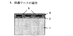
ウエハを処理の間保護するために、保護手段として保護ワニスをウエハの前側に適用することができ、前記保護ワニスは処理後に再度除去される(ワニス除去)。 In order to protect the wafer during processing, a protective varnish can be applied to the front side of the wafer as protective means, and the protective varnish is removed again after processing (varnish removal).
エッチング処理の間に半導体基板が薄くなるのを回避するために、ポケット・ボアをレーザ穴開けする前に、ウエハの後側をインジウム錫酸化物(ITO)で被覆することができ、前記ITOはプラズマ・エッチング後に再度簡単に除去される。 To avoid thinning the semiconductor substrate during the etching process, the back side of the wafer can be coated with indium tin oxide (ITO) before laser drilling the pocket bore, the ITO being It is easily removed again after plasma etching.
SiC基板材料の場合には、残渣を除去するためのウエハの洗浄は、実際には緩衝フッ化水素酸で達成される。 In the case of SiC substrate material, cleaning of the wafer to remove residues is actually accomplished with buffered hydrofluoric acid.
半導体基板のための材料選択性エッチング処理としては、ICP(誘導結合プラズマ)エッチング処理が特に好ましく、層スタックに対しては、それはRIE(反応性イオン・エッチング)処理である。 As a material selective etching process for a semiconductor substrate, an ICP (Inductively Coupled Plasma) etching process is particularly preferred, and for a layer stack it is a RIE (Reactive Ion Etching) process.
レーザとしては、UVレーザが適しており、波長355nmを持つ3倍周波数のNd:YAGレーザが好ましい。 As the laser, a UV laser is suitable, and a triple frequency Nd: YAG laser having a wavelength of 355 nm is preferable.
マイクロ・ビア内へのめっきベースの適用はいくつかの方法で行うことができる。傾斜気相堆積法が好ましく、化学浴堆積法(無電流)またはスパッタリングによる適用もまた可能である。 The application of the plating base within the micro via can be done in several ways. Inclined vapor deposition is preferred, and chemical bath deposition (no current) or sputtering applications are also possible.
必要とあれば、マイクロ・ビアの位置において、脱濡れ層を用いて金層をさらに被覆することができる。脱濡れ層のためにチタンを用いるのが適切であり、この場合、チタンはスパッタリングによって堆積させることができる。脱濡れ層はシャドウ・マスクを用いて効果的に被覆される。 If necessary, the gold layer can be further coated with a dewetting layer at the location of the micro via. Suitably, titanium is used for the dewetting layer, in which case titanium can be deposited by sputtering. The dewetting layer is effectively coated using a shadow mask.
本方法は、硬く化学的に不活性な基板材料内に、実質的に短縮された時間内に高精度でマイクロ・ビアを形成することができるという利点を有する。 The method has the advantage that micro-vias can be formed with high accuracy in a hard and chemically inert substrate material in a substantially shortened time.
本発明の方法によると、UVレーザ放射による材料のマイクロマシニングはプラズマ・エッチングと組み合わされ、構成要素の製作において直接のテクスチャ化のために使用される。ウエハ貫通ビア(または中空リベット・ビア)の形成とは対照的に、材料の完全な貫通はない。残りの材料は、材料選択性の方法で、前側のコンタクトまでプラズマ・エッチングすることによって除去される。このことの特有の利点は、耐久性のエッチング・マスクをリソグラフィ法で製作する必要がなく、レーザ穴開けされたホールがエッチング・マスクの役割を果たすことである。加工されている側が適切な方法で保護されると、材料密度は維持される。この場合、レーザによって穴開けされている保護層は、プラズマ・エッチングの間に平面部の材料が除去されるのを防止する。保護層が使用されないと、広い範囲にわたってエッチングによる材料の除去が生じる。材料厚さの同時に生じる減少は既知のエッチング速度を考慮して推定することができる。 According to the method of the present invention, micromachining of materials by UV laser radiation is combined with plasma etching and used for direct texturing in component fabrication. In contrast to the formation of through-wafer vias (or hollow rivet vias), there is no complete penetration of the material. The remaining material is removed by plasma etching to the front contact in a material selective manner. The particular advantage of this is that a durable etching mask does not have to be produced by lithography, and the laser drilled holes act as an etching mask. If the side being processed is protected in an appropriate manner, the material density is maintained. In this case, the protective layer drilled by the laser prevents the planar material from being removed during plasma etching. If no protective layer is used, material removal by etching occurs over a wide area. The concomitant reduction in material thickness can be estimated considering the known etch rate.
これ以降において、本発明は例示的実施形態を参照して詳細に説明されることになる。関連する概略的図面は、本発明の方法、例えば、GaN高性能電界効果トランジスタまたはMMICのための炭化シリコン(SiC)内のマイクロ・ビアの製作の段階を示す。 In the following, the present invention will be described in detail with reference to exemplary embodiments. The associated schematic drawings show the stages of fabrication of the micro-vias in silicon carbide (SiC) for the method of the present invention, eg, GaN high performance field effect transistors or MMICs.
図1は、トランジスタ構成を備えるウエハの断面を示す。ウエハは、約250〜400μmの厚さを有するSiC基板1で構成され、その上に、約2〜3μmの厚さを有するAlGaN/GaN層スタック2がエピタキシャル成長されている。ウエハの前側上の層スタック2上にはトランジスタの接続コンタクト、すなわちドレイン・コンタクト3、ゲート・コンタクト4およびソース・コンタクト5がある。前側上のソース・コンタクト5がウエハの後側上の接地電極6へ電気的に接続されるように、ソース・コンタクトの電位はウエハの後側(接地電極6)へ戻さなければならず、このことは、金属化されたホール壁8を有するマイクロ・ビア7の支援により達成される。
FIG. 1 shows a cross section of a wafer with a transistor configuration. The wafer is composed of a
下記は、本発明による方法の処理制御および達成される結果の記載である。図2から8は処理手順の概略説明図である。ウエハ・アセンブリ内の完全に処理されたGaNトランジスタまたはMMICにはマイクロ・ビア7が付与される。後に続く処理ステップの間ウエハを保護するために、最初に保護ワニス9がウエハの前側に適用される(図2)。その次に、後側の広い領域がインジウム錫酸化物(ITO)の保護層10で被覆され、前記層は2μmの厚さを有する。しかしながら、このステップは、マイクロ・ビア7がテクスチャ化されている時に、ウエハの厚さが変化しないために必要なだけである。その時、この保護層10はエッチングの間SiC表面の保護としての役割を果たし、後に続くレーザ穴開けの間に、ビアの入口開口部においてはまた除去されることになる。次いで、ウエハの後側からポケット・ホール11の穴開けをするためにレーザが使用される(図4)。所望のポケット・ホール11を形成するために、約15μmの直径を有するレーザ・ビームがウエハの全域にわたって適切に動かされる。ビームの移動およびレーザのパラメータは、SiC/GaN境界表面の近傍においてできるだけ最も平坦な局所的外形が生成されるように、調節することができる。
The following is a description of process control and results achieved of the method according to the invention. 2 to 8 are schematic explanatory diagrams of the processing procedure.
その次に、穴開け作業の間に試料上に堆積した可能性のある遊離粒子(残渣)は、湿式化学反応を用いる洗浄ステップによって除去される。これは、緩衝フッ化水素酸中で超音波を用いるエッチングによって適切に実施される。 Subsequently, free particles (residues) that may have accumulated on the sample during the drilling operation are removed by a cleaning step using a wet chemical reaction. This is suitably performed by etching using ultrasound in buffered hydrofluoric acid.
その次に、レーザによってあらかじめ穴開けされたポケット・ホール11は、乾式化学物質を使用するプラズマ・エッチングによって、前側のコンタクトまで貫通してエッチングされる(図5)。フッ素含有の混合ガス(例えば、六フッ化硫黄/酸素/ヘリウム=SF6/O2/He)中でのICPエッチングによって残りのSiCを除去することは好都合である。エッチング・パラメータ(分圧、温度)を最適化することによって、滑らかなホール壁が達成される。SiC対GaNのエッチング処理の選択比は>100:1であり、すなわち、GaN(厚さ約2〜3μm)上でのエッチング処理が実質的に停止するので、エッチングの良好な均一性をウエハの全域にわたって達成することができる。 Next, the pocket hole 11 previously drilled by the laser is etched through to the front contact by plasma etching using dry chemicals (FIG. 5). It is advantageous to remove the remaining SiC by ICP etching in a fluorine-containing gas mixture (eg, sulfur hexafluoride / oxygen / helium = SF 6 / O 2 / He). By optimizing the etching parameters (partial pressure, temperature), a smooth hole wall is achieved. The selectivity of the SiC to GaN etching process is> 100: 1, ie, the etching process on GaN (about 2-3 μm thick) is substantially stopped, so that good etching uniformity is achieved on the wafer. It can be achieved over the whole area.
2〜3μmの厚さを有するエピタキシャル層(層スタック2)の除去は、例えば、三塩化ホウ素/塩素(BCl3/Cl2)を用いるRIE処理を含むプラズマ化学反応手段によって達成される。GaN対白金の乾式化学反応エッチング処理の選択比は>10:1である。次いで、約5μmの全厚を有する前側コンタクトの金属層はほんの少しずつだけ剥ぎ取られる、すなわち、実際には、エッチング処理は金属層のところで停止する。エッチング不足は生じない。白金コンタクトの下側に設けられ、数10nmの厚さを有するチタン層は剥ぎ取られる。 Removal of the epitaxial layer (layer stack 2) having a thickness of 2-3 μm is achieved by plasma chemical reaction means including, for example, RIE treatment using boron trichloride / chlorine (BCl 3 / Cl 2 ). The selectivity of the dry chemical reaction etching process of GaN to platinum is> 10: 1. The metal layer of the front contact having a total thickness of about 5 μm is then stripped off little by little, ie in practice the etching process stops at the metal layer. Insufficient etching does not occur. The titanium layer provided under the platinum contact and having a thickness of several tens of nm is peeled off.
エッチング処理に続いて、場合によっては適用される層10(ITO)を再び除去することができ、これは塩化第三鉄を用いて効果的に実施される(図6)。 Following the etching process, the optionally applied layer 10 (ITO) can be removed again, which is effectively carried out with ferric chloride (FIG. 6).
その次に、薄い金属層12がウエハの後側に気相堆積される。その際に、この例示的実施形態を参照すると、ホール壁の結合力のある被覆が傾斜気相堆積法によって達成される。スパッタリングまたは無電流化学反応堆積法等の他の金属化処理もまた可能である。その次に、金属層12を用いて得られるめっきベースは、一般的に5μmの厚さを有する電気めっき金層13を適用することによって強化される(図7)。このようにして、ウエハの一方の側からウエハのもう一方の側への電気的接続が、結合力のある金層13を使用して構築される。
A
金属化に続いて、保護ワニスがもう1つの処理ステップの間に剥ぎ取られる(図8)。 Following metallization, the protective varnish is stripped off during another processing step (FIG. 8).
必要ならば、チタンの脱濡れ層14をビア入口開口部のところの後側に適用することもできる、すなわち、チタン層は100nmの厚さを有し、前記層は既存の金層13上にスパッタリングされる。脱濡れ層14はテクスチャ化手法でウエハに適用され、そのため、シャドウ・マスクが使用される。シャドウ・マスクは0.1mmの厚さを有する金属フォイルで構成され、そのため、前記フォイルに開口部を穴開けするためにレーザを使用する。金属フォイル内の開口部の配置はウエハ上のマイクロ・ビア7の配列に対応する。シャドウ・マスク内の開口部の直径は、約40μmの幅を有するチタンの輪がビア入口開口部の周りに形成されるように、ウエハの後側上のマイクロ・ビア7の入口直径よりもわずかに大きい。両方の部品は、シャドウ・マスクおよびウエハの各端部にある4個の追加の貫通ボアを使用して、位置合わせピンで相互に調節される、すなわち、前記部品は一致するように位置合わせされる。
If necessary, a
保護ワニス9はまた、脱濡れ層14(チタン脱濡れ層)の堆積後に剥ぎ取ることもできることに留意すべきである。
It should be noted that the
図9は完成したマイクロ・ビア7の断面の概略図を示す。 FIG. 9 shows a schematic cross section of the completed micro via 7.
エッチング処理の間の材料厚さの制御された減少が容認されるならば、表面のITOによる遮蔽(保護層10)も省略することができる、すなわち、図3および6に従うステップは必要ではない。 If a controlled decrease in material thickness during the etching process is acceptable, the surface ITO shielding (protective layer 10) can also be omitted, ie the steps according to FIGS. 3 and 6 are not necessary.
図10から14はこの場合に適用できる処理手順を示す。この場合、処理ステップは、第1の例の処理ステップ1、3、4、6および7(図2、4、5、7および8に対応)に対応する。 10 to 14 show processing procedures applicable in this case. In this case, the processing steps correspond to the processing steps 1, 3, 4, 6 and 7 (corresponding to FIGS. 2, 4, 5, 7 and 8) of the first example.
この場合、ウエハの全厚さはSiCの広範囲の除去のため減少する。約2時間のエッチング時間を考慮すると、ウエハの厚さは390μmから250〜300μmまで減少する。ホールの底部においては、35〜70μmの縁部長さが得られ、そのため、隅部は六角形状に広げられる。ホールの形状は円錐形で、入口における断面が明らかに広がっており、したがって、ホール壁を金属でその後に被覆することを容易にする。 In this case, the total wafer thickness is reduced due to the extensive removal of SiC. Considering an etch time of about 2 hours, the wafer thickness is reduced from 390 μm to 250-300 μm. At the bottom of the hole, an edge length of 35 to 70 [mu] m is obtained, so that the corners are expanded into a hexagonal shape. The shape of the hole is conical and the cross section at the entrance is clearly enlarged, thus facilitating subsequent coating of the hole wall with metal.
除去速度、融通性および信頼性を考慮すると、3倍周波数のNd:YAGレーザが、非常に硬く化学的に不活性なSiCを加工するのに適している。このレーザは、波長355nmのスペクトルの紫外線領域内で、100kHzまでのパルス周波数を持つ高エネルギーのナノ秒パルスを送出する。レーザ・ビームは、試料テーブルのCNC制御による移動およびガルバノ・スキャナによるビーム偏向を組み合わせることによって、マイクロメータ精度で動かされる。画像認識および高精度空気浮上式XY交差テーブルの使用により、レーザ・ビームは、ワークピース上の既存の構造に対して、±1μmの精度で位置合わせすることができる。この精度は、レーザ・テクスチャ化が後側上で行われ、調節用マークが前側上に置かれている(底部に置かれている)時でさえ、達成される。 In view of removal speed, flexibility and reliability, a triple frequency Nd: YAG laser is suitable for processing very hard and chemically inert SiC. This laser delivers high energy nanosecond pulses with a pulse frequency up to 100 kHz in the ultraviolet region of the spectrum with a wavelength of 355 nm. The laser beam is moved with micrometer accuracy by combining CNC controlled movement of the sample table and beam deflection with a galvano scanner. Through the use of image recognition and a high precision air levitation XY intersection table, the laser beam can be aligned to an existing structure on the workpiece with an accuracy of ± 1 μm. This accuracy is achieved even when laser texturing is performed on the rear side and the adjustment mark is placed on the front side (placed on the bottom).
矩形断面およびできる限り平坦なホール底部を有するポケット・ホールを穴開けするために、レーザが使用された。縁部長さは、レーザ入口開口部においては約75μmであり、ホール底部においては約15μmであって、ホール底部の下側には約40μmのSiCが残された。 A laser was used to drill a pocket hole with a rectangular cross section and the flatest hole bottom possible. The edge length was about 75 μm at the laser entrance opening and about 15 μm at the bottom of the hole, leaving about 40 μm of SiC under the bottom of the hole.
自動化された穴開け処理が使用され、そのため、試料テーブルがマイクロメータ精度で正確に動かされて、試料のそれぞれの加工場所がビーム出口の下側に位置合わせされ、次いで、レーザ・ビームがミラー装置(ガルバノ・スキャナ)を用いてワークピース上を急速に動かされ、そのために、250〜450μmの厚さを有するSiCが使用された。走査型電子顕微鏡で観察すると、レーザ穴開けされたホールはわずかに円錐状であり、堆積物が最小の滑らかな壁を形成できることを容易に見ることができる。 An automated drilling process is used, so that the sample table is moved accurately with micrometer accuracy, the respective processing location of the sample is aligned below the beam exit, and then the laser beam is mirrored (Galvano scanner) was used to move rapidly over the workpiece, for which purpose SiC with a thickness of 250-450 μm was used. When viewed with a scanning electron microscope, the laser drilled holes are slightly conical and it can easily be seen that the deposits can form a smooth wall with minimal.
SiC試料上で行われた抵抗測定により、2つの場所の間で低オーム接続を構築できることが確認された。そうするために、最初に試料の1つの側の表面全体が、5μmの厚さを有する金層を用いて金属化された。次いで、もう一方の側から、ビアの行列が上記のように穴開けされた。ホール間の間隔は500μmであった。単一のホールを貫通する抵抗を測定する前に、個々のホールを相互に電気的に分離する必要があった。これを達成するために、金層は、500×500μm2の寸法を有し、各々が1つのビアを有する領域を得るために分断された(線引きされた)。SiC試料を貫通する非常に均一なコンタクトを、良好な再現性をもって実証することができた。抵抗値は25〜31mΩである。206個のマイクロ・ビアにわたる平均値は27±2mΩである。実施可能な中空リベットは3〜4のアスペクト比を示す。 Resistance measurements made on SiC samples confirmed that a low ohmic connection can be established between the two locations. To do so, first the entire surface on one side of the sample was metallized with a gold layer having a thickness of 5 μm. Then, from the other side, a via matrix was drilled as described above. The distance between the holes was 500 μm. Prior to measuring the resistance through a single hole, it was necessary to electrically isolate the individual holes from each other. In order to achieve this, the gold layer had dimensions of 500 × 500 μm 2 and was cut (drawn) to obtain areas each having one via. A very uniform contact through the SiC sample could be demonstrated with good reproducibility. The resistance value is 25 to 31 mΩ. The average value over 206 micro vias is 27 ± 2 mΩ. Possible hollow rivets exhibit an aspect ratio of 3-4.
異なるタイプの構成トランジスタでの試験において、デバイスの機能性が実証された。トランジスタの特性線を参照して、GaN処理技術においてレーザ穴開けマイクロ・ビアを首尾よく実施できることが証明された。 Device functionality has been demonstrated in tests with different types of constituent transistors. With reference to transistor characteristic lines, it has been demonstrated that laser drilling micro-vias can be successfully implemented in GaN processing technology.
技術的な検討は、高性能GaN電界効果トランジスタのための単結晶SiCウエハ材料を貫通するレーザ穴開けマイクロ・ビアを実施できることを示している。デバイス処理技術においてレーザ生成のマイクロ・テクスチャ化を首尾よく実施できることの証明を与えることができた。 Technical considerations have shown that laser drilled micro vias can be implemented through single crystal SiC wafer materials for high performance GaN field effect transistors. It was possible to prove that laser-generated microtexturing can be successfully implemented in device processing technology.
半導体ウエハの処理におけるレーザ・マイクロマシニングの適用のための必須条件は、±1μm以上のビーム中心の高い位置合わせ精度である。この精度は既存のデバイス構造に対するビーム位置合わせに関連し、前側の加工時にもおよび後側の加工時にも達成されなければならない。 A prerequisite for the application of laser micromachining in the processing of semiconductor wafers is a high alignment accuracy of the beam center of ± 1 μm or more. This accuracy is related to beam alignment relative to existing device structures and must be achieved both during front side processing and during back side processing.
本発明は、非常に硬く、化学的に安定な炭化シリコンの貫通ホールめっきを可能とする。そのために3〜4のアスペクト比が実証された。 The present invention enables through hole plating of very hard and chemically stable silicon carbide. Therefore, an aspect ratio of 3-4 was demonstrated.
1 SiC基板
2 AlGaN/GaN層スタック
3 ドレイン・コンタクト
4 ゲート・コンタクト
5 ソース・コンタクト
6 接地電極
7 マイクロ・ビア
8 ホール壁
9 保護ワニス
10 保護層(ITO)
11 ポケット・ホール
12 金属層
13 金層
14 脱濡れ層
DESCRIPTION OF
11
Claims (14)
前記コンタクト位置において前記半導体ウエハの前記後側から半導体基板内へポケット・ホールをレーザ穴開けする第1のステップと、
前記半導体ウエハを洗浄する第2のステップと、
前記ポケット・ホールが前記半導体ウエハの活性層スタックまで貫通するように前記半導体基板を選択的にプラズマ・エッチングする第3のステップと、
前記ポケット・ホールが前記コンタクトに到達するように前記半導体ウエハの前記活性層スタックを選択的にプラズマ・エッチングする第4のステップと、
前記半導体ウエハの前記後側および前記ポケット・ホールの内側にめっきベースを適用する第5のステップと
前記半導体ウエハの前記後側および前記ポケット・ホールの内壁をめっきすることによって金を適用するステップと
を具備することを特徴とする方法。Through the semi-conductor wafer to a method of making a vertical through plated holes for the fabrication of semiconductor devices extending to the rear from the front side of the contact of the semiconductor wafer,
A first step of laser drilling a pocket hole into the semiconductor substrate from the back side of the semiconductor wafer at the contact location;
A second step of cleaning the semiconductor wafer;
A third step of selectively plasma etching the semiconductor substrate such that the pocket holes penetrate to the active layer stack of the semiconductor wafer;
A fourth step of selectively plasma etching the active layer stack of the semiconductor wafer such that the pocket hole reaches the contact;
Applying a gold by plating the rear side and the fifth step and the inner wall of the rear side and the pocket holes of the semiconductor wafer to apply plating base on the inside of the pocket holes of the semiconductor wafer A method comprising the steps of:
Applications Claiming Priority (3)
| Application Number | Priority Date | Filing Date | Title |
|---|---|---|---|
| DE102005042074.5 | 2005-08-31 | ||
| DE102005042074A DE102005042074A1 (en) | 2005-08-31 | 2005-08-31 | Method for producing plated-through holes in semiconductor wafers |
| PCT/EP2006/064599 WO2007025812A1 (en) | 2005-08-31 | 2006-07-24 | Method for producing through-contacts in semi-conductor wafers |
Publications (2)
| Publication Number | Publication Date |
|---|---|
| JP2009506561A JP2009506561A (en) | 2009-02-12 |
| JP5123185B2 true JP5123185B2 (en) | 2013-01-16 |
Family
ID=37076379
Family Applications (1)
| Application Number | Title | Priority Date | Filing Date |
|---|---|---|---|
| JP2008528445A Expired - Fee Related JP5123185B2 (en) | 2005-08-31 | 2006-07-24 | Through-hole plating method for semiconductor wafer |
Country Status (5)
| Country | Link |
|---|---|
| US (1) | US8455355B2 (en) |
| EP (1) | EP1920461B1 (en) |
| JP (1) | JP5123185B2 (en) |
| DE (1) | DE102005042074A1 (en) |
| WO (1) | WO2007025812A1 (en) |
Families Citing this family (31)
| Publication number | Priority date | Publication date | Assignee | Title |
|---|---|---|---|---|
| US8084866B2 (en) | 2003-12-10 | 2011-12-27 | Micron Technology, Inc. | Microelectronic devices and methods for filling vias in microelectronic devices |
| US7091124B2 (en) | 2003-11-13 | 2006-08-15 | Micron Technology, Inc. | Methods for forming vias in microelectronic devices, and methods for packaging microelectronic devices |
| US20050247894A1 (en) | 2004-05-05 | 2005-11-10 | Watkins Charles M | Systems and methods for forming apertures in microfeature workpieces |
| US7232754B2 (en) | 2004-06-29 | 2007-06-19 | Micron Technology, Inc. | Microelectronic devices and methods for forming interconnects in microelectronic devices |
| US7083425B2 (en) | 2004-08-27 | 2006-08-01 | Micron Technology, Inc. | Slanted vias for electrical circuits on circuit boards and other substrates |
| US7300857B2 (en) | 2004-09-02 | 2007-11-27 | Micron Technology, Inc. | Through-wafer interconnects for photoimager and memory wafers |
| US7271482B2 (en) | 2004-12-30 | 2007-09-18 | Micron Technology, Inc. | Methods for forming interconnects in microelectronic workpieces and microelectronic workpieces formed using such methods |
| US7795134B2 (en) | 2005-06-28 | 2010-09-14 | Micron Technology, Inc. | Conductive interconnect structures and formation methods using supercritical fluids |
| US7863187B2 (en) | 2005-09-01 | 2011-01-04 | Micron Technology, Inc. | Microfeature workpieces and methods for forming interconnects in microfeature workpieces |
| US7262134B2 (en) | 2005-09-01 | 2007-08-28 | Micron Technology, Inc. | Microfeature workpieces and methods for forming interconnects in microfeature workpieces |
| US7749899B2 (en) | 2006-06-01 | 2010-07-06 | Micron Technology, Inc. | Microelectronic workpieces and methods and systems for forming interconnects in microelectronic workpieces |
| US7629249B2 (en) | 2006-08-28 | 2009-12-08 | Micron Technology, Inc. | Microfeature workpieces having conductive interconnect structures formed by chemically reactive processes, and associated systems and methods |
| US7902643B2 (en) | 2006-08-31 | 2011-03-08 | Micron Technology, Inc. | Microfeature workpieces having interconnects and conductive backplanes, and associated systems and methods |
| DE102007019552B4 (en) * | 2007-04-25 | 2009-12-17 | Infineon Technologies Ag | Method for producing a substrate with feedthrough and substrate and semiconductor module with feedthrough |
| JP5228381B2 (en) * | 2007-06-25 | 2013-07-03 | 三菱電機株式会社 | Manufacturing method of semiconductor device |
| SG149710A1 (en) | 2007-07-12 | 2009-02-27 | Micron Technology Inc | Interconnects for packaged semiconductor devices and methods for manufacturing such devices |
| SG150410A1 (en) | 2007-08-31 | 2009-03-30 | Micron Technology Inc | Partitioned through-layer via and associated systems and methods |
| US7884015B2 (en) | 2007-12-06 | 2011-02-08 | Micron Technology, Inc. | Methods for forming interconnects in microelectronic workpieces and microelectronic workpieces formed using such methods |
| CA2708114C (en) * | 2009-06-18 | 2017-11-14 | Lin-ping SHEN | Butler matrix and beam forming antenna comprising same |
| US20110209432A1 (en) * | 2010-03-01 | 2011-09-01 | Downey Mike A | Metal "slip clip" to hold metal studes in top track of commercial interior framing |
| CN101916754B (en) * | 2010-06-29 | 2012-08-29 | 香港应用科技研究院有限公司 | Through-hole, through-hole forming method and through-hole filling method |
| JP5566803B2 (en) * | 2010-07-21 | 2014-08-06 | 住友電工デバイス・イノベーション株式会社 | Manufacturing method of semiconductor device |
| KR101219386B1 (en) * | 2011-02-16 | 2013-01-21 | 한국기계연구원 | Fabricating method of through silicon via and semiconductor chip manufactured by the same |
| JP2013058624A (en) * | 2011-09-08 | 2013-03-28 | Mitsubishi Electric Corp | Manufacturing method of laser diode element |
| CN102768950A (en) * | 2012-07-12 | 2012-11-07 | 江苏扬景光电有限公司 | Method for forming holes in substrate of nitride device by mixing type etching |
| KR101988893B1 (en) * | 2012-12-12 | 2019-09-30 | 한국전자통신연구원 | Semiconductor device and a method of manufacturing the same |
| JP6309211B2 (en) * | 2013-06-14 | 2018-04-11 | 新電元工業株式会社 | Silicon carbide semiconductor device |
| JP2015002299A (en) * | 2013-06-17 | 2015-01-05 | 株式会社ザイキューブ | Funnel-shaped through electrode and manufacturing method therefor |
| CN107980171B (en) * | 2016-12-23 | 2022-06-24 | 苏州能讯高能半导体有限公司 | Semiconductor chip, semiconductor wafer, and method for manufacturing semiconductor wafer |
| US10269756B2 (en) * | 2017-04-21 | 2019-04-23 | Invensas Bonding Technologies, Inc. | Die processing |
| JP7076576B2 (en) * | 2018-12-27 | 2022-05-27 | 三菱電機株式会社 | Semiconductor device structure |
Family Cites Families (20)
| Publication number | Priority date | Publication date | Assignee | Title |
|---|---|---|---|---|
| US4473737A (en) * | 1981-09-28 | 1984-09-25 | General Electric Company | Reverse laser drilling |
| US4897708A (en) * | 1986-07-17 | 1990-01-30 | Laser Dynamics, Inc. | Semiconductor wafer array |
| US5371042A (en) * | 1992-06-16 | 1994-12-06 | Applied Materials, Inc. | Method of filling contacts in semiconductor devices |
| JP3724110B2 (en) * | 1997-04-24 | 2005-12-07 | 三菱電機株式会社 | Manufacturing method of semiconductor device |
| JP4264992B2 (en) * | 1997-05-28 | 2009-05-20 | ソニー株式会社 | Manufacturing method of semiconductor device |
| US6239033B1 (en) | 1998-05-28 | 2001-05-29 | Sony Corporation | Manufacturing method of semiconductor device |
| JP2868008B1 (en) * | 1997-11-21 | 1999-03-10 | 日本電気株式会社 | Semiconductor device and manufacturing method thereof |
| DE69737262T2 (en) * | 1997-11-26 | 2007-11-08 | Stmicroelectronics S.R.L., Agrate Brianza | A method of manufacturing a front-to-back via in micro-integrated circuits |
| JPH11238870A (en) * | 1998-02-20 | 1999-08-31 | Nec Corp | Semiconductor device and manufacture thereof |
| US6475889B1 (en) * | 2000-04-11 | 2002-11-05 | Cree, Inc. | Method of forming vias in silicon carbide and resulting devices and circuits |
| US7125786B2 (en) * | 2000-04-11 | 2006-10-24 | Cree, Inc. | Method of forming vias in silicon carbide and resulting devices and circuits |
| US20020086520A1 (en) * | 2001-01-02 | 2002-07-04 | Advanced Semiconductor Engineering Inc. | Semiconductor device having bump electrode |
| CA2436736A1 (en) * | 2001-01-31 | 2002-08-08 | Electro Scientific Industries, Inc. | Ultraviolet laser ablative patterning of microstructures in semiconductors |
| US7233028B2 (en) * | 2001-02-23 | 2007-06-19 | Nitronex Corporation | Gallium nitride material devices and methods of forming the same |
| JP4053257B2 (en) * | 2001-06-14 | 2008-02-27 | 新光電気工業株式会社 | Manufacturing method of semiconductor device |
| US6902872B2 (en) * | 2002-07-29 | 2005-06-07 | Hewlett-Packard Development Company, L.P. | Method of forming a through-substrate interconnect |
| US6903442B2 (en) * | 2002-08-29 | 2005-06-07 | Micron Technology, Inc. | Semiconductor component having backside pin contacts |
| US6936536B2 (en) * | 2002-10-09 | 2005-08-30 | Micron Technology, Inc. | Methods of forming conductive through-wafer vias |
| US6841883B1 (en) * | 2003-03-31 | 2005-01-11 | Micron Technology, Inc. | Multi-dice chip scale semiconductor components and wafer level methods of fabrication |
| US7674719B2 (en) * | 2005-08-01 | 2010-03-09 | Panasonic Corporation | Via hole machining for microwave monolithic integrated circuits |
-
2005
- 2005-08-31 DE DE102005042074A patent/DE102005042074A1/en not_active Withdrawn
-
2006
- 2006-07-24 EP EP06792559.4A patent/EP1920461B1/en not_active Not-in-force
- 2006-07-24 US US11/993,459 patent/US8455355B2/en active Active
- 2006-07-24 WO PCT/EP2006/064599 patent/WO2007025812A1/en active Application Filing
- 2006-07-24 JP JP2008528445A patent/JP5123185B2/en not_active Expired - Fee Related
Also Published As
| Publication number | Publication date |
|---|---|
| EP1920461A1 (en) | 2008-05-14 |
| US20080286963A1 (en) | 2008-11-20 |
| DE102005042074A1 (en) | 2007-03-08 |
| US8455355B2 (en) | 2013-06-04 |
| WO2007025812A1 (en) | 2007-03-08 |
| EP1920461B1 (en) | 2016-11-16 |
| JP2009506561A (en) | 2009-02-12 |
Similar Documents
| Publication | Publication Date | Title |
|---|---|---|
| JP5123185B2 (en) | Through-hole plating method for semiconductor wafer | |
| JP5080456B2 (en) | Method for making vertical electrical contact connection in a semiconductor wafer | |
| JP5022683B2 (en) | Manufacturing method of semiconductor device | |
| JPH06505833A (en) | Integrated circuit board with multichip module and planarized patterned surface | |
| KR101117573B1 (en) | Fabrication Method of Through Silicon Via using Hybrid process | |
| KR100345622B1 (en) | Method for forming pattern of metal film | |
| JP2006261553A (en) | Semiconductor device and its manufacturing method | |
| Kim et al. | SiC via holes by laser drilling | |
| US9105710B2 (en) | Wafer dicing method for improving die packaging quality | |
| US20130288489A1 (en) | Method and Apparatus to Fabricate Vias in Substrates for Gallium Nitride MMICs | |
| US20220375787A1 (en) | Methods of micro-via formation for advanced packaging | |
| Kim et al. | High-rate laser ablation for through-wafer via holes in SiC substrates and GaN/AlN/SiC Templates | |
| JP2000164569A (en) | Manufacture of semiconductor device | |
| KR20100023805A (en) | Conductive via formation | |
| JPH118249A (en) | Manufacture of wiring | |
| JP3306889B2 (en) | Method for manufacturing semiconductor device | |
| KR100593211B1 (en) | Method for manufacturing through hole electrode for wafer | |
| JP2009158543A (en) | Method of manufacturing semiconductor device | |
| Huang | Laser Drilling & Plasma Descum Employed In The Process of Wafer-Level Chip Scale Package (WLCSP) | |
| JP2023111336A (en) | Tungsten blanks for manufacturing through workpiece of tungsten and method for manufacturing through workpiece of tungsten using tungsten blanks | |
| TWM613899U (en) | Circuit board | |
| CN116851940A (en) | Novel passivation layer perforating method | |
| JPH04170031A (en) | Formation of metal interconnection | |
| JP2006222154A (en) | Method for manufacturing semiconductor device | |
| JPH0645453A (en) | Manufacture of semiconductor device |
Legal Events
| Date | Code | Title | Description |
|---|---|---|---|
| A621 | Written request for application examination |
Free format text: JAPANESE INTERMEDIATE CODE: A621 Effective date: 20090514 |
|
| A131 | Notification of reasons for refusal |
Free format text: JAPANESE INTERMEDIATE CODE: A131 Effective date: 20120209 |
|
| A601 | Written request for extension of time |
Free format text: JAPANESE INTERMEDIATE CODE: A601 Effective date: 20120424 |
|
| A602 | Written permission of extension of time |
Free format text: JAPANESE INTERMEDIATE CODE: A602 Effective date: 20120502 |
|
| A521 | Request for written amendment filed |
Free format text: JAPANESE INTERMEDIATE CODE: A523 Effective date: 20120607 |
|
| TRDD | Decision of grant or rejection written | ||
| A01 | Written decision to grant a patent or to grant a registration (utility model) |
Free format text: JAPANESE INTERMEDIATE CODE: A01 Effective date: 20121009 |
|
| A01 | Written decision to grant a patent or to grant a registration (utility model) |
Free format text: JAPANESE INTERMEDIATE CODE: A01 |
|
| A61 | First payment of annual fees (during grant procedure) |
Free format text: JAPANESE INTERMEDIATE CODE: A61 Effective date: 20121025 |
|
| FPAY | Renewal fee payment (event date is renewal date of database) |
Free format text: PAYMENT UNTIL: 20151102 Year of fee payment: 3 |
|
| R150 | Certificate of patent or registration of utility model |
Free format text: JAPANESE INTERMEDIATE CODE: R150 Ref document number: 5123185 Country of ref document: JP Free format text: JAPANESE INTERMEDIATE CODE: R150 |
|
| R250 | Receipt of annual fees |
Free format text: JAPANESE INTERMEDIATE CODE: R250 |
|
| R250 | Receipt of annual fees |
Free format text: JAPANESE INTERMEDIATE CODE: R250 |
|
| R250 | Receipt of annual fees |
Free format text: JAPANESE INTERMEDIATE CODE: R250 |
|
| R250 | Receipt of annual fees |
Free format text: JAPANESE INTERMEDIATE CODE: R250 |
|
| R250 | Receipt of annual fees |
Free format text: JAPANESE INTERMEDIATE CODE: R250 |
|
| R250 | Receipt of annual fees |
Free format text: JAPANESE INTERMEDIATE CODE: R250 |
|
| R250 | Receipt of annual fees |
Free format text: JAPANESE INTERMEDIATE CODE: R250 |
|
| S111 | Request for change of ownership or part of ownership |
Free format text: JAPANESE INTERMEDIATE CODE: R313113 |
|
| S631 | Written request for registration of reclamation of domicile |
Free format text: JAPANESE INTERMEDIATE CODE: R313631 |
|
| S633 | Written request for registration of reclamation of name |
Free format text: JAPANESE INTERMEDIATE CODE: R313633 |
|
| LAPS | Cancellation because of no payment of annual fees | ||
| R350 | Written notification of registration of transfer |
Free format text: JAPANESE INTERMEDIATE CODE: R350 |