JP5122192B2 - Semiconductor device mounting equipment - Google Patents
Semiconductor device mounting equipment Download PDFInfo
- Publication number
- JP5122192B2 JP5122192B2 JP2007176209A JP2007176209A JP5122192B2 JP 5122192 B2 JP5122192 B2 JP 5122192B2 JP 2007176209 A JP2007176209 A JP 2007176209A JP 2007176209 A JP2007176209 A JP 2007176209A JP 5122192 B2 JP5122192 B2 JP 5122192B2
- Authority
- JP
- Japan
- Prior art keywords
- semiconductor element
- elastomer
- heating
- pressing
- mounting apparatus
- Prior art date
- Legal status (The legal status is an assumption and is not a legal conclusion. Google has not performed a legal analysis and makes no representation as to the accuracy of the status listed.)
- Expired - Fee Related
Links
Images


Classifications
-
- B—PERFORMING OPERATIONS; TRANSPORTING
- B30—PRESSES
- B30B—PRESSES IN GENERAL
- B30B5/00—Presses characterised by the use of pressing means other than those mentioned in the preceding groups
- B30B5/02—Presses characterised by the use of pressing means other than those mentioned in the preceding groups wherein the pressing means is in the form of a flexible element, e.g. diaphragm, urged by fluid pressure
-
- B—PERFORMING OPERATIONS; TRANSPORTING
- B30—PRESSES
- B30B—PRESSES IN GENERAL
- B30B15/00—Details of, or accessories for, presses; Auxiliary measures in connection with pressing
- B30B15/06—Platens or press rams
- B30B15/065—Press rams
-
- H—ELECTRICITY
- H01—ELECTRIC ELEMENTS
- H01L—SEMICONDUCTOR DEVICES NOT COVERED BY CLASS H10
- H01L24/00—Arrangements for connecting or disconnecting semiconductor or solid-state bodies; Methods or apparatus related thereto
- H01L24/01—Means for bonding being attached to, or being formed on, the surface to be connected, e.g. chip-to-package, die-attach, "first-level" interconnects; Manufacturing methods related thereto
- H01L24/26—Layer connectors, e.g. plate connectors, solder or adhesive layers; Manufacturing methods related thereto
- H01L24/31—Structure, shape, material or disposition of the layer connectors after the connecting process
- H01L24/32—Structure, shape, material or disposition of the layer connectors after the connecting process of an individual layer connector
-
- H—ELECTRICITY
- H01—ELECTRIC ELEMENTS
- H01L—SEMICONDUCTOR DEVICES NOT COVERED BY CLASS H10
- H01L24/00—Arrangements for connecting or disconnecting semiconductor or solid-state bodies; Methods or apparatus related thereto
- H01L24/74—Apparatus for manufacturing arrangements for connecting or disconnecting semiconductor or solid-state bodies
- H01L24/75—Apparatus for connecting with bump connectors or layer connectors
-
- H—ELECTRICITY
- H01—ELECTRIC ELEMENTS
- H01L—SEMICONDUCTOR DEVICES NOT COVERED BY CLASS H10
- H01L24/00—Arrangements for connecting or disconnecting semiconductor or solid-state bodies; Methods or apparatus related thereto
- H01L24/80—Methods for connecting semiconductor or other solid state bodies using means for bonding being attached to, or being formed on, the surface to be connected
- H01L24/81—Methods for connecting semiconductor or other solid state bodies using means for bonding being attached to, or being formed on, the surface to be connected using a bump connector
-
- H—ELECTRICITY
- H01—ELECTRIC ELEMENTS
- H01L—SEMICONDUCTOR DEVICES NOT COVERED BY CLASS H10
- H01L24/00—Arrangements for connecting or disconnecting semiconductor or solid-state bodies; Methods or apparatus related thereto
- H01L24/80—Methods for connecting semiconductor or other solid state bodies using means for bonding being attached to, or being formed on, the surface to be connected
- H01L24/83—Methods for connecting semiconductor or other solid state bodies using means for bonding being attached to, or being formed on, the surface to be connected using a layer connector
-
- H—ELECTRICITY
- H01—ELECTRIC ELEMENTS
- H01L—SEMICONDUCTOR DEVICES NOT COVERED BY CLASS H10
- H01L2224/00—Indexing scheme for arrangements for connecting or disconnecting semiconductor or solid-state bodies and methods related thereto as covered by H01L24/00
- H01L2224/01—Means for bonding being attached to, or being formed on, the surface to be connected, e.g. chip-to-package, die-attach, "first-level" interconnects; Manufacturing methods related thereto
- H01L2224/10—Bump connectors; Manufacturing methods related thereto
- H01L2224/15—Structure, shape, material or disposition of the bump connectors after the connecting process
- H01L2224/16—Structure, shape, material or disposition of the bump connectors after the connecting process of an individual bump connector
- H01L2224/161—Disposition
- H01L2224/16151—Disposition the bump connector connecting between a semiconductor or solid-state body and an item not being a semiconductor or solid-state body, e.g. chip-to-substrate, chip-to-passive
- H01L2224/16221—Disposition the bump connector connecting between a semiconductor or solid-state body and an item not being a semiconductor or solid-state body, e.g. chip-to-substrate, chip-to-passive the body and the item being stacked
- H01L2224/16225—Disposition the bump connector connecting between a semiconductor or solid-state body and an item not being a semiconductor or solid-state body, e.g. chip-to-substrate, chip-to-passive the body and the item being stacked the item being non-metallic, e.g. insulating substrate with or without metallisation
-
- H—ELECTRICITY
- H01—ELECTRIC ELEMENTS
- H01L—SEMICONDUCTOR DEVICES NOT COVERED BY CLASS H10
- H01L2224/00—Indexing scheme for arrangements for connecting or disconnecting semiconductor or solid-state bodies and methods related thereto as covered by H01L24/00
- H01L2224/01—Means for bonding being attached to, or being formed on, the surface to be connected, e.g. chip-to-package, die-attach, "first-level" interconnects; Manufacturing methods related thereto
- H01L2224/26—Layer connectors, e.g. plate connectors, solder or adhesive layers; Manufacturing methods related thereto
- H01L2224/31—Structure, shape, material or disposition of the layer connectors after the connecting process
- H01L2224/32—Structure, shape, material or disposition of the layer connectors after the connecting process of an individual layer connector
- H01L2224/321—Disposition
- H01L2224/32151—Disposition the layer connector connecting between a semiconductor or solid-state body and an item not being a semiconductor or solid-state body, e.g. chip-to-substrate, chip-to-passive
- H01L2224/32221—Disposition the layer connector connecting between a semiconductor or solid-state body and an item not being a semiconductor or solid-state body, e.g. chip-to-substrate, chip-to-passive the body and the item being stacked
- H01L2224/32225—Disposition the layer connector connecting between a semiconductor or solid-state body and an item not being a semiconductor or solid-state body, e.g. chip-to-substrate, chip-to-passive the body and the item being stacked the item being non-metallic, e.g. insulating substrate with or without metallisation
-
- H—ELECTRICITY
- H01—ELECTRIC ELEMENTS
- H01L—SEMICONDUCTOR DEVICES NOT COVERED BY CLASS H10
- H01L2224/00—Indexing scheme for arrangements for connecting or disconnecting semiconductor or solid-state bodies and methods related thereto as covered by H01L24/00
- H01L2224/73—Means for bonding being of different types provided for in two or more of groups H01L2224/10, H01L2224/18, H01L2224/26, H01L2224/34, H01L2224/42, H01L2224/50, H01L2224/63, H01L2224/71
- H01L2224/732—Location after the connecting process
- H01L2224/73201—Location after the connecting process on the same surface
- H01L2224/73203—Bump and layer connectors
- H01L2224/73204—Bump and layer connectors the bump connector being embedded into the layer connector
-
- H—ELECTRICITY
- H01—ELECTRIC ELEMENTS
- H01L—SEMICONDUCTOR DEVICES NOT COVERED BY CLASS H10
- H01L2224/00—Indexing scheme for arrangements for connecting or disconnecting semiconductor or solid-state bodies and methods related thereto as covered by H01L24/00
- H01L2224/74—Apparatus for manufacturing arrangements for connecting or disconnecting semiconductor or solid-state bodies and for methods related thereto
- H01L2224/75—Apparatus for connecting with bump connectors or layer connectors
- H01L2224/7525—Means for applying energy, e.g. heating means
- H01L2224/75252—Means for applying energy, e.g. heating means in the upper part of the bonding apparatus, e.g. in the bonding head
-
- H—ELECTRICITY
- H01—ELECTRIC ELEMENTS
- H01L—SEMICONDUCTOR DEVICES NOT COVERED BY CLASS H10
- H01L2224/00—Indexing scheme for arrangements for connecting or disconnecting semiconductor or solid-state bodies and methods related thereto as covered by H01L24/00
- H01L2224/74—Apparatus for manufacturing arrangements for connecting or disconnecting semiconductor or solid-state bodies and for methods related thereto
- H01L2224/75—Apparatus for connecting with bump connectors or layer connectors
- H01L2224/7525—Means for applying energy, e.g. heating means
- H01L2224/753—Means for applying energy, e.g. heating means by means of pressure
- H01L2224/75301—Bonding head
- H01L2224/75314—Auxiliary members on the pressing surface
- H01L2224/75315—Elastomer inlay
- H01L2224/75316—Elastomer inlay with retaining mechanisms
-
- H—ELECTRICITY
- H01—ELECTRIC ELEMENTS
- H01L—SEMICONDUCTOR DEVICES NOT COVERED BY CLASS H10
- H01L2224/00—Indexing scheme for arrangements for connecting or disconnecting semiconductor or solid-state bodies and methods related thereto as covered by H01L24/00
- H01L2224/74—Apparatus for manufacturing arrangements for connecting or disconnecting semiconductor or solid-state bodies and for methods related thereto
- H01L2224/75—Apparatus for connecting with bump connectors or layer connectors
- H01L2224/7525—Means for applying energy, e.g. heating means
- H01L2224/753—Means for applying energy, e.g. heating means by means of pressure
- H01L2224/75301—Bonding head
- H01L2224/75314—Auxiliary members on the pressing surface
- H01L2224/75317—Removable auxiliary member
-
- H—ELECTRICITY
- H01—ELECTRIC ELEMENTS
- H01L—SEMICONDUCTOR DEVICES NOT COVERED BY CLASS H10
- H01L2224/00—Indexing scheme for arrangements for connecting or disconnecting semiconductor or solid-state bodies and methods related thereto as covered by H01L24/00
- H01L2224/74—Apparatus for manufacturing arrangements for connecting or disconnecting semiconductor or solid-state bodies and for methods related thereto
- H01L2224/75—Apparatus for connecting with bump connectors or layer connectors
- H01L2224/7565—Means for transporting the components to be connected
-
- H—ELECTRICITY
- H01—ELECTRIC ELEMENTS
- H01L—SEMICONDUCTOR DEVICES NOT COVERED BY CLASS H10
- H01L2224/00—Indexing scheme for arrangements for connecting or disconnecting semiconductor or solid-state bodies and methods related thereto as covered by H01L24/00
- H01L2224/80—Methods for connecting semiconductor or other solid state bodies using means for bonding being attached to, or being formed on, the surface to be connected
- H01L2224/81—Methods for connecting semiconductor or other solid state bodies using means for bonding being attached to, or being formed on, the surface to be connected using a bump connector
- H01L2224/81001—Methods for connecting semiconductor or other solid state bodies using means for bonding being attached to, or being formed on, the surface to be connected using a bump connector involving a temporary auxiliary member not forming part of the bonding apparatus
- H01L2224/81005—Methods for connecting semiconductor or other solid state bodies using means for bonding being attached to, or being formed on, the surface to be connected using a bump connector involving a temporary auxiliary member not forming part of the bonding apparatus being a temporary or sacrificial substrate
-
- H—ELECTRICITY
- H01—ELECTRIC ELEMENTS
- H01L—SEMICONDUCTOR DEVICES NOT COVERED BY CLASS H10
- H01L2224/00—Indexing scheme for arrangements for connecting or disconnecting semiconductor or solid-state bodies and methods related thereto as covered by H01L24/00
- H01L2224/80—Methods for connecting semiconductor or other solid state bodies using means for bonding being attached to, or being formed on, the surface to be connected
- H01L2224/83—Methods for connecting semiconductor or other solid state bodies using means for bonding being attached to, or being formed on, the surface to be connected using a layer connector
- H01L2224/83001—Methods for connecting semiconductor or other solid state bodies using means for bonding being attached to, or being formed on, the surface to be connected using a layer connector involving a temporary auxiliary member not forming part of the bonding apparatus
-
- H—ELECTRICITY
- H01—ELECTRIC ELEMENTS
- H01L—SEMICONDUCTOR DEVICES NOT COVERED BY CLASS H10
- H01L2224/00—Indexing scheme for arrangements for connecting or disconnecting semiconductor or solid-state bodies and methods related thereto as covered by H01L24/00
- H01L2224/80—Methods for connecting semiconductor or other solid state bodies using means for bonding being attached to, or being formed on, the surface to be connected
- H01L2224/83—Methods for connecting semiconductor or other solid state bodies using means for bonding being attached to, or being formed on, the surface to be connected using a layer connector
- H01L2224/838—Bonding techniques
-
- H—ELECTRICITY
- H01—ELECTRIC ELEMENTS
- H01L—SEMICONDUCTOR DEVICES NOT COVERED BY CLASS H10
- H01L2924/00—Indexing scheme for arrangements or methods for connecting or disconnecting semiconductor or solid-state bodies as covered by H01L24/00
- H01L2924/01—Chemical elements
- H01L2924/01006—Carbon [C]
-
- H—ELECTRICITY
- H01—ELECTRIC ELEMENTS
- H01L—SEMICONDUCTOR DEVICES NOT COVERED BY CLASS H10
- H01L2924/00—Indexing scheme for arrangements or methods for connecting or disconnecting semiconductor or solid-state bodies as covered by H01L24/00
- H01L2924/01—Chemical elements
- H01L2924/01013—Aluminum [Al]
-
- H—ELECTRICITY
- H01—ELECTRIC ELEMENTS
- H01L—SEMICONDUCTOR DEVICES NOT COVERED BY CLASS H10
- H01L2924/00—Indexing scheme for arrangements or methods for connecting or disconnecting semiconductor or solid-state bodies as covered by H01L24/00
- H01L2924/01—Chemical elements
- H01L2924/01029—Copper [Cu]
-
- H—ELECTRICITY
- H01—ELECTRIC ELEMENTS
- H01L—SEMICONDUCTOR DEVICES NOT COVERED BY CLASS H10
- H01L2924/00—Indexing scheme for arrangements or methods for connecting or disconnecting semiconductor or solid-state bodies as covered by H01L24/00
- H01L2924/01—Chemical elements
- H01L2924/01033—Arsenic [As]
-
- H—ELECTRICITY
- H01—ELECTRIC ELEMENTS
- H01L—SEMICONDUCTOR DEVICES NOT COVERED BY CLASS H10
- H01L2924/00—Indexing scheme for arrangements or methods for connecting or disconnecting semiconductor or solid-state bodies as covered by H01L24/00
- H01L2924/01—Chemical elements
- H01L2924/01078—Platinum [Pt]
-
- H—ELECTRICITY
- H01—ELECTRIC ELEMENTS
- H01L—SEMICONDUCTOR DEVICES NOT COVERED BY CLASS H10
- H01L2924/00—Indexing scheme for arrangements or methods for connecting or disconnecting semiconductor or solid-state bodies as covered by H01L24/00
- H01L2924/013—Alloys
- H01L2924/014—Solder alloys
-
- H—ELECTRICITY
- H01—ELECTRIC ELEMENTS
- H01L—SEMICONDUCTOR DEVICES NOT COVERED BY CLASS H10
- H01L2924/00—Indexing scheme for arrangements or methods for connecting or disconnecting semiconductor or solid-state bodies as covered by H01L24/00
- H01L2924/30—Technical effects
- H01L2924/301—Electrical effects
- H01L2924/3025—Electromagnetic shielding
-
- H—ELECTRICITY
- H01—ELECTRIC ELEMENTS
- H01L—SEMICONDUCTOR DEVICES NOT COVERED BY CLASS H10
- H01L2924/00—Indexing scheme for arrangements or methods for connecting or disconnecting semiconductor or solid-state bodies as covered by H01L24/00
- H01L2924/30—Technical effects
- H01L2924/35—Mechanical effects
- H01L2924/351—Thermal stress
- H01L2924/3511—Warping
Description
本発明は、基板上に熱硬化性樹脂材料を介して配置された半導体素子を、加熱加圧ツールにて押圧して基板に実装する半導体素子実装装置及び実装方法に関する。 The present invention relates to a semiconductor element mounting apparatus and a mounting method for mounting a semiconductor element placed on a substrate via a thermosetting resin material by pressing it with a heating and pressing tool.
近年、携帯電話やデジタルカメラなどの小型軽量化を求められている製品において、電気回路基板の薄型化や、実装構造における小型化へのニーズが高まっている。 In recent years, in products that are required to be smaller and lighter, such as mobile phones and digital cameras, there is an increasing need for thinner electric circuit boards and smaller mounting structures.
このような動向のなか、半導体実装技術も、基板の上にパッケージ化された半導体素子を半田付けする表面実装技術から、パッケージ化しない半導体素子を回路基板に直接に実装するベアチップ実装技術へと進化し、特に、このようなベアチップ実装技術において、半導体素子のアクティブ面をフェイスダウンで回路基板面に実装するフリップチップ実装技術へと進化している。 Under these trends, semiconductor mounting technology has also evolved from surface mounting technology that solders semiconductor elements packaged on a substrate to bare chip mounting technology that directly mounts non-packaged semiconductor devices on a circuit board. However, in particular, in such a bare chip mounting technology, it has evolved into a flip chip mounting technology in which the active surface of a semiconductor element is mounted face-down on a circuit board surface.
このような従来のフリップチップ実装技術において、実装信頼性を向上させるために、加圧ツールの一部に弾性体を用いた構成が採用されている(例えば、特許文献1参照)。このような従来のフリップチップ実装技術における実装方法を図18の模式説明図を用いて説明する。 In such a conventional flip chip mounting technique, in order to improve mounting reliability, a configuration using an elastic body as a part of the pressing tool is employed (for example, see Patent Document 1). A mounting method in such a conventional flip chip mounting technique will be described with reference to a schematic explanatory diagram of FIG.
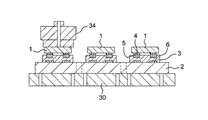
図18は、回路基板102の上面に接合材料(熱硬化性樹脂材料)の一例である樹脂シート103を介して配置(仮止め)された半導体素子101を、加圧ツール110にて加圧しながら実装を行う状態を示す図である。図18に示すように、回路基板102は、ステージ115により保持され、ステージ115には、樹脂シート103を熱硬化させるための加熱を行う加熱ヒータ116が内蔵されている。また、加圧ツール110は、その下面である加圧面に凹部111が形成されたツール本体部112と、この凹部111内に配置されたゴム材料により形成された弾性体113とを備えている。また、半導体素子101の図示下面であるアクティブ面には、複数のアルミ電極(素子電極)104が形成されており、各々のアルミ電極104には、バンプ(突起電極)105が形成されている。また、回路基板102における半導体素子101の実装位置には、アルミ電極114及びバンプ115に対応するように基板電極106が形成されている。
FIG. 18 shows a state in which a
このような構成を有する従来の実装装置において、まず、ステージ115の上面に回路基板102を配置して保持する。回路基板102におけるそれぞれの実装位置には、予め樹脂シート103を介して半導体素子101が配置(仮止め)されている。次に、回路基板102上に配置された1個の半導体素子101と、加圧ツール110との位置合わせを行う。その後、加圧ツール110を下降させて、弾性体113を介して半導体素子101及び樹脂シート103を押圧して、半導体素子101のそれぞれのアルミ電極104を、バンプ105を介してそれぞれの基板電極106に接続するとともに、この接続箇所の周囲が樹脂シート103により覆われた状態とする。それとともに、ステージ115の加熱ヒータ116により回路基板102を加熱することで、樹脂シート103を加熱して熱硬化させる。その結果、半導体素子101と回路基板102とが電気的に接続されるとともに、この状態において、接続部分を樹脂シート103にて封止し、かつ、半導体素子101と回路基板102とを接着して、回路基板102に半導体素子101が実装される。このように弾性体113を用いて加圧することにより、加圧された樹脂シート103が半導体素子101の周囲に拡がって形成されるフィレット部に対しても、弾性体113の変形により加圧することができ、十分な加圧力を付加して、実装信頼性を向上させることができる。
In the conventional mounting apparatus having such a configuration, first, the
しかしながら、従来の実装方法では、樹脂シート103にフィレット部に、適切な加圧力を付加するために弾性体113を介して加圧する加圧ツール110の構造が採用されていることにより、半導体チップ101の実装姿勢における平行度が保てない場合が生じるという問題がある。例えば、回路基板102に樹脂シート103を介して仮止めされた状態において、半導体素子101と回路基板102との間の平行度が維持されていないような場合にあっては、その後、加圧ツール110により半導体素子101を加圧する際に、軟らかい弾性体113により半導体素子101を加圧することになるため、傾いて仮止めされた半導体素子101に対して、横方向に力が加わり、半導体素子101の実装位置に位置ズレが生じる場合がある。このような場合にあっては、実装信頼性も低下することになる。
However, the conventional mounting method employs the structure of the pressurizing
従って、本発明の目的は、上記問題を解決することにあって、基板上に熱硬化性樹脂材料を介して配置された半導体素子を、加熱加圧ツールにて押圧して基板に実装する半導体素子の実装において、半導体素子と基板との間の平行度を確実に保ちながら、実装信頼性を向上させることができる半導体素子の実装装置および実装方法を提供することにある。 Accordingly, an object of the present invention is to solve the above-described problem, and a semiconductor device which is mounted on a substrate by pressing a semiconductor element disposed on the substrate via a thermosetting resin material with a heating and pressing tool. An object of the present invention is to provide a semiconductor device mounting apparatus and a mounting method capable of improving mounting reliability while reliably maintaining parallelism between a semiconductor device and a substrate.
上記目的を達成するために、本発明は以下のように構成する。 In order to achieve the above object, the present invention is configured as follows.
本発明の第1態様によれば、基板上に熱硬化性樹脂材料を介して配置された半導体素子を、加熱加圧ツールにて押圧して実装する半導体素子実装装置において、
シート部材を水平に張架して保持するシート保持部と、
上記張架された状態の上記シート部材で、上記半導体素子の上面を加圧するように、上記シート保持部を下降させる保持部昇降装置と、
その加圧面に配置されたエラストマーと、上記エラストマーを加熱する加熱部とを備える加熱加圧ツールと、
上記シート部材を介して上記エラストマーにて上記半導体素子の上面を加圧するとともに、上記エラストマーを介して上記半導体素子及び上記樹脂材料を加熱するように、上記加熱加圧ツールを下降させるツール昇降装置とを備え、
上記加熱加圧ツールは、上記エラストマーがその内側に配置される凹部を、上記加圧面に有する剛体部を備え、
上記エラストマーは、上記剛体部の上記凹部の中央に配置される第1のエラストマーと、上記凹部において上記第1のエラストマーの周囲に配置される第2のエラストマーとを備え、上記第1のエラストマーは上記第2のエラストマーよりも高い硬度を有する、半導体素子実装装置を提供する。
本発明の第2態様によれば、上記半導体素子は、突起電極数が100〜1000である、第1態様に記載の半導体素子実装装置を提供する。
本発明の第3態様によれば、上記シート部材が樹脂シートである、第1態様または第2態様に記載の半導体素子実装装置を提供する。
本発明の第4態様によれば、上記シート部材を介して、上記エラストマーにて、上記半導体素子の上面および側面ならびに上記樹脂材料を押圧する、第1態様から第3態様のいずれか1つに記載の半導体素子実装装置を提供する。
本発明の第5態様によれば、上記シート部材の弾性率は、上記エラストマーの弾性率より低い、第1態様から第4態様のいずれか1つに記載の半導体素子実装装置を提供する。
According to the first aspect of the present invention, in a semiconductor element mounting apparatus for mounting a semiconductor element disposed on a substrate via a thermosetting resin material by pressing with a heating and pressing tool,
A sheet holding unit for holding the sheet member horizontally stretched;
A holding unit lifting device for lowering the sheet holding unit so as to pressurize the upper surface of the semiconductor element with the sheet member in the stretched state;
A heating and pressing tool comprising an elastomer disposed on the pressing surface and a heating unit for heating the elastomer;
A tool lifting and lowering device that pressurizes the upper surface of the semiconductor element with the elastomer through the sheet member and lowers the heating and pressing tool so as to heat the semiconductor element and the resin material through the elastomer; equipped with a,
The heating and pressurizing tool includes a rigid body portion having a concave portion in which the elastomer is disposed on the inner side thereof on the pressing surface,
The elastomer includes a first elastomer disposed in the center of the concave portion of the rigid body portion, and a second elastomer disposed around the first elastomer in the concave portion, wherein the first elastomer is Provided is a semiconductor device mounting apparatus having a hardness higher than that of the second elastomer .
According to a second aspect of the present invention, there is provided the semiconductor element mounting apparatus according to the first aspect, wherein the number of protruding electrodes is 100 to 1000.
According to a third aspect of the present invention, there is provided the semiconductor element mounting apparatus according to the first aspect or the second aspect , wherein the sheet member is a resin sheet.
According to the fourth aspect of the present invention, in any one of the first to third aspects, the upper surface and the side surface of the semiconductor element and the resin material are pressed with the elastomer through the sheet member. The semiconductor element mounting apparatus described is provided.
According to a fifth aspect of the present invention, there is provided the semiconductor element mounting apparatus according to any one of the first to fourth aspects, wherein the elastic modulus of the sheet member is lower than the elastic modulus of the elastomer.
本発明の第6態様によれば、上記第1のエラストマーは、上記第2のエラストマーよりも高い熱伝導性を有する、第1態様から第5態様のいずれか1つに記載の半導体素子実装装置を提供する。
According to a sixth aspect of the present invention, in the semiconductor element mounting apparatus according to any one of the first to fifth aspects , the first elastomer has higher thermal conductivity than the second elastomer. I will provide a.
本発明の第7態様によれば、上記加熱加圧ツールによる上記半導体素子の加熱加圧状態において、上記第1のエラストマーが上記半導体素子に上面を、上記シート部材を介して加圧するように配置され、上記第2のエラストマーが、上記半導体素子の周囲へ拡がるように配置される上記樹脂材料を、上記シート部材を介して加圧するように配置される、第1態様から第6態様のいずれか1つに記載の半導体素子実装装置を提供する。
According to the seventh aspect of the present invention, the first elastomer is arranged so that the upper surface of the semiconductor element is pressed onto the semiconductor element through the sheet member in the heating and pressing state of the semiconductor element by the heating and pressing tool. Any one of the first to sixth aspects, wherein the second elastomer is arranged to pressurize the resin material arranged so as to spread around the semiconductor element through the sheet member . A semiconductor element mounting apparatus as described in one is provided.
本発明の第8態様によれば、上記剛体部における上記凹部の縁部が、上記加熱加圧ツールの加圧高さ位置を上記基板表面との当接により規制する加圧位置規制部である、第1態様から第7態様のいずれか1つに記載の半導体素子実装装置を提供する。
According to the eighth aspect of the present invention, the edge portion of the concave portion in the rigid body portion is a pressurizing position restricting portion that restricts the pressurizing height position of the heating and pressurizing tool by contact with the substrate surface. A semiconductor element mounting apparatus according to any one of the first to seventh aspects is provided.
本発明によれば、熱硬化性樹脂材料を介して基板上に配置された半導体素子を、まず、水平に張架されたシート部材を介して加圧することにより、基板に対する半導体素子の平行度を矯正した後、エラストマーを介して加熱加圧ヘッドにより加圧して、半導体素子の上面だけでなく、その周囲に拡がる熱硬化性樹脂をも加圧することができる。従って、基板に対する半導体素子の平行度を保って、実装位置の精度を確保することができるとともに、熱硬化性樹脂に対しても適切な荷重を付加して確実な封止及び接着を行うことができる。よって、半導体素子の実装において、実装の信頼性を向上させることができる。 According to the present invention, a semiconductor element placed on a substrate via a thermosetting resin material is first pressed through a sheet member that is horizontally stretched, whereby the parallelism of the semiconductor element with respect to the substrate is increased. After the correction, it is possible to pressurize not only the upper surface of the semiconductor element but also the thermosetting resin spreading around the upper surface of the semiconductor element by pressing with a heating and pressing head through the elastomer. Accordingly, the parallelism of the semiconductor element with respect to the substrate can be maintained to ensure the accuracy of the mounting position, and an appropriate load can be applied to the thermosetting resin to perform reliable sealing and adhesion. it can. Therefore, the mounting reliability can be improved in the mounting of the semiconductor element.
以下に、本発明にかかる実施の形態を図面に基づいて詳細に説明する。 Embodiments according to the present invention will be described below in detail with reference to the drawings.
本発明の一の実施形態にかかる半導体素子の実装装置9の構成を示す模式断面図を図1A及び図1Bに示す。なお、図1Aは、図1Bの実装装置9におけるA−A’線の断面図である。また、本実施形態の半導体素子の実装装置9は、回路基板2に仮止め(配置)された状態の半導体素子1を回路基板2との間で電気的に導通させるとともに、機械的に固定するために、半導体素子1を加熱及び加圧する装置である。
1A and 1B are schematic cross-sectional views showing the configuration of a semiconductor
図1A及び図1Bに示すように、実装装置9は、回路基板2をその下面側から支持するとともに、その支持位置を解除可能に保持するステージ15と、ステージ15に保持された状態の回路基板2上に仮止めされた半導体素子1に対して、実装のための加熱および加圧を行う加熱加圧ツール10と、加熱加圧ツール10による半導体素子1の加圧の前に、仮止め状態の半導体素子1の回路基板2に対する平行度を矯正する平行度矯正装置20とを備えている。
As shown in FIG. 1A and FIG. 1B, the mounting
まず、ステージ15は、剛体材料にて構成され、その上面である回路基板2の保持面が平坦に形成されている。また、この保持面には、配置された回路基板2を真空吸引することで吸着保持する複数の吸着孔16が形成されている。回路基板2における上面には、半導体素子1の複数の実装位置が配置されており、各々の実装位置には、複数の基板電極6が形成されている。また、半導体素子1の下面であるアクティブ面には、複数のアルミ電極4が形成されており、各々のアルミ電極4にはバンプ5が形成されている。なお、それぞれの基板電極6は、アルミ電極4との配置と対応するように形成されている。また、図1Aに示す状態においては、回路基板2のそれぞれの実装位置に、半導体素子1が熱硬化性樹脂材料である樹脂シート(例えば、異方性導電性樹脂フィルムあるいは絶縁性樹脂フィルム)3を介して配置された状態、すなわち仮止めされた状態にて配置されている。なお、本実施形態において、「仮止め状態」とは、半導体素子1の配置位置が完全に固定されておらず、外力を付加することで、その配置位置が容易に変化するような状態のことである。
First, the
加熱加圧ツール10は、剛体材料にて形成されたツール本体部12(剛体部)と、このツール本体部12の図示下面に形成された略直方体形状の凹部11を埋めるように取り付けられた弾性体であるエラストマー13と、ツール本体部12に内蔵された加熱ヒータ14(加熱部)とを備えている。また、加熱加圧ツール10には、ツール本体部12とエラストマー13とを一体的に昇降させるツール昇降装置17が備えられている。加熱ヒータ14は、半導体素子1の実装処理を行う間は、例えば、常時200℃〜300℃に加熱されている。そのため、ツール本体部12の凹部11に取り付けられているエラストマー13もツール本体部12からの伝熱で常時180℃〜280℃に加熱されている。また、エラストマー13は、このように280℃の加熱状態でも弾力性を持つシリコーン樹脂で形成され、さらにゴム硬度として40以上80以下の仕様のものが用いられる。また、ツール本体部12の凹部11の縁部18(加圧位置規制部)は、下降状態において、回路基板2の表面との当接部となっており、この縁部18が回路基板2と当接されることで、ツール昇降装置17による加熱加圧ツール10の下降位置が規制される。また、この下降位置の規制位置(加熱加圧処理位置)において、半導体素子1に対する加熱加圧処理が行われる。さらに、凹部11の深さは、少なくとも、半導体素子1の実装高さ(実装後の上面の高さ)よりも大きく設定されている。
The heating and
平行度矯正装置20は、シート部材の一例である保護テープ21を、ステージ15の保持面に対して水平な状態にて張架して保持するホルダ22(シート保持部)を備えている。ホルダ22は、供給軸23に巻き取られた状態の保護テープ21をその一端にて供給可能に支持するとともに、供給された保護テープ21をその他端にて巻き取り可能に回収軸24にて巻き取って支持する。供給軸23と回収軸24とは、ホルダ22にて同じ高さ位置に取り付けられており、その結果、供給軸23と回収軸24との間で保護テープ21が所定の張力が付与された状態にて水平に張架されている。この保護テープ21は、加熱加圧ツール10の表面を、半導体素子1や樹脂シート3と直接接触することを防止する機能を有する。例えば、保護テープ21は30μm厚のフッ化樹脂フィルムで、弾性率は392MPaのものが使用される。なお、保護テープ21は、半導体素子1及びその周囲に拡がって配置される樹脂シート3を十分に覆うことができるような幅寸法に形成されている。また、保護テープ21を支持する供給軸23と回収軸24とを同期させて回動させる図示しない回動手段が備えられている。
The
平行度矯正装置20には、支持する保護テープ21とともにホルダ22を一体的に昇降させるホルダ昇降装置26が備えられている。ホルダ22は、剛体材料にて形成され、その中央には、加熱加圧ツール10が接触することなく通過可能な開口部25が形成されている。従って、加熱加圧ツール10の昇降が、ホルダ22により妨げられることがない。また、このホルダ22には、下降した状態で回路基板2をステージ15に対して押さえる基板当接部22aがその外周下端に設けられている。なお、この外周下端の基板当接部22aは、加熱加圧ツール10よりも外側に位置されるようにその配置が決定されている。
The
次に、このような構成の実装装置9を用いて、回路基板2に半導体素子1を実装する手順について、図2〜図9の模式断面図を用いて、その前工程をも含めて説明する。
Next, a procedure for mounting the
まず、図2〜図4は、実装装置9に設置する前の回路基板2の作成工程を示している。図2に示すように、作業台30上に保持された回路基板2の上に、所定の長さにカットされた樹脂シート3を貼り付ける。具体的には、ベーステープ31に貼られた樹脂シート3に所定の間隔でカット部32を形成した後、加熱加圧ツール33(加熱加圧ツール10とは別のツール)を用いて、回路基板2におけるそれぞれの半導体素子1の実装領域のみにベーステープ31の上から押圧する。この時の加熱加圧ツール33の加熱温度は、樹脂シート3が硬化反応を起こさず、かつ、樹脂シート3の軟化を起こさせ回路基板2への貼り付けを容易にする温度に設定されており、例えば、加熱温度60〜100℃、加圧時間0.1〜1秒の加熱加圧処理が行われて、樹脂シート3の回路基板2への貼り付けを行う。
First, FIGS. 2 to 4 show a process of creating the
次に、図3に示すように、それぞれの実装領域に樹脂シート3が貼り付けられた回路基板2を作業台30に吸着保持させて平坦にした状態で、樹脂シート3を介して半導体素子1を仮止めする。具体的には、吸着ツール34で半導体素子1を真空吸着し、回路基板2の実装領域と位置合わせを行った後、基板電極6と、半導体素子1のバンプ5とが樹脂シート3を介して対向し、かつ半導体素子1が樹脂シート3により保持されるように、荷重1〜3kgf程度かつ±5μm以下の位置精度で半導体素子1を回路基板2に仮止めする。なお、バンプ5としては、ワイヤボンディング工法を応用したスタッドバンプ、またはウェットメッキ処理で形成するメッキバンプを用いる。
Next, as shown in FIG. 3, in a state where the
次に、図4に示すように、作業台30の吸着保持を解除し、それぞれの実装領域に樹脂シート3を介して半導体素子1が仮止めされた状態の回路基板2を作業台30から取り外す。このように作業台30から取り外された状態にてそのフレキシブル性などにより回路基板2は変形し、例えば、図示中央の半導体素子1のように仮止め姿勢が変化する、すなわち、回路基板2に対する半導体素子1の平行度にズレが生じるような場合がある。また、そのフレキシブル性などにより回路基板2自身の反りが原因で、このような仮止め姿勢が変化する場合がある。
Next, as shown in FIG. 4, the suction holding of the work table 30 is released, and the
このように一部半導体素子1においてその仮止め姿勢が変化した状態の回路基板2を、図1Aのステージ15に乗せ換えた直後の状態を、図5に示す。図5に示す状態においては、ホルダ22と加熱加圧ツール10は共に回路基板2の表面から離間された上昇位置に配置されている。なお、図5〜図9は、実装装置9における実装工程を示す模式図である。
FIG. 5 shows a state immediately after the
次に、図6に示すように、実装装置9において、ホルダ昇降装置26によりホルダ22の下降を開始する。なお、この下降開始の際には、図5に示すように、ホルダ22において供給軸23と回収軸24との間で保護テープ21が張架された状態とされている。ホルダ22が下降されると、所定の張力にて張架された状態の保護テープ21の下面が、半導体素子1の背面に当接し、さらにホルダ22が降下することによって、その仮止め姿勢が変化した半導体素子1に保護テープ21から下向きの加圧力が作用する。この下向きの加圧力が作用することにより、水平に張架された状態の保護テープ21に倣うようにして、仮止め状態の半導体素子1の傾いた姿勢が、回路基板2に対して略水平な状態へと矯正される。なお、ここでは保護テープ21の弾性が有効に作用して、様々な傾き姿勢を有する半導体素子1の仮止め姿勢を矯正することができる。特に、保護テープ21の弾性は、エラストマー13に比して十分に低いものであるため、仮止め状態の半導体素子1の水平方向に位置ズレを生じさせることなく、その姿勢、すなわち平行度を矯正することができる。
Next, as shown in FIG. 6, in the mounting
このように、半導体素子1の平行度の矯正が行われた後、さらにホルダ22を下降させると、図7に示すように、ホルダ22の下端部である基板当接部22aが、保護シート21を介して回路基板2の表面に当接する。この基板当接部22aの回路基板2への当接により、回路基板2に下向きの力が作用され、反り状態にあった回路基板2の反りが矯正され、ステージ15に回路基板2が密着される。このような状態において、例えば、ステージ15の吸着孔16により回路基板2を吸着保持することにより、回路基板2を水平な状態かつ半導体素子1が回路基板2に対して平行な状態にて、回路基板2のステージ15による保持が行われる。また、このような状態においてはホルダ22の基板当接部22aにより回路基板2がステージ15に対して押し付けられて保持された状態とされている。なお、本実施形態においては、ステージ15が吸着孔16による吸着機能を有する場合について説明するが、このような場合に代えて、ステージ15が吸着機能を有さないような場合であっても、ホルダ22による回路基板2の保持機能を用いて、回路基板2の保持を行うことができる。
As described above, when the parallelism of the
このように、ステージ15と半導体素子1を平行な状態とさせることで、次に説明する加熱加圧ツール10による加熱加圧工程において、軟らかい弾性体であるエラストマー13により半導体素子1を押圧した時に、半導体素子1に対して横方向への力が作用し、位置ズレ不良となることを確実に防止することができる。
In this way, when the
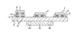
次に、図8に示すように、ホルダ22で回路基板2に下方の力を加え、回路基板2の反りを矯正した状態のまま、ツール昇降装置17による加熱加圧ツール10の下降を開始する。加熱加圧ツール10は、ホルダ22の中央に設けられた開口部を通過して下降され、保護テープ21を介して、凹部11の縁部18が回路基板2の表面に接触することで、その下降位置が規制された状態とされる。このような状態において、加熱加圧ツール10の凹部11に設けられたエラストマー13が、保護テープ21を介して、半導体素子1の上面に接触し、その後エラストマー13が弾性変形されることにより、半導体素子1に押圧力を付与し、それぞれのバンプ5が回路基板2の基板電極6に接触され、押圧により変形されてその接触面積が増加された状態にて電気的接続がなされる。また、このような押圧により、樹脂シート3は周囲に拡がるように押圧されることになるが、弾性変形されたエラストマー13により、保護テープ21を介して半導体素子1の側部とともに、押し拡げられた樹脂シート3の外周部全体が押圧される。さらに、このような押圧状態において、ツール本体部12に内蔵された加熱ヒータ14より、エラストマー13を介して伝熱が行われ、樹脂シート3が加熱温度180〜200℃、加熱加圧時間10〜20秒にて加熱加圧が行われ、樹脂シート3が熱硬化される。
Next, as shown in FIG. 8, a downward force is applied to the
その結果、図9に示すように、半導体素子1のバンプ5と回路基板2の基板電極6とが電気的に接続された状態とされるとともに、この接続状態が熱硬化された樹脂シート3により封止された状態にて、半導体素子1が回路基板2に固定、すなわち実装される。また、半導体素子1の周囲にはみ出した樹脂シート3は、エラストマー13により包み込まれるように加圧されるため、はみ出た樹脂シート3の周部は、山のすそ野のようななだらかな円弧状のフィレット部Fとして形成される。このような形状のフィレット部Fが形成されることにより、例えば、エラストマー13を用いない加圧方法と比して、樹脂材料のはみ出し量が少なくなるとともに、半導体素子1の4辺で略同一形状のフィレット部Fを形成することができるため、バラツキのすくない形状を形成することができる。なお、下降状態にあったホルダ22と加熱加圧ツール10は、その後上昇されて、半導体素子1の回路基板2への実装処理が完了する。
As a result, as shown in FIG. 9, the
エラストマー13は、ゴム硬度40〜80と例えば消しゴムや自動車用のタイヤに近い軟らかさを有しており、直方体である半導体素子1を押圧した時に、半導体素子1のエッジ部分を押しているエラストマー13に大きな応力がかかる場合がある。複数回の加圧処理を繰り返すと、このようなエッジ部分に接触する部分におけるエラストマー13に割れ等が生じる場合が考えられる。しかしながら、本実施形態においては、保護テープ21を介してエラストマー13による半導体素子1の加圧を行っているため、半導体素子1のエッジ部分からエラストマー13に付加される局所応力を保護テープ21により緩和させることができ、このような割れの発生を未然に防止することができる。さらに、保護テープ21を加熱加圧処理毎に巻き取り、新たな保護テープ21を供給して張架させることにより、半導体素子1およびエラストマー13に触れる部分の保護テープ21は、毎回新たなものとすることができるため、半導体素子1に付着したホコリ、ゴミ、汚れなどの異物が、保護シート15に転写しても、次の半導体素子1が汚染されることはない。また、エラストマー13にほこり、ゴミ、汚れが付着することも防止され、エラストマー13の寿命を長くすることができる。
The
また、加熱加圧ツール10の下降は特別な荷重制御や位置制御を必要とせず、単純な上下駆動だけで構成されている。すなわち、加熱加圧ツール10の下降位置は、ツール本体部12の凹部11の縁部18が保護テープ21を介して回路基板2と当接することにより規制される構成が採用されている。このような構成が採用されていることにより、上記従来の実装装置に比べて、複雑な下降位置の制御が、保護テープ21の厚みや弾性力に応じて軽減され、装置構成の簡素化を図ることが可能となる。また、保護テープ21を介して縁部18が回路基板2と当接するので、縁部18が当接することによる回路基板2の損傷を抑えることができる。なお、半導体素子1への加圧力は、加熱加圧ツール10の凹部11の深さ寸法と、エラストマー13のヤング率などの物性と、半導体素子1の寸法から決定される。
Further, the lowering of the heating and
また、半導体素子1をエラストマー13で包み込むように加圧しているため、樹脂シート3に対しても包み込むようにその周囲から圧力がかかるため、樹脂シート3内部に混入していた気泡を小さくすることができ、エラストマー13を用いない場合と比してボイドの形成を抑制することができる。
Further, since the
半導体素子1は、例えば2mm角〜12mm角、加熱加圧ツール10の加圧面は例えば、6mm角〜16mm角、エラストマー13の大きさは4mm〜14mm角、その厚みは5mm〜15mmで構成することができる。
The
また、エラストマー13は、軟らかい弾性力と高熱伝導の特性を求められるため、均質なゴム材料を用いることが好ましく、半導体素子1の熱容量が大きい場合は、ゴム材料の中に熱伝導の高い、カーボン、金、銅など高熱伝導材料を含浸させた高熱伝導性ゴムを使用することが好ましい。
In addition, since the
さらに、図8から明らかなように、加熱加圧ツール10が半導体素子1を押圧している10〜20秒間の状態に注目すると、隣接する実装部品としての半導体素子1と加熱加圧ツール10との間には、ホルダ22の基板当接部22a、ホルダ22自体、保護テープ21が介在して、加熱加圧ツール10からの熱輻射を遮蔽している。このように加熱加圧ツール10から隣接する半導体素子1への熱輻射を遮ることによって、高密度実装の場合であってもその実装品質を高い状態にて保つことができる。また、ステージ15からの熱伝導を抑えるために、本実施形態では、ステージ15として1つの半導体素子1のサイズよりも僅かに大きい程度の大きさとなるように小型化されたステージ15を採用している。このような2つの効果により、実装処理が未完の半導体素子1における樹脂シート3の熱硬化反応が発生せず、その良好な実装品質を得ることができる。具体的には、熱遮蔽部を設けなかった場合には、図8の実装工程を実施した場合には、隣接する半導体素子1の温度が80〜100℃に上昇するが、このような熱遮蔽部を設けることによって40〜60℃に抑制することができる。
Further, as apparent from FIG. 8, when attention is paid to the state of the heating and
なお、保護テープ21は、単数または複数の半導体素子の実装が完了するたびに、回収軸24に巻き取られて、供給軸23から新たな保護テープ21が供給される。
The
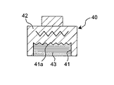
ここで、本実施形態の実装装置が備える加熱加圧ツールの変形例について説明する。 Here, a modified example of the heating and pressing tool provided in the mounting apparatus of the present embodiment will be described.
図10に示す加熱加圧ツール40は、ツール本体部42の凹部41の底面に凹凸部41aを形成し、ツール本体部42とエラストマー43との接触面積を増大させ、伝熱の効果を高めている。このような構成を採用することにより、半導体装置1の圧着時におけるエラストマー43の低下温度を、凹凸部41aが形成されていない場合の20℃から10℃へと低減することができる。
The heating and
図11に示す加熱加圧ツール50は、凹部11に設置されるエラストマー53を第1のエラストマー53aと第2のエラストマー53bの2層構造としたものである。具体的には、図12に示すように、半導体素子1を押圧する部分、すなわち凹部11の中央部には、ゴム硬度50〜80と比較的硬い第1のエラストマー53aを配置し、半導体素子1の周囲のはみ出した樹脂シート3を押圧する部分、すなわち凹部11の周部には、ゴム硬度20〜49と比較的軟らかいエラストマー53bを配置している。このように2種類の硬度のエラストマーを用いることにより、中央部の第1のエラストマー53aにより半導体素子1に対して比較的強い加圧力を付加することができ、周部の第2のエラストマー53bにより樹脂シート3に対して適切な加圧力を与えることができる。このような構成は、例えば、半導体素子1の突起電極数が100〜1000バンプと多く、半導体素子1に対して十分な加圧力を付加する必要があるような場合に有効である。
In the heating and
逆に、図13及び図14に示すように、半導体素子1の突起電極が1〜99と比較的少ない場合には、2層構造のエラストマーを逆の配置とすることが好ましい。具体的には、加熱加圧ツール60において、半導体素子1を押圧する部分には、ゴム硬度20〜49と比較的軟らかい第1のエラストマー63aを配置し、半導体素子1の周囲のはみ出した樹脂シート3を押圧する部分には、ゴム硬度50〜80と比較的硬い第2のエラストマー63bを配置することが好ましい。半導体素子1の突起電極が比較的少ない場合には、1つあたりの突起電極にかかる加熱加圧ツール60の加圧力が大きくなり過ぎて、半導体素子1に損傷などが発生する恐れがある。上記のように第1及び第2のエラストマー63a,63bを配置することにより、半導体素子1を比較的低い荷重でエラストマー63aの内側に埋め込みながら、樹脂シート3に対して適切な荷重を付加することができる。したがって、1つあたりの突起電極にかかる加熱加圧ツール60の加圧力を適切な大きさに抑えて、半導体素子1の損傷などの発生を抑えることができる。なお、エラストマーの硬度は、半導体素子1への荷重と、周部への荷重とのバランスで決定すればよい。
On the contrary, as shown in FIGS. 13 and 14, when the number of protruding electrodes of the
また、半導体素子1の厚みが厚い場合には、図15に示す上下方向2層のエラストマーが有効である。つまり、図15に示す加熱加圧ツール70のように、第1及び第2のエラストマー73a、73bを上下方向に2層構造として、下層にゴム硬度20〜49と比較的軟らかい第2のエラストマー73bを配置し、上層にゴム硬度50〜80と比較的硬い第1のエラストマー73aを配置することにより、半導体素子1に対して均一に下方への加圧力を与えながら、半導体素子1の周囲を低い圧力で包み込みながら、樹脂シート3に対して適切な荷重を付加することができる。つまり、半導体素子1の厚みが厚い場合には、上記エラストマーを2層構造とすることにより、自然とその背面に高い荷重がかかり、かつ、周部には低い荷重がかかることになり、樹脂シート3に対して適切な荷重を付加することができる。
Further, when the
また、図16に示す加熱加圧ツール80のように、ツール本体部82の凹部81の底部中央部分に突出部81aを形成して、エラストマー83の中央部分より半導体素子1に対して付加される押圧力をその周部よりも高めるような構成を採用することもできる。
Further, like the heating and
さらに、図17に示す加熱加圧ツール90のように、縦方向の2層構造と、横方向の2層構造とを組み合わせて、凹部11の底部中央部分に比較的硬い第1のエラストマー93aを配置し、この第1のエラストマー93aを包み込むように比較的軟らかい第2のエラストマー93bを配置するような構成を採用することができる。
Further, as in the heating and
また、上記それぞれの2層構造において、中央に配置されるエラストマーとして高熱伝導性を有するものを選択することにより、熱が伝達され難い樹脂シート3の中央部に確実に熱を伝達することができ、確実な熱硬化を行うことができる。
Further, in each of the above two-layer structures, by selecting an elastomer having high thermal conductivity as the elastomer disposed in the center, heat can be reliably transmitted to the central portion of the
なお、上記の実施形態では基板の具体例が回路基板2の場合を例に挙げて説明したが、このような場合に代えて、弾性を有する多層構造のフレキシブル基板が採用されるような場合にも同様に本実施形態を適用することができる。
In the above embodiment, the case where the specific example of the substrate is the
なお、上記様々な実施形態のうちの任意の実施形態を適宜組み合わせることにより、それぞれの有する効果を奏するようにすることができる。 It is to be noted that, by appropriately combining arbitrary embodiments of the various embodiments described above, the effects possessed by them can be produced.
本発明は、例えば、薄く反り易い樹脂材料で形成された回路基板に、複数の半導体素子をフリップチップ実装する際に、基板の反りと半導体素子の傾き(平行度)を矯正して、良好な接合品質を得ることができ、小型軽量化が要求される携帯電話装置やデジタルカメラなどの製品に使用される半導体パッケージの実装に有効である。 For example, when a plurality of semiconductor elements are flip-chip mounted on a circuit board formed of a thin and easily warped resin material, the present invention corrects the warpage of the substrate and the inclination (parallelism) of the semiconductor elements, Bonding quality can be obtained, and it is effective for mounting semiconductor packages used in products such as mobile phone devices and digital cameras that require a reduction in size and weight.
1 半導体素子
2 回路基板
3 樹脂シート
4 アルミ電極
5 バンプ
6 基板電極
9 実装装置
10 加熱加圧ツール
11 凹部
12 ツール本体部
13 エラストマー
14 加熱ヒータ
15 ステージ
20 平行度矯正装置
21 保護テープ
22 ホルダ
DESCRIPTION OF
Claims (8)
シート部材を水平に張架して保持するシート保持部と、
上記張架された状態の上記シート部材で、上記半導体素子の上面を加圧するように、上記シート保持部を下降させる保持部昇降装置と、
その加圧面に配置されたエラストマーと、上記エラストマーを加熱する加熱部とを備える加熱加圧ツールと、
上記シート部材を介して上記エラストマーにて上記半導体素子の上面を加圧するとともに、上記エラストマーを介して上記半導体素子及び上記樹脂材料を加熱するように、上記加熱加圧ツールを下降させるツール昇降装置とを備え、
上記加熱加圧ツールは、上記エラストマーがその内側に配置される凹部を、上記加圧面に有する剛体部を備え、
上記エラストマーは、上記剛体部の上記凹部の中央に配置される第1のエラストマーと、上記凹部において上記第1のエラストマーの周囲に配置される第2のエラストマーとを備え、上記第1のエラストマーは上記第2のエラストマーよりも高い硬度を有する、半導体素子実装装置。 In a semiconductor element mounting apparatus for mounting a semiconductor element disposed on a substrate via a thermosetting resin material by pressing with a heating and pressing tool,
A sheet holding unit for holding the sheet member horizontally stretched;
A holding unit lifting device for lowering the sheet holding unit so as to pressurize the upper surface of the semiconductor element with the sheet member in the stretched state;
A heating and pressing tool comprising an elastomer disposed on the pressing surface and a heating unit for heating the elastomer;
A tool lifting and lowering device that pressurizes the upper surface of the semiconductor element with the elastomer through the sheet member and lowers the heating and pressing tool so as to heat the semiconductor element and the resin material through the elastomer; equipped with a,
The heating and pressurizing tool includes a rigid body portion having a concave portion in which the elastomer is disposed on the inner side thereof on the pressing surface,
The elastomer includes a first elastomer disposed in the center of the concave portion of the rigid body portion, and a second elastomer disposed around the first elastomer in the concave portion, wherein the first elastomer is A semiconductor element mounting apparatus having a hardness higher than that of the second elastomer .
Priority Applications (1)
| Application Number | Priority Date | Filing Date | Title |
|---|---|---|---|
| JP2007176209A JP5122192B2 (en) | 2007-07-04 | 2007-07-04 | Semiconductor device mounting equipment |
Applications Claiming Priority (1)
| Application Number | Priority Date | Filing Date | Title |
|---|---|---|---|
| JP2007176209A JP5122192B2 (en) | 2007-07-04 | 2007-07-04 | Semiconductor device mounting equipment |
Publications (3)
| Publication Number | Publication Date |
|---|---|
| JP2009016544A JP2009016544A (en) | 2009-01-22 |
| JP2009016544A5 JP2009016544A5 (en) | 2010-08-05 |
| JP5122192B2 true JP5122192B2 (en) | 2013-01-16 |
Family
ID=40357101
Family Applications (1)
| Application Number | Title | Priority Date | Filing Date |
|---|---|---|---|
| JP2007176209A Expired - Fee Related JP5122192B2 (en) | 2007-07-04 | 2007-07-04 | Semiconductor device mounting equipment |
Country Status (1)
| Country | Link |
|---|---|
| JP (1) | JP5122192B2 (en) |
Families Citing this family (6)
| Publication number | Priority date | Publication date | Assignee | Title |
|---|---|---|---|---|
| JP5208205B2 (en) * | 2008-04-18 | 2013-06-12 | パナソニック株式会社 | Flip chip mounting method, flip chip mounting apparatus, and tool protection sheet used therefor |
| JP6043058B2 (en) * | 2011-11-07 | 2016-12-14 | デクセリアルズ株式会社 | Connection device, method for manufacturing connection structure, method for manufacturing chip stack component, and method for mounting electronic component |
| KR101345037B1 (en) * | 2012-08-23 | 2013-12-26 | 앰코 테크놀로지 코리아 주식회사 | Manufacture apparatus for semiconductor device and manufacturing method the same |
| WO2016031806A1 (en) * | 2014-08-25 | 2016-03-03 | 東レエンジニアリング株式会社 | Mounting head and mounting device in which same is used |
| WO2022013995A1 (en) * | 2020-07-16 | 2022-01-20 | 株式会社新川 | Mounting device |
| US11676937B2 (en) | 2021-05-04 | 2023-06-13 | Asmpt Singapore Pte. Ltd. | Flexible sinter tool for bonding semiconductor devices |
Family Cites Families (5)
| Publication number | Priority date | Publication date | Assignee | Title |
|---|---|---|---|---|
| JP4684502B2 (en) * | 2001-09-27 | 2011-05-18 | 日東電工株式会社 | Conductive connection method and release sheet used therefor |
| JP2003258413A (en) * | 2002-03-06 | 2003-09-12 | Nikkiso Co Ltd | Circuit element mounting device and method therefor |
| JP3921459B2 (en) * | 2003-07-11 | 2007-05-30 | ソニーケミカル&インフォメーションデバイス株式会社 | Mounting method and mounting apparatus for electrical parts |
| WO2006082744A1 (en) * | 2005-02-02 | 2006-08-10 | Sony Chemical & Information Device Corporation | Electric component mounting apparatus |
| JP4619209B2 (en) * | 2005-06-28 | 2011-01-26 | パナソニック株式会社 | Semiconductor element mounting method and semiconductor element mounting apparatus |
-
2007
- 2007-07-04 JP JP2007176209A patent/JP5122192B2/en not_active Expired - Fee Related
Also Published As
| Publication number | Publication date |
|---|---|
| JP2009016544A (en) | 2009-01-22 |
Similar Documents
| Publication | Publication Date | Title |
|---|---|---|
| JP5084829B2 (en) | Semiconductor device mounting structure manufacturing method, semiconductor device mounting method, and pressure tool | |
| JP5122192B2 (en) | Semiconductor device mounting equipment | |
| JP5250524B2 (en) | Semiconductor device and manufacturing method thereof | |
| JP5521547B2 (en) | Semiconductor device and manufacturing method thereof | |
| TWI485764B (en) | And a manufacturing apparatus for a laminated semiconductor device | |
| JP2004281460A (en) | Reinforcing plate sticking apparatus and sticking method | |
| JP3896017B2 (en) | Semiconductor mounting body manufacturing method and semiconductor mounting body manufacturing apparatus | |
| KR20030012808A (en) | Method for fabricating semiconductor-mounting body and apparatus for fabricating semiconductor-mounting body | |
| JP4619209B2 (en) | Semiconductor element mounting method and semiconductor element mounting apparatus | |
| JP4755222B2 (en) | Manufacturing method of semiconductor device | |
| JP5104315B2 (en) | Semiconductor package, electronic component, and electronic device | |
| JP5494546B2 (en) | Manufacturing method of semiconductor device | |
| JP2006202783A (en) | Process for manufacturing semiconductor device | |
| JP5272397B2 (en) | Adhesive film application apparatus and adhesive film application method | |
| JP6036083B2 (en) | Semiconductor device and method for manufacturing the same, electronic device and method for manufacturing the same | |
| TW201511147A (en) | Semiconductor manufacturing apparatus | |
| JP5406974B2 (en) | Thermocompression bonding apparatus and electrical component mounting method | |
| JP2009032845A (en) | Thermocompression bonding device and packaging method for electrical component | |
| JP3608226B2 (en) | Semiconductor chip mounting method and semiconductor device | |
| JP5451053B2 (en) | Flip chip mounting method and flip chip mounting apparatus | |
| JPH11330010A (en) | Producing method for semiconductor device | |
| JP2011071267A (en) | Electronic device package, method of manufacturing the same, and electronic equipment | |
| JP5576528B2 (en) | Semiconductor device | |
| JP2010045104A (en) | Method for producing electronic component | |
| JP2008243998A (en) | Method of reforming curvature of printed-circuit board |
Legal Events
| Date | Code | Title | Description |
|---|---|---|---|
| A521 | Written amendment |
Free format text: JAPANESE INTERMEDIATE CODE: A523 Effective date: 20100621 |
|
| A621 | Written request for application examination |
Free format text: JAPANESE INTERMEDIATE CODE: A621 Effective date: 20100621 |
|
| A977 | Report on retrieval |
Free format text: JAPANESE INTERMEDIATE CODE: A971007 Effective date: 20111227 |
|
| A131 | Notification of reasons for refusal |
Free format text: JAPANESE INTERMEDIATE CODE: A131 Effective date: 20120117 |
|
| A521 | Written amendment |
Free format text: JAPANESE INTERMEDIATE CODE: A523 Effective date: 20120319 |
|
| TRDD | Decision of grant or rejection written | ||
| A01 | Written decision to grant a patent or to grant a registration (utility model) |
Free format text: JAPANESE INTERMEDIATE CODE: A01 Effective date: 20121002 |
|
| A01 | Written decision to grant a patent or to grant a registration (utility model) |
Free format text: JAPANESE INTERMEDIATE CODE: A01 |
|
| A61 | First payment of annual fees (during grant procedure) |
Free format text: JAPANESE INTERMEDIATE CODE: A61 Effective date: 20121024 |
|
| FPAY | Renewal fee payment (prs date is renewal date of database) |
Free format text: PAYMENT UNTIL: 20151102 Year of fee payment: 3 |
|
| R150 | Certificate of patent (=grant) or registration of utility model |
Free format text: JAPANESE INTERMEDIATE CODE: R150 |
|
| LAPS | Cancellation because of no payment of annual fees |