JP5118923B2 - Semiconductor device - Google Patents
Semiconductor device Download PDFInfo
- Publication number
- JP5118923B2 JP5118923B2 JP2007235269A JP2007235269A JP5118923B2 JP 5118923 B2 JP5118923 B2 JP 5118923B2 JP 2007235269 A JP2007235269 A JP 2007235269A JP 2007235269 A JP2007235269 A JP 2007235269A JP 5118923 B2 JP5118923 B2 JP 5118923B2
- Authority
- JP
- Japan
- Prior art keywords
- semiconductor device
- sensor element
- support frame
- integrated circuit
- lower container
- Prior art date
- Legal status (The legal status is an assumption and is not a legal conclusion. Google has not performed a legal analysis and makes no representation as to the accuracy of the status listed.)
- Expired - Fee Related
Links
Images


Classifications
-
- G—PHYSICS
- G01—MEASURING; TESTING
- G01P—MEASURING LINEAR OR ANGULAR SPEED, ACCELERATION, DECELERATION, OR SHOCK; INDICATING PRESENCE, ABSENCE, OR DIRECTION, OF MOVEMENT
- G01P15/00—Measuring acceleration; Measuring deceleration; Measuring shock, i.e. sudden change of acceleration
- G01P15/18—Measuring acceleration; Measuring deceleration; Measuring shock, i.e. sudden change of acceleration in two or more dimensions
-
- B—PERFORMING OPERATIONS; TRANSPORTING
- B81—MICROSTRUCTURAL TECHNOLOGY
- B81C—PROCESSES OR APPARATUS SPECIALLY ADAPTED FOR THE MANUFACTURE OR TREATMENT OF MICROSTRUCTURAL DEVICES OR SYSTEMS
- B81C1/00—Manufacture or treatment of devices or systems in or on a substrate
- B81C1/00015—Manufacture or treatment of devices or systems in or on a substrate for manufacturing microsystems
- B81C1/00222—Integrating an electronic processing unit with a micromechanical structure
- B81C1/00246—Monolithic integration, i.e. micromechanical structure and electronic processing unit are integrated on the same substrate
-
- G—PHYSICS
- G01—MEASURING; TESTING
- G01P—MEASURING LINEAR OR ANGULAR SPEED, ACCELERATION, DECELERATION, OR SHOCK; INDICATING PRESENCE, ABSENCE, OR DIRECTION, OF MOVEMENT
- G01P1/00—Details of instruments
- G01P1/02—Housings
- G01P1/023—Housings for acceleration measuring devices
-
- G—PHYSICS
- G01—MEASURING; TESTING
- G01P—MEASURING LINEAR OR ANGULAR SPEED, ACCELERATION, DECELERATION, OR SHOCK; INDICATING PRESENCE, ABSENCE, OR DIRECTION, OF MOVEMENT
- G01P15/00—Measuring acceleration; Measuring deceleration; Measuring shock, i.e. sudden change of acceleration
- G01P15/02—Measuring acceleration; Measuring deceleration; Measuring shock, i.e. sudden change of acceleration by making use of inertia forces using solid seismic masses
- G01P15/08—Measuring acceleration; Measuring deceleration; Measuring shock, i.e. sudden change of acceleration by making use of inertia forces using solid seismic masses with conversion into electric or magnetic values
- G01P15/0802—Details
-
- G—PHYSICS
- G01—MEASURING; TESTING
- G01P—MEASURING LINEAR OR ANGULAR SPEED, ACCELERATION, DECELERATION, OR SHOCK; INDICATING PRESENCE, ABSENCE, OR DIRECTION, OF MOVEMENT
- G01P15/00—Measuring acceleration; Measuring deceleration; Measuring shock, i.e. sudden change of acceleration
- G01P15/02—Measuring acceleration; Measuring deceleration; Measuring shock, i.e. sudden change of acceleration by making use of inertia forces using solid seismic masses
- G01P15/08—Measuring acceleration; Measuring deceleration; Measuring shock, i.e. sudden change of acceleration by making use of inertia forces using solid seismic masses with conversion into electric or magnetic values
- G01P15/12—Measuring acceleration; Measuring deceleration; Measuring shock, i.e. sudden change of acceleration by making use of inertia forces using solid seismic masses with conversion into electric or magnetic values by alteration of electrical resistance
- G01P15/123—Measuring acceleration; Measuring deceleration; Measuring shock, i.e. sudden change of acceleration by making use of inertia forces using solid seismic masses with conversion into electric or magnetic values by alteration of electrical resistance by piezo-resistive elements, e.g. semiconductor strain gauges
-
- B—PERFORMING OPERATIONS; TRANSPORTING
- B81—MICROSTRUCTURAL TECHNOLOGY
- B81B—MICROSTRUCTURAL DEVICES OR SYSTEMS, e.g. MICROMECHANICAL DEVICES
- B81B2201/00—Specific applications of microelectromechanical systems
- B81B2201/02—Sensors
- B81B2201/0228—Inertial sensors
- B81B2201/0235—Accelerometers
-
- B—PERFORMING OPERATIONS; TRANSPORTING
- B81—MICROSTRUCTURAL TECHNOLOGY
- B81C—PROCESSES OR APPARATUS SPECIALLY ADAPTED FOR THE MANUFACTURE OR TREATMENT OF MICROSTRUCTURAL DEVICES OR SYSTEMS
- B81C2203/00—Forming microstructural systems
- B81C2203/07—Integrating an electronic processing unit with a micromechanical structure
- B81C2203/0707—Monolithic integration, i.e. the electronic processing unit is formed on or in the same substrate as the micromechanical structure
- B81C2203/075—Monolithic integration, i.e. the electronic processing unit is formed on or in the same substrate as the micromechanical structure the electronic processing unit being integrated into an element of the micromechanical structure
-
- G—PHYSICS
- G01—MEASURING; TESTING
- G01P—MEASURING LINEAR OR ANGULAR SPEED, ACCELERATION, DECELERATION, OR SHOCK; INDICATING PRESENCE, ABSENCE, OR DIRECTION, OF MOVEMENT
- G01P15/00—Measuring acceleration; Measuring deceleration; Measuring shock, i.e. sudden change of acceleration
- G01P15/02—Measuring acceleration; Measuring deceleration; Measuring shock, i.e. sudden change of acceleration by making use of inertia forces using solid seismic masses
- G01P15/08—Measuring acceleration; Measuring deceleration; Measuring shock, i.e. sudden change of acceleration by making use of inertia forces using solid seismic masses with conversion into electric or magnetic values
- G01P2015/0805—Measuring acceleration; Measuring deceleration; Measuring shock, i.e. sudden change of acceleration by making use of inertia forces using solid seismic masses with conversion into electric or magnetic values being provided with a particular type of spring-mass-system for defining the displacement of a seismic mass due to an external acceleration
- G01P2015/0822—Measuring acceleration; Measuring deceleration; Measuring shock, i.e. sudden change of acceleration by making use of inertia forces using solid seismic masses with conversion into electric or magnetic values being provided with a particular type of spring-mass-system for defining the displacement of a seismic mass due to an external acceleration for defining out-of-plane movement of the mass
- G01P2015/084—Measuring acceleration; Measuring deceleration; Measuring shock, i.e. sudden change of acceleration by making use of inertia forces using solid seismic masses with conversion into electric or magnetic values being provided with a particular type of spring-mass-system for defining the displacement of a seismic mass due to an external acceleration for defining out-of-plane movement of the mass the mass being suspended at more than one of its sides, e.g. membrane-type suspension, so as to permit multi-axis movement of the mass
- G01P2015/0842—Measuring acceleration; Measuring deceleration; Measuring shock, i.e. sudden change of acceleration by making use of inertia forces using solid seismic masses with conversion into electric or magnetic values being provided with a particular type of spring-mass-system for defining the displacement of a seismic mass due to an external acceleration for defining out-of-plane movement of the mass the mass being suspended at more than one of its sides, e.g. membrane-type suspension, so as to permit multi-axis movement of the mass the mass being of clover leaf shape
Description
この発明は、半導体装置に関し、特に、センサ素子を備えた半導体装置に関する。 The present invention relates to a semiconductor device, and more particularly to a semiconductor device provided with a sensor element.
従来、加速度を検出する加速度センサ素子(センサ素子)を備えた半導体装置が知られている(たとえば、特許文献1参照)。 2. Description of the Related Art Conventionally, a semiconductor device including an acceleration sensor element (sensor element) that detects acceleration is known (see, for example, Patent Document 1).
上記特許文献1には、加速度センサ素子とICチップとが同じ保護ケース(パッケージ)内に収納された加速度センサ(半導体装置)が記載されている。この加速度センサでは、ICチップは、加速度センサ素子の上面上に実装された状態で、保護ケース(パッケージ)内に収納されている。また、加速度センサ素子は、加速度に比例した直流電圧信号を出力する機能を有している。一方、ICチップは、加速度センサ素子から出力された直流電圧信号を増幅して出力する機能を有している。なお、ICチップと加速度センサ素子とは、ボンディングワイヤを介して、互いに電気的に接続されている。
このように、上記特許文献1に記載された従来の加速度センサでは、加速度センサ素子とともに、ICチップも保護ケース内に収納されているので、加速度センサ素子から出力された直流電圧信号をICチップで増幅して出力することが可能となる。
As described above, in the conventional acceleration sensor described in
しかしながら、上記特許文献1に記載された従来の半導体装置では、加速度センサ素子とICチップとが同じ保護ケース内に収納されることによって、保護ケースのサイズが大きくなるという不都合がある。これにより、加速度センサ(半導体装置)の小型化を図ることが困難になるという問題点がある。
However, the conventional semiconductor device described in
この発明は、上記のような課題を解決するためになされたものであり、この発明の目的は、小型化を図ることが可能な半導体装置を提供することである。 The present invention has been made to solve the above-described problems, and an object of the present invention is to provide a semiconductor device that can be miniaturized.
上記目的を達成するために、この発明の一の局面による半導体装置は、半導体プロセス技術を利用して形成されたシリコンからなるセンサ素子と、センサ素子を収納するパッケージとを備えている。そして、センサ素子は、支持枠と、支持枠の内側に配置される構造体と、構造体を支持枠に揺動可能に支持する梁部とを含み、少なくとも構造体の上面領域の一部には、センサ素子と電気的に接続される集積回路部が形成されている。 In order to achieve the above object, a semiconductor device according to one aspect of the present invention includes a sensor element made of silicon formed by using a semiconductor process technology, and a package for housing the sensor element. The sensor element includes a support frame, a structure disposed inside the support frame, and a beam portion that swingably supports the structure on the support frame, and at least a part of the upper surface region of the structure. An integrated circuit portion electrically connected to the sensor element is formed.
この一の局面による半導体装置では、上記のように、少なくとも構造体の上面領域の一部に、センサ素子と電気的に接続される集積回路部を形成することによって、この集積回路部でセンサ素子からの電気信号を処理して外部に出力することができる。すなわち、上記のように構成することによって、センサ素子からの電気信号を処理するICチップなどをパッケージ内に設けることなく、センサ素子からの電気信号を処理して外部に出力することができる。これにより、ICチップなどをパッケージ内に設けない構成にすることによって、ICチップなどの収納スペースをパッケージ内に確保する必要がなくなるので、その分、半導体装置の小型化を図ることができる。 In the semiconductor device according to the one aspect, as described above, the integrated circuit portion that is electrically connected to the sensor element is formed at least in a part of the upper surface region of the structure body. Can be processed and output to the outside. That is, by configuring as described above, the electrical signal from the sensor element can be processed and output to the outside without providing an IC chip or the like for processing the electrical signal from the sensor element in the package. Accordingly, since the IC chip or the like is not provided in the package, there is no need to secure a storage space for the IC chip or the like in the package, so that the semiconductor device can be downsized accordingly.
また、一の局面による半導体装置では、上記のように、センサ素子の支持枠の内側に配置される構造体の上面領域に集積回路部を形成することによって、集積回路部を形成するための領域を支持枠の外側に別途設ける場合と異なり、センサ素子に集積回路部を形成したとしても、センサ素子の平面積が大きくなるのを抑制することができる。このため、センサ素子の平面積が大きくなることに起因して、半導体装置の平面積が大きくなるという不都合が生じるのを抑制することができる。したがって、半導体装置の実装面積が大きくなるのを抑制することができるとともに、これによっても、半導体装置の小型化を図ることができる。 Moreover, in the semiconductor device according to one aspect, as described above, the region for forming the integrated circuit portion is formed by forming the integrated circuit portion in the upper surface region of the structure disposed inside the support frame of the sensor element. Unlike the case where the sensor element is separately provided outside the support frame, even if the integrated circuit portion is formed in the sensor element, it is possible to suppress an increase in the plane area of the sensor element. For this reason, it is possible to suppress the disadvantage that the plane area of the semiconductor device is increased due to the increase in the plane area of the sensor element. Therefore, it is possible to suppress an increase in the mounting area of the semiconductor device, and it is also possible to reduce the size of the semiconductor device.
上記一の局面による半導体装置において、好ましくは、センサ素子の梁部にピエゾ抵抗素子が形成されることによって、センサ素子が、構造体の変位量に応じて加速度を検出するピエゾ抵抗型の加速度センサ素子に構成されている。このように構成すれば、小型化を図ることが可能なピエゾ抵抗型の加速度センサ(半導体装置)を容易に得ることができる。 In the semiconductor device according to the one aspect described above, a piezoresistive acceleration sensor in which the piezoresistive element is preferably formed in the beam portion of the sensor element so that the sensor element detects acceleration according to the amount of displacement of the structure. It is composed of elements. With this configuration, a piezoresistive acceleration sensor (semiconductor device) that can be reduced in size can be easily obtained.
上記一の局面による半導体装置において、構造体は、梁部を介して支持枠に支持される直方体状の第1構造体と、第1構造体に一体的に連結される直方体状の複数の第2構造体とを含み、集積回路部は、複数の第2構造体の少なくとも1つの上面領域に形成されていてもよい。 In the semiconductor device according to the above aspect, the structure includes a first rectangular parallelepiped structure supported by the support frame via the beam portion, and a plurality of rectangular parallelepiped first coupled to the first structure. The integrated circuit unit may be formed in at least one upper surface region of the plurality of second structures.
この場合において、好ましくは、集積回路部は、第1構造体の上面領域および複数の第2構造体の上面領域の各々に形成されている。このように構成すれば、集積回路部の形成領域を容易に確保することができるので、所定の機能を有する集積回路部を容易に形成することができる。 In this case, the integrated circuit section is preferably formed in each of the upper surface region of the first structure and the upper surface regions of the plurality of second structures. With such a configuration, the formation area of the integrated circuit portion can be easily secured, so that the integrated circuit portion having a predetermined function can be easily formed.
上記第2構造体を備える構成において、好ましくは、支持枠の上面領域には、電極端子部が設けられているとともに、複数の第2構造体の一部と支持枠とは、連結部によって連結されており、連結部は、支持枠の電極端子部と集積回路部とを電気的に接続するための接続経路として機能するように構成されている。このように構成すれば、集積回路部と支持枠の電極端子部とを容易に電気的に接続することができるので、集積回路部によって処理されたセンサ素子からの電気信号を電極端子部を介して容易に外部に出力することができる。これにより、容易に、ICチップなどをパッケージ内に設けない構成にすることができるので、容易に、半導体装置を小型化することができる。 In the configuration including the second structure, preferably, an electrode terminal portion is provided in an upper surface region of the support frame, and a part of the plurality of second structures and the support frame are connected by a connecting portion. The connecting portion is configured to function as a connection path for electrically connecting the electrode terminal portion of the support frame and the integrated circuit portion. With this configuration, the integrated circuit portion and the electrode terminal portion of the support frame can be easily electrically connected. Therefore, an electrical signal from the sensor element processed by the integrated circuit portion is passed through the electrode terminal portion. Can be easily output to the outside. As a result, a configuration in which an IC chip or the like is not provided in the package can be easily provided, and the semiconductor device can be easily downsized.
上記一の局面による半導体装置において、好ましくは、集積回路部は、構造体の上面領域に加えて、支持枠の上面領域にも形成されている。このように構成すれば、集積回路部の形成領域をより容易に確保することができるので、所定の機能を有する集積回路部をより容易に形成することができる。 In the semiconductor device according to the above aspect, the integrated circuit portion is preferably formed not only on the upper surface region of the structure but also on the upper surface region of the support frame. With such a configuration, the formation area of the integrated circuit portion can be more easily secured, so that the integrated circuit portion having a predetermined function can be formed more easily.
上記一の局面による半導体装置において、集積回路部は、構造体の動きに基づいて検出される電気的な検出信号を増幅および補正して、物理量に比例した電圧として出力する機能を有するように構成されていてもよい。 In the semiconductor device according to the above aspect, the integrated circuit unit is configured to have a function of amplifying and correcting an electrical detection signal detected based on the movement of the structure, and outputting the amplified signal as a voltage proportional to the physical quantity. May be.
以上のように、本発明によれば、小型化を図ることが可能な半導体装置を容易に得ることができる。 As described above, according to the present invention, a semiconductor device that can be miniaturized can be easily obtained.
以下、本発明を具体化した実施形態を図面に基づいて詳細に説明する。 DESCRIPTION OF EMBODIMENTS Hereinafter, embodiments embodying the present invention will be described in detail with reference to the drawings.
(第1実施形態)
図1は、本発明の第1実施形態による半導体装置の平面図である。図2は、本発明の第1実施形態による半導体装置を簡略化して示した断面図である。図3は、本発明の第1実施形態による半導体装置の分解斜視図である。図4〜図6は、本発明の第1実施形態による半導体装置の構造を説明するための図である。まず、図1〜図6を参照して、本発明の第1実施形態による半導体装置50の構造について説明する。なお、図3ではボンディングワイヤなどの記載は省略している。
(First embodiment)
FIG. 1 is a plan view of a semiconductor device according to a first embodiment of the present invention. FIG. 2 is a simplified cross-sectional view of the semiconductor device according to the first embodiment of the present invention. FIG. 3 is an exploded perspective view of the semiconductor device according to the first embodiment of the present invention. 4 to 6 are views for explaining the structure of the semiconductor device according to the first embodiment of the present invention. First, the structure of the
第1実施形態による半導体装置50は、図1〜図3に示すように、センサ素子10と、このセンサ素子10を収納するパッケージ20とを備えている。
As shown in FIGS. 1 to 3, the
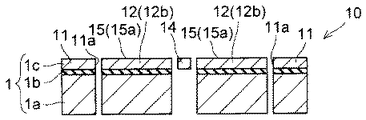
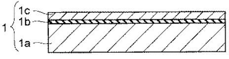
センサ素子10は、図5および図6に示すように、支持基板1a上に絶縁層1bおよびシリコン層1cが順次積層されたSOI(Silicon On Insulator)基板1を、半導体プロセス技術を応用した微細加工技術(MEMS(Micro Electro Mechanical Systems)技術)を用いて加工することにより形成されている。なお、支持基板1aは、たとえば、シリコン基板から構成されており、絶縁層1bは、たとえば、酸化シリコン(SiO2)から構成されている。
As shown in FIGS. 5 and 6, the
また、センサ素子10は、3軸方向の加速度を検出可能なピエゾ抵抗型の加速度センサ素子に構成されている。具体的には、センサ素子10は、図4〜図6に示すように、枠体部11と、枠体部11の内側に配置される重り部12と、重り部12の四方から所定の方向に延びるとともに、重り部12を枠体部11に揺動自在に支持する4つの撓み部13とを備えている。なお、枠体部11は、本発明の「支持枠」の一例であり、重り部12は、本発明の「構造体」の一例である。また、撓み部13は、本発明の「支持部」の一例である。
The
センサ素子10の枠体部11は、図4に示すように、平面的に見て、略矩形枠状に形成されており、中央部に略四角形状の開口部11aを有している。なお、枠体部11は、図5に示すように、支持基板1a、絶縁層1bおよびシリコン層1cから構成されている。
As shown in FIG. 4, the
また、センサ素子10の重り部12は、図4に示すように、枠体部11の内側の開口部11aに配置されている。この重り部12は、図4〜図6に示すように、4つの撓み部13を介して枠体部11に支持された直方体状のコア部12a(図6参照)と、平面的に見て、コア部12aの四隅の各々に一体的に連結された直方体状の4つの付随部12b(図4および図5参照)とを含んでいる。また、付随部12bの各々と枠体部11および撓み部13との間には、隙間が設けられている。この隙間は、加速度を受けて重り部12が揺動した際に、付随部12bが枠体部11や撓み部13と接触しない程度の大きさに構成されている。なお、コア部12aは、本発明の「第1構造体」の一例であり、付随部12bは、本発明の「第2構造体」の一例である。また、重り部12は、枠体部11と同様、支持基板1a、絶縁層1bおよびシリコン層1cから構成されている。
Moreover, the
また、4つの撓み部13の各々は、SOI基板1のシリコン層1cから構成されており、短冊状に形成されている。このため、図6に示すように、撓み部13は、枠体部11よりも厚みが小さくなっており、変形し易くなっている。また、撓み部13の各々は、図4に示すように、一方端部が枠体部11の内側面に一体的に連結されており、他方端部が重り部12(コア部12a)の内側面に一体的に連結されている。なお、4つの撓み部13は、図4に示すように、X軸方向に延びるとともにコア部12aを挟む2つ1組の撓み部13と、Y軸方向に延びるとともにコア部12aを挟む2つ1組の撓み部13とに分けられる。
Each of the four
また、4つの撓み部13の各々の表面には、複数のピエゾ抵抗素子14が形成されている。このピエゾ抵抗素子14は、外力(応力)が加わると抵抗値が変化する素子であり、加速度を受けて重り部12が揺動した際の撓み部13の変位を抵抗値の変化として検出する。すなわち、ピエゾ抵抗型の加速度センサ素子であるセンサ素子10では、加速度が加わるとその加速度によって重り部12が揺動し、重り部12を支持している撓み部13が変形する。そして、撓み部13が変形することによって、撓み部13に形成されているピエゾ抵抗素子14に応力が加わり、ピエゾ抵抗素子14の抵抗値が変化する。この抵抗値の変化を電気信号として検出することにより、半導体装置50に加わった加速度が検出される。
A plurality of
なお、上記した枠体部11、重り部12および撓み部13は、SOI基板1を加工することによって一体的に形成されている。
Note that the
ここで、第1実施形態では、重り部12の上面領域1dおよび枠体部11の上面領域1eに、集積回路15が形成されている。すなわち、コア部12aのシリコン層1cおよび4つの付随部12bの各々のシリコン層1cに集積回路15(15a)が作り込まれているとともに、枠体部11のシリコン層1cの所定領域にも集積回路15(15b)が作り込まれている。この集積回路15は、トランジスタなどの複数の回路素子から構成されている。なお、集積回路15は、本発明の「集積回路部」の一例である。
Here, in the first embodiment, the
また、第1実施形態では、集積回路15は、センサ素子10と電気的に接続されている。具体的には、集積回路15は、ホイートストン・ブリッジ回路に構成されたピエゾ抵抗素子14と図示しない配線層を介して電気的に接続されている。なお、ホイートストン・ブリッジ回路は、複数のピエゾ抵抗素子14を、図示しない配線層を介して電気的に接続することにより構成することができる。また、集積回路15は、センサ素子10によって検出された電気信号を増幅・補正するとともに、加速度に比例した電圧として電気信号を外部に出力する機能を有するように構成されている。
In the first embodiment, the
また、第1実施形態では、枠体部11上の所定領域に複数のパッド電極16が形成されており、図示しない配線層を介して、集積回路15と電気的に接続されている。このパッド電極16は、集積回路15によって増幅・補正された電機信号を外部に出力するための電極端子としての機能を有している。なお、上記した配線層(図示せず)は、所定の配線パターンを有しており、撓み部13のシリコン層1cおよび枠体部11のシリコン層1cなどに設けられている。なお、パッド電極16は、本発明の「電極端子部」の一例である。
In the first embodiment, a plurality of
また、センサ素子10を収納するパッケージ20は、図2および図3に示すように、下部容器21と上部蓋22とから構成されている。下部容器21は、たとえば、積層構造を有するセラミックス製の容器から構成されており、センサ素子10を収納するためのキャビティ(空間部)21aを有している。また、下部容器21の側壁のキャビティ21a側には、下部容器21の上面(上部蓋22が接着される面)よりも低い段差面23が形成されている。この段差面23には、後述するボンディングワイヤ30(図1および図2参照)を介して、センサ素子10のパッド電極16と電気的に接続されるパッド電極24が形成されている。
The
一方、下部容器21の下面には、図2に示すように、図示しない実装基板などにおける配線層と電気的に接続される電極端子25が形成されている。なお、電極端子25と上記したパッド電極24とは、下部容器21内部に形成された配線部26を介して、互いに電気的に接続されている。
On the other hand, as shown in FIG. 2,
また、センサ素子10は、下部容器21のキャビティ21aの底面27における中央部の領域に接着層28を介して固着されている。また、下部容器21のキャビティ21aの底面27とセンサ素子10との間には、接着層28によって、約50μm〜約100μmの高さを有する隙間部29が形成されている。この隙間部29は、センサ素子10の重り部12の動き代を確保するために設けられている。また、下部容器21のキャビティ21a内に収納されたセンサ素子10におけるパッド電極16(図1参照)は、ボンディングワイヤ30を介して、下部容器21のパッド電極24と電気的に接続されている。なお、ボンディングワイヤ30は、たとえば、Au(金)やAl(アルミニウム)などの金属細線から構成されている。
In addition, the
また、下部容器21のキャビティ21aは、上部蓋22によって封止されている。この上部蓋22は、エポキシ樹脂などの熱硬化性樹脂からなる接着層31によって、下部容器21のキャビティ21aを密閉するように下部容器21の上面に固着されている。なお、上部蓋22は、たとえば、42アロイ合金やステンレスなどから構成されている。また、密閉されたパッケージ20の内部は、たとえば窒素ガスやドライエアでパージされている。
Further, the
第1実施形態では、上記のように、重り部12の上面領域1d(シリコン層1c)に、それぞれ、センサ素子10と電気的に接続される集積回路15(15a)を形成することによって、この集積回路15でセンサ素子10からの電気信号を処理して外部に出力することができる。すなわち、上記のように構成することによって、センサ素子10からの電気信号を処理するICチップなどをパッケージ20内に設けることなく、センサ素子10からの電気信号を処理して外部に出力することができる。これにより、ICチップなどをパッケージ20内に設けない構成にすることによって、ICチップなどの収納スペースをパッケージ20内に確保する必要がなくなるので、その分、半導体装置50の小型化を図ることができる。
In the first embodiment, as described above, the integrated circuit 15 (15a) that is electrically connected to the
また、第1実施形態では、上記のように、センサ素子10の枠体部11の内側に配置される重り部12の上面領域1d(シリコン層1c)に集積回路15(15a)を形成することによって、センサ素子10に集積回路15(15a)を形成したとしても、センサ素子10の平面積が大きくなるのを抑制することができる。このため、センサ素子10の平面積が大きくなることに起因して、半導体装置50の平面積が大きくなるという不都合が生じるのを抑制することができるので、半導体装置50の実装面積が大きくなるのを抑制することができるとともに、これによっても、半導体装置50の小型化を図ることができる。
Further, in the first embodiment, as described above, the integrated circuit 15 (15a) is formed in the
また、第1実施形態では、上記のように、重り部12の上面領域1dに加えて、枠体部11の上面領域1eにも集積回路15(15b)を形成することによって、集積回路15の形成領域をより容易に確保することができるので、センサ素子10からの電気的な検出信号を増幅および補正して、加速度に比例した電圧として出力する機能を有する集積回路15をより容易に形成することができる。なお、集積回路15bによっても、集積回路15aと同様、センサ素子10からの電気信号を処理して外部に出力することができる。
In the first embodiment, as described above, the integrated circuit 15 (15b) is formed not only in the
図7〜図10は、本発明の第1実施形態による半導体装置のセンサ素子の製造方法を説明するための図である。なお、図9および図10は、図8の80−80線に沿った断面に対応する断面を示している。次に、図1、図5および図7〜図10を参照して、第1実施形態による半導体装置50のセンサ素子10の製造方法について説明する。
7 to 10 are views for explaining a method of manufacturing the sensor element of the semiconductor device according to the first embodiment of the present invention. 9 and 10 show a cross section corresponding to the cross section taken along the line 80-80 in FIG. A method for manufacturing the
まず、図7に示すように、シリコン基板からなる支持基板1aの上面上に、SiO2からなる絶縁層1bおよびシリコン層1cを順次積層することによって、SOI基板1を形成する。
First, as shown in FIG. 7, an
次に、図8に示すように、SOI基板1の上面(シリコン層1c)に、集積回路15、ピエゾ抵抗素子14、パッド電極16および配線層(図示せず)をそれぞれ形成する。具体的には、シリコン層1cに、フォトリソグラフィ技術、エッチング技術および不純物拡散技術などを用いてトランジスタなどの複数の回路素子を作り込むことにより、重り部12(図1参照)に対応する領域および枠体部11(図1参照)に対応する所定領域に集積回路15を形成する。また、フォトリソグラフィ技術および不純物拡散技術などを用いて、撓み部13に対応する所定領域にピエゾ抵抗素子14を形成するとともに、ホイートストン・ブリッジ回路を構成するための配線層(図示せず)を形成する。また、蒸着法などを用いて、枠体部11に対応する所定領域にパッド電極16を形成する。さらに、不純物拡散技術などを用いて、集積回路15とピエゾ抵抗素子14とを電気的に接続する配線層(図示せず)および集積回路15とパッド電極16とを電気的に接続する配線層(図示せず)などを形成する。
Next, as shown in FIG. 8, an
次に、集積回路15、ピエゾ抵抗素子14および配線層(図示せず)などを保護した後、図9に示すように、SOI基板1の上面側から絶縁層1bに達する深さまで、絶縁層1bをエッチングストップ層としてエッチングすることにより、シリコン層1cの所定領域を除去する。これにより、SOI基板1におけるシリコン層1cがパターニングされて、枠体部11(図5参照)に対応する部位、撓み部13(図5参照)に対応する部位および重り部12(図5参照)に対応する部位が残る。なお、上記したパターニングは、たとえば、誘導結合プラズマ(ICP)型のドライエッチング装置を用いたドライエッチングにより行うことができる。その際、エッチング条件としては、絶縁層1bがエッチングストップ層として機能するような条件に設定する。
Next, after protecting the
続いて、図10に示すように、SOI基板1の下面側から絶縁層1bに達する深さまで、絶縁層1bをエッチングストップ層としてエッチングすることにより、シリコン層1cの所定領域を除去する。これにより、SOI基板1における支持基板1aがパターニングされて、枠体部11(図5参照)に対応する部位および重り部12(図5参照)に対応する部位が残る。なお、上記したパターニングは、たとえば、誘導結合プラズマ(ICP)型のドライエッチング装置を用いたドライエッチングにより行うことができる。その際、エッチング条件としては、絶縁層1bがエッチングストップ層として機能するような条件に設定する。
Subsequently, as shown in FIG. 10, a predetermined region of the
最後に、SOI基板1の絶縁層1bを、枠体部11および重り部12に対応する領域以外の領域をエッチングにより除去することにより、図5に示した形状を得る。このようにして、図1に示した本発明の第1実施形態による半導体装置50のセンサ素子10が形成される。
Finally, the insulating
(第2実施形態)
図11は、本発明の第2実施形態による半導体装置の平面図である。図12は、本発明の第2実施形態による半導体装置のセンサ素子の全体斜視図である。図13は、本発明の第2実施形態による半導体装置のセンサ素子の平面図である。次に、図11〜図13を参照して、本発明の第2実施形態による半導体装置100の構造について説明する。
(Second Embodiment)
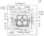
FIG. 11 is a plan view of a semiconductor device according to a second embodiment of the present invention. FIG. 12 is an overall perspective view of the sensor element of the semiconductor device according to the second embodiment of the present invention. FIG. 13 is a plan view of a sensor element of the semiconductor device according to the second embodiment of the present invention. Next, the structure of the
この第2実施形態による半導体装置100では、図11〜図13に示すように、センサ素子110の重り部12(付随部12b)の一部が連結部111を介して、センサ素子110の枠体部11と連結されている。具体的には、4つの付随部12bのうちの1つの付随部12bの角部が、連結部111によって、枠体部11の内側面と一体的に連結されている。この連結部111は、シリコン層1cを含むように構成されている。
In the
また、連結部111は、集積回路15とパッド電極16とを電気的に接続するための接続経路として機能するように構成されている。具体的には、重り部12の上面領域1dには集積回路15(15a)が形成されているとともに、枠体部11の所定領域および連結部111の所定領域には、所定の配線パターンを有する配線層112が形成されている。そして、この配線層112によって、集積回路15とパッド電極16とが電気的に接続されている。
In addition, the connecting
また、上記した連結部111は、上記第1実施形態によるセンサ素子110の製造方法において、SOI基板1のパターニングを変更することによって形成することができる。
In addition, the connecting
なお、上記した第2実施形態の構成では、センサ素子110に連結部111を設けることによって重り部12の所定方向への揺動動作が制限されるので、センサ素子110を、3軸方向以外の2軸方向または1軸方向の加速度を検出する加速度センサ素子として用いてもよい。この場合、パッド電極16および24の数を少なくすることができる。また、所定方向への揺動動作の制限された分だけ、集積回路15によって補正することにより、3軸方向の加速度を検出する加速度センサ素子として用いることもできる。
In the configuration of the second embodiment described above, the connecting
第2実施形態による半導体装置100のその他の構成は、上記第1実施形態と同様である。
Other configurations of the
第2実施形態では、上記のように、4つの付随部12bのうちの1つの付随部12bの角部を、連結部111により連結することによって、連結部111を、集積回路15と枠体部11のパッド電極16とを電気的に接続するための接続経路として機能させることができる。このため、連結部111を介して、配線層112により、集積回路15と枠体部11のパッド電極16とを容易に電気的に接続することができるので、集積回路15によって処理されたセンサ素子110からの電気信号をパッド電極16を介して容易に外部に出力することができる。これにより、容易に、ICチップなどをパッケージ内に設けない構成にすることができるので、容易に、半導体装置100を小型化することができる。
In the second embodiment, as described above, the connecting
第2実施形態による半導体装置100のその他の効果は、上記第1実施形態と同様である。
Other effects of the
なお、今回開示された実施形態は、すべての点で例示であって制限的なものではないと考えられるべきである。本発明の範囲は、上記した実施形態の説明ではなく特許請求の範囲によって示され、さらに特許請求の範囲と均等の意味および範囲内でのすべての変更が含まれる。 The embodiment disclosed this time should be considered as illustrative in all points and not restrictive. The scope of the present invention is shown not by the above description of the embodiments but by the scope of claims for patent, and further includes all modifications within the meaning and scope equivalent to the scope of claims for patent.
たとえば、上記第1および第2実施形態では、ピエゾ抵抗型の加速度センサ素子を備えた半導体装置に本発明を適用した例を示したが、本発明はこれに限らず、ピエゾ抵抗型以外の加速度センサ素子を備えた半導体装置に本発明を適用してもよい。 For example, in the first and second embodiments, an example in which the present invention is applied to a semiconductor device including a piezoresistive acceleration sensor element has been described. However, the present invention is not limited to this, and accelerations other than the piezoresistive type are shown. The present invention may be applied to a semiconductor device provided with a sensor element.
また、上記第1および第2実施形態では、重り部の上面領域のほぼ全面(コア部の上面領域および複数の付随部の上面領域の各々)に、集積回路を形成した例を示したが、本発明はこれに限らず、重り部の上面領域の一部に集積回路を形成するようにしてもよい。 In the first and second embodiments, the example in which the integrated circuit is formed on almost the entire upper surface region of the weight portion (each of the upper surface region of the core portion and the upper surface region of the plurality of associated portions) is shown. The present invention is not limited to this, and an integrated circuit may be formed in a part of the upper surface region of the weight portion.
また、上記第1および第2実施形態では、集積回路を、センサ素子によって検出された電気信号を増幅・補正するとともに、加速度に比例した電圧として電気信号を外部に出力する機能を有するように構成した例を示したが、本発明はこれに限らず、集積回路を、上記した機能とは異なる機能を有するように構成してもよい。また、集積回路を、上記した機能に加えて、他の機能を有するように構成してもよい。 In the first and second embodiments, the integrated circuit has a function of amplifying and correcting the electric signal detected by the sensor element and outputting the electric signal to the outside as a voltage proportional to the acceleration. However, the present invention is not limited to this, and the integrated circuit may be configured to have a function different from the above function. Further, the integrated circuit may be configured to have other functions in addition to the functions described above.
また、上記第1実施形態では、集積回路を、重り部の上面領域に加えて、枠体部の上面領域にも形成した例を示したが、本発明はこれに限らず、枠体部の上面領域に集積回路を形成しない構成にしてもよい。 In the first embodiment, the example in which the integrated circuit is formed not only in the upper surface area of the weight part but also in the upper surface area of the frame body part is shown. An integrated circuit may not be formed in the upper surface region.
また、上記第1実施形態では、3軸方向の加速度を検出可能なセンサ素子を用いることによって、半導体装置を3軸加速度センサに構成した例を示したが、本発明はこれに限らず、3軸型方向以外の2軸方向または1軸方向の加速度を検出可能なセンサ素子を用いることによって、半導体装置を2軸加速度センサまたは1軸加速度センサに構成してもよい。 In the first embodiment, the example in which the semiconductor device is configured as a three-axis acceleration sensor by using a sensor element capable of detecting acceleration in the three-axis direction has been described. The semiconductor device may be configured as a two-axis acceleration sensor or a one-axis acceleration sensor by using a sensor element that can detect acceleration in two-axis directions or one-axis direction other than the axial direction.
また、上記第2実施形態では、1つの付随部の一部が連結部によって枠体部と連結されたセンサ素子の構成について示したが、本発明はこれに限らず、センサ素子の重り部が揺動可能であれば、センサ素子の構成は、上記した構成以外の構成であってもよい。すなわち、たとえば、複数の付随部が連結部によって枠体部と連結された構成であってもよい。 Further, in the second embodiment, the configuration of the sensor element in which a part of one associated part is connected to the frame body part by the connecting part is shown, but the present invention is not limited to this, and the weight part of the sensor element is The configuration of the sensor element may be other than the configuration described above as long as it can swing. That is, for example, a configuration in which a plurality of accompanying parts are connected to the frame part by a connecting part may be used.
1 SOI基板
1a 支持基板
1b 絶縁層
1c シリコン層
1d、1e 上面領域
10、110 センサ素子
11 枠体部(支持枠)
12 重り部(構造体)
12a コア部(第1構造体)
12b 付随部(第2構造体)
13 撓み部(梁部)
14 ピエゾ抵抗素子
15、15a、15b 集積回路(集積回路部)
16 パッド電極(電極端子部)
20 パッケージ
21 下部容器
21a キャビティ
22 上部蓋
30 ボンディングワイヤ
50、100 半導体装置
111 連結部
112 配線層
DESCRIPTION OF
12 Weight part (structure)
12a Core part (first structure)
12b Accompanying part (second structure)
13 Deflection part (beam part)
14
16 Pad electrode (electrode terminal part)
20
Claims (33)
前記センサ素子を収納するパッケージとを備え、
前記センサ素子は、支持枠と、前記支持枠の内側に配置される構造体と、前記構造体を前記支持枠に揺動可能に支持する梁部とを含み、
少なくとも前記構造体の上面領域の一部には、前記センサ素子と電気的に接続される集積回路部が形成されており、
前記構造体は、前記梁部を介して前記支持枠に支持される直方体状の第1構造体と、前記第1構造体に一体的に連結される直方体状の複数の第2構造体とを含み、
前記集積回路部は、前記複数の第2構造体の少なくとも1つの上面領域に形成されており、
前記支持枠の上面領域には、電極端子部が設けられているとともに、前記複数の第2構造体の一部と前記支持枠とは、連結部によって連結されており、
前記連結部は、前記支持枠の前記電極端子部と前記集積回路部とを電気的に接続するための接続経路として機能するように構成されており、
前記第2構造体のうちの1つの前記第2構造体の角部が、前記連結部によって支持枠の内側面と一体的に連結されており、
前記支持枠の所定領域および前記連結部の所定領域には、所定の配線パターンを有する配線層が形成されており、この配線層によって、前記集積回路部と前記電極端子部とが電気的に接続されていることを特徴とする、半導体装置。 A sensor element made of silicon formed using semiconductor process technology;
A package for housing the sensor element;
The sensor element includes a support frame, a structure disposed inside the support frame, and a beam portion that swingably supports the structure on the support frame,
An integrated circuit portion that is electrically connected to the sensor element is formed at least in a part of the upper surface region of the structure ,
The structure includes a rectangular parallelepiped first structure supported by the support frame via the beam portion, and a plurality of rectangular parallelepiped second structures integrally connected to the first structure. Including
The integrated circuit portion is formed in at least one upper surface region of the plurality of second structures,
An electrode terminal portion is provided in the upper surface region of the support frame, and a part of the plurality of second structures and the support frame are connected by a connecting portion,
The connecting portion is configured to function as a connection path for electrically connecting the electrode terminal portion of the support frame and the integrated circuit portion,
A corner portion of one of the second structures is integrally connected to an inner surface of a support frame by the connecting portion,
A wiring layer having a predetermined wiring pattern is formed in a predetermined region of the support frame and a predetermined region of the connecting portion, and the integrated circuit portion and the electrode terminal portion are electrically connected by the wiring layer. A semiconductor device, wherein
Priority Applications (2)
| Application Number | Priority Date | Filing Date | Title |
|---|---|---|---|
| JP2007235269A JP5118923B2 (en) | 2007-09-11 | 2007-09-11 | Semiconductor device |
| PCT/JP2008/065652 WO2009034863A1 (en) | 2007-09-11 | 2008-09-01 | Semiconductor device |
Applications Claiming Priority (1)
| Application Number | Priority Date | Filing Date | Title |
|---|---|---|---|
| JP2007235269A JP5118923B2 (en) | 2007-09-11 | 2007-09-11 | Semiconductor device |
Publications (3)
| Publication Number | Publication Date |
|---|---|
| JP2009068893A JP2009068893A (en) | 2009-04-02 |
| JP2009068893A5 JP2009068893A5 (en) | 2010-10-14 |
| JP5118923B2 true JP5118923B2 (en) | 2013-01-16 |
Family
ID=40451872
Family Applications (1)
| Application Number | Title | Priority Date | Filing Date |
|---|---|---|---|
| JP2007235269A Expired - Fee Related JP5118923B2 (en) | 2007-09-11 | 2007-09-11 | Semiconductor device |
Country Status (2)
| Country | Link |
|---|---|
| JP (1) | JP5118923B2 (en) |
| WO (1) | WO2009034863A1 (en) |
Families Citing this family (2)
| Publication number | Priority date | Publication date | Assignee | Title |
|---|---|---|---|---|
| KR101071915B1 (en) | 2009-07-06 | 2011-10-11 | 주식회사 이노칩테크놀로지 | Acceleration sensor and method for manufacturing the same |
| KR101132263B1 (en) | 2010-01-08 | 2012-04-02 | 주식회사 이노칩테크놀로지 | Assembly for acceleration sensing and method for manufacturing the same |
Family Cites Families (5)
| Publication number | Priority date | Publication date | Assignee | Title |
|---|---|---|---|---|
| JP2505987Y2 (en) * | 1989-12-28 | 1996-08-07 | 株式会社ワコー | Acceleration sensor |
| JP3478894B2 (en) * | 1995-02-20 | 2003-12-15 | 株式会社東海理化電機製作所 | Surface type acceleration sensor |
| JPH08327657A (en) * | 1995-06-01 | 1996-12-13 | Nikon Corp | Mechanical quantity sensor |
| JP2007035965A (en) * | 2005-07-27 | 2007-02-08 | Oki Electric Ind Co Ltd | Semiconductor device, adhesive material and their manufacturing methods |
| JP3938202B1 (en) * | 2006-03-28 | 2007-06-27 | 松下電工株式会社 | Manufacturing method of sensor package |
-
2007
- 2007-09-11 JP JP2007235269A patent/JP5118923B2/en not_active Expired - Fee Related
-
2008
- 2008-09-01 WO PCT/JP2008/065652 patent/WO2009034863A1/en active Application Filing
Also Published As
| Publication number | Publication date |
|---|---|
| JP2009068893A (en) | 2009-04-02 |
| WO2009034863A1 (en) | 2009-03-19 |
Similar Documents
| Publication | Publication Date | Title |
|---|---|---|
| JP4670427B2 (en) | Semiconductor sensor and manufacturing method thereof | |
| JP5486271B2 (en) | Acceleration sensor and method of manufacturing acceleration sensor | |
| KR100985453B1 (en) | Sensor device and production method therefor | |
| JP4754817B2 (en) | Semiconductor acceleration sensor | |
| JP6468167B2 (en) | Mechanical quantity sensor | |
| JP2006170856A (en) | Acceleration sensor | |
| JP6209270B2 (en) | Acceleration sensor | |
| JP5118923B2 (en) | Semiconductor device | |
| JP2005127750A (en) | Semiconductor sensor and its manufacturing method | |
| JP3938199B1 (en) | Wafer level package structure and sensor device | |
| JP4428210B2 (en) | Mounting structure of physical quantity sensor | |
| JP3938205B1 (en) | Sensor element | |
| JP2008122304A (en) | Electrostatic capacitance type acceleration sensor | |
| JP6464770B2 (en) | Physical quantity sensor and manufacturing method thereof | |
| JP5843302B1 (en) | Manufacturing method of composite sensor device | |
| JP4706634B2 (en) | Semiconductor sensor and manufacturing method thereof | |
| JP4665733B2 (en) | Sensor element | |
| JP4466344B2 (en) | Acceleration sensor | |
| JP2007263767A (en) | Sensor device | |
| JP5678535B2 (en) | Mechanical quantity sensor and method of manufacturing mechanical quantity sensor | |
| JP5069410B2 (en) | Sensor element | |
| JP5167848B2 (en) | Support substrate and method of manufacturing capacitive mechanical quantity detection sensor using the same | |
| JP2016170100A (en) | Glass substrate with embedded silicon wiring and sensor using the same | |
| JP4000170B2 (en) | Chip size package | |
| JP3938200B1 (en) | Sensor device and manufacturing method thereof |
Legal Events
| Date | Code | Title | Description |
|---|---|---|---|
| A521 | Written amendment |
Free format text: JAPANESE INTERMEDIATE CODE: A523 Effective date: 20100830 |
|
| A621 | Written request for application examination |
Free format text: JAPANESE INTERMEDIATE CODE: A621 Effective date: 20100831 |
|
| A131 | Notification of reasons for refusal |
Free format text: JAPANESE INTERMEDIATE CODE: A131 Effective date: 20120703 |
|
| A521 | Written amendment |
Free format text: JAPANESE INTERMEDIATE CODE: A523 Effective date: 20120829 |
|
| TRDD | Decision of grant or rejection written | ||
| A01 | Written decision to grant a patent or to grant a registration (utility model) |
Free format text: JAPANESE INTERMEDIATE CODE: A01 Effective date: 20120925 |
|
| A01 | Written decision to grant a patent or to grant a registration (utility model) |
Free format text: JAPANESE INTERMEDIATE CODE: A01 |
|
| A61 | First payment of annual fees (during grant procedure) |
Free format text: JAPANESE INTERMEDIATE CODE: A61 Effective date: 20121022 |
|
| R150 | Certificate of patent or registration of utility model |
Ref document number: 5118923 Country of ref document: JP Free format text: JAPANESE INTERMEDIATE CODE: R150 Free format text: JAPANESE INTERMEDIATE CODE: R150 |
|
| FPAY | Renewal fee payment (event date is renewal date of database) |
Free format text: PAYMENT UNTIL: 20151026 Year of fee payment: 3 |
|
| R250 | Receipt of annual fees |
Free format text: JAPANESE INTERMEDIATE CODE: R250 |
|
| RD03 | Notification of appointment of power of attorney |
Free format text: JAPANESE INTERMEDIATE CODE: R3D03 |
|
| LAPS | Cancellation because of no payment of annual fees |