JP5118407B2 - Optical system, exposure apparatus, and device manufacturing method - Google Patents
Optical system, exposure apparatus, and device manufacturing method Download PDFInfo
- Publication number
- JP5118407B2 JP5118407B2 JP2007199894A JP2007199894A JP5118407B2 JP 5118407 B2 JP5118407 B2 JP 5118407B2 JP 2007199894 A JP2007199894 A JP 2007199894A JP 2007199894 A JP2007199894 A JP 2007199894A JP 5118407 B2 JP5118407 B2 JP 5118407B2
- Authority
- JP
- Japan
- Prior art keywords
- refractive optical
- optical system
- refractive
- optical
- optical member
- Prior art date
- Legal status (The legal status is an assumption and is not a legal conclusion. Google has not performed a legal analysis and makes no representation as to the accuracy of the status listed.)
- Expired - Fee Related
Links
Images


Classifications
-
- G—PHYSICS
- G03—PHOTOGRAPHY; CINEMATOGRAPHY; ANALOGOUS TECHNIQUES USING WAVES OTHER THAN OPTICAL WAVES; ELECTROGRAPHY; HOLOGRAPHY
- G03F—PHOTOMECHANICAL PRODUCTION OF TEXTURED OR PATTERNED SURFACES, e.g. FOR PRINTING, FOR PROCESSING OF SEMICONDUCTOR DEVICES; MATERIALS THEREFOR; ORIGINALS THEREFOR; APPARATUS SPECIALLY ADAPTED THEREFOR
- G03F7/00—Photomechanical, e.g. photolithographic, production of textured or patterned surfaces, e.g. printing surfaces; Materials therefor, e.g. comprising photoresists; Apparatus specially adapted therefor
- G03F7/70—Microphotolithographic exposure; Apparatus therefor
- G03F7/70216—Mask projection systems
- G03F7/70241—Optical aspects of refractive lens systems, i.e. comprising only refractive elements
-
- G—PHYSICS
- G03—PHOTOGRAPHY; CINEMATOGRAPHY; ANALOGOUS TECHNIQUES USING WAVES OTHER THAN OPTICAL WAVES; ELECTROGRAPHY; HOLOGRAPHY
- G03F—PHOTOMECHANICAL PRODUCTION OF TEXTURED OR PATTERNED SURFACES, e.g. FOR PRINTING, FOR PROCESSING OF SEMICONDUCTOR DEVICES; MATERIALS THEREFOR; ORIGINALS THEREFOR; APPARATUS SPECIALLY ADAPTED THEREFOR
- G03F7/00—Photomechanical, e.g. photolithographic, production of textured or patterned surfaces, e.g. printing surfaces; Materials therefor, e.g. comprising photoresists; Apparatus specially adapted therefor
- G03F7/70—Microphotolithographic exposure; Apparatus therefor
- G03F7/70216—Mask projection systems
- G03F7/70233—Optical aspects of catoptric systems, i.e. comprising only reflective elements, e.g. extreme ultraviolet [EUV] projection systems
Description
本発明は、原版のパターンを光学系を介して基板に露光する露光装置やデバイス製造方法に関する。 The present invention relates to an exposure apparatus and a device manufacturing method for exposing an original pattern to a substrate via an optical system.
露光装置は、ICやLSI等の半導体チップ、液晶パネル等の表示素子、磁気ヘッド等の検出素子、CCD等の撮像素子といった各種デバイス、マイクロメカニクスで用いる微細パターンの製造に用いられる。これら素子は、レチクルのパターンを投影光学系を介してフォトレジストが塗布された基板上に投影することにより製造される。 The exposure apparatus is used to manufacture various devices such as semiconductor chips such as IC and LSI, display elements such as liquid crystal panels, detection elements such as magnetic heads, imaging elements such as CCDs, and fine patterns used in micromechanics. These elements are manufactured by projecting a reticle pattern onto a substrate coated with a photoresist via a projection optical system.
従来の投影光学系として、例えば同心又は非同心の凹面鏡や凸面鏡を使用した反射光学系や、凹面鏡や凸面鏡の他に負のメニスカスレンズ及び色収差補正機構を加えた略同心の反射光学系等が知られている。 Known conventional projection optical systems include, for example, a reflective optical system using concentric or non-concentric concave mirrors and convex mirrors, and a substantially concentric reflective optical system including a negative meniscus lens and a chromatic aberration correction mechanism in addition to concave and convex mirrors. It has been.
これらの反射光学系は軸外の半弧状態領域に良像域が形成されている。そして、この良像域に対応するレチクルのパターン像を基板上に形成するし、レチクル及び基板を一体として反射光学系に対して相対的に走査することによりレチクルのパターン像全体を基板上に形成するアライナが知られている。 In these reflection optical systems, a good image area is formed in an off-axis semi-arc state area. Then, a reticle pattern image corresponding to the good image area is formed on the substrate, and the entire reticle pattern image is formed on the substrate by scanning the reticle and the substrate as a whole with respect to the reflection optical system. An aligner to do is known.
しかしながら、従来の反射光学系のいずれも非点隔差及び像面湾曲が大きく、そのために良像域の幅は極めて狭く、アライナに適用した場合に多くの走査時間、即ち露光時間を必要とし、時間当たりの基板焼付け処理量が比較的少ないという難点があった。 However, all of the conventional reflection optical systems have large astigmatism and curvature of field, so that the width of the good image area is extremely narrow, and when applied to an aligner, a lot of scanning time, that is, exposure time is required. There was a problem that the amount of substrate baking processing per hit was relatively small.
従来の投影光学系は、特許文献1,2のように、凸面鏡及びメニスカスレンズを含む凸ユニットと屈折光学部材とで構成されている。特に、特許文献1では、ミラーを球面とし凹面鏡と凸面鏡との間に非球面光学素子を配置することで良像域の拡大を達成している。また、特許文献2では、拡大投影倍率を有する反射屈折光学系において凹面鏡と凸面鏡との間に非球面光学素子を配置することで良像域の拡大と色収差の補正を達成している。
上記従来技術によって、大型基板であっても基板焼付け処理量が低下しない露光装置の設計が可能になる。しかしながら、装置の大型化等に伴い、光学部材の組み付け誤差や製作誤差等が原因で画角に依存する収差、即ち、非点間差(非点収差)及びディストーション(歪曲収差)が発生しやすくなる。 According to the above-described conventional technology, it is possible to design an exposure apparatus that does not reduce the amount of substrate baking processing even for a large substrate. However, as the apparatus becomes larger, aberrations that depend on the angle of view, that is, astigmatism (distortion) and distortion (distortion) are likely to occur due to assembly errors and manufacturing errors of the optical members. Become.
従来は凸面鏡若しくは凸ユニットの位置を調整することにより非点隔差及びディストーションの調整、又は像面や物面近くに配置された平面ガラスを曲げることによってディストーションの調整を行っている。 Conventionally, the astigmatic difference and distortion are adjusted by adjusting the position of the convex mirror or the convex unit, or the distortion is adjusted by bending a flat glass disposed near the image plane or the object plane.
しかしながら、装置の大型化に伴い調整を行う成分以外の他成分の収差が無視できない量発生する等満足できる調整精度を得ることができない場合があった。 However, there have been cases where satisfactory adjustment accuracy cannot be obtained, for example, aberrations of components other than the component to be adjusted are generated in a non-negligible amount as the apparatus becomes larger.
本発明は、上記課題に鑑みてなされ、その目的は、良像域を拡大するために物面と像面の近傍に配置された屈折光学部材を光軸に直交する面内に移動させることにより、ディストーション及び/又は非点隔差を高精度に調整できる技術を実現することである。 The present invention has been made in view of the above problems, and its object is to move a refractive optical member disposed in the vicinity of the object surface and the image plane in a plane perpendicular to the optical axis in order to enlarge the good image area. It is to realize a technique capable of adjusting distortion and / or astigmatism with high accuracy.
上記課題を解決し、目的を達成するために、本発明の光学系は、物体面の像を像面に投影する光学系であって、前記物体面側に配置された少なくとも1つの第1屈折光学部材を含み、かつ、前記像面側に配置された少なくとも1つの第2屈折光学部材を含み、前記第1屈折光学部材及び前記第2屈折光学部材を光軸方向に対して垂直な方向に移動することによって、前記光学系の非点隔差及びディストーションを独立して調整を行う調整手段を有し、前記調整手段は、ある像高において前記第1屈折光学部材の前記光軸方向に対して垂直な方向への移動によるディストーションの発生量と前記第2屈折光学部材の前記光軸方向に対して垂直な方向への移動によるディストーションの発生量とが異符号となり合計のディストーションの発生量が一方の発生量より小さくなるように、前記第1屈折光学部材及び前記第2屈折光学部材を移動して、前記光学系の非点隔差を調整し、または、ある像高において前記第1屈折光学部材の前記光軸方向に対して垂直な方向への移動による非点隔差の発生量と前記第2屈折光学部材の前記光軸方向に対して垂直な方向への移動による非点隔差の発生量とが異符号となり合計の非点隔差の発生量が一方の発生量より小さくなるように、前記第1屈折光学部材及び前記第2屈折光学部材を移動して、前記光学系のディストーションを調整する。 In order to solve the above problems and achieve the object, an optical system of the present invention is an optical system for projecting an image of an object plane onto an image plane, and at least one first refraction disposed on the object plane side. It includes an optical member, and includes at least one second refractive optical member disposed on the image plane side, toward perpendicular to the first refractive optical element and the second refractive optical member with respect to the optical axis By adjusting the astigmatic difference and distortion of the optical system independently by moving in the direction of the optical system, and the adjusting means is arranged in the optical axis direction of the first refractive optical member at a certain image height. The amount of distortion generated due to the movement in the direction perpendicular to the amount of distortion and the amount of distortion generated due to the movement of the second refractive optical member in the direction perpendicular to the optical axis direction have different signs , and the total amount of distortion generated But As square smaller than the amount of generation of the first refractive optical element and by moving the second refractive optical element, and adjust the astigmatism of the optical system, or the first refractive optical in certain image height Generation amount of astigmatism due to movement of the member in a direction perpendicular to the optical axis direction and generation amount of astigmatism due to movement of the second refractive optical member in a direction perpendicular to the optical axis direction And the first refractive optical member and the second refractive optical member are moved to adjust the distortion of the optical system so that the generation of the total astigmatism becomes smaller than one of the generations. .
また、本発明の露光装置は、上記光学系を有し、原版のパターンを前記光学系を介して基板に露光する。 An exposure apparatus of the present invention has the above optical system, and exposes a pattern of an original on a substrate through the optical system.
また、本発明のデバイス製造方法は、上記露光装置を用いて基板を露光するステップと、露光された前記基板を現像するステップと、を有する。 The device manufacturing method of the present invention includes a step of exposing a substrate using the exposure apparatus, and a step of developing the exposed substrate.
本発明によれば、良像域を拡大するために物面と像面の近傍に配置された屈折光学部材を光軸に直交する面内に移動させることにより、ディストーション及び/又は非点隔差を高精度に調整することができる。 According to the present invention, in order to enlarge the good image area, the refracting optical member arranged in the vicinity of the object surface and the image surface is moved in a plane orthogonal to the optical axis, thereby reducing distortion and / or astigmatism. It can be adjusted with high accuracy.
以下に、添付図面を参照して本発明を実施するための最良の形態について詳細に説明する。 The best mode for carrying out the present invention will be described below in detail with reference to the accompanying drawings.
尚、以下に説明する実施の形態は、本発明を実現するための一例であり、本発明が適用される装置の構成や各種条件によって適宜修正又は変更されるべきものであり、本発明は以下の実施の形態に限定されるものではない。 The embodiment described below is an example for realizing the present invention, and should be appropriately modified or changed according to the configuration and various conditions of the apparatus to which the present invention is applied. It is not limited to the embodiment.
[第1の実施形態]
第1の実施形態は屈折光学素子が球面レンズであり、屈折光学素子の光線有効部が光軸を含まない軸外に存在する光学系の構成例である。
[First embodiment]
The first embodiment is a configuration example of an optical system in which the refractive optical element is a spherical lens, and the light ray effective portion of the refractive optical element exists outside the axis not including the optical axis.
図1は第1の実施形態の光学系の構成を示している。 FIG. 1 shows the configuration of the optical system of the first embodiment.
図1において、光学系は、第1屈折光学部材1、第1凹反射面(ミラー)3、凸反射面(ミラー)5、第2屈折光学部材6を介して像を形成する。第1、第2屈折光学部材1,6は光軸方向に直交するY,Z面内で移動可能に保持され、光学系の非点隔差及びディストーションの少なくともいずれかの調整が可能である。
In FIG. 1, the optical system forms an image via a first refractive
尚、図1の光学系においてX軸は紙面内左右方向、Y軸は紙面内上下方向、Z軸は紙面垂直方向とする。 In the optical system of FIG. 1, the X axis is the left-right direction in the drawing, the Y axis is the up-down direction in the drawing, and the Z axis is the direction perpendicular to the drawing.
以下、表1に軸外良像域を使用する反射屈折投影系の光学データを示す。Noは光学面番号を表し、Noに付随しているASPは非球面レンズであることを示す。r欄は各項が面の曲率半径を表し∞は平面を表している。d欄は次の光学面との光軸上の距離を表し、光の進む方向を正とし1回反射するごとに符号が反転する。n欄は次の光学面との間の屈折率を表している。 Table 1 below shows optical data of a catadioptric projection system using an off-axis good image area. No represents an optical surface number, and ASP attached to No represents an aspheric lens. In the r column, each term represents the radius of curvature of the surface, and ∞ represents the plane. d column represents a distance on the optical axis of the next optical surface, sign-is inverted each time reflecting the direction of travel of light is positive once. Column n represents the refractive index between the next optical surface.
使用波長はi線、h線、g線から1つ又は複数選択又は選択せず全て使用可能であり、それその波長に対する石英の屈折率を1.4745、1.4696、1.4668とする。本実施形態では良像域の光軸からの高さを240mmとする。 The wavelength used can be selected from i-line, h-line, or g-line without selecting or selecting one, and the refractive index of quartz for the wavelength is 1.4745, 1.4696, 1.4668. In this embodiment, the height of the good image area from the optical axis is 240 mm.

また、ASPの非球面形状は式1により表現でき、それぞれの非球面係数は表2のようになる。
The ASP aspherical shape can be expressed by
X:接平面から非球面までの光軸方向距離
k:円錐係数
h:光軸からの高さ
r:曲率半径
A,B,C,D,E,F,G:非球面係数
X: optical axis direction distance from tangential plane to aspherical surface k: conical coefficient h: height from optical axis r: radius of curvature A, B, C, D, E, F, G: aspherical coefficient
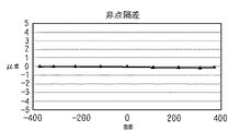
図1の構成において、例えば第1屈折光学部材1がZプラス方向に300μm移動した場合、ディストーションは図2のように変化し、非点隔差は図3のように変化する。同様に、第2屈折光学部材6がZプラス方向に300μm移動した場合、ディストーションは図4のように変化し、非点隔差は図5のように変化する。
In the configuration of FIG. 1, for example, when the first refractive
ディストーションとは理想結像点からのY,Z面内へのズレ量であり、非点隔差とは縦方向(Y方向)パターンと横方向(Z方向)パターンの結像点の光方向のズレと定義する。 Distortion is the amount of deviation from the ideal imaging point into the Y and Z planes, and astigmatic difference is the deviation in the light direction between the imaging points of the vertical (Y direction) pattern and the horizontal (Z direction) pattern. It is defined as
グラフ横軸座標は露光領域のZ軸座標を示しており、グラフ縦軸は非点隔差又はディストーションの発生量を示す。以下のグラフについても同様である。 The horizontal axis of the graph indicates the Z-axis coordinate of the exposure area, and the vertical axis of the graph indicates the amount of astigmatic difference or distortion. The same applies to the following graphs.
図6及び図7に示すように、上記第1屈折光学部材1の移動と第2屈折光学部材6の移動を同時にZプラス方向に300μm行うと非点隔差は図7のように実質的に変化せず、主としてディストーションが図2と図4の加算分だけ図6のように変化する。
As shown in FIGS. 6 and 7, when the movement of the first refractive
図8及び図9に示すように、例えば、第1屈折光学部材1がZプラス方向に300μm移動し、第2屈折光学部材6がZマイナス方向に300μm移動した場合にディストーションは図8のように実質的に変化せず、主として非点隔差が図9のように変化する。
As shown in FIGS. 8 and 9, for example, when the first refractive
即ち、上記第1及び第2屈折光学部材1,6を、ディストーション又は非点隔差の変化が異符号となる方向に同時に移動させ、かつ、ディストーション又は非点隔差の量の絶対値が略同じになるように移動させる。これにより、ディストーション非点隔差を変化させることなく非点隔差又はディストーションを調整することができる。
That is, the first and second refractive
ここで、上記第1及び第2屈折光学部材1,6を同時に移動させたときのディストーション又は非点隔差は、当該第1及び第2屈折光学部材1,6のいずれかを移動させたときに発生するディストーション又は非点隔差の1/2以下となる。
Here, the distortion or astigmatic difference when the first and second refractive
以上はZ方向について述べたがX方向、Y方向についても、第1、第2屈折光学部材1,6を移動することで非点隔差及び/又はディストーションを変化させることができる。
Although the Z direction has been described above, astigmatism and / or distortion can be changed by moving the first and second refractive
[第2の実施形態]
第2の実施形態は屈折光学素子がパワーを持たない非球面レンズであり、屈折光学素子の光線有効部が光軸を含まない軸外に存在する光学系の構成例である。
[Second Embodiment]
The second embodiment is an example of the configuration of an optical system in which the refractive optical element is an aspherical lens having no power, and the light beam effective portion of the refractive optical element exists outside the axis that does not include the optical axis.
図10は第2の実施形態の光学系の構成を示している。 FIG. 10 shows the configuration of the optical system of the second embodiment.
図10に示す光学系は、メニスカスレンズ4を設け、第1、第2屈折光学部材1,6が非球面レンズである以外の構成は、図1と同様であり、また、X,Y,Z方向は第1の実施形態の定義と同様である。
The optical system shown in FIG. 10 is the same as that shown in FIG. 1 except that the
以下、表3に軸外良像域を使用する反射屈折投影系の光学データを示す。表の説明は第1の実施形態と同様である。本実施形態では良像域の光軸からの高さを460mmとする。 Table 3 below shows optical data of a catadioptric projection system using an off-axis good image area. The description of the table is the same as in the first embodiment. In the present embodiment, the height of the good image area from the optical axis is 460 mm.
また、ASPの非球面形状は式1により表現でき、それぞれの非球面係数は表4のようになる。
Further, the aspheric shape of the ASP can be expressed by
以上の構成において、図10のように光学部材を配置したとき、例えば第1屈折光学部材1がZプラス方向に300μm移動した場合、ディストーションは図11のように変化し、非点隔差は図12のように変化する。
In the above configuration, when the optical member is arranged as shown in FIG. 10, for example, when the first refractive
第2屈折光学部材6の移動や第1、第2屈折光学部材の組み合わせた移動においても、第1の実施形態と比べて非点隔差及びディストーションの発生量は異なるものの選択的な調整を行うことを可能とし、第1の実施形態と同様の効果が得られる。
Even in the movement of the second refractive
上記移動はZ方向について述べたがX方向、Y方向についても、第1、第2屈折光学部材1,6を移動することで非点隔差及び/又はディストーションを発生させることができる。また、第1、第2屈折光学部材1,6を組み合わせて移動することで実質的にディストーションのみ若しくは実質的に非点隔差のみを変化させることができる。
Although the above movement has been described with respect to the Z direction, astigmatism and / or distortion can also be generated by moving the first and second refractive
ここでは、屈折光学素子がパワーを持たない非球面レンズを例示したが、パワーを持つ非球面レンズでも第1の実施形態との相乗効果により同様の効果が得られる。 Here, an aspheric lens in which the refractive optical element does not have power is illustrated, but a similar effect can be obtained even with an aspheric lens having power due to a synergistic effect with the first embodiment.
[第3の実施形態]
第3の実施形態は拡大投影倍率を有する反射屈折光学系の構成例である。
[Third embodiment]
The third embodiment is a configuration example of a catadioptric optical system having an enlarged projection magnification.
図13は第3の実施形態の光学系の構成を示している。 FIG. 13 shows the configuration of the optical system of the third embodiment.
図13に示す光学系は、第2凹反射面(ミラー)3’を設け、第1、第2屈折光学部材1,6が反射屈折光学部材である以外の構成は、図1と同様であり、また、X,Y,Z方向は第1の実施形態の定義と同様である。
The optical system shown in FIG. 13 is the same as FIG. 1 except that the second concave reflecting surface (mirror) 3 ′ is provided and the first and second refractive
以下、表5に軸外良像域を使用する反射屈折投影系の光学データを示す。表の説明は第1の実施形態と同様である。 Table 5 below shows optical data of the catadioptric projection system using the off-axis good image area. The description of the table is the same as in the first embodiment.
ここでは、拡大倍率β=1.5を例示したが、β=2.5でも同様の効果が得られる。2.5倍以上にすると、物面と第1凹ミラー3の間の距離が短くなり実用的設計が困難であり、例えばマスクパターニングにおいても設計が困難であるため、0.4≦|β|≦2.5が適切な結像倍率である。本実施形態は良像域の光軸からの高さを250mmとした。
Although the enlargement magnification β = 1.5 is illustrated here, the same effect can be obtained even when β = 2.5. If it is 2.5 times or more, the distance between the object surface and the first
また、ASPの非球面形状は式1により表現でき、それぞれの非球面係数は表6のようになる。
Also, the ASP aspherical shape can be expressed by
以上の構成において、図13のように光学部材が配置されたとき、例えば第1屈折光学部材1がZプラス方向に300μm移動した場合、ディストーションは図14のように変化し、非点隔差は図15のように変化する。同様に、第2屈折光学部材6がZプラス方向に300μm移動した場合、ディストーションは図16のように変化し、非点隔差は図17のように変化する。
In the above configuration, when the optical member is arranged as shown in FIG. 13, for example, when the first refractive
ここで、第1屈折光学部材1と第2屈折光学部材6の移動量は同じであるが拡大系であるためにディストーションと非点隔差の発生量が異なっている。両者の移動比率を適切に選ぶことによって、実質的にディストーションのみ又は非点隔差のみを調整可能である。
Here, the amount of movement of the first refractive
[第4の実施形態]
第4の実施形態は、本発明を図18のようなレンズ鏡筒を構成する光学系に適用した例である。
[Fourth Embodiment]
The fourth embodiment is an example in which the present invention is applied to an optical system constituting a lens barrel as shown in FIG.
第1屈折光学部材1と第2屈折光学部材6を移動させることによりディストーション及び/又は非点隔差が調整可能となる。
Displacement and / or astigmatic difference can be adjusted by moving the first refractive
また、上記実施形態と同様に、第1、第2屈折光学部材を組み合わせて移動させることによりディストーションのみ若しくは非点隔差のみを実質的に調整可能である。 Similarly to the above embodiment, only the distortion or only the astigmatic difference can be substantially adjusted by moving the first and second refractive optical members in combination.
ここではレンズについて例示したが、ミラー系とレンズ系を用いたカタディオ系においても同様の効果が得られる。 Here, the lens is exemplified, but the same effect can be obtained also in a catadio system using a mirror system and a lens system.
[露光装置]
図19は、本発明の光学系を搭載した露光装置を示している。
[Exposure equipment]
FIG. 19 shows an exposure apparatus equipped with the optical system of the present invention.
本実施形態の露光装置EXは、上記各実施形態で述べたディストーションや非点隔差を調整可能とする構成に対して、台形ミラー2を付加して光路を直角に曲げている。
The exposure apparatus EX of the present embodiment has a
第1屈折光学部材1はレチクルRと台形ミラー2間の光路中に、レチクルR及び基板Pと平行に配置されている。第2屈折光学部材6は台形ミラー2と基板P間の光路中に、レチクルR及び基板Pと平行に配置されている。
The first refractive
照明光学系ILは、例えば、高圧水銀ランプ等を含む光源と、光源から射出された光束を集光する楕円鏡と、を有し、楕円鏡により集光された光束を拡大する。照明光学系ILは、光束を平行化するコンデンサレンズと、コンデンサレンズからの平行光束のうちレチクルRへの照射光として使用しない部分を遮断して所定面積の照明領域を定義するためにレチクルRと共役な位置に配置された制限スリット板と、を含む。また、照明光学系ILは、制限スリット板からの光束を反射させて原版としてのレチクルRにスリット状照明光束を照射するミラーを含む。 The illumination optical system IL includes, for example, a light source including a high-pressure mercury lamp and an elliptical mirror that collects a light beam emitted from the light source, and expands the light beam collected by the elliptical mirror. The illumination optical system IL includes a condenser lens that collimates a light beam, and a reticle R that blocks a portion of the parallel light beam from the condenser lens that is not used as irradiation light to the reticle R and defines an illumination area having a predetermined area. A limiting slit plate disposed at a conjugate position. Further, the illumination optical system IL includes a mirror that reflects the light beam from the limiting slit plate and irradiates the reticle R as an original with the slit-shaped illumination light beam.
照明光学系ILが発生する露光光ELとしては、例えば、水銀ランプから射出される紫外域の輝線(g線、h線、i線)の他に、KrFエキシマレーザ光(波長248nm)等の遠紫外光(DUV光)が用いられる。更に、ArFエキシマレーザ光(波長193nm)及びF2レーザ光(波長157nm)等の真空紫外光(VUV光)等が用いられうる。照明光学系ILは、所謂ケーラー照明系として構成されうる。 The exposure light EL generated by the illumination optical system IL is, for example, a far-field such as KrF excimer laser light (wavelength 248 nm) in addition to the ultraviolet emission lines (g-line, h-line, i-line) emitted from the mercury lamp. Ultraviolet light (DUV light) is used. Further, vacuum ultraviolet light (VUV light) such as ArF excimer laser light (wavelength 193 nm) and F2 laser light (wavelength 157 nm) can be used. The illumination optical system IL can be configured as a so-called Koehler illumination system.
レチクルRから基板Pに至る光路には投影光学系PLが配置され、レチクルRを透過した露光光ELは投影光学系PLに入射し、レチクルRの照明領域に存在するパターンの像を基板P上に形成する。図10に示すように、投影光学系PLは、例えば、第1屈折光学部材1、台形ミラー2、凹面ミラー3、メニスカスレンズ4、凸ミラー5、第2屈折光学部材6を介してレチクルRのパターンの像を基板P上に形成する。基板P上への投影光学系の投影領域は、所定形状(例えば、円弧形状)に設定される。
A projection optical system PL is arranged in the optical path from the reticle R to the substrate P, and the exposure light EL transmitted through the reticle R is incident on the projection optical system PL, and an image of the pattern existing in the illumination area of the reticle R is displayed on the substrate P. To form. As shown in FIG. 10, the projection optical system PL includes, for example, a first refractive
アライメントスコープASでは、例えば水銀ランプの発光スペクトルの一部であるe線、d線を用いて、レチクルステージMST上の計測用パターン10a、基板ステージPST上の計測用パターン10b、又は基板P上の既形成パターンを計測する。
In the alignment scope AS, for example, the
上記アライメントスコープASは、例えば、レチクルステージMST上の計測用パターン10aと基板ステージPST上の計測用パターン10bを用いて、露光装置EXのフォーカス、倍率、ディストーション、及び非点隔差を計測する。露光装置EXの全体の制御を行うCPU9は、上記アライメントスコープASによる計測結果としての非点隔差及びディストーション量から第1、第2屈折光学部材1,6の調整量を算出する。
The alignment scope AS measures, for example, the focus, magnification, distortion, and astigmatism of the exposure apparatus EX using the
CPU9は、上記第1、第2屈折光学部材1,6の調整量に対応する当該光学部材の移動量を駆動機構のアクチュエータを制御するコントローラ8a,8bに出力する。そして、コントローラ8a,8bがアクチュエータ7a,7bを駆動することにより第1、第2屈折光学部材1,6を所定量移動させる。
The
また、凸ミラー5と第1、第2屈折光学部材1,6を同時に駆動することによりディストーション及び非点隔差を調整することもできる。
Further, the distortion and astigmatism difference can be adjusted by simultaneously driving the
既にパターン形成された基板にパターンを重ねて露光を行う際には、上記アライメントスコープASにより、例えば、パターン形成された基板P上の計測用パターン10bを計測する。そして、CPU9は、既に形成されたパターンと新たに形成するパターンのズレを低減するための第1、第2屈折光学部材1,6の最適位置及び移動量を算出する。
When the exposure is performed with the pattern superimposed on the already patterned substrate, for example, the
CPU9は、上記第1、第2屈折光学部材1,6の調整量に対応する当該光学部材の移動量を駆動機構のアクチュエータを制御するコントローラ8a,8bに出力する。そして、コントローラ8a,8bがアクチュエータ7a,7bを駆動することにより第1、第2屈折光学部材1,6を所定量移動させる。
The
また、凸ミラー5と第1、第2屈折光学部材1,6を同時に駆動することによりパターンのズレを調整することもできる。
Also, the pattern deviation can be adjusted by simultaneously driving the
第1、第2屈折光学部材1,6はX方向、Y方向、Z方向、チルトX方向、チルトY方向、チルトZ方向にそれぞれ駆動軸を有する。例えば、第2屈折光学部材6のY方向への移動は、アクチュエータ7bが第2屈折光学部材6を保持する部材を駆動することにより行う。その他のX、Z、チルトX、チルトY、チルトZの各方向についてもアクチュエータ等の駆動機構を搭載している(不図示)。
The first and second refractive
例えば、図19の露光装置にて、第1、第2屈折光学部材1,6と凸ユニットとを組み合わせて移動させ、非露光中、露光前ジョブ準備中、露光前基板計測中、露光中と任意のタイミングで非点隔差及び/又はディストーションを調整する機能を搭載しても良い。
For example, in the exposure apparatus of FIG. 19, the first and second refractive
以上説明したように、上記各実施形態によれば、良像域を拡大するために物面と像面の近傍に配置された光学部材を移動させることにより、ディストーションや非点隔差を高精度に調整することができる。 As described above, according to each of the above-described embodiments, distortion and astigmatism difference can be made with high accuracy by moving the object member and the optical member disposed in the vicinity of the image surface in order to enlarge the good image area. Can be adjusted.
一般に、光学部材を移動させてディストーションや非点隔差を調整する際には球面収差やコマ収差が残存収差として発生するが、本実施形態によれば、これらの残存収差を抑えるために物体、像面近傍の光学部材を移動させて調整を行うことができる。 In general, when the distortion or astigmatism is adjusted by moving the optical member, spherical aberration and coma occur as residual aberrations. According to this embodiment, in order to suppress these residual aberrations, Adjustment can be performed by moving the optical member in the vicinity of the surface.
[デバイス製造方法]
次に、本実施形態の露光装置を利用した半導体デバイスの製造プロセスについて説明する。
[Device manufacturing method]
Next, a semiconductor device manufacturing process using the exposure apparatus of this embodiment will be described.
図20は半導体デバイスの全体的な製造プロセスのフローを示す図である。ステップS1(回路設計)では半導体デバイスの回路設計を行う。ステップ2(レチクル作製)では設計した回路パターンに基づいてレチクルを作製する。一方、ステップS3(ウエハ製造)ではシリコン等の材料を用いてウエハを製造する。ステップS4(ウエハプロセス)は前工程と呼ばれ、上記のレチクルとウエハを用いて、上述の露光装置によりリソグラフィー技術を利用してウエハ上に実際の回路を形成する。次のステップS5(組み立て)は後工程と呼ばれ、ステップS4によって作製されたウエハを用いて半導体チップ化する工程であり、アッセンブリ工程(ダイシング、ボンディング)、パッケージング工程(チップ封入)等の組み立て工程を含む。ステップS6(検査)ではステップS5で作製された半導体デバイスの動作確認テスト、耐久性テスト等の検査を行う。こうした工程を経て半導体デバイスが完成し、ステップS7でこれを出荷する。 FIG. 20 is a diagram showing a flow of an entire manufacturing process of a semiconductor device. In step S1 (circuit design), a semiconductor device circuit is designed. In step 2 (reticle fabrication), a reticle is fabricated based on the designed circuit pattern. On the other hand, in step S3 (wafer manufacture), a wafer is manufactured using a material such as silicon. Step S4 (wafer process) is called a pre-process, and an actual circuit is formed on the wafer by using the above-described reticle and wafer by the above-described exposure apparatus using the lithography technique. The next step S5 (assembly) is called a post-process, and is a process for forming a semiconductor chip using the wafer produced in step S4. The assembly process (dicing, bonding), packaging process (chip encapsulation), etc. Process. In step S6 (inspection), inspections such as an operation confirmation test and a durability test of the semiconductor device manufactured in step S5 are performed. A semiconductor device is completed through these steps, and is shipped in step S7.
上記ステップS4のウエハプロセスは以下のステップを有する。即ち、ウエハの表面を酸化させる酸化ステップ、ウエハ表面に絶縁膜を成膜するCVDステップ、ウエハ上に電極を蒸着によって形成する電極形成ステップ、ウエハにイオンを打ち込むイオン打ち込みステップを有する。また、ウエハに感光剤を塗布するレジスト処理ステップ、上記の露光装置によってレジスト処理ステップ後のウエハに潜像パターンを形成する露光ステップ、露光ステップで露光したウエハを現像する現像ステップを有する。更に、現像ステップで現像した潜像パターン以外の部分を削り取るエッチングステップ、エッチングが済んで不要となったレジストを取り除くレジスト剥離ステップを有する。これらのステップを繰り返し行うことによって、ウエハ上に多重に回路パターンを形成する。 The wafer process in step S4 includes the following steps. That is, an oxidation step for oxidizing the wafer surface, a CVD step for forming an insulating film on the wafer surface, an electrode formation step for forming electrodes on the wafer by vapor deposition, and an ion implantation step for implanting ions into the wafer. The image forming apparatus further includes a resist processing step for applying a photosensitive agent to the wafer, an exposure step for forming a latent image pattern on the wafer after the resist processing step by the exposure apparatus, and a development step for developing the wafer exposed in the exposure step. Furthermore, an etching step for removing portions other than the latent image pattern developed in the development step, and a resist stripping step for removing a resist that has become unnecessary after the etching is performed. By repeating these steps, multiple circuit patterns are formed on the wafer.
R レチクル
P 基板
MST レチクルステージ
PST 基板ステージ
IL 照明光学系
PL 投影光学系
AS アライメントスコープ
EX 露光機
EL 露光光
1 第1屈折光学部材
2 台形ミラー
3 第1凹ミラー
3’第2凹ミラー
4 メニスカスレンズ
5 凸ミラー
6 第2屈折光学部材
7a アクチュエータ
7b アクチュエータ
8a コントローラ
8b コントローラ
9 CPU
10 センサ
R reticle P substrate MST reticle stage PST substrate stage IL illumination optical system PL projection optical system AS alignment scope EX exposure machine
10 Sensor
Claims (9)
前記物体面側に配置された少なくとも1つの第1屈折光学部材を含み、かつ、前記像面側に配置された少なくとも1つの第2屈折光学部材を含み、
前記第1屈折光学部材及び前記第2屈折光学部材を光軸方向に対して垂直な方向に移動することによって、前記光学系の非点隔差及びディストーションを独立して調整を行う調整手段を有し、
前記調整手段は、
ある像高において前記第1屈折光学部材の前記光軸方向に対して垂直な方向への移動によるディストーションの発生量と前記第2屈折光学部材の前記光軸方向に対して垂直な方向への移動によるディストーションの発生量とが異符号となり合計のディストーションの発生量が一方の発生量より小さくなるように、前記第1屈折光学部材及び前記第2屈折光学部材を移動して、前記光学系の非点隔差を調整し、
または、
ある像高において前記第1屈折光学部材の前記光軸方向に対して垂直な方向への移動による非点隔差の発生量と前記第2屈折光学部材の前記光軸方向に対して垂直な方向への移動による非点隔差の発生量とが異符号となり合計の非点隔差の発生量が一方の発生量より小さくなるように、前記第1屈折光学部材及び前記第2屈折光学部材を移動して、前記光学系のディストーションを調整する
ことを特徴とする光学系。 An optical system that projects an image of an object surface onto an image surface,
Including at least one first refractive optical member disposed on the object plane side , and including at least one second refractive optical member disposed on the image plane side ,
By moving in the direction perpendicular to the first refractive optical element and the optical axis the second refractive optical member, the adjustment means for adjusting independently the astigmatism and distortion of the optical system Have
The adjusting means includes
The amount of distortion generated by the movement of the first refractive optical member in the direction perpendicular to the optical axis direction at a certain image height and the movement of the second refractive optical member in the direction perpendicular to the optical axis direction. The first refracting optical member and the second refracting optical member are moved so that the amount of distortion generated by the lens is different from the amount of distortion generated and the total amount of distortion generated is smaller than one of the generated amounts. Adjust the point difference,
Or
The amount of astigmatism caused by the movement of the first refractive optical member in the direction perpendicular to the optical axis direction at a certain image height and the direction perpendicular to the optical axis direction of the second refractive optical member . The first refractive optical member and the second refractive optical member are moved so that the generated amount of astigmatism due to the movement of the first and second astigmatism is different and the total generated amount of astigmatic difference is smaller than one generated amount. An optical system characterized by adjusting distortion of the optical system.
前記第1屈折光学部材は前記物体面と前記第1凹反射面との間に配置され、
前記第2屈折光学部材は前記第2凹反射面と前記像面との間に配置されていることを特徴とする請求項1又は2に記載の光学系。 In the optical system, at least a first concave reflection surface, a convex reflection surface, and a second concave reflection surface are arranged in an optical path from the object plane to the image plane,
The first refractive optical member is disposed between the object surface and the first concave reflecting surface;
The optical system according to claim 1, wherein the second refractive optical member is disposed between the second concave reflecting surface and the image plane.
原版のパターンを前記光学系を介して基板に露光することを特徴とする露光装置。 It has an optical system given in any 1 paragraph of Claims 1 thru / or 7,
An exposure apparatus for exposing a pattern of an original on a substrate through the optical system.
露光された前記基板を現像するステップと、を有することを特徴とするデバイス製造方法。 Exposing the substrate using the exposure apparatus according to claim 8;
And developing the exposed substrate. A device manufacturing method comprising:
Priority Applications (3)
| Application Number | Priority Date | Filing Date | Title |
|---|---|---|---|
| JP2007199894A JP5118407B2 (en) | 2007-07-31 | 2007-07-31 | Optical system, exposure apparatus, and device manufacturing method |
| TW097120267A TWI397781B (en) | 2007-07-31 | 2008-05-30 | Optical system, exposure apparatus and apparatus manufacturing method |
| KR1020080074836A KR100992302B1 (en) | 2007-07-31 | 2008-07-31 | Optical system, exposure apparatus and device manufacturing method |
Applications Claiming Priority (1)
| Application Number | Priority Date | Filing Date | Title |
|---|---|---|---|
| JP2007199894A JP5118407B2 (en) | 2007-07-31 | 2007-07-31 | Optical system, exposure apparatus, and device manufacturing method |
Publications (3)
| Publication Number | Publication Date |
|---|---|
| JP2009038152A JP2009038152A (en) | 2009-02-19 |
| JP2009038152A5 JP2009038152A5 (en) | 2010-09-16 |
| JP5118407B2 true JP5118407B2 (en) | 2013-01-16 |
Family
ID=40439798
Family Applications (1)
| Application Number | Title | Priority Date | Filing Date |
|---|---|---|---|
| JP2007199894A Expired - Fee Related JP5118407B2 (en) | 2007-07-31 | 2007-07-31 | Optical system, exposure apparatus, and device manufacturing method |
Country Status (3)
| Country | Link |
|---|---|
| JP (1) | JP5118407B2 (en) |
| KR (1) | KR100992302B1 (en) |
| TW (1) | TWI397781B (en) |
Families Citing this family (4)
| Publication number | Priority date | Publication date | Assignee | Title |
|---|---|---|---|---|
| JP5595001B2 (en) * | 2009-10-06 | 2014-09-24 | キヤノン株式会社 | Projection optical system, exposure apparatus, and device manufacturing method |
| JP5595015B2 (en) * | 2009-11-16 | 2014-09-24 | キヤノン株式会社 | Projection optical system, exposure apparatus, and device manufacturing method |
| JP6041541B2 (en) * | 2012-06-04 | 2016-12-07 | キヤノン株式会社 | Exposure apparatus and device manufacturing method |
| JP7005364B2 (en) * | 2018-01-29 | 2022-01-21 | キヤノン株式会社 | Projection optical system, exposure equipment, manufacturing method and adjustment method of articles |
Family Cites Families (6)
| Publication number | Priority date | Publication date | Assignee | Title |
|---|---|---|---|---|
| JPH10142501A (en) * | 1996-11-06 | 1998-05-29 | Nikon Corp | Projecting aligner and production of semiconductor device by using the projection aligner |
| JP2002250865A (en) * | 2000-06-14 | 2002-09-06 | Nikon Corp | Projection optical system, exposure device and method for manufacturing them |
| US6975385B2 (en) | 2002-11-08 | 2005-12-13 | Canon Kabushiki Kaisha | Projection optical system and exposure apparatus |
| US7158215B2 (en) * | 2003-06-30 | 2007-01-02 | Asml Holding N.V. | Large field of view protection optical system with aberration correctability for flat panel displays |
| JP2005024814A (en) * | 2003-07-01 | 2005-01-27 | Nikon Corp | Projection optical system, exposure device and exposure method |
| EP1513019B1 (en) | 2003-09-02 | 2012-07-25 | Canon Kabushiki Kaisha | Projection optical system, exposure apparatus and device fabricating method |
-
2007
- 2007-07-31 JP JP2007199894A patent/JP5118407B2/en not_active Expired - Fee Related
-
2008
- 2008-05-30 TW TW097120267A patent/TWI397781B/en not_active IP Right Cessation
- 2008-07-31 KR KR1020080074836A patent/KR100992302B1/en active IP Right Grant
Also Published As
| Publication number | Publication date |
|---|---|
| JP2009038152A (en) | 2009-02-19 |
| TW200912562A (en) | 2009-03-16 |
| KR20090013132A (en) | 2009-02-04 |
| KR100992302B1 (en) | 2010-11-05 |
| TWI397781B (en) | 2013-06-01 |
Similar Documents
| Publication | Publication Date | Title |
|---|---|---|
| JP4717974B2 (en) | Catadioptric optical system and projection exposure apparatus provided with the optical system | |
| US8009271B2 (en) | Projection optical system, exposure apparatus, exposure system, and exposure method | |
| JP3303758B2 (en) | Projection exposure apparatus and device manufacturing method | |
| JP6098847B2 (en) | Exposure apparatus and device manufacturing method | |
| JPH11214293A (en) | Projection optical system and aligner therewith, and device manufacture | |
| JP3459773B2 (en) | Projection exposure apparatus and device manufacturing method | |
| JP5312058B2 (en) | Projection optical system, exposure apparatus, and device manufacturing method | |
| KR20080091182A (en) | Cata-dioptric imaging system, exposure device, and device manufacturing method | |
| JP5118407B2 (en) | Optical system, exposure apparatus, and device manufacturing method | |
| JPWO2002025711A1 (en) | Measurement method of exposure characteristics and exposure method | |
| US20040125353A1 (en) | Projection optical system and exposure apparatus equipped with the projection optical system | |
| KR100514063B1 (en) | Projection optical system and exposure apparatus | |
| JP2004158786A (en) | Projection optical system and exposure device | |
| US7630057B2 (en) | Projection optical system, exposure apparatus, and device manufacturing method | |
| JP2004031808A (en) | Projection optical system of aligner, aligner equipped with the same, and method for exposure using the aligner | |
| JP2005115127A (en) | Catadioptric projection optical system, exposure device and exposing method | |
| JP2005172988A (en) | Projection optical system and exposure device equipped with the projection optical system | |
| JP2006080444A (en) | Measurement apparatus, test reticle, aligner, and device manufacturing method | |
| US20130278910A1 (en) | Projection optical assembly, projection optical assembly adjustment method, exposure device, exposure method, and device manufacturing method | |
| JP4819419B2 (en) | Imaging optical system, exposure apparatus, and device manufacturing method | |
| JP2008258461A (en) | Reflective reductive projection optical system, exposure device, and manufacturing method of device | |
| JP2010014765A (en) | Projection optical system, exposure device and device manufacturing method | |
| JP2006078592A (en) | Projection optical system and exposure apparatus having same | |
| JP2004093953A (en) | Manufacturing method of projection optical system, aligner and microdevice | |
| JP2004258178A (en) | Projection optical system and aligner provided with the projection optical system |
Legal Events
| Date | Code | Title | Description |
|---|---|---|---|
| A521 | Request for written amendment filed |
Free format text: JAPANESE INTERMEDIATE CODE: A523 Effective date: 20100729 |
|
| A621 | Written request for application examination |
Free format text: JAPANESE INTERMEDIATE CODE: A621 Effective date: 20100729 |
|
| A977 | Report on retrieval |
Free format text: JAPANESE INTERMEDIATE CODE: A971007 Effective date: 20120227 |
|
| A131 | Notification of reasons for refusal |
Free format text: JAPANESE INTERMEDIATE CODE: A131 Effective date: 20120302 |
|
| A521 | Request for written amendment filed |
Free format text: JAPANESE INTERMEDIATE CODE: A523 Effective date: 20120423 |
|
| TRDD | Decision of grant or rejection written | ||
| A01 | Written decision to grant a patent or to grant a registration (utility model) |
Free format text: JAPANESE INTERMEDIATE CODE: A01 Effective date: 20120921 |
|
| A01 | Written decision to grant a patent or to grant a registration (utility model) |
Free format text: JAPANESE INTERMEDIATE CODE: A01 |
|
| A61 | First payment of annual fees (during grant procedure) |
Free format text: JAPANESE INTERMEDIATE CODE: A61 Effective date: 20121019 |
|
| R151 | Written notification of patent or utility model registration |
Ref document number: 5118407 Country of ref document: JP Free format text: JAPANESE INTERMEDIATE CODE: R151 |
|
| FPAY | Renewal fee payment (event date is renewal date of database) |
Free format text: PAYMENT UNTIL: 20151026 Year of fee payment: 3 |
|
| LAPS | Cancellation because of no payment of annual fees |