JP2010014765A - Projection optical system, exposure device and device manufacturing method - Google Patents
Projection optical system, exposure device and device manufacturing method Download PDFInfo
- Publication number
- JP2010014765A JP2010014765A JP2008172004A JP2008172004A JP2010014765A JP 2010014765 A JP2010014765 A JP 2010014765A JP 2008172004 A JP2008172004 A JP 2008172004A JP 2008172004 A JP2008172004 A JP 2008172004A JP 2010014765 A JP2010014765 A JP 2010014765A
- Authority
- JP
- Japan
- Prior art keywords
- reflecting surface
- lens group
- optical system
- projection optical
- pattern
- Prior art date
- Legal status (The legal status is an assumption and is not a legal conclusion. Google has not performed a legal analysis and makes no representation as to the accuracy of the status listed.)
- Granted
Links
Images


Abstract
Description
本発明は、例えば感光性基板にパターンを転写する走査型の露光装置に好適な投影光学系に関する。 The present invention relates to a projection optical system suitable for, for example, a scanning exposure apparatus that transfers a pattern to a photosensitive substrate.
テレビ等の表示装置として、液晶表示パネルが多用されている。液晶表示パネルは、プレート上に透明薄膜電極をフォトリソグラフィの手法でパターニングすることにより製造される。このフォトリソグラフィ工程においてマスクのパターンをプレートに投影露光する装置として、例えばマルチレンズ方式の走査型の露光装置(以下、「マルチ走査型の露光装置」と呼ぶ。)が使用される。マルチ走査型の露光装置では、複数の投影光学系に対してマスクおよびプレート(感光性基板)を相対移動させつつ、マスクのパターンをプレートに投影露光する。 Liquid crystal display panels are frequently used as display devices such as televisions. The liquid crystal display panel is manufactured by patterning a transparent thin film electrode on a plate by a photolithography technique. As an apparatus for projecting and exposing a mask pattern onto a plate in the photolithography process, for example, a multi-lens scanning exposure apparatus (hereinafter referred to as “multi-scanning exposure apparatus”) is used. In a multi-scanning exposure apparatus, a mask pattern and projection exposure are performed on a plate while relatively moving a mask and a plate (photosensitive substrate) relative to a plurality of projection optical systems.
近年、液晶表示パネルの大型化に伴い、プレートおよびマスクがともに大型化する傾向がある。マスクは高価であり、大型化によりコストが増大する。そこで、マスクの大型化を回避するために、拡大倍率を有する複数の投影光学系を用いてマスクのパターン像をプレート上に拡大投影するマルチ走査型の露光装置が提案されている(例えば、特許文献1を参照)。 In recent years, with an increase in the size of a liquid crystal display panel, both the plate and the mask tend to increase in size. The mask is expensive, and the cost increases due to the increase in size. Therefore, in order to avoid an increase in the size of the mask, a multi-scanning exposure apparatus has been proposed that enlarges and projects a mask pattern image onto a plate using a plurality of projection optical systems having a magnification (for example, patents). Reference 1).
この場合、投影光学系として屈折光学系を用いると、収差補正のためにレンズ枚数、光学系の全長、光学系の径の増大を抑えることが困難である。一方、投影光学系として反射屈折光学系を用いると、レンズ枚数等を抑えたコンパクトな構成で収差を補正することができるものの、例えば特開2004−271552号公報の図2に示すように、少なくとも1つの曲面反射鏡が光軸に対して偏心配置される。その結果、反射屈折型の投影光学系では、光軸に対して偏心配置される光学部材の位置決めが困難であり、ひいては光学系の組立て調整が困難である。 In this case, if a refractive optical system is used as the projection optical system, it is difficult to suppress an increase in the number of lenses, the total length of the optical system, and the diameter of the optical system for aberration correction. On the other hand, when a catadioptric optical system is used as the projection optical system, although aberration can be corrected with a compact configuration with a reduced number of lenses, as shown in FIG. 2 of Japanese Patent Application Laid-Open No. 2004-271552, for example, One curved reflector is eccentrically arranged with respect to the optical axis. As a result, in a catadioptric projection optical system, it is difficult to position an optical member that is decentered with respect to the optical axis, and as a result, it is difficult to assemble and adjust the optical system.
本発明は、前述の課題に鑑みてなされたものであり、レンズ枚数等を抑えたコンパクトな構成を有し、組立て調整を容易に行うことのできる反射屈折型の投影光学系、露光装置、デバイス製造方法を提供することを目的とする。 The present invention has been made in view of the above-described problems, and has a compact configuration with a reduced number of lenses and the like, and a catadioptric projection optical system, an exposure apparatus, and a device that can be easily assembled and adjusted. An object is to provide a manufacturing method.
前記課題を解決するために、本発明の投影光学系では、第1面の第1領域の像を第2面の第2領域に形成する反射屈折型の投影光学系において、
正の屈折力を有する第1レンズ群と、
前記第1レンズ群を介した前記第1領域からの光を前記第1面側に反射する曲面状の反射面と、
前記曲面状の反射面が反射した光を前記第2面側に反射する平面状の反射面と、
正の屈折力を有し、前記平面状の反射面が反射した光を前記第2領域に集光する第2レンズ群とを備え、
前記第1レンズ群、前記第2レンズ群及び前記曲面状の反射面は、直線状の1本の光軸に沿って共軸に配置され、
前記平面状の反射面は、前記1本の光軸に対して偏心配置されていることを特徴とする。
In order to solve the above problems, in the projection optical system of the present invention, in the catadioptric projection optical system that forms an image of the first region of the first surface in the second region of the second surface,
A first lens group having a positive refractive power;
A curved reflecting surface that reflects light from the first region via the first lens group toward the first surface;
A planar reflecting surface that reflects the light reflected by the curved reflecting surface toward the second surface;
A second lens group having a positive refractive power and condensing the light reflected by the planar reflecting surface on the second region;
The first lens group, the second lens group, and the curved reflecting surface are arranged coaxially along one linear optical axis,
The planar reflecting surface is eccentrically arranged with respect to the one optical axis.
本発明の露光装置では、マスクステージに載置されたマスクのパターンの像を基板ステージに載置された感光性基板に転写する露光装置において、
本発明にかかる投影光学系を備え、
前記マスクステージは、前記パターンを前記第1面に配置し、
前記基板ステージは、前記感光性基板を前記第2面に配置することを特徴とする。
In the exposure apparatus of the present invention, in the exposure apparatus for transferring the image of the pattern of the mask placed on the mask stage to the photosensitive substrate placed on the substrate stage,
The projection optical system according to the present invention is provided,
The mask stage arranges the pattern on the first surface,
The substrate stage is characterized in that the photosensitive substrate is disposed on the second surface.
本発明のデバイス製造方法では、本発明にかかる露光装置を用いて、前記パターンを前記感光性基板に転写する露光工程と、
前記パターンが転写された前記感光性基板を現像し、前記パターンに対応する形状の転写パターン層を前記感光性基板に形成する現像工程と、
前記転写パターン層を介して前記感光性基板を加工する加工工程とを含むことを特徴とする。
In the device manufacturing method of the present invention, using the exposure apparatus according to the present invention, an exposure step of transferring the pattern to the photosensitive substrate;
Developing the photosensitive substrate to which the pattern has been transferred, and forming a transfer pattern layer having a shape corresponding to the pattern on the photosensitive substrate;
And a processing step of processing the photosensitive substrate through the transfer pattern layer.
本発明の投影光学系では、屈折力(またはパワー)を有する光学部材が直線状の1本の光軸に沿って共軸に配置されるので、光学系の組立て調整が容易であり、偏心収差の発生を良好に抑えることができる。また、本発明の投影光学系は反射屈折光学系の形態を有するので、レンズ枚数等を抑えたコンパクトな構成で収差を良好に補正することができる。すなわち、本発明では、レンズ枚数等を抑えたコンパクトな構成を有し、組立て調整を容易に行うことのできる反射屈折型の投影光学系を実現することができる。 In the projection optical system of the present invention, since the optical member having refractive power (or power) is arranged coaxially along one linear optical axis, assembly adjustment of the optical system is easy, and decentration aberrations are achieved. Can be satisfactorily suppressed. In addition, since the projection optical system of the present invention has a catadioptric optical system, aberrations can be favorably corrected with a compact configuration in which the number of lenses is suppressed. That is, according to the present invention, it is possible to realize a catadioptric projection optical system that has a compact configuration in which the number of lenses and the like are suppressed and that can be easily assembled and adjusted.
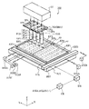
本発明の実施形態を、添付図面に基づいて説明する。図1は、本発明の実施形態にかかる露光装置の構成を概略的に示す図である。本実施形態では、図1に示すように、複数(例示的に4つ)の投影光学系PL1,PL2,PL3,PL4に対してマスクMAおよびプレート(感光性基板)PTを相対移動させつつマスクMAのパターンをプレートPTに投影露光するマルチ走査型の露光装置100に対して本発明を適用している。
Embodiments of the present invention will be described with reference to the accompanying drawings. FIG. 1 is a drawing schematically showing a configuration of an exposure apparatus according to an embodiment of the present invention. In the present embodiment, as shown in FIG. 1, the mask MA and the plate (photosensitive substrate) PT are moved relative to a plurality of (for example, four) projection optical systems PL1, PL2, PL3, and PL4 while moving relative to each other. The present invention is applied to a
本実施形態の露光装置100は、光源からの照明光でマスクMAのパターンを照明する照明装置IUと、マスクMAを保持して移動するマスクステージMST(図1では参照符号だけを示す)と、マスクMAのパターンの拡大像をプレートPT上に投影する投影光学装置PLSと、プレートPTを保持して移動する基板ステージPSTと、マスクステージMST及び基板ステージPSTを駆動するリニアモータ等を含むステージ駆動機構DRと、ステージ駆動機構DR等の動作を統括的に制御する主制御系CRとを備えている。
The
プレートPTは、一例として、液晶表示素子製造用のフォトレジスト(感光材料)が塗布された1.9×2.2m角、2.2×2.4m角、2.4×2.8m角、又は2.8×3.2m角程度の矩形状で平板状のガラスプレートである。また、プレートPTの表面(感光面)は、一例として、マスクMAのパターンがそれぞれ転写される2つのパターン転写領域EP1,EP2に区分して主制御系CRに認識される。 As an example, the plate PT is a 1.9 × 2.2 m square, 2.2 × 2.4 m square, 2.4 × 2.8 m square coated with a photoresist (photosensitive material) for manufacturing a liquid crystal display element, Or it is a rectangular and flat glass plate of about 2.8 × 3.2 m square. Further, as an example, the surface (photosensitive surface) of the plate PT is recognized by the main control system CR by dividing it into two pattern transfer areas EP1 and EP2 to which the pattern of the mask MA is transferred.
以下、説明を容易するために、図1において、基板ステージPSTのガイド面(不図示)に垂直な方向にZ軸を、そのガイド面に平行な面内で走査露光時のプレートPTの走査方向に沿ってX軸を、ガイド面に平行な面内でX軸と直交する非走査方向に沿ってY軸を設定する。また、説明を容易するために、4つの投影光学系PL1〜PL4は互いに同じ構成を有し、区別しない場合には参照符号PLで表すものとする。本実施形態では、基板ステージPSTのガイド面は、マスクステージMSTのガイド面(不図示)に平行であり、走査露光時のマスクMAの走査方向はX軸に平行である。また、Z軸に平行な軸回りの回転方向をθz方向とも呼ぶ。 Hereinafter, for ease of explanation, in FIG. 1, the scanning direction of the plate PT at the time of scanning exposure in the direction perpendicular to the guide surface (not shown) of the substrate stage PST in the direction parallel to the guide surface. Along the non-scanning direction perpendicular to the X axis in a plane parallel to the guide surface. For ease of explanation, the four projection optical systems PL1 to PL4 have the same configuration as each other, and are denoted by the reference symbol PL when not distinguished from each other. In the present embodiment, the guide surface of the substrate stage PST is parallel to the guide surface (not shown) of the mask stage MST, and the scanning direction of the mask MA during scanning exposure is parallel to the X axis. A rotation direction around an axis parallel to the Z axis is also referred to as a θz direction.
照明装置IUでは、例えば光源部の4つ(投影光学系と同数)の送光部から、露光用の照明光(露光光)が射出される。露光光として、超高圧水銀ランプの射出光から選択されたi線(波長365nm)の光が使用されている。なお、露光光として、例えばYAGレーザの3倍高調波(波長355nm)よりなるパルス光、超高圧水銀ランプから射出されるg線(波長436nm)、h線(波長405nm)及びi線(波長365nm)の光を含む波長域から選択された波長の光、又はKrF(波長248nm)若しくはArF(波長193nm)等のエキシマレーザ光等も使用可能である。 In the illumination device IU, for example, illumination light (exposure light) for exposure is emitted from four (same number as the projection optical system) light transmission units of the light source unit. As the exposure light, light of i-line (wavelength 365 nm) selected from the light emitted from the ultra-high pressure mercury lamp is used. As the exposure light, for example, pulsed light composed of a third harmonic (wavelength 355 nm) of a YAG laser, g-line (wavelength 436 nm), h-line (wavelength 405 nm) and i-line (wavelength 365 nm) emitted from an ultrahigh pressure mercury lamp. ) Light having a wavelength selected from a wavelength region including light, or excimer laser light such as KrF (wavelength 248 nm) or ArF (wavelength 193 nm) can also be used.
4つの送光部から射出された照明光は、対応する4つの部分照明光学系(不図示)を介して、マスクMA上においてY方向に沿って間隔を隔てて一列に配置された4つの台形状の照明領域(照野領域)IF1,IF2,IF3,IF4をほぼ均一に照明する。各部分照明光学系は、例えば、コリメータレンズ、フライアイレンズ、集光レンズ、可変視野絞り、リレー光学系などを備えている。 The illumination light emitted from the four light transmission units is arranged in four rows on the mask MA at intervals along the Y direction via corresponding four partial illumination optical systems (not shown). The illumination areas (illumination field areas) IF1, IF2, IF3, and IF4 are illuminated substantially uniformly. Each partial illumination optical system includes, for example, a collimator lens, a fly-eye lens, a condenser lens, a variable field stop, a relay optical system, and the like.
マスクMAの照明領域IF1〜IF4からの光は、対応する4つの投影光学系PL1〜PL4を介して、プレートPT上の台形状の露光領域(像野領域又はイメージフィールド)EF1,EF2,EF3,EF4を露光する。投影光学系PL1〜PL4は、それぞれマスクMA側及びプレートPT側にテレセントリックであり、マスクMA側からプレートPT側へ拡大倍率を有する。露光領域EF1〜EF4の形状は、照明領域IF1〜IF4の形状を投影光学系PL1〜PL4の投影倍率で拡大した形状である。投影光学系PL1〜PL4及びこれらに対応する露光領域EF1〜EF4はY方向に間隔を隔てて一列に配置されている。 Light from the illumination areas IF1 to IF4 of the mask MA passes through corresponding four projection optical systems PL1 to PL4, and trapezoidal exposure areas (image field areas or image fields) EF1, EF2, EF3 on the plate PT. EF4 is exposed. The projection optical systems PL1 to PL4 are telecentric on the mask MA side and the plate PT side, respectively, and have an enlargement magnification from the mask MA side to the plate PT side. The shapes of the exposure regions EF1 to EF4 are shapes obtained by enlarging the shapes of the illumination regions IF1 to IF4 with the projection magnification of the projection optical systems PL1 to PL4. The projection optical systems PL1 to PL4 and the exposure areas EF1 to EF4 corresponding to these are arranged in a line at intervals in the Y direction.
本実施形態では、4つの投影光学系PL1〜PL4を含んで投影光学装置PLSが構成され、各投影光学系PL1〜PL4は、それぞれマスクMA上の照明領域IF1〜IF4内のパターンを共通の拡大倍率βで拡大した投影像を、プレートPTの表面上の露光領域EF1〜EF4に形成する。投影光学系PL1〜PL4は、マスクMAのパターンのX方向(走査方向)およびY方向(非走査方向)に倒立像を、プレートPT上に形成する。 In the present embodiment, the projection optical apparatus PLS is configured to include four projection optical systems PL1 to PL4, and the projection optical systems PL1 to PL4 respectively enlarge the patterns in the illumination areas IF1 to IF4 on the mask MA in common. Projection images enlarged at a magnification β are formed in the exposure regions EF1 to EF4 on the surface of the plate PT. The projection optical systems PL1 to PL4 form inverted images on the plate PT in the X direction (scanning direction) and the Y direction (non-scanning direction) of the pattern of the mask MA.
マスクMAは、マスクホルダ(不図示)を介して、マスクステージMST上に吸着保持されている。マスクステージMST上にはX軸の移動鏡およびY軸の移動鏡が固定され、これらの移動鏡に対向するようにX軸のレーザ干渉計及びY軸のレーザ干渉計よりなるマスク側レーザ干渉計が配置されている。マスク側レーザ干渉計は、マスクステージMSTのX方向、Y方向の位置、及びマスクステージMSTのθz方向の回転角を計測し、計測結果を主制御系CRに供給する。主制御系CRは、その計測値に基づいてリニアモータ等のステージ駆動機構DRを介して、マスクステージMSTのX方向、Y方向の位置及び速度、並びにθz方向の回転角を制御する。 Mask MA is sucked and held on mask stage MST via a mask holder (not shown). An X-axis movable mirror and a Y-axis movable mirror are fixed on the mask stage MST, and a mask-side laser interferometer comprising an X-axis laser interferometer and a Y-axis laser interferometer so as to face these movable mirrors. Is arranged. The mask side laser interferometer measures the X- and Y-direction positions of the mask stage MST and the rotation angle of the mask stage MST in the θz direction, and supplies the measurement results to the main control system CR. The main control system CR controls the position and speed of the mask stage MST in the X and Y directions and the rotation angle in the θz direction via a stage drive mechanism DR such as a linear motor based on the measured values.
プレートPTは、基板ホルダ(不図示)を介して、基板ステージPST上に吸着保持されている。基板ステージPSTにはX軸の移動鏡51X及びY軸の移動鏡51Yが固定され、X軸の移動鏡51Xに対向するように計測用レーザビームをX軸に平行に照射するレーザ干渉計21XA,21XB,21XC及び補助レーザ干渉計21XDが配置されている。また、Y軸の移動鏡51Yに対向するように、計測用レーザビームをY軸に平行に照射するレーザ干渉計21YA及び補助レーザ干渉計21YBが配置されている。
The plate PT is sucked and held on the substrate stage PST via a substrate holder (not shown). An
X軸のレーザ干渉計21XC及びY軸のレーザ干渉計21YAによって基板ステージPSTのX方向及びY方向の位置が計測され、X軸の両側のレーザ干渉計21XA,21XBによって走査露光時の基板ステージPSTのθz方向の回転角が計測される。また、Y軸のレーザ干渉計21YA及び補助レーザ干渉計21YBによって、基板ステージPSTがY方向にステップ移動する際の、基板ステージPSTのθz方向の回転角が計測される。なお、例えば移動鏡51X,51Yの真直度が良好である場合等には、X軸のレーザ干渉計21XA〜21XDのうちの2つのレーザ干渉計(例えば21XA,21XB)を設けるのみでもよく、Y軸の補助レーザ干渉計21YBは省略可能である。
The X-axis and Y-direction positions of the substrate stage PST are measured by the X-axis laser interferometer 21XC and the Y-axis laser interferometer 21YA, and the substrate stage PST at the time of scanning exposure is measured by the laser interferometers 21XA and 21XB on both sides of the X-axis. The rotation angle in the θz direction is measured. Further, the rotation angle in the θz direction of the substrate stage PST when the substrate stage PST is stepped in the Y direction is measured by the Y-axis laser interferometer 21YA and the auxiliary laser interferometer 21YB. For example, when the straightness of the
これらのレーザ干渉計21XA〜21XD,21YA,21YBよりなるプレート側レーザ干渉計の計測値は、主制御系CRに供給される。主制御系CRは、その計測値に基づいてリニアモータ等のステージ駆動機構DRを介して、基板ステージPSTのX方向、Y方向の位置及び速度を制御する。走査露光時には、マスクステージMSTがX方向に速度V/βで駆動されるのに同期して、基板ステージPSTはX方向に速度Vで駆動される。投影光学系PL1〜PL4の像はX方向に倒立像であるため、マスクステージMSTの走査方向と基板ステージPSTの走査方向とはX軸に沿って逆向きになる。また、Y方向にも倒立像であるため、マスクMA上のパターンとプレートPT上に形成されるパターンとは、X方向およびY方向に逆向きとなる。 The measurement values of the plate side laser interferometer composed of these laser interferometers 21XA to 21XD, 21YA, and 21YB are supplied to the main control system CR. The main control system CR controls the position and speed of the substrate stage PST in the X and Y directions via a stage drive mechanism DR such as a linear motor based on the measured values. At the time of scanning exposure, the substrate stage PST is driven at the speed V in the X direction in synchronization with the mask stage MST being driven at the speed V / β in the X direction. Since the images of the projection optical systems PL1 to PL4 are inverted in the X direction, the scanning direction of the mask stage MST and the scanning direction of the substrate stage PST are opposite to each other along the X axis. Further, since the image is also an inverted image in the Y direction, the pattern on the mask MA and the pattern formed on the plate PT are opposite in the X direction and the Y direction.
投影光学系PL1〜PL4の近傍には、プレートPTの位置合わせを行うための例えば画像処理方式のオフアクシス型のアライメント系ALG、並びにマスクMA及びプレートPTのZ方向の位置(フォーカス位置)を計測するオートフォーカス系(不図示)が配置されている。そのため、プレートPT上のパターン転写領域EP1及びEP2の近傍には、それぞれ複数のアライメントマークAM1及びAM2が形成されている。また、そのオートフォーカス系の計測結果に基づいて、ステージ駆動機構DR内のZ駆動機構を用いて例えばマスクステージMSTのZ方向の位置の制御、及び/又は投影光学系PL1〜PL4の個別のフォーカス機構(不図示)を駆動することによって、投影光学系PL1〜PL4の像面とプレートPTの表面との合焦が行われる。 In the vicinity of the projection optical systems PL1 to PL4, for example, an image processing type off-axis alignment system ALG for aligning the plate PT, and the position in the Z direction (focus position) of the mask MA and the plate PT are measured. An autofocus system (not shown) is arranged. Therefore, a plurality of alignment marks AM1 and AM2 are formed in the vicinity of the pattern transfer regions EP1 and EP2 on the plate PT, respectively. Further, based on the measurement result of the autofocus system, for example, control of the position of the mask stage MST in the Z direction and / or individual focus of the projection optical systems PL1 to PL4 using the Z drive mechanism in the stage drive mechanism DR. By driving a mechanism (not shown), the image planes of the projection optical systems PL1 to PL4 and the surface of the plate PT are focused.
また、基板ステージPSTには、投影光学系PL1〜PL4を介して投影されるマスクMA上の位置計測用マークの像の位置を計測するためのアライメント系として、空間像計測系53が設置されている。アライメント系ALG及び空間像計測系53の検出信号はアライメント信号処理系(不図示)で処理され、この処理によって得られた被検マークの位置情報が主制御系CRに供給される。
The substrate stage PST is provided with an aerial
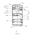
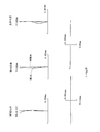
図2は、本実施形態にかかる投影光学系の基本構成を模式的に示す図である。図2を参照すると、本実施形態の投影光学系PLは、マスクMAのパターン面(第1面)の照明領域(第1領域)IFのパターンの像をプレートPTの表面(第2面)の露光領域(第2領域)EFに形成する反射屈折光学系である。投影光学系PLは、正の屈折力を有する第1レンズ群G1と、第1レンズ群G1を介した照明領域IFからの光をマスクMA側に反射する曲面状の反射面CMaと、曲面状の反射面CMaが反射した光をプレートPT側に反射する平面状の反射面FMaと、正の屈折力を有し、平面状の反射面FMaが反射した光を露光領域EFに集光する第2レンズ群G2とを備えている。 FIG. 2 is a diagram schematically showing the basic configuration of the projection optical system according to the present embodiment. Referring to FIG. 2, the projection optical system PL of the present embodiment converts an image of the pattern of the illumination area (first area) IF of the pattern surface (first surface) of the mask MA onto the surface (second surface) of the plate PT. This is a catadioptric optical system formed in the exposure area (second area) EF. The projection optical system PL includes a first lens group G1 having a positive refractive power, a curved reflecting surface CMa that reflects light from the illumination area IF via the first lens group G1 toward the mask MA, and a curved surface. A planar reflecting surface FMa that reflects the light reflected by the reflecting surface CMa toward the plate PT side, and a first light that has positive refractive power and that reflects the light reflected by the planar reflecting surface FMa in the exposure area EF. 2 lens group G2.
第1レンズ群G1、第2レンズ群G2及び曲面状の反射面CMa(ひいては曲面状の反射面CMaを有する曲面反射鏡CM)は直線状の1本の光軸AXに沿って共軸に配置され、平面状の反射面FMa(ひいては平面状の反射面FMaを有する平面反射鏡FM)は光軸AXに対して偏心配置されている。ここで、偏心配置されているとは、光軸AXと交差しない位置に配置されていることを意味する。なお、曲面状の反射面CMaは、投影光学系PLの射出瞳(もしくは入射瞳)と共役な面の近傍に配置されており、この曲面状の反射面CMa(ひいては曲面状の反射面CMaが設けられた反射部材)は、開口絞りとして作用する。 The first lens group G1, the second lens group G2, and the curved reflecting surface CMa (and thus the curved reflecting mirror CM having the curved reflecting surface CMa) are arranged coaxially along one linear optical axis AX. The planar reflecting surface FMa (and thus the planar reflecting mirror FM having the planar reflecting surface FMa) is eccentrically arranged with respect to the optical axis AX. Here, being arranged eccentrically means being arranged at a position that does not intersect the optical axis AX. The curved reflection surface CMa is disposed in the vicinity of a surface conjugate with the exit pupil (or entrance pupil) of the projection optical system PL, and this curved reflection surface CMa (and thus the curved reflection surface CMa is the same). The reflection member provided acts as an aperture stop.
本実施形態の投影光学系PLでは、屈折力(またはパワー)を有するすべての光学部材が1つの鏡筒VA内で直線状の1本の光軸AXに沿って共軸に配置されるので、1本鏡筒タイプの屈折光学系と同様に光学系の組立て調整が容易であり、偏心収差の発生を良好に抑えることができる。また、本実施形態の投影光学系PLは反射屈折光学系の形態を有するので、レンズ枚数等を抑えたコンパクトな構成で収差を良好に補正することができる。すなわち、本実施形態では、レンズ枚数等を抑えたコンパクトな構成を有し、組立て調整を容易に行うことのできる反射屈折型の投影光学系を実現することができる。 In the projection optical system PL of the present embodiment, all optical members having refractive power (or power) are arranged coaxially along one linear optical axis AX in one lens barrel VA. As with a single-lens barrel type refractive optical system, the assembly and adjustment of the optical system is easy, and the occurrence of decentration aberrations can be satisfactorily suppressed. In addition, since the projection optical system PL of the present embodiment has the form of a catadioptric optical system, it is possible to correct aberrations favorably with a compact configuration with a reduced number of lenses. That is, in the present embodiment, it is possible to realize a catadioptric projection optical system that has a compact configuration with a reduced number of lenses and the like and can be easily adjusted in assembly.
なお、本実施形態の投影光学系PLでは、平面状の反射面FMaが光軸AXに対して偏心配置されるが、反射面FMaはパワーを有しないため、例えばX方向に反射面FMaの位置決め誤差が発生しても、この位置決め誤差に起因して偏心収差が発生することはない。これに対して、例えば第2の曲面反射鏡が光軸に対して偏心配置される従来の反射屈折光学系では、パターン面からの光の光路を確保する必要性(光路分離の必要性)から半欠け形状になる第2の曲面反射鏡の光軸に対する位置決め(ひいては光学系の組立て調整)が困難であり、第2の曲面反射鏡の位置決め誤差に起因して偏心収差が発生し易い。 In the projection optical system PL of the present embodiment, the planar reflecting surface FMa is eccentrically arranged with respect to the optical axis AX. However, since the reflecting surface FMa has no power, for example, the reflecting surface FMa is positioned in the X direction. Even if an error occurs, no decentration aberration occurs due to this positioning error. On the other hand, for example, in a conventional catadioptric optical system in which the second curved reflector is arranged eccentrically with respect to the optical axis, it is necessary to secure an optical path of light from the pattern surface (necessity of optical path separation). It is difficult to position the second curved reflecting mirror having a semi-chip shape with respect to the optical axis (and consequently assembly adjustment of the optical system), and decentration aberrations are likely to occur due to positioning errors of the second curved reflecting mirror.
後述する各実施例では、曲面状の反射面CMaは、マスクMA側に凹面状の反射面である。すなわち、各実施例において、曲面反射鏡CMは、凹面反射鏡である。また、各実施例において、平面状の反射面FMaは、光軸AXに対して垂直に配置されている。また、各実施例において、投影光学系PLは、マスクMAの台形状の照明領域IFのパターンの拡大像をプレートPTの台形状の露光領域EFに形成する。 In each embodiment described later, the curved reflecting surface CMa is a concave reflecting surface on the mask MA side. That is, in each embodiment, the curved reflecting mirror CM is a concave reflecting mirror. In each embodiment, the planar reflecting surface FMa is arranged perpendicular to the optical axis AX. In each embodiment, the projection optical system PL forms an enlarged image of the pattern of the trapezoidal illumination area IF of the mask MA in the trapezoidal exposure area EF of the plate PT.
本発明の投影光学系は、1.5〜3倍の拡大投影に好適である。すなわち、拡大倍率βについて、次の条件式(1)を満足することが好ましい。
1.5<β<3 (1)
The projection optical system of the present invention is suitable for magnification projection of 1.5 to 3 times. That is, it is preferable that the following conditional expression (1) is satisfied for the magnification β.
1.5 <β <3 (1)
条件式(1)の上限値を上回ると、第1レンズ群G1の焦点距離が短くなり屈折力が強くなるために、曲面反射鏡CMへの光の入射角が大きくなり、瞳収差や像面湾曲が大きくなる等のデメリットが生じる。逆に、条件式(1)の下限値を下回ると、投影倍率が等倍(1倍)に近くなるので収差補正上は有利になるが、投影像を拡大する効果が抑制される。このため、露光装置100においてマスクMAの大型化を抑制する効果が低減される。
If the upper limit of conditional expression (1) is exceeded, the focal length of the first lens group G1 is shortened and the refractive power is increased, so that the incident angle of light to the curved reflector CM is increased, and pupil aberration and image plane are increased. Demerits such as an increase in curvature occur. On the other hand, if the lower limit value of conditional expression (1) is not reached, the projection magnification becomes close to the same magnification (1 time), which is advantageous in terms of aberration correction, but the effect of enlarging the projected image is suppressed. For this reason, the effect of suppressing the enlargement of the mask MA in the
本実施形態の投影光学系PLでは、第1レンズ群G1の焦点距離をfとし、曲面状の反射面CMaと平面状の反射面FMaとの間の光軸AXに沿った距離をdmとするとき、次の条件式(2)を満足することが好ましい。
0.7<dm/f<1 (2)
In the projection optical system PL of this embodiment, the focal length of the first lens group G1 is f, the distance along the optical axis AX between the curved reflecting surfaces CMa a planar reflecting surface FMa and d m It is preferable that the following conditional expression (2) is satisfied.
0.7 <d m / f <1 (2)
条件式(2)の上限値を上回ると、平面状の反射面FMaから第2レンズ群G2へ向かう光束と曲面反射鏡CMとの干渉を回避することは容易になるが、曲面反射鏡CMへの光の入射角度が大きくなり、瞳収差が大きくなる等のデメリットが生じる。逆に、条件式(2)の下限値を下回ると、曲面反射鏡CMへの光の入射角度が小さくなるので収差補正上は有利になるが、平面状の反射面FMaから第2レンズ群G2へ向かう光束と曲面反射鏡CMとの干渉を回避することが困難になる。なお、曲面反射鏡CMの光路干渉を回避しつつ良好な収差補正を行うには、条件式(2)の下限値を0.9に設定することがさらに好ましい。 If the upper limit value of conditional expression (2) is exceeded, it is easy to avoid interference between the light beam traveling from the planar reflecting surface FMa toward the second lens group G2 and the curved reflecting mirror CM, but to the curved reflecting mirror CM. The incident angle of the light increases, and disadvantages such as an increase in pupil aberration occur. On the contrary, if the lower limit of conditional expression (2) is not reached, the incident angle of light to the curved reflecting mirror CM becomes small, which is advantageous in terms of aberration correction, but from the planar reflecting surface FMa to the second lens group G2. It becomes difficult to avoid the interference between the light beam traveling toward the curved surface and the curved reflecting mirror CM. In order to perform good aberration correction while avoiding optical path interference of the curved reflector CM, it is more preferable to set the lower limit value of conditional expression (2) to 0.9.
また、本実施形態では、第1レンズ群G1は、マスクMAの照明領域IFからの光の入射順に、負レンズ群G1nと、正レンズ群G1pとを備えていることが好ましい。この構成により、主に像面湾曲の補正が有利になるとともに、平面状の反射面FMaを含む平面に入射する光線の光軸AXからの高さを大きくすることができる。その結果、第1レンズ群G1から曲面状の反射面CMaへの入射光束と平面状の反射面FMaとの干渉を回避することが容易となり、ひいては視野(露光領域)を広げ易くなる。また、第1レンズ群G1が光の入射順に負レンズ群G1nと正レンズ群G1pとを備え、いわゆるレトロタイプの配置を採る場合、条件式(2)を満足することにより、第1レンズ群G1のプレートPT側の面と平面状の反射面FMaとの干渉を回避することが容易になる。 In the present embodiment, the first lens group G1 preferably includes a negative lens group G1n and a positive lens group G1p in the order of incidence of light from the illumination area IF of the mask MA. With this configuration, correction of curvature of field is mainly advantageous, and the height of the light beam incident on the plane including the planar reflection surface FMa can be increased. As a result, it becomes easy to avoid interference between the incident light beam from the first lens group G1 to the curved reflecting surface CMa and the planar reflecting surface FMa, and it is easy to widen the field of view (exposure region). Further, when the first lens group G1 includes a negative lens group G1n and a positive lens group G1p in the order of incidence of light and adopts a so-called retrotype arrangement, the first lens group G1 is satisfied by satisfying conditional expression (2). It is easy to avoid interference between the surface on the plate PT side and the planar reflecting surface FMa.
第1レンズ群G1が、光の入射順に、負レンズ群G1nと正レンズ群G1pとを備える場合、第1レンズ群G1の焦点距離をfとし、負レンズ群G1nの焦点距離をf1とし、正レンズ群G1pの焦点距離をf2とするとき、次の条件式(3)を満足することが好ましい。
0.5<(|f1|/f2)/(f/(f−f2))<1 (3)
When the first lens group G1 includes the negative lens group G1n and the positive lens group G1p in the light incident order, the focal length of the first lens group G1 is f, the focal length of the negative lens group G1n is f1, When the focal length of the lens group G1p is f2, it is preferable that the following conditional expression (3) is satisfied.
0.5 <(| f1 | / f2) / (f / (f−f2)) <1 (3)
条件式(3)の上限値を上回ると、負レンズ群G1nの屈折力が弱くなり過ぎて、像面湾曲を良好に補正することが困難になる。また、第1レンズ群G1からの光の光路と平面状の反射面FMaとの分離が困難になって、視野を狭くする必要が生じる。一方、条件式(3)の下限値を下回ると、負レンズ群G1nの屈折力が強くなり過ぎて、像面湾曲、ディストーション(歪曲収差)等の像高に応じた収差が悪化する。その結果、これらの収差を抑えるために負レンズ群G1nと正レンズ群G1pとの間隔を大きくせざるを得なくなり、投影光学系の全長が大きくなってしまう。 If the upper limit of conditional expression (3) is exceeded, the refractive power of the negative lens group G1n becomes too weak, and it becomes difficult to correct the field curvature well. In addition, it becomes difficult to separate the optical path of light from the first lens group G1 and the planar reflecting surface FMa, and the field of view needs to be narrowed. On the other hand, if the lower limit of conditional expression (3) is not reached, the refractive power of the negative lens group G1n becomes too strong, and aberrations according to image height such as field curvature and distortion (distortion aberration) deteriorate. As a result, in order to suppress these aberrations, the distance between the negative lens group G1n and the positive lens group G1p must be increased, and the overall length of the projection optical system is increased.
また、本実施形態の投影光学系PLは、曲面状の反射面CMaと平面状の反射面FMaとの間で光軸AXに沿って曲面状の反射面CMaと共軸に配置され、曲面状の反射面CMa側の端部に負レンズLnを有する第3レンズ群G3を備えることが好ましい。この構成により、光学系の全体的な屈折力配分を容易に行うことができる。なお、負レンズLnを曲面状の反射面CMaの近傍に配置することにより、主に色収差の補正および球面収差の補正を有効に行うことができる。 In addition, the projection optical system PL of the present embodiment is disposed between the curved reflecting surface CMa and the planar reflecting surface FMa along the optical axis AX and coaxially with the curved reflecting surface CMa. It is preferable to include a third lens group G3 having a negative lens Ln at the end of the reflecting surface CMa. With this configuration, the overall refractive power distribution of the optical system can be easily performed. By disposing the negative lens Ln in the vicinity of the curved reflecting surface CMa, mainly correction of chromatic aberration and correction of spherical aberration can be effectively performed.
また、マスクMAの照明領域IFからの光は負レンズLnを介して曲面状の反射面CMaに入射し、曲面状の反射面CMaによって反射された光は負レンズLnを介して平面状の反射面FMaに入射し、平面状の反射面FMaによって反射された光は負レンズLnを介して第2レンズ群G2に入射する。このように、マスクMAの照明領域IFからの光がプレートPTの露光領域EFに達するまでに、負レンズLnを含む第3レンズ群G3を3回通過するので、第3レンズ群G3を構成する各レンズの屈折力を有効に利用して、光学系全体のレンズ枚数を少なく抑えることが可能になる。 The light from the illumination area IF of the mask MA is incident on the curved reflecting surface CMa via the negative lens Ln, and the light reflected by the curved reflecting surface CMa is planarly reflected via the negative lens Ln. The light incident on the surface FMa and reflected by the planar reflecting surface FMa enters the second lens group G2 via the negative lens Ln. In this way, the third lens group G3 is formed because the light from the illumination area IF of the mask MA passes through the third lens group G3 including the negative lens Ln three times before reaching the exposure area EF of the plate PT. By effectively using the refractive power of each lens, it is possible to reduce the number of lenses in the entire optical system.
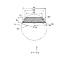
以下に示す各実施例において、プレートPTの表面には、図3に示すように、光軸AXを中心とする半径Raの円31と光軸AXから+X方向に距離Rbだけ間隔を隔ててY方向に延びる直線32とにより規定される有効結像領域33が確保される。ここで、「有効結像領域」とは、投影光学系PLの像面において収差が所望の状態に補正された領域を意味している。したがって、照明装置IU内の可変視野絞りの作用により、底辺の長さがLaで、上辺の長さがLbで、高さがLcの台形状の露光領域EFが、有効結像領域33内に設定される。各実施例では、半径Ra(すなわち最大像高)が142mmであり、距離Rbが85mmであり、底辺の長さLaが226mmであり、上辺の長さLbが190mmであり、高さLcが20mmである。そして、マスクMAのパターン面には、光軸AXから間隔を隔てた台形状の露光領域EFに対応するように、光軸AXから間隔を隔てた台形状の照明領域IF(不図示)が形成される。
In each of the embodiments described below, the surface of the plate PT is provided with a
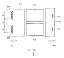
すなわち、図4に示すように、第2投影光学系PL2に対応して、プレートPTの感光面には台形状の露光領域EF2が形成され、マスクMAのパターン面には台形状の照明領域IF2が形成される。同様に、第2投影光学系PL2からY方向に間隔を隔てて配置された第3投影光学系PL3に対応して、プレートPTの感光面には台形状の露光領域EF3が形成され、マスクMAのパターン面には台形状の照明領域IF3が形成される。図4では、第2投影光学系PL2および第3投影光学系PL3に対応する露光領域および照明領域だけを示しているが、他の投影光学系PL1,PL4についても同様である。また、図4では、説明の理解を容易にするために、マスクMAと投影光学系PLとプレートPTとが重なり合わないようにX方向に沿って互いに位置ずれさせている。 That is, as shown in FIG. 4, a trapezoidal exposure area EF2 is formed on the photosensitive surface of the plate PT corresponding to the second projection optical system PL2, and a trapezoidal illumination area IF2 is formed on the pattern surface of the mask MA. Is formed. Similarly, a trapezoidal exposure area EF3 is formed on the photosensitive surface of the plate PT corresponding to the third projection optical system PL3 arranged at a distance in the Y direction from the second projection optical system PL2, and the mask MA A trapezoidal illumination area IF3 is formed on the pattern surface. FIG. 4 shows only the exposure area and the illumination area corresponding to the second projection optical system PL2 and the third projection optical system PL3, but the same applies to the other projection optical systems PL1 and PL4. In FIG. 4, in order to facilitate understanding of the description, the mask MA, the projection optical system PL, and the plate PT are displaced from each other along the X direction so as not to overlap.
以下、説明を簡単にするために、各露光領域の形状および大きさは互いに同じであり、各露光領域の一対の斜辺の中点を結ぶ線分と隣り合う2つの露光領域の対向する斜辺の中点を結ぶ線分とは互いに同じ長さLd(図3も参照:各実施例ではLd=208mm)に設定されているものとする。この場合、マスクMAを矢印MDで示すように+X方向に移動させ且つプレートPTを矢印PDで示すように−X方向に移動させる1回目の走査露光により、例えば第1転写領域EP1の約半分の領域の投影露光が行われる。次いで、プレートPTをY方向に距離Ldだけステップ移動させた後、マスクMAを矢印MDで示す方向とは逆方向の−X方向に移動させ且つプレートPTを矢印PDで示す方向とは逆方向の+X方向に移動させる2回目の走査露光により、第1転写領域EP1の残りの領域の投影露光が行われる。なお、各露光領域の形状、大きさ、配置などについては、様々な変形例が可能である。以下、各実施例の詳細について説明する。 Hereinafter, in order to simplify the description, the shape and size of each exposure area are the same, and the opposite hypotenuses of two adjacent exposure areas are adjacent to the line segment connecting the midpoints of the pair of hypotenuses of each exposure area. The line segments connecting the midpoints are set to the same length Ld (see also FIG. 3; Ld = 208 mm in each embodiment). In this case, by the first scanning exposure in which the mask MA is moved in the + X direction as indicated by the arrow MD and the plate PT is moved in the −X direction as indicated by the arrow PD, for example, about half of the first transfer region EP1 is obtained. Area projection exposure is performed. Next, after the plate PT is moved stepwise in the Y direction by a distance Ld, the mask MA is moved in the −X direction opposite to the direction indicated by the arrow MD and the plate PT is moved in the direction opposite to the direction indicated by the arrow PD. Projection exposure of the remaining area of the first transfer area EP1 is performed by the second scanning exposure moved in the + X direction. Various modifications can be made to the shape, size, arrangement, etc. of each exposure region. Details of each embodiment will be described below.
各実施例において、非球面は、光軸に垂直な方向の高さをyとし、非球面の頂点における接平面から高さyにおける非球面上の位置までの光軸に沿った距離(サグ量)をzとし、頂点曲率半径をrとし、円錐係数をκとし、n次の非球面係数をCnとしたとき、以下の数式(a)で表される。後述の表(1)および(2)において、非球面形状に形成されたレンズ面には面番号の右側に*印を付している。
z=(y2/r)/[1+{1−(1+κ)・y2/r2}1/2]+C4・y4+C6・y6
+C8・y8+C10・y10+C12・y12+C14・y14 (a)
In each embodiment, the height of the aspheric surface in the direction perpendicular to the optical axis is y, and the distance (sag amount) along the optical axis from the tangential plane at the apex of the aspheric surface to the position on the aspheric surface at height y. ) Is z, the apex radius of curvature is r, the conic coefficient is κ, and the nth-order aspheric coefficient is C n , it is expressed by the following formula (a). In Tables (1) and (2), which will be described later, an aspherical lens surface is marked with an asterisk (*) on the right side of the surface number.
z = (y 2 / r) / [1+ {1− (1 + κ) · y 2 / r 2 } 1/2 ] + C 4 · y 4 + C 6 · y 6
+ C 8 · y 8 + C 10 · y 10 + C 12 · y 12 + C 14 · y 14 (a)
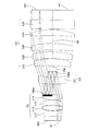
[第1実施例]
図5は、本実施形態の第1実施例にかかる投影光学系のレンズ構成を示す図である。第1実施例の投影光学系PLにおいて、第1レンズ群G1は、マスクMAの台形状の照明領域IFからの光の入射順に、負レンズL11と、3つの正レンズL12、L13およびL14とにより構成されている。第3レンズ群G3は、第1レンズ群G1からの光の入射順に、正レンズL31と、負レンズL32とにより構成されている。第2レンズ群G2は、第3レンズ群G3からの光の入射順に、正レンズL21と、負レンズL22と、2つの正レンズL23およびL24と、平行平面板L25とにより構成されている。
[First embodiment]
FIG. 5 is a diagram showing a lens configuration of the projection optical system according to the first example of the present embodiment. In the projection optical system PL of the first example, the first lens group G1 includes a negative lens L11 and three positive lenses L12, L13, and L14 in the order of incidence of light from the trapezoidal illumination area IF of the mask MA. It is configured. The third lens group G3 includes a positive lens L31 and a negative lens L32 in the order of incidence of light from the first lens group G1. The second lens group G2 includes a positive lens L21, a negative lens L22, two positive lenses L23 and L24, and a plane parallel plate L25 in the order of incidence of light from the third lens group G3.
第1実施例では、平面状の反射面FMaが平面反射鏡FMの反射面として構成され、曲面状の反射面CMaが凹面反射鏡CMの反射面として構成されている。第1レンズ群G1において、負レンズL11が負レンズ群G1nを構成し、3つの正レンズL12、L13およびL14が正レンズ群G1pを構成している。第3レンズ群G3において、負レンズL32が、第3レンズ群G3の端部において曲面状の反射面CMaの近傍に配置される負レンズを構成している。また、凹面反射鏡CMの曲面状の反射面CMaが、開口絞りとして作用している。 In the first embodiment, the planar reflecting surface FMa is configured as the reflecting surface of the planar reflecting mirror FM, and the curved reflecting surface CMa is configured as the reflecting surface of the concave reflecting mirror CM. In the first lens group G1, the negative lens L11 forms a negative lens group G1n, and the three positive lenses L12, L13, and L14 form a positive lens group G1p. In the third lens group G3, the negative lens L32 constitutes a negative lens disposed in the vicinity of the curved reflecting surface CMa at the end of the third lens group G3. The curved reflecting surface CMa of the concave reflecting mirror CM acts as an aperture stop.
第1実施例では、マスクMAの台形状の照明領域IFからの光が、第1レンズ群G1および第3レンズ群G3を順次経て凹面反射鏡CMの曲面状の反射面CMaによって反射され、第3レンズ群G3を経て、平面反射鏡FMの反射面FMaによって反射される。平面反射鏡FMによって反射された光は、第3レンズ群G3および第2レンズ群G2を順次経た後に、プレートPTの台形状の露光領域EFに、照明領域IF内のパターンの拡大像を形成する。 In the first example, the light from the trapezoidal illumination area IF of the mask MA is reflected by the curved reflecting surface CMa of the concave reflecting mirror CM through the first lens group G1 and the third lens group G3 in order. The light is reflected by the reflecting surface FMa of the plane reflecting mirror FM through the three lens groups G3. The light reflected by the plane reflecting mirror FM sequentially passes through the third lens group G3 and the second lens group G2, and then forms an enlarged image of the pattern in the illumination area IF in the trapezoidal exposure area EF of the plate PT. .
次の表(1)に、第1実施例にかかる投影光学系PLの諸元の値を掲げる。表(1)の主要諸元において、λは露光光の中心波長を、βは投影光学系PLのマスクMAからプレートPTへの投影倍率の大きさ(絶対値)を、NAは像側(プレートPT側)開口数をそれぞれ表している。また、表(1)の光学部材諸元において、面番号は光の入射側からの面の順序を、rは各面の曲率半径(非球面の場合には頂点曲率半径:mm)を、dは各面の軸上間隔すなわち当該面から次の面までの光軸に沿った間隔(mm)を、nは中心波長に対する媒質の屈折率をそれぞれ示している。なお、面間隔dおよび屈折率nは、反射される度にその符号を変えるものとする。表(1)における表記は、以降の表(2)においても同様である。 In the following table (1), values of specifications of the projection optical system PL according to the first example are listed. In the main specifications of Table (1), λ is the center wavelength of the exposure light, β is the size (absolute value) of the projection magnification from the mask MA of the projection optical system PL to the plate PT, and NA is the image side (plate (PT side) The numerical aperture is shown respectively. In the optical member specifications of Table (1), the surface number is the order of the surfaces from the light incident side, r is the radius of curvature of each surface (vertical curvature radius: mm in the case of an aspheric surface), d Represents the axial distance between the surfaces, that is, the distance (mm) along the optical axis from the surface to the next surface, and n represents the refractive index of the medium with respect to the center wavelength. Note that the sign of the surface distance d and the refractive index n are changed each time the light is reflected. The notation in Table (1) is the same in the following Table (2).
表(1)
(主要諸元)
λ=365nm
NA=0.054
β=2.5
面番号 r d n 光学部材
物体面 ∞ 22.35362 1
1 -874.40638 28.44099 1.4745570 L11
2* 1260.99850 11.33526 1
3 481.42856 20.00000 1.4876040 L12
4 -597.56435 2.20000 1
5 1602.66850 24.02300 1.4876040 L13
6 -222.34652 2.00000 1
7 -612.86436 20.00000 1.4876040 L14
8 -252.71098 34.10374 1
9* -848.67204 45.00000 1.4745570 L31
10 -701.51462 96.25879 1
11 546.14698 31.79490 1.4745570 L32
12 454.90025 17.46809 1
13 ∞ 0.00000 1 (開口絞り)
14 -466.46853 -17.46809 -1 CM
15 454.90025 -31.79490 -1.4745570 L32
16 546.14698 -96.25879 -1
17 -701.51462 -45.00000 -1.4745570 L31
18* -848.67204 -14.10374 -1
19 ∞ 14.10374 1 FM
20* -848.67204 45.00000 1.4745570 L31
21 -701.51462 96.25879 1
22 546.14698 31.79490 1.4745570 L32
23 454.90025 105.98173 1
24 1212.43910 30.00000 1.4745570 L21
25 17588.05800 3.10848 1
26 559.22273 38.43000 1.4745570 L22
27 446.57657 29.81434 1
28 -9622.13250 30.00000 1.4745570 L23
29 -688.51627 2.20000 1
30 993.96441 41.95512 1.4745570 L24
31 -641.46139 5.00000 1
32 ∞ 50.00000 1.4745570 L25
33 ∞ 72.78173 1
(非球面データ)
2面: κ=0
C4=5.43755×10⁻⁸ C6=−6.95046×10⁻¹³
C8=1.02416×10⁻¹⁶ C10=−4.50830×10⁻²⁰
C12=8.19138×10⁻²⁴ C14=−5.58585×10⁻²⁸
9面(18面および20面と同一面): κ=0
C4=−1.78231×10⁻⁹ C6=6.32794×10⁻¹⁴
C8=2.69771×10⁻¹⁸ C10=−4.84042×10⁻²²
C12=5.70771×10⁻²⁶ C14=−2.67029×10⁻³⁰
(条件式対応値)
dm=204.6mm
f=222.6mm
f1=−1083.4mm
f2=193.3mm
(2)dm/f=0.92
(3)(|f1|/f2)/(f/(f−f2))=0.74
Table (1)
(Main specifications)
λ = 365nm
NA = 0.054
β = 2.5
Surface number rd n Optical member object surface ∞ 22.35362 1
1 -874.40638 28.44099 1.4745570 L11
2 * 1260.99850 11.33526 1
3 481.42856 20.00000 1.4876040 L12
4 -597.56435 2.20000 1
5 1602.66850 24.02300 1.4876040 L13
6 -222.34652 2.00000 1
7 -612.86436 20.00000 1.4876040 L14
8 -252.71098 34.10374 1
9 * -848.67204 45.00000 1.4745570 L31
10 -701.51462 96.25879 1
11 546.14698 31.79490 1.4745570 L32
12 454.90025 17.46809 1
13 ∞ 0.00000 1 (Aperture stop)
14 -466.46853 -17.46809 -1 CM
15 454.90025 -31.79490 -1.4745570 L32
16 546.14698 -96.25879 -1
17 -701.51462 -45.00000 -1.4745570 L31
18 * -848.67204 -14.10374 -1
19 ∞ 14.10374 1 FM
20 * -848.67204 45.00000 1.4745570 L31
21 -701.51462 96.25879 1
22 546.14698 31.79490 1.4745570 L32
23 454.90025 105.98173 1
24 1212.43910 30.00000 1.4745570 L21
25 17588.05800 3.10848 1
26 559.22273 38.43000 1.4745570 L22
27 446.57657 29.81434 1
28 -9622.13250 30.00000 1.4745570 L23
29 -688.51627 2.20000 1
30 993.96441 41.95512 1.4745570 L24
31 -641.46139 5.00000 1
32 ∞ 50.00000 1.4745570 L25
33 ∞ 72.78173 1
(Aspheric data)
Two sides: κ = 0
C 4 = 5.443755 × 10 −8 C 6 = −6.995046 × 10 −13
C 8 = 1.02416 × 10 −16 C 10 = −4.50830 × 10 −20
C 12 = 8.19138 × 10 −24 C 14 = −5.55855 × 10 −28
9 planes (same plane as 18th and 20th planes): κ = 0
C 4 = −1.78231 × 10 −9 C 6 = 6.332794 × 10 −14
C 8 = 2.69771 × 10 −18 C 10 = −4.84042 × 10 −22
C 12 = 5.77071 × 10 −26 C 14 = −2.667029 × 10 −30
(Values for conditional expressions)
d m = 204.6 mm
f = 222.6 mm
f1 = −1083.4 mm
f2 = 193.3mm
(2) d m /f=0.92
(3) (| f1 | / f2) / (f / (f−f2)) = 0.74
図6は、第1実施例の投影光学系における球面収差、像面湾曲、歪曲収差、およびコマ収差を示す図である。収差図において、NAは投影光学系の像側開口数を、Yは像高(mm)を示している。図6の各収差図を参照すると、第1実施例では、台形状の露光領域EFにおいて諸収差が良好に補正されていることがわかる。 FIG. 6 is a diagram showing spherical aberration, curvature of field, distortion, and coma in the projection optical system of the first example. In the aberration diagrams, NA represents the image-side numerical aperture of the projection optical system, and Y represents the image height (mm). Referring to each aberration diagram of FIG. 6, it can be seen that in the first example, various aberrations are satisfactorily corrected in the trapezoidal exposure region EF.
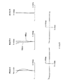
[第2実施例]
図7は、本実施形態の第2実施例にかかる投影光学系のレンズ構成を示す図である。第2実施例の投影光学系PLにおいて、第1レンズ群G1は、マスクMAの台形状の照明領域IFからの光の入射順に、負レンズL11と、3つの正レンズL12、L13およびL14とにより構成されている。第3レンズ群G3は、負レンズL3により構成されている。第2レンズ群G2は、第3レンズ群G3からの光の入射順に、4つの正レンズL21、L22、L23およびL24と、平行平面板L25とにより構成されている。
[Second Embodiment]
FIG. 7 is a diagram showing a lens configuration of the projection optical system according to the second example of the present embodiment. In the projection optical system PL of the second example, the first lens group G1 includes a negative lens L11 and three positive lenses L12, L13, and L14 in the order of incidence of light from the trapezoidal illumination area IF of the mask MA. It is configured. The third lens group G3 includes a negative lens L3. The second lens group G2 includes four positive lenses L21, L22, L23, and L24 and a plane parallel plate L25 in the order of incidence of light from the third lens group G3.
第2実施例では、第1実施例と同様に、曲面状の反射面CMaが凹面反射鏡CMの反射面として構成されている。しかしながら、第1実施例とは異なり、平面状の反射面FMaが、第1レンズ群G1中の平凸レンズL14のプレートPT側の光学面のうち、照明領域IFから第3レンズ群G3への光が通過しない領域に形成されている。すなわち、平面状の反射面FMaは、第1レンズ群G1におけるプレートPT側の端部の光学面の所要領域に形成されている。また、第1レンズ群G1において、負レンズL11が負レンズ群G1nを構成し、3つの正レンズL12、L13およびL14が正レンズ群G1pを構成している。さらに、第3レンズ群G3において負レンズL3が曲面状の反射面CMaの近傍に配置される負レンズを構成し、凹面反射鏡CMの曲面状の反射面CMaが開口絞りとして作用している。 In the second embodiment, similarly to the first embodiment, the curved reflecting surface CMa is configured as the reflecting surface of the concave reflecting mirror CM. However, unlike the first embodiment, the planar reflecting surface FMa is the light from the illumination area IF to the third lens group G3 in the optical surface on the plate PT side of the plano-convex lens L14 in the first lens group G1. It is formed in the region where does not pass. That is, the planar reflecting surface FMa is formed in a required region of the optical surface at the end on the plate PT side in the first lens group G1. In the first lens group G1, the negative lens L11 forms a negative lens group G1n, and the three positive lenses L12, L13, and L14 form a positive lens group G1p. Further, in the third lens group G3, the negative lens L3 constitutes a negative lens disposed in the vicinity of the curved reflecting surface CMa, and the curved reflecting surface CMa of the concave reflecting mirror CM functions as an aperture stop.
第2実施例では、マスクMAの台形状の照明領域IFからの光が、第1レンズ群G1および第3レンズ群G3を順次経て、凹面反射鏡CMの曲面状の反射面CMaによって反射され、第3レンズ群G3を経て、平凸レンズL14に形成された平面状の反射面FMaによって反射される。平面状の反射面FMaによって反射された光は、第3レンズ群G3および第2レンズ群G2を順次経た後に、プレートPTの台形状の露光領域EFに、照明領域IF内のパターンの拡大像を形成する。次の表(2)に、第2実施例にかかる投影光学系PLの諸元の値を掲げる。 In the second embodiment, the light from the trapezoidal illumination area IF of the mask MA is reflected by the curved reflecting surface CMa of the concave reflecting mirror CM sequentially through the first lens group G1 and the third lens group G3. The light is reflected by the planar reflecting surface FMa formed on the plano-convex lens L14 via the third lens group G3. The light reflected by the planar reflecting surface FMa sequentially passes through the third lens group G3 and the second lens group G2, and then forms an enlarged image of the pattern in the illumination area IF on the trapezoidal exposure area EF of the plate PT. Form. The following table (2) lists the values of the specifications of the projection optical system PL according to the second example.
表(2)
(主要諸元)
λ=365nm
NA=0.054
β=2.5
面番号 r d n 光学部材
物体面 ∞ 28.55310 1
1 2952.94660 35.00000 1.4745570 L11
2* 234.99689 2.40801 1
3 219.25957 35.00000 1.4876040 L12
4 -240.21150 2.00000 1
5 -444.98475 33.81802 1.4876040 L13
6 -207.80207 2.00000 1
7 291.56632 34.29093 1.4745570 L14
8 ∞ 70.35205 1
9 498.57177 45.00000 1.4745570 L3
10* 397.41608 41.64697 1
11 ∞ 0.00000 1 (開口絞り)
12 -425.46669 -41.64697 -1 CM
13* 397.41608 -45.00000 -1.4745570 L3
14 498.57177 -70.35205 -1
15 ∞ 70.35205 1 FMa
16 498.57177 45.00000 1.4745570 L3
17* 397.41608 79.40151 1
18 -915.85255 45.00000 1.4745570 L21
19 -472.12562 2.00000 1
20 -1256.52110 45.00000 1.4745570 L22
21 -567.94821 11.79928 1
22 -1925.68268 45.00000 1.4745570 L23
23 -607.60706 51.85740 1
24 -2364.28354 40.51970 1.4745570 L24
25 -406.90669 5.00000 1
26 ∞ 60.00000 1.4745570 L25
27 ∞ 65.99999 1
(非球面データ)
2面: κ=0
C4=2.53103×10⁻⁸ C6=−9.29832×10⁻¹³
C8=3.93568×10⁻¹⁷ C10=−2.23727×10⁻²¹
C12=7.80917×10⁻²⁵ C14=−8.68391×10⁻²⁹
10面(13面および17面と同一面): κ=0
C4=6.23109×10⁻⁹ C6=−1.56696×10⁻¹³
C8=1.07571×10⁻¹⁸ C10=2.32955×10⁻²²
C12=−2.64711×10⁻²⁶ C14=9.34409×10⁻³¹
(条件式対応値)
dm=157.0mm
f=196.1mm
f1=−540.2mm
f2=152.6mm
(2)dm/f=0.80
(3)(|f1|/f2)/(f/(f−f2))=0.79
Table (2)
(Main specifications)
λ = 365nm
NA = 0.054
β = 2.5
Surface number rd n Optical member object surface ∞ 28.55310 1
1 2952.94660 35.00000 1.4745570 L11
2 * 234.99689 2.40801 1
3 219.25957 35.00000 1.4876040 L12
4 -240.21150 2.00000 1
5 -444.98475 33.81802 1.4876040 L13
6 -207.80207 2.00000 1
7 291.56632 34.29093 1.4745570 L14
8 ∞ 70.35205 1
9 498.57177 45.00000 1.4745570 L3
10 * 397.41608 41.64697 1
11 ∞ 0.00000 1 (Aperture stop)
12 -425.46669 -41.64697 -1 CM
13 * 397.41608 -45.00000 -1.4745570 L3
14 498.57177 -70.35205 -1
15 ∞ 70.35205 1 FMa
16 498.57177 45.00000 1.4745570 L3
17 * 397.41608 79.40151 1
18 -915.85255 45.00000 1.4745570 L21
19 -472.12562 2.00000 1
20 -1256.52110 45.00000 1.4745570 L22
21 -567.94821 11.79928 1
22 -1925.68268 45.00000 1.4745570 L23
23 -607.60706 51.85740 1
24 -2364.28354 40.51970 1.4745570 L24
25 -406.90669 5.00000 1
26 ∞ 60.00000 1.4745570 L25
27 ∞ 65.99999 1
(Aspheric data)
Two sides: κ = 0
C 4 = 2.53103 × 10 −8 C 6 = −9.229832 × 10 −13
C 8 = 3.993568 × 10 −17 C 10 = −2.237727 × 10 −21
C 12 = 7.80917 × 10 −25 C 14 = −8.68391 × 10 −29
10 planes (same plane as 13th and 17th planes): κ = 0
C 4 = 6.23109 × 10 −9 C 6 = −1.56696 × 10 −13
C 8 = 1.07571 × 10 −18 C 10 = 2.32955 × 10 −22
C 12 = −2.664711 × 10 −26 C 14 = 9.334409 × 10 −31
(Values for conditional expressions)
d m = 157.0 mm
f = 196.1 mm
f1 = −540.2 mm
f2 = 152.6 mm
(2) d m /f=0.80
(3) (| f1 | / f2) / (f / (f−f2)) = 0.79
図8は、第2実施例の投影光学系における球面収差、像面湾曲、歪曲収差、およびコマ収差を示す図である。収差図において、NAは投影光学系の像側開口数を、Yは像高(mm)を示している。図8の各収差図を参照すると、第2実施例においても第1実施例と同様に、台形状の露光領域EFにおいて諸収差が良好に補正されていることがわかる。 FIG. 8 is a diagram showing spherical aberration, curvature of field, distortion, and coma in the projection optical system of the second example. In the aberration diagrams, NA represents the image-side numerical aperture of the projection optical system, and Y represents the image height (mm). Referring to the respective aberration diagrams of FIG. 8, it can be seen that also in the second example, various aberrations are satisfactorily corrected in the trapezoidal exposure area EF, as in the first example.
上述の実施形態の露光装置は、本願特許請求の範囲に挙げられた各構成要素を含む各種サブシステムを、所定の機械的精度、電気的精度、光学的精度を保つように、組み立てることで製造される。これら各種精度を確保するために、この組み立ての前後には、各種光学系については光学的精度を達成するための調整、各種機械系については機械的精度を達成するための調整、各種電気系については電気的精度を達成するための調整が行われる。各種サブシステムから露光装置への組み立て工程は、各種サブシステム相互の、機械的接続、電気回路の配線接続、気圧回路の配管接続等が含まれる。この各種サブシステムから露光装置への組み立て工程の前に、各サブシステム個々の組み立て工程があることはいうまでもない。各種サブシステムの露光装置への組み立て工程が終了したら、総合調整が行われ、露光装置全体としての各種精度が確保される。なお、露光装置の製造は温度およびクリーン度等が管理されたクリーンルームで行うことが望ましい。 The exposure apparatus of the above-described embodiment is manufactured by assembling various subsystems including the respective constituent elements recited in the claims of the present application so as to maintain predetermined mechanical accuracy, electrical accuracy, and optical accuracy. Is done. In order to ensure these various accuracies, before and after assembly, various optical systems are adjusted to achieve optical accuracy, various mechanical systems are adjusted to achieve mechanical accuracy, and various electrical systems are Adjustments are made to achieve electrical accuracy. The assembly process from the various subsystems to the exposure apparatus includes mechanical connection, electrical circuit wiring connection, pneumatic circuit piping connection and the like between the various subsystems. Needless to say, there is an assembly process for each subsystem before the assembly process from the various subsystems to the exposure apparatus. When the assembly process of the various subsystems to the exposure apparatus is completed, comprehensive adjustment is performed to ensure various accuracies as the entire exposure apparatus. The exposure apparatus is preferably manufactured in a clean room where the temperature, cleanliness, etc. are controlled.
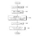
次に、上述の実施形態にかかる露光装置を用いたデバイス製造方法について説明する。図9は、半導体デバイスの製造工程を示すフローチャートである。図9に示すように、半導体デバイスの製造工程では、半導体デバイスの基板となるウェハに金属膜を蒸着し(ステップS40)、この蒸着した金属膜上に感光性材料であるフォトレジストを塗布する(ステップS42)。つづいて、上述の実施形態の露光装置を用い、レチクル(マスク)に形成されたパターンをウェハ上の各ショット領域(露光領域)に転写し(ステップS44:露光工程)、この転写が終了したウェハの現像、つまりパターンが転写されたフォトレジストの現像を行う(ステップS46:現像工程)。その後、ステップS46によってウェハの表面に生成されたレジストパターンをウェハ加工用のマスクとし、ウェハの表面に対してエッチング等の加工を行う(ステップS48:加工工程)。 Next, a device manufacturing method using the exposure apparatus according to the above-described embodiment will be described. FIG. 9 is a flowchart showing a semiconductor device manufacturing process. As shown in FIG. 9, in the semiconductor device manufacturing process, a metal film is vapor-deposited on a wafer to be a semiconductor device substrate (step S40), and a photoresist, which is a photosensitive material, is applied on the vapor-deposited metal film ( Step S42). Subsequently, using the exposure apparatus of the above-described embodiment, the pattern formed on the reticle (mask) is transferred to each shot area (exposure area) on the wafer (step S44: exposure process), and this transfer is completed. Development, that is, development of the photoresist to which the pattern has been transferred (step S46: development process). Thereafter, the resist pattern generated on the surface of the wafer in step S46 is used as a mask for wafer processing, and processing such as etching is performed on the surface of the wafer (step S48: processing step).
ここで、レジストパターンとは、上述の実施形態の露光装置によって転写されたパターンに対応する形状の凹凸が生成されたフォトレジスト層(転写パターン層)であって、その凹部がフォトレジスト層を貫通しているものである。ステップS48では、このレジストパターンを介してウェハの表面の加工を行う。ステップS48で行われる加工には、例えばウェハの表面のエッチングまたは金属膜等の成膜の少なくとも一方が含まれる。なお、ステップS44では、上述の実施形態の露光装置は、フォトレジストが塗布されたウェハを感光性基板としてパターンの転写を行う。 Here, the resist pattern is a photoresist layer (transfer pattern layer) in which unevenness having a shape corresponding to the pattern transferred by the exposure apparatus of the above-described embodiment is generated, and the recess penetrates the photoresist layer. It is what you are doing. In step S48, the surface of the wafer is processed through this resist pattern. The processing performed in step S48 includes, for example, at least one of etching of the wafer surface or film formation of a metal film or the like. In step S44, the exposure apparatus according to the above-described embodiment performs pattern transfer using the photoresist-coated wafer as a photosensitive substrate.
図10は、液晶表示素子等の液晶デバイスの製造工程を示すフローチャートである。図10に示すように、液晶デバイスの製造工程では、パターン形成工程(ステップS50)、カラーフィルタ形成工程(ステップS52)、セル組立工程(ステップS54)およびモジュール組立工程(ステップS56)を順次行う。ステップS50のパターン形成工程では、感光性基板としてフォトレジストが塗布されたガラス基板上に、上述の実施形態の投影露光装置を用いて回路パターンおよび電極パターン等の所定のパターンを形成する。このパターン形成工程には、上述の実施形態の露光装置を用いてフォトレジスト層にパターンを転写する露光工程と、パターンが転写された感光性基板の現像、つまりガラス基板上のフォトレジスト層の現像を行い、パターンに対応する形状のフォトレジスト層(転写パターン層)を生成する現像工程と、この現像されたフォトレジスト層を介してガラス基板の表面を加工する加工工程とが含まれている。 FIG. 10 is a flowchart showing a manufacturing process of a liquid crystal device such as a liquid crystal display element. As shown in FIG. 10, in the manufacturing process of the liquid crystal device, a pattern formation process (step S50), a color filter formation process (step S52), a cell assembly process (step S54), and a module assembly process (step S56) are sequentially performed. In the pattern forming step of step S50, predetermined patterns such as a circuit pattern and an electrode pattern are formed on the glass substrate coated with a photoresist as the photosensitive substrate, using the projection exposure apparatus of the above-described embodiment. The pattern forming process includes an exposure process in which a pattern is transferred to a photoresist layer using the exposure apparatus of the above-described embodiment, and development of a photosensitive substrate to which the pattern is transferred, that is, development of a photoresist layer on a glass substrate. And a development step for generating a photoresist layer (transfer pattern layer) having a shape corresponding to the pattern, and a processing step for processing the surface of the glass substrate through the developed photoresist layer.
ステップS52のカラーフィルタ形成工程では、R(Red)、G(Green)、B(Blue)に対応する3つのドットの組をマトリックス状に多数配列するか、またはR、G、Bの3本のストライプのフィルタの組を水平走査方向に複数配列したカラーフィルタを形成する。ステップS54のセル組立工程では、ステップS50によって所定パターンが形成されたガラス基板と、ステップS52によって形成されたカラーフィルタとを用いて液晶パネル(液晶セル)を組み立てる。具体的には、例えばガラス基板とカラーフィルタとの間に液晶を注入することで液晶パネルを形成する。ステップS56のモジュール組立工程では、ステップS54によって組み立てられた液晶パネルに対し、この液晶パネルの表示動作を行わせる電気回路およびバックライト等の各種部品を取り付ける。 In the color filter forming process in step S52, a large number of sets of three dots corresponding to R (Red), G (Green), and B (Blue) are arranged in a matrix or three R, G, and B A color filter is formed by arranging a plurality of stripe filter sets in the horizontal scanning direction. In the cell assembly process in step S54, a liquid crystal panel (liquid crystal cell) is assembled using the glass substrate on which the predetermined pattern is formed in step S50 and the color filter formed in step S52. Specifically, for example, a liquid crystal panel is formed by injecting liquid crystal between a glass substrate and a color filter. In the module assembling process in step S56, various components such as an electric circuit and a backlight for performing the display operation of the liquid crystal panel are attached to the liquid crystal panel assembled in step S54.
なお、本発明は、半導体デバイスまたは液晶デバイス製造用の露光装置への適用に限定されることなく、例えば、プラズマディスプレイ等のディスプレイ装置用の露光装置や、撮像素子(CCD等)、マイクロマシーン、薄膜磁気ヘッド、及びDNAチップ等の各種デバイスを製造するための露光装置にも広く適用できる。更に、本発明は、各種デバイスのマスクパターンが形成されたマスク(フォトマスク、レチクル等)をフォトリソグラフィ工程を用いて製造する際の、露光工程(露光装置)にも適用することができる。 The present invention is not limited to application to an exposure apparatus for manufacturing a semiconductor device or a liquid crystal device. For example, an exposure apparatus for a display device such as a plasma display, an image sensor (CCD or the like), a micromachine, The present invention can be widely applied to an exposure apparatus for manufacturing various devices such as a thin film magnetic head and a DNA chip. Furthermore, the present invention can also be applied to an exposure process (exposure apparatus) when manufacturing a mask (photomask, reticle, etc.) on which mask patterns of various devices are formed using a photolithography process.
また、上述の実施形態では、マルチ走査型の露光装置に搭載されてマスクのパターンの拡大像を形成する投影光学系に対して本発明を適用した例を示している。しかしながら、これに限定されることなく、一般に第1面の第1領域の像(拡大像、縮小像または等倍像)を第2面の第2領域に形成する反射屈折型の投影光学系に対しても同様に、本発明を適用することができる。また、1つの投影光学系を介して第1面に配置されるパターンを第2面に配置される基板へ走査露光または一括露光する露光装置などに対しても同様に、本発明を適用することができる。 In the above-described embodiment, an example is shown in which the present invention is applied to a projection optical system that is mounted on a multi-scanning exposure apparatus and forms an enlarged image of a mask pattern. However, the present invention is not limited to this, and in general, a catadioptric projection optical system that forms an image (enlarged image, reduced image, or equal-magnification image) of the first region of the first surface in the second region of the second surface Similarly, the present invention can be applied. Similarly, the present invention is also applied to an exposure apparatus that performs scanning exposure or batch exposure of a pattern arranged on the first surface to a substrate arranged on the second surface via one projection optical system. Can do.
MA マスク
IF 照明領域
PT プレート
EF 露光領域
PL 投影光学系
G1 第1レンズ群
G2 第2レンズ群
G3 第3レンズ群
CMa 曲面状の反射面
FMa 平面状の反射面
MA mask IF illumination area PT plate EF exposure area PL projection optical system G1 first lens group G2 second lens group G3 third lens group CMa Curved reflecting surface FMa Planar reflecting surface
Claims (19)
正の屈折力を有する第1レンズ群と、
前記第1レンズ群を介した前記第1領域からの光を前記第1面側に反射する曲面状の反射面と、
前記曲面状の反射面が反射した光を前記第2面側に反射する平面状の反射面と、
正の屈折力を有し、前記平面状の反射面が反射した光を前記第2領域に集光する第2レンズ群とを備え、
前記第1レンズ群、前記第2レンズ群及び前記曲面状の反射面は、直線状の1本の光軸に沿って共軸に配置され、
前記平面状の反射面は、前記1本の光軸に対して偏心配置されていることを特徴とする投影光学系。 In a catadioptric projection optical system that forms an image of a first region of a first surface in a second region of a second surface,
A first lens group having a positive refractive power;
A curved reflecting surface that reflects light from the first region via the first lens group toward the first surface;
A planar reflecting surface that reflects the light reflected by the curved reflecting surface toward the second surface;
A second lens group having a positive refractive power and condensing the light reflected by the planar reflecting surface on the second region;
The first lens group, the second lens group, and the curved reflecting surface are arranged coaxially along one linear optical axis,
The projection optical system, wherein the planar reflecting surface is arranged eccentrically with respect to the one optical axis.
0.7<dm/f<1
の条件を満足することを特徴とする請求項1乃至4のいずれか1項に記載の投影光学系。 When the focal length of the first lens group is f, the said one of the distance along the optical axis between the curved reflecting surface and the planar reflection surface and d m,
0.7 <d m / f <1
The projection optical system according to claim 1, wherein the following condition is satisfied.
0.9<dm/f<1
の条件を満足することを特徴とする請求項1乃至4のいずれか1項に記載の投影光学系。 When the focal length of the first lens group is f, the said one of the distance along the optical axis between the curved reflecting surface and the planar reflection surface and d m,
0.9 <d m / f <1
The projection optical system according to claim 1, wherein the following condition is satisfied.
0.5<(|f1|/f2)/(f/(f−f2))<1
の条件を満足することを特徴とする請求項7に記載の投影光学系。 When the focal length of the first lens group is f, the focal length of the negative lens group is f1, and the focal length of the positive lens group is f2,
0.5 <(| f1 | / f2) / (f / (f−f2)) <1
The projection optical system according to claim 7, wherein the following condition is satisfied.
請求項1乃至15のいずれか1項に記載の投影光学系を備え、
前記マスクステージは、前記パターンを前記第1面に配置し、
前記基板ステージは、前記感光性基板を前記第2面に配置することを特徴とする露光装置。 In an exposure apparatus that transfers an image of a mask pattern placed on a mask stage to a photosensitive substrate placed on a substrate stage,
A projection optical system according to any one of claims 1 to 15, comprising:
The mask stage arranges the pattern on the first surface,
The exposure apparatus characterized in that the substrate stage arranges the photosensitive substrate on the second surface.
前記パターンが転写された前記感光性基板を現像し、前記パターンに対応する形状の転写パターン層を前記感光性基板に形成する現像工程と、
前記転写パターン層を介して前記感光性基板を加工する加工工程とを含むことを特徴とするデバイス製造方法。 An exposure step of transferring the pattern to the photosensitive substrate using the exposure apparatus according to any one of claims 16 to 18,
Developing the photosensitive substrate to which the pattern has been transferred, and forming a transfer pattern layer having a shape corresponding to the pattern on the photosensitive substrate;
And a processing step of processing the photosensitive substrate through the transfer pattern layer.
Priority Applications (1)
| Application Number | Priority Date | Filing Date | Title |
|---|---|---|---|
| JP2008172004A JP5360529B2 (en) | 2008-07-01 | 2008-07-01 | Projection optical system, exposure apparatus, and device manufacturing method |
Applications Claiming Priority (1)
| Application Number | Priority Date | Filing Date | Title |
|---|---|---|---|
| JP2008172004A JP5360529B2 (en) | 2008-07-01 | 2008-07-01 | Projection optical system, exposure apparatus, and device manufacturing method |
Publications (2)
| Publication Number | Publication Date |
|---|---|
| JP2010014765A true JP2010014765A (en) | 2010-01-21 |
| JP5360529B2 JP5360529B2 (en) | 2013-12-04 |
Family
ID=41700962
Family Applications (1)
| Application Number | Title | Priority Date | Filing Date |
|---|---|---|---|
| JP2008172004A Active JP5360529B2 (en) | 2008-07-01 | 2008-07-01 | Projection optical system, exposure apparatus, and device manufacturing method |
Country Status (1)
| Country | Link |
|---|---|
| JP (1) | JP5360529B2 (en) |
Cited By (2)
| Publication number | Priority date | Publication date | Assignee | Title |
|---|---|---|---|---|
| WO2019064502A1 (en) * | 2017-09-29 | 2019-04-04 | 株式会社ニコン | Electron beam device and device manufacturing method |
| WO2019064503A1 (en) * | 2017-09-29 | 2019-04-04 | 株式会社ニコン | Electron beam device, illumination optical system, and method for manufacturing device |
Citations (5)
| Publication number | Priority date | Publication date | Assignee | Title |
|---|---|---|---|---|
| JP2001027727A (en) * | 1999-07-13 | 2001-01-30 | Nikon Corp | Reflective and refractive optical system and projection exposure device equipped with that optical system |
| JP2001228401A (en) * | 2000-02-16 | 2001-08-24 | Canon Inc | Projection optical system, projection aligner by this projection optical system and method for manufacturing device |
| JP2001343589A (en) * | 2000-03-31 | 2001-12-14 | Canon Inc | Projection optical system, projection exposure device by the same, manufacturing method of devices |
| JP2004271552A (en) * | 2003-03-05 | 2004-09-30 | Canon Inc | Enlarging and projecting optical system |
| JP2007286580A (en) * | 2006-03-20 | 2007-11-01 | Nikon Corp | Scanning type exposure apparatus, method of manufacturing micro-device, mask, projection optical apparatus, and method of manufacturing mask |
-
2008
- 2008-07-01 JP JP2008172004A patent/JP5360529B2/en active Active
Patent Citations (5)
| Publication number | Priority date | Publication date | Assignee | Title |
|---|---|---|---|---|
| JP2001027727A (en) * | 1999-07-13 | 2001-01-30 | Nikon Corp | Reflective and refractive optical system and projection exposure device equipped with that optical system |
| JP2001228401A (en) * | 2000-02-16 | 2001-08-24 | Canon Inc | Projection optical system, projection aligner by this projection optical system and method for manufacturing device |
| JP2001343589A (en) * | 2000-03-31 | 2001-12-14 | Canon Inc | Projection optical system, projection exposure device by the same, manufacturing method of devices |
| JP2004271552A (en) * | 2003-03-05 | 2004-09-30 | Canon Inc | Enlarging and projecting optical system |
| JP2007286580A (en) * | 2006-03-20 | 2007-11-01 | Nikon Corp | Scanning type exposure apparatus, method of manufacturing micro-device, mask, projection optical apparatus, and method of manufacturing mask |
Cited By (2)
| Publication number | Priority date | Publication date | Assignee | Title |
|---|---|---|---|---|
| WO2019064502A1 (en) * | 2017-09-29 | 2019-04-04 | 株式会社ニコン | Electron beam device and device manufacturing method |
| WO2019064503A1 (en) * | 2017-09-29 | 2019-04-04 | 株式会社ニコン | Electron beam device, illumination optical system, and method for manufacturing device |
Also Published As
| Publication number | Publication date |
|---|---|
| JP5360529B2 (en) | 2013-12-04 |
Similar Documents
| Publication | Publication Date | Title |
|---|---|---|
| US8102508B2 (en) | Projection optical system, exposure apparatus, and exposure method | |
| JP5360351B2 (en) | Projection optical system, exposure apparatus, and device manufacturing method | |
| JP5071382B2 (en) | Scanning exposure apparatus and microdevice manufacturing method | |
| EP1816502B1 (en) | Projection optical system, exposure equipment and exposure method | |
| EP1980890A1 (en) | Cata-dioptric imaging system, exposure device, and device manufacturing method | |
| US20090161087A1 (en) | Projection optical system, aligner, and method for fabricating device | |
| US6947121B2 (en) | Projection optical system, a projection exposure apparatus provided with the same, as well as a device manufacturing method | |
| JP2005340605A (en) | Aligner and its adjusting method | |
| JP2004145269A (en) | Projection optical system, reflective and refractive projection optical system, scanning exposure apparatus and exposure method | |
| JP2005003982A (en) | Projection optical system, and device and method of exposure | |
| KR100992302B1 (en) | Optical system, exposure apparatus and device manufacturing method | |
| JP5360529B2 (en) | Projection optical system, exposure apparatus, and device manufacturing method | |
| JP5110076B2 (en) | Catadioptric projection optical system, projection optical apparatus, and scanning exposure apparatus | |
| JP4868209B2 (en) | Projection optical system, exposure apparatus, and exposure method | |
| JP4547714B2 (en) | Projection optical system, exposure apparatus, and exposure method | |
| JP2007132981A (en) | Objective optical system, aberration measuring instrument and exposure device | |
| JP2005195713A (en) | Projection optical system, exposure device, and exposure method | |
| JP2000187332A (en) | Scanning projection aligner and exposing method | |
| JP5786919B2 (en) | Projection optical system, exposure apparatus and exposure method | |
| KR20010098613A (en) | Exposure apparatus and exposure method | |
| JP4729899B2 (en) | Scanning projection exposure apparatus, mask stage running correction method, and microdevice manufacturing method | |
| JP2004354555A (en) | Reflection refraction type projection optical system, exposing device and exposing method | |
| JP2004086110A (en) | Projection optical system, aligner, and exposure method | |
| JP2010002524A (en) | Projection optical system, exposure device, exposure method, and device manufacturing method | |
| JP2016136273A (en) | Projection optical system, exposure device, exposure method and device fabrication method |
Legal Events
| Date | Code | Title | Description |
|---|---|---|---|
| A621 | Written request for application examination |
Free format text: JAPANESE INTERMEDIATE CODE: A621 Effective date: 20110630 |
|
| A521 | Request for written amendment filed |
Free format text: JAPANESE INTERMEDIATE CODE: A523 Effective date: 20111207 |
|
| A977 | Report on retrieval |
Free format text: JAPANESE INTERMEDIATE CODE: A971007 Effective date: 20121219 |
|
| A131 | Notification of reasons for refusal |
Free format text: JAPANESE INTERMEDIATE CODE: A131 Effective date: 20121225 |
|
| A521 | Request for written amendment filed |
Free format text: JAPANESE INTERMEDIATE CODE: A523 Effective date: 20130212 |
|
| TRDD | Decision of grant or rejection written | ||
| A01 | Written decision to grant a patent or to grant a registration (utility model) |
Free format text: JAPANESE INTERMEDIATE CODE: A01 Effective date: 20130809 |
|
| A61 | First payment of annual fees (during grant procedure) |
Free format text: JAPANESE INTERMEDIATE CODE: A61 Effective date: 20130822 |
|
| R150 | Certificate of patent or registration of utility model |
Ref document number: 5360529 Country of ref document: JP Free format text: JAPANESE INTERMEDIATE CODE: R150 Free format text: JAPANESE INTERMEDIATE CODE: R150 |
|
| R250 | Receipt of annual fees |
Free format text: JAPANESE INTERMEDIATE CODE: R250 |
|
| R250 | Receipt of annual fees |
Free format text: JAPANESE INTERMEDIATE CODE: R250 |
|
| R250 | Receipt of annual fees |
Free format text: JAPANESE INTERMEDIATE CODE: R250 |
|
| R250 | Receipt of annual fees |
Free format text: JAPANESE INTERMEDIATE CODE: R250 |
|
| R250 | Receipt of annual fees |
Free format text: JAPANESE INTERMEDIATE CODE: R250 |
|
| R250 | Receipt of annual fees |
Free format text: JAPANESE INTERMEDIATE CODE: R250 |
|
| R250 | Receipt of annual fees |
Free format text: JAPANESE INTERMEDIATE CODE: R250 |
|
| R250 | Receipt of annual fees |
Free format text: JAPANESE INTERMEDIATE CODE: R250 |