JP5090451B2 - Method for forming carbon-containing silicon epitaxial layer - Google Patents
Method for forming carbon-containing silicon epitaxial layer Download PDFInfo
- Publication number
- JP5090451B2 JP5090451B2 JP2009522864A JP2009522864A JP5090451B2 JP 5090451 B2 JP5090451 B2 JP 5090451B2 JP 2009522864 A JP2009522864 A JP 2009522864A JP 2009522864 A JP2009522864 A JP 2009522864A JP 5090451 B2 JP5090451 B2 JP 5090451B2
- Authority
- JP
- Japan
- Prior art keywords
- epitaxial layer
- carbon
- silicon
- layer
- epitaxial
- Prior art date
- Legal status (The legal status is an assumption and is not a legal conclusion. Google has not performed a legal analysis and makes no representation as to the accuracy of the status listed.)
- Expired - Fee Related
Links
Images


Classifications
-
- C—CHEMISTRY; METALLURGY
- C30—CRYSTAL GROWTH
- C30B—SINGLE-CRYSTAL GROWTH; UNIDIRECTIONAL SOLIDIFICATION OF EUTECTIC MATERIAL OR UNIDIRECTIONAL DEMIXING OF EUTECTOID MATERIAL; REFINING BY ZONE-MELTING OF MATERIAL; PRODUCTION OF A HOMOGENEOUS POLYCRYSTALLINE MATERIAL WITH DEFINED STRUCTURE; SINGLE CRYSTALS OR HOMOGENEOUS POLYCRYSTALLINE MATERIAL WITH DEFINED STRUCTURE; AFTER-TREATMENT OF SINGLE CRYSTALS OR A HOMOGENEOUS POLYCRYSTALLINE MATERIAL WITH DEFINED STRUCTURE; APPARATUS THEREFOR
- C30B25/00—Single-crystal growth by chemical reaction of reactive gases, e.g. chemical vapour-deposition growth
- C30B25/02—Epitaxial-layer growth
-
- H—ELECTRICITY
- H01—ELECTRIC ELEMENTS
- H01L—SEMICONDUCTOR DEVICES NOT COVERED BY CLASS H10
- H01L21/00—Processes or apparatus adapted for the manufacture or treatment of semiconductor or solid state devices or of parts thereof
- H01L21/02—Manufacture or treatment of semiconductor devices or of parts thereof
- H01L21/04—Manufacture or treatment of semiconductor devices or of parts thereof the devices having at least one potential-jump barrier or surface barrier, e.g. PN junction, depletion layer or carrier concentration layer
- H01L21/18—Manufacture or treatment of semiconductor devices or of parts thereof the devices having at least one potential-jump barrier or surface barrier, e.g. PN junction, depletion layer or carrier concentration layer the devices having semiconductor bodies comprising elements of Group IV of the Periodic System or AIIIBV compounds with or without impurities, e.g. doping materials
- H01L21/20—Deposition of semiconductor materials on a substrate, e.g. epitaxial growth solid phase epitaxy
-
- C—CHEMISTRY; METALLURGY
- C30—CRYSTAL GROWTH
- C30B—SINGLE-CRYSTAL GROWTH; UNIDIRECTIONAL SOLIDIFICATION OF EUTECTIC MATERIAL OR UNIDIRECTIONAL DEMIXING OF EUTECTOID MATERIAL; REFINING BY ZONE-MELTING OF MATERIAL; PRODUCTION OF A HOMOGENEOUS POLYCRYSTALLINE MATERIAL WITH DEFINED STRUCTURE; SINGLE CRYSTALS OR HOMOGENEOUS POLYCRYSTALLINE MATERIAL WITH DEFINED STRUCTURE; AFTER-TREATMENT OF SINGLE CRYSTALS OR A HOMOGENEOUS POLYCRYSTALLINE MATERIAL WITH DEFINED STRUCTURE; APPARATUS THEREFOR
- C30B29/00—Single crystals or homogeneous polycrystalline material with defined structure characterised by the material or by their shape
- C30B29/02—Elements
- C30B29/06—Silicon
-
- H—ELECTRICITY
- H01—ELECTRIC ELEMENTS
- H01L—SEMICONDUCTOR DEVICES NOT COVERED BY CLASS H10
- H01L21/00—Processes or apparatus adapted for the manufacture or treatment of semiconductor or solid state devices or of parts thereof
- H01L21/02—Manufacture or treatment of semiconductor devices or of parts thereof
- H01L21/04—Manufacture or treatment of semiconductor devices or of parts thereof the devices having at least one potential-jump barrier or surface barrier, e.g. PN junction, depletion layer or carrier concentration layer
- H01L21/34—Manufacture or treatment of semiconductor devices or of parts thereof the devices having at least one potential-jump barrier or surface barrier, e.g. PN junction, depletion layer or carrier concentration layer the devices having semiconductor bodies not provided for in groups H01L21/0405, H01L21/0445, H01L21/06, H01L21/16 and H01L21/18 with or without impurities, e.g. doping materials
- H01L21/46—Treatment of semiconductor bodies using processes or apparatus not provided for in groups H01L21/428
- H01L21/461—Treatment of semiconductor bodies using processes or apparatus not provided for in groups H01L21/428 to change their surface-physical characteristics or shape, e.g. etching, polishing, cutting
- H01L21/4763—Deposition of non-insulating, e.g. conductive -, resistive -, layers on insulating layers; After-treatment of these layers
-
- H—ELECTRICITY
- H01—ELECTRIC ELEMENTS
- H01L—SEMICONDUCTOR DEVICES NOT COVERED BY CLASS H10
- H01L21/00—Processes or apparatus adapted for the manufacture or treatment of semiconductor or solid state devices or of parts thereof
- H01L21/70—Manufacture or treatment of devices consisting of a plurality of solid state components formed in or on a common substrate or of parts thereof; Manufacture of integrated circuit devices or of parts thereof
- H01L21/77—Manufacture or treatment of devices consisting of a plurality of solid state components or integrated circuits formed in, or on, a common substrate
- H01L21/78—Manufacture or treatment of devices consisting of a plurality of solid state components or integrated circuits formed in, or on, a common substrate with subsequent division of the substrate into plural individual devices
- H01L21/82—Manufacture or treatment of devices consisting of a plurality of solid state components or integrated circuits formed in, or on, a common substrate with subsequent division of the substrate into plural individual devices to produce devices, e.g. integrated circuits, each consisting of a plurality of components
- H01L21/822—Manufacture or treatment of devices consisting of a plurality of solid state components or integrated circuits formed in, or on, a common substrate with subsequent division of the substrate into plural individual devices to produce devices, e.g. integrated circuits, each consisting of a plurality of components the substrate being a semiconductor, using silicon technology
- H01L21/8232—Field-effect technology
- H01L21/8234—MIS technology, i.e. integration processes of field effect transistors of the conductor-insulator-semiconductor type
Description
本願は、2006年7月31日に出願された、発明の名称が“METHODOF FORMINGCARBON-CONTAINING SILICONEPITAXIAL LAYERS”(代理人整理番号1-0595/L)とされた、米国仮特許出願第60/834,773号の優先権を主張し、この開示内容は本明細書に全体で援用されている。 The present application is filed on July 31, 2006, and the name of the invention is “METHODF FORMING CARBON-CONTAINING SILICONEPITIAL LAYERS” (Attorney Docket No. 1-0595 / L), US Provisional Patent Application No. 60/834, No. 773 is claimed and this disclosure is incorporated herein in its entirety.
本願は、以下の同時係属出願に関連し、これらの開示内容の各々は、本明細書に全体で援用されている。 This application is related to the following copending applications, each of which is incorporated herein by reference in its entirety.
2004年12月1日に出願された米国特許出願第11/001,774号(整理番号9618)
2005年9月14日に出願された米国特許出願第11/227,974号(整理番号9618/P01)
US patent application Ser. No. 11 / 001,774 filed Dec. 1, 2004 (Docket No. 9618)
U.S. Patent Application No. 11 / 227,974, filed September 14, 2005 (Docket No. 9618 / P01)
本発明は、半導体デバイスの製造、より詳細には、炭素含有シリコンエピタキシャル層の形成方法に関する。
背景
より小さいトランジスタが製造されるにつれて、極浅ソース/ドレイン接合を作るのがより難しくなってきている。一般的に、100nm以下の(sub-100nm)CMOS(相補型金属酸化物半導体)デバイスは、30nm未満の接合深さを必要とする。シリコン含有材料(例えば、Si、SiGe、SiC)のエピ層を接合中に形成するのに、選択的エピタキシャル堆積がしばしば利用される。一般的に、選択的エピタキシャル堆積は、エピ層を誘電領域に成長させることなく、シリコンモート(moats)上に成長させることができる。選択的エピタキシーは、隆起したソース/ドレイン、ソース/ドレイン拡大部、コンタクトプラグ又はバイポーラデバイスのベース層堆積のような半導体デバイス内で用いることができる。
The present invention relates to semiconductor device manufacturing, and more particularly to a method for forming a carbon-containing silicon epitaxial layer.
Background As smaller transistors are manufactured, it is becoming more difficult to make very shallow source / drain junctions. In general, sub-100 nm (sub-100 nm) CMOS (complementary metal oxide semiconductor) devices require a junction depth of less than 30 nm. Selective epitaxial deposition is often used to form epilayers of silicon-containing materials (eg, Si, SiGe, SiC) in the junction. In general, selective epitaxial deposition can be grown on silicon moats without growing an epi layer in the dielectric region. Selective epitaxy can be used in semiconductor devices such as raised source / drains, source / drain extensions, contact plugs or base layer deposition of bipolar devices.
一般的に、選択的エピタキシープロセスは、堆積反応とエッチング反応とを含む。堆積反応とエッチング反応は、エピタキシャル層に対するのと、多結晶層に対するのとで相対的に異なる反応速度で同時に生じる。堆積プロセス中、エピタキシャル層が単結晶層上に形成され、一方、多結晶層は、既存の多結晶層及び/又はアモルファス層のような、少なくとも第二層上に堆積される。しかしながら、堆積された多結晶層は、一般的にエピタキシャル層よりも速い速度でエッチングされる。それ故、エッチャントガスの濃度を変えることによって、正味の選択的プロセスは、エピタキシー材料の堆積と、限られた多結晶材料の堆積又は多結晶材料は堆積しない結果となる。例えば、選択的エピタキシープロセスは、スペーサ上に堆積を残さずに、単結晶シリコン表面上のシリコン含有材料のエピ層の形成を生じる場合がある。 In general, the selective epitaxy process includes a deposition reaction and an etching reaction. The deposition reaction and the etching reaction occur simultaneously at relatively different reaction rates for the epitaxial layer and for the polycrystalline layer. During the deposition process, an epitaxial layer is formed on the single crystal layer, while the polycrystalline layer is deposited on at least a second layer, such as an existing polycrystalline layer and / or an amorphous layer. However, the deposited polycrystalline layer is generally etched at a faster rate than the epitaxial layer. Therefore, by changing the etchant gas concentration, the net selective process results in deposition of epitaxy material and limited deposition of polycrystalline material or no polycrystalline material. For example, a selective epitaxy process may result in the formation of an epilayer of a silicon-containing material on a single crystal silicon surface without leaving a deposition on the spacer.
隆起したソース/ドレイン特徴部やソース/ドレイン拡大部の特徴部の形成中、例えば、シリコン含有MOSFET(金属酸化物半導体電界効果トランジスタ)デバイスの形成中、シリコン含有材料の選択的エピタキシー堆積は、有益な技術になってきている。ソース/ドレイン拡大部の特徴部は、シリコン表面をエッチングして、凹んだソース/ドレイン特徴部を作り、続いて、エッチングされた表面を、選択的成長エピ層(epilayer)、例えば、シリコンゲルマニウム(SiGe)材料で充填することによって製造する。選択的エピタキシーは、インサイチュドーピングで完全に近いドーパント活性化を可能にするので、その後のアニールプロセスが省略される。それ故、接合深さを、シリコンエッチングと選択的エピタキシーによって正確に画成することができる。他方で、超浅ソース/ドレイン接合は、直列抵抗の増加を必然的に生じる。 During the formation of raised source / drain features and source / drain extension features, for example, during the formation of silicon-containing MOSFET (metal oxide semiconductor field effect transistor) devices, selective epitaxy deposition of silicon-containing materials is beneficial. Has become a new technology. The source / drain extension feature etches the silicon surface to create a recessed source / drain feature, which is then etched into a selectively grown epilayer, eg, silicon germanium ( Manufactured by filling with SiGe) material. Selective epitaxy allows near-perfect dopant activation with in situ doping, so that subsequent annealing processes are omitted. Therefore, the junction depth can be accurately defined by silicon etching and selective epitaxy. On the other hand, ultra shallow source / drain junctions inevitably result in increased series resistance.
また、シリサイド形成中の接合消失により、直列抵抗が更に増加する。接合消失を補償するために、隆起したソース/ドレインを、接合上に選択的にエピタキシャル成長させる。典型的には、隆起したソース/ドレイン層は、ドープされていないシリコンである。 Further, the series resistance further increases due to the disappearance of the junction during the formation of the silicide. In order to compensate for junction loss, raised source / drains are selectively epitaxially grown on the junction. Typically, the raised source / drain layers are undoped silicon.
しかしながら、現在の選択的エピタキシープロセスは、いくつかの欠点を有する。現在のエピタキシープロセス中、選択性を維持するために、前駆物質の化学的濃度と、反応温度を堆積プロセス全体を通して調節、調整しなければならない。十分なシリコン前駆物質が与えられない場合には、エッチング反応が支配的になり、全体のプロセスが減速する。また、基板特徴部の有害なオーバーエッチングが起こることがある。十分なエッチャント前駆物質が与えられない場合には、堆積反応が支配的になり、基板表面にわたって単結晶及び多結晶材料を形成させる選択性を減少することがある。また、現在の選択的エピタキシープロセスは、通常、約800℃、1,000℃又はそれより高い反応温度を要求する。このような高温は、熱量上の理由と基板表面の制御できない窒化物形成反応の可能性により、製造プロセス中は望ましくない。更に、いくつかのエピタキシャル膜及び/又はプロセスは、膜中のピッチング或いは表面粗さのような形態的な欠陥を生じる傾向がある。 However, current selective epitaxy processes have several drawbacks. In order to maintain selectivity during current epitaxy processes, the chemical concentration of the precursors and the reaction temperature must be adjusted and adjusted throughout the deposition process. If not enough silicon precursor is provided, the etching reaction becomes dominant and the overall process is slowed down. Also, detrimental over-etching of substrate features can occur. If not enough etchant precursor is provided, the deposition reaction may dominate and reduce the selectivity to form single crystal and polycrystalline materials across the substrate surface. Also, current selective epitaxy processes typically require reaction temperatures of about 800 ° C., 1,000 ° C. or higher. Such high temperatures are undesirable during the manufacturing process due to the amount of heat and the possibility of uncontrollable nitridation reactions on the substrate surface. In addition, some epitaxial films and / or processes tend to produce morphological defects such as pitting or surface roughness in the film.
それ故、シリコンやシリコン含有化合物を選択的にエピタキシャル堆積するためのプロセスの必要がある。更に、このプロセスは、速い堆積速度を有し、約800℃以下のようなプロセス温度を維持しながら、様々な元素濃度を有するシリコン含有化合物を形成する用途にも用いることができなければならない。最後に、プロセスは、低欠陥膜或いは膜スタック(例えば、ピッチング、転位、粗さ、点欠陥等が殆どない)を生じることができなければならない。 Therefore, there is a need for a process for selectively epitaxially depositing silicon and silicon-containing compounds. In addition, this process should have a high deposition rate and be able to be used in applications that form silicon-containing compounds with varying elemental concentrations while maintaining process temperatures such as about 800 ° C. or less. Finally, the process must be able to produce low defect films or film stacks (eg, few pitching, dislocations, roughness, point defects, etc.).
本発明の第一態様では、基板上にエピタキシャル層スタックを形成する方法が提供される。本方法は、(1)エピタキシャル層スタックのためのターゲット炭素濃度を選択するステップと、(2)基板上に炭素含有シリコン層を形成するステップであって、炭素含有シリコン層が、選択されたターゲット炭素濃度に基づいて選択される初期炭素濃度、厚さ及び堆積時間の少なくとも一つを有する、前記ステップと、(3)エッチングの前に、炭素含有シリコン層上に炭素を含有しないシリコン層を形成するステップと、を含む。 In a first aspect of the invention, a method is provided for forming an epitaxial layer stack on a substrate. The method includes (1) selecting a target carbon concentration for the epitaxial layer stack, and (2) forming a carbon-containing silicon layer on the substrate, wherein the carbon-containing silicon layer is the selected target. Said step having at least one of an initial carbon concentration, thickness and deposition time selected based on the carbon concentration, and (3) forming a carbon-free silicon layer on the carbon-containing silicon layer prior to etching Including the steps of:
本発明の第二態様では、エピタキシャル層スタックを形成する方法が提供される。この方法は、(1)エピタキシャル層スタックのためのターゲット炭素濃度を選択するステップと、(2)交互の炭素含有シリコン層と炭素を含有しないシリコン層を堆積させることによって、エピタキシャル層スタックを形成するステップとを含む。ターゲット炭素濃度は、全体の厚さ、初期炭素濃度、及び炭素含有シリコン層の堆積時間の少なくとも1つに基づいて達成される。 In a second aspect of the present invention, a method for forming an epitaxial layer stack is provided. The method forms an epitaxial layer stack by (1) selecting a target carbon concentration for the epitaxial layer stack and (2) depositing alternating carbon-containing silicon layers and carbon-free silicon layers. Steps. The target carbon concentration is achieved based on at least one of the overall thickness, the initial carbon concentration, and the deposition time of the carbon-containing silicon layer.
本発明の第三態様では、基板上に形成されたエピタキシャル層スタックの炭素濃度を制御するための方法が提供される。この方法は、(1)エピタキシャル層スタックの望ましい炭素濃度を決定するステップと、(2)(a)基板上に炭素含有エピタキシャル層を形成し、(b)炭素含有エピタキシャル層上に炭素を含有しないエピタキシャル層を形成することによって、エピタキシャル層スタックを形成するステップと、を含む。炭素含有エピタキシャル層の厚さは、エピタキシャル層スタックの望ましい炭素濃度に基づいて選択される。多数の他の態様も提供される。 In a third aspect of the invention, a method is provided for controlling the carbon concentration of an epitaxial layer stack formed on a substrate. The method includes (1) determining a desired carbon concentration of the epitaxial layer stack; (2) (a) forming a carbon-containing epitaxial layer on the substrate; and (b) not containing carbon on the carbon-containing epitaxial layer. Forming an epitaxial layer stack by forming an epitaxial layer. The thickness of the carbon-containing epitaxial layer is selected based on the desired carbon concentration of the epitaxial layer stack. Numerous other aspects are also provided.
本発明の他の特徴及び態様は以下の詳細な説明、添付した特許請求の範囲、添付図面からより十分に明らかになるであろう。 Other features and aspects of the present invention will become more fully apparent from the following detailed description, the appended claims and the accompanying drawings.
誘電膜でパターン形成されたシリコン基板上の選択的エピタキシャル成長プロセス中、単結晶半導体の形成は、露出したシリコン表面上(例えば、誘電表面上ではなく)でのみ生じる。選択的エピタキシャル成長プロセスは、同時に起こるエッチング堆積プロセスと、交互のガス供給プロセスを含むことがある。同時に起こるエッチング堆積プロセスでは、エッチャント化学種と堆積化学種の両方が、同時に流される。このようにして、エピタキシャル層は、その形成中、同時に堆積され且つエッチングされる。 During a selective epitaxial growth process on a silicon substrate patterned with a dielectric film, the formation of a single crystal semiconductor occurs only on the exposed silicon surface (eg, not on the dielectric surface). The selective epitaxial growth process may include simultaneous etch deposition processes and alternating gas supply processes. In a simultaneous etch deposition process, both etchant species and deposition species are flowed simultaneously. In this way, the epitaxial layer is deposited and etched simultaneously during its formation.
一方、先に援用した、2004年12月1日に出願された米国特許出願第11/001,774号(整理番号9618)は、基板上にエピタキシャル層を形成するための交互のガス供給(AGS)プロセスを記載する。AGSプロセス中、エピタキシャル堆積プロセスが基板上で行われ、次いで、エッチングプロセスが基板上で行われる。エピタキシャル層の望ましい厚さが形成されるまで、エピタキシャル堆積プロセスの後にエッチングプロセスが続くサイクルが繰り返される。 On the other hand, previously incorporated US patent application Ser. No. 11 / 001,774 filed Dec. 1, 2004 (Docket No. 9618) is an alternate gas supply (AGS) for forming an epitaxial layer on a substrate. ) Describe the process. During the AGS process, an epitaxial deposition process is performed on the substrate and then an etching process is performed on the substrate. The cycle of the epitaxial deposition process followed by the etching process is repeated until the desired thickness of the epitaxial layer is formed.
堆積プロセスは、基板表面を少なくともシリコン源とキャリアガスを含有する堆積ガスに曝すステップを含んでもよい。堆積ガスは、また、ゲルマニウム及び/又は炭素源だけでなく、ドーパント源を含んでもよい。一般的なドーパントとしては、ヒ素、ホウ素、リン、アンチモン、ガリウム、アルミニウム、他の元素を挙げることができる。 The deposition process may include exposing the substrate surface to a deposition gas containing at least a silicon source and a carrier gas. The deposition gas may also include a dopant source as well as a germanium and / or carbon source. Common dopants include arsenic, boron, phosphorus, antimony, gallium, aluminum, and other elements.
堆積プロセス中、エピタキシャル層は、一つ又は複数の基板の単結晶表面上に形成され、一方、多結晶層が、アモルファス及び/又は多結晶表面のような二次表面上に形成される。続いて、基板がエッチングガスに曝される。エッチングガスは、キャリアガスとエッチャントとを含む。エッチングガスは、堆積中に堆積されたシリコン含有材料を除去する。エッチングプロセス中、多結晶層が、エピタキシャル層よりも速い速度で除去される。それ故、堆積とエッチングプロセスの最終結果は、単結晶表面上のシリコン含有材料のエピタキシャル成長を形成し、もしあったとしても、二次表面上の多結晶シリコン含有材料の成長は最小限である。堆積することができる例示的なシリコン含有材料としては、シリコン、シリコンゲルマニウム、シリコン炭素、シリコンゲルマニウム炭素、これらのドーパント変形例等が挙げれる。 During the deposition process, an epitaxial layer is formed on a single crystal surface of one or more substrates, while a polycrystalline layer is formed on a secondary surface, such as an amorphous and / or polycrystalline surface. Subsequently, the substrate is exposed to an etching gas. The etching gas includes a carrier gas and an etchant. The etching gas removes the silicon-containing material deposited during deposition. During the etching process, the polycrystalline layer is removed at a faster rate than the epitaxial layer. Therefore, the end result of the deposition and etching process forms an epitaxial growth of the silicon-containing material on the single crystal surface, and the growth of the polycrystalline silicon-containing material on the secondary surface, if any, is minimal. Exemplary silicon-containing materials that can be deposited include silicon, silicon germanium, silicon carbon, silicon germanium carbon, dopant variations thereof, and the like.
従来のシリコンエピタキシャル膜形成プロセスは、水素(H2)、塩化水素(HCl)、ジクロロシランのようなシリコン源を用いて、(例えば、HCl及び/又はシリコン源を解離させるために)約700℃より高い基板温度で行われる。Cl2はより低い温度(例えば、約600℃以下)で効率的に解離するので、エピタキシャル膜形成温度を下げる一つの方法は、HClの代わりに塩素(Cl2)を用いることである。水素とCl2は非相溶性であることから、水素以外の、例えば、窒素のようなキャリアガスをCl2と用いるのがよい。同様に、より低い解離温度を有するシリコン源を用いるのがよい(例えば、シラン(SiH4)、ジシラン(Si2H6)等)。 A conventional silicon epitaxial film formation process uses a silicon source such as hydrogen (H 2 ), hydrogen chloride (HCl), dichlorosilane, for example, at about 700 ° C. (to dissociate HCl and / or the silicon source). Performed at a higher substrate temperature. Since Cl 2 dissociates efficiently at lower temperatures (eg, about 600 ° C. or less), one way to lower the epitaxial film formation temperature is to use chlorine (Cl 2 ) instead of HCl. Since hydrogen and Cl 2 are incompatible, it is preferable to use a carrier gas other than hydrogen, such as nitrogen, for example, with Cl 2 . Similarly, a silicon source having a lower dissociation temperature may be used (eg, silane (SiH 4 ), disilane (Si 2 H 6 ), etc.).
シリコンエピタキシャル膜形成プロセスのエッチャントガスとしてCl2を用いることにより、生じるシリコンエピタキシャル膜の表面形態が悪くなる場合がある。いかなる特定の理論に縛られることは望まないが、Cl2は、シリコンエピタキシャル膜表面を過度に激しく攻撃して、ピッチング等を生じるのであろうと考えられる。シリコンエピタキシャル膜が炭素を含有するときに、Cl2を用いると特に問題があることが分かってきた。 By using Cl 2 as an etchant gas in the silicon epitaxial film formation process, the surface morphology of the resulting silicon epitaxial film may be deteriorated. Although not wishing to be bound by any particular theory, it is believed that Cl 2 will attack the silicon epitaxial film surface too violently, resulting in pitching and the like. It has been found that there is a particular problem with using Cl 2 when the silicon epitaxial film contains carbon.
本発明は、エピタキシャル膜表面形態を改善することができるシリコンエピタキシャル膜形成プロセス中、エッチャントガスとしてCl2を用いる方法を提供する。本発明の方法は、例えば、2004年12月1日に出願された米国特許出願第11/001,774号(整理番号9618)に記載された交互のガス供給(AGS)プロセスとともに用いることもできる。 The present invention provides a method of using Cl 2 as an etchant gas during a silicon epitaxial film formation process that can improve the epitaxial film surface morphology. The method of the present invention can also be used in conjunction with the alternating gas supply (AGS) process described, for example, in US patent application Ser. No. 11 / 001,774 filed Dec. 1, 2004 (Docket No. 9618). .
ある実施形態では、エッチング段階中、Cl2に曝される前に、いかなる炭素含有シリコンエピタキシャル膜をも“封入”されるのがよい。炭素含有シリコンエピタキシャル膜は、例えば、炭素源なしに形成されたシリコンエピタキシャル膜(“炭素を含有しないシリコンエピタキシャル膜”)によって、封入することができる。 In certain embodiments, any carbon-containing silicon epitaxial film may be “encapsulated” prior to exposure to Cl 2 during the etching step. The carbon-containing silicon epitaxial film can be encapsulated by, for example, a silicon epitaxial film formed without a carbon source (“silicon epitaxial film not containing carbon”).
例示として、本発明による、AGSプロセスを用いた、炭素含有シリコンエピタキシャル層スタックの形成を図1A-図1Dを参照して以下に記載する。図1Aを参照すると、基板100上にエピタキシャルシード層102(例えば、シリコン(Si)エピタキシャル層)が形成された基板100の断面図を示す。ある実施形態では、エピタキシャルシード層102は、除かれる。
By way of example, the formation of a carbon-containing silicon epitaxial layer stack using the AGS process according to the present invention is described below with reference to FIGS. 1A-1D. Referring to FIG. 1A, a cross-sectional view of a
エピタキシャルシード層102を形成するために、基板100をプロセスチャンバ内に配置し、望ましい基板及び/又はプロセス温度まで加熱する。例示的なエピタキシャル膜チャンバは、カリフォルニア州サンタクララにあるAppliedMaterials社のEpi Centure(登録商標)システムやPoly Gen(登録商標)システムに見られるが、他のエピタキシャル膜チャンバ及び/又はシステムを用いることができる。本発明の少なくとも1つの実施形態では、プロセスチャンバ内でいかなるシリコンエピタキシャル層中にも炭素が混入することを改善するために、約700℃未満の基板及び/又はプロセス温度を用いるのがよい。特定の実施形態では、約550〜650℃の基板及び/又はプロセス温度範囲を用いるのがよく、更に他の実施形態では、約600℃未満の基板及び/又はプロセス温度を用いるのがよい。700℃より高い基板及び/又はプロセス温度を含む、他の基板及び/又はプロセス温度を用いてもよい。
To form the
望ましい基板及び/又はプロセス温度に達した後、基板100を、少なくともシリコン源(炭素源なしで)に曝して、エピタキシャルシード層102を形成する。例えば、基板100をシラン或いはジシランのようなシリコン源と、窒素のようなキャリアガスに曝すのがよい。リン或いはホウ素のようなドーパント源、ゲルマニウム源等も(いかなる他の適当なソース及び/又はガスであってもよいように)用いることができる。エピタキシャル膜形成プロセス中、基板100のいかなる単結晶表面上にもエピタキシャル層102が形成され、一方、(前述したように)基板100上に存在するいかなる多結晶層及び/又はいかなるアモルファス層上にも多結晶層が形成される。
After reaching the desired substrate and / or process temperature, the
エピタキシャルシード層102は、例えば、シランを約50-150sccmの流量で(或いはジシランを約10-40sccmの流量で)シリコン源を流し、約20-25slmの流量で窒素キャリアガスを流すことによって(より大きい或いは小さいシリコン源及び/又はキャリアガス流量を用いてもよいが)形成される。必要に応じてHClを流してもよい。
The
少なくとも一つの実施形態では、エピタキシャルシード層102は、約2オングストローム〜約10オングストロームの厚さを有するのがよいが、他の厚さが用いられてもよい。例えば、約1秒〜約100秒の堆積時間を、一つ以上の実施形態においては約5秒を、用いることができる。
In at least one embodiment, the
エピタキシャルシード層102(少しでも用いた場合には)を形成した後、基板100を少なくともシリコン源と炭素源に曝して、炭素含有シリコンエピタキシャル層104(図1B)を基板100上にエピタキシャルシード層102の上に形成する。例えば、基板100をシラン或いはジシランのようなシリコン源、メタンのような炭素源と、窒素のようなキャリアガスに曝すのがよい。リン或いはホウ素のようなドーパント源、ゲルマニウム源等も(いかなる他の適当なソース及び/又はガスでもよいように)用いることができる。エピタキシャル膜形成プロセス中、炭素含有エピタキシャル層が、基板100のいかなる単結晶表面上にも形成され、一方、(前述したように)基板100上に存在するいかなる多結晶層及び/又はいかなるアモルファス層上にも多結晶層が形成される。
After forming the epitaxial seed layer 102 (if used at all), the
少なくとも一つの実施形態では、メタンの約1-5sccmの炭素源流量を、シランの約50-150sccm(或いはジシランの約10-40sccm)のシリコン源流量と約20-25slmの流量の窒素キャリアガスとともに用いるのがよい(より大きい或いは小さいシリコン源及び/又はキャリアガス流量を用いてもよい)。必要に応じてHClを流してもよい。 In at least one embodiment, a carbon source flow rate of about 1-5 sccm of methane with a silicon source flow rate of about 50-150 sccm of silane (or about 10-40 sccm of disilane) and a nitrogen carrier gas at a flow rate of about 20-25 slm. It may be used (a larger or smaller silicon source and / or carrier gas flow rate may be used). HCl may be flowed as necessary.
炭素含有エピタキシャル層104は、例えば、約2オングストローム〜100オングストロームの厚さを有するのがよいが、他の厚さが用いられてもよい。例えば、約1秒〜約50秒の堆積時間を、一つ以上の実施形態においては約10秒を、用いることができる。
The carbon-containing
炭素含有シリコンエピタキシャル層104を形成した後、基板100を少なくともシリコン源に(炭素源なしに)曝して、第二シリコンエピタキシャル層106(例えば、図1Cに示すようなキャッピング層)を基板100上に炭素含有シリコンエピタキシャル層104の上に形成する。例えば、基板100をシラン或いはジシランのようなシリコン源と、窒素のようなキャリアガスに曝すのがよい。リン或いはホウ素のようなドーパント源、ゲルマニウム源等も(いかなる他の適当なソース及び/又はガスでもよいように)用いることができる。炭素含有シリコンエピタキシャル層104上に第二シリコンエピタキシャル層106が存在することにより、炭素含有シリコンエピタキシャル層104中の塩素と炭素(及び/又は水素)との相互作用を減らすことができる。前述したように、HClを流してもよい。
After forming the carbon-containing
第二シリコンエピタキシャル層106は、例えば、シランの約50-150sccmの流量(或いはジシランの約10-40sccmの流量)でシリコン源を流し、約20-25slmの流量で窒素キャリアガスを流すことによって(より大きい或いは小さいシリコン源及び/又はキャリアガス流量を用いてもよいが)、形成することができる。HClを流してもよい。
The second
少なくとも一つの実施形態では、第二シリコンエピタキシャル層106は、約2オングストローム〜100オングストロームの厚さを有するのがよいが、他の厚さが用いられてもよい。例えば、約1秒〜約100秒の堆積時間を、一つ以上の実施形態において約5秒を、用いることができる。
In at least one embodiment, the second
これによって、炭素含有エピタキシャル層104が、炭素を含有しないエピタキシャル層102、206(例えば、意図的な炭素源なしに形成されたエピタキシャル層)の間に封入された、エピタキシャル層スタック108が形成される。
This forms an
第二シリコンエピタキシャル層106の形成後、基板100をCl2及び/又は他のエッチャントに曝して、少なくとも第二シリコンエピタキシャル層106及び/又は基板100上に形成された他の膜(例えば、基板100上に存在する多結晶及び/又はアモルファス層上に形成された多結晶シリコン及び/又は炭素含有シリコンエピタキシャル層104上に形成された単結晶シリコン)をエッチングする。例えば、少なくとも一つの実施形態では、基板100を約30-50sccmの流量のCl2と20slmの流量の窒素キャリアガスに曝す。HClを流してもよい(より大きい或いは小さいCl2及び/又はキャリアガス流量を用いてもよい)。
After the formation of the second
エッチングの後、(例えば、窒素及び/又は他の不活性ガスで、約20秒或いは他の適当な時間中)使用されているプロセスチャンバがパージされ、いかなるCl2及び/又はいかなる他の望ましくない化学種/副生成物をチャンバから除去するのがよい。 After etching, the process chamber being used is purged (eg, with nitrogen and / or other inert gas for about 20 seconds or other suitable time), and any Cl 2 and / or any other undesirable Chemical species / by-products may be removed from the chamber.
エピタキシャルキャップ層106及び/又はシード層102は、エッチャントと炭素含有エピタキシャル層104の炭素との間で反応が生じるのを妨げる。このようなものとして、エッチング中、下にある炭素含有層はCl2に曝されないので、Cl2をエッチャントして用いるのがよい。従って、炭素含有エピタキシャル層102は、ピッチングを有する表面形態ではなく平滑な表面形態を有する。
例えば、図1Dに示されるように、望ましい全体のエピタキシャル層スタック厚さが達成されるまで、堆積とエッチングの順番を繰り返すのがよい。例えば、炭素を含有しないシリコン層堆積/炭素含有シリコン層堆積/炭素を含有しないシリコン層堆積/エッチングの順番を約80回繰り返して、約600オングストロームの全体のエピタキシャル層スタック厚さを生じるのがよい。他の実施形態では、下に横たわるシード層の堆積は除去されるので、形成の順番は、望ましい全体のエピタキシャル層スタック厚さを生じるために多数回繰り返される、炭素含有シリコン層堆積/炭素を含有しないシリコン層堆積/エッチングであるのがよい。 For example, as shown in FIG. 1D, the deposition and etch sequence may be repeated until the desired overall epitaxial layer stack thickness is achieved. For example, the sequence of carbon-free silicon layer deposition / carbon-containing silicon layer deposition / carbon-free silicon layer deposition / etching may be repeated about 80 times to produce a total epitaxial layer stack thickness of about 600 Å. . In other embodiments, the underlying seed layer deposition is removed so that the order of formation contains a carbon-containing silicon layer deposition / carbon that is repeated multiple times to produce the desired overall epitaxial layer stack thickness. Preferably no silicon layer deposition / etching.
上述の例示は、特定の実施形態を示すが、一般的には、エピタキシャル層スタック(炭素含有エピタキシャル層と炭素を含有しないエピタキシャル層を含む)は、約10オングストローム〜約2000オングストローム、好ましくは約100オングストローム〜約1500オングストローム、より好ましくは約300オングストローム〜約1000オングストロームの範囲の厚さを有する。一つの特定の実施形態では、約600オングストロームの層スタックを用いるのがよい。 The above illustration shows a specific embodiment, but in general, the epitaxial layer stack (including carbon-containing and carbon-free epitaxial layers) is about 10 angstroms to about 2000 angstroms, preferably about 100 angstroms. It has a thickness ranging from angstroms to about 1500 angstroms, more preferably from about 300 angstroms to about 1000 angstroms. In one particular embodiment, a layer stack of about 600 Angstroms may be used.
(1)炭素を含有しないエピタキシャル材料に対するカプセル被覆された炭素含有エピタキシャル層の膜厚と、(2)炭素含有エピタキシャル層の炭素濃度を制御することによって、最終的なエピタキシャル層スタックの平均炭素濃度を制御及び/又は決定することができる。例えば、ある実施形態では、炭素が炭素含有エピタキシャル層形成ステップ中に堆積されるのみであっても、一つ又は複数の炭素含有エピタキシャル層の炭素は、スタックされた層(例えば、シード層、炭素含有層、キャップ層)の深さに層って素早く且つ均一に拡散する。 (1) By controlling the film thickness of the encapsulated carbon-containing epitaxial layer relative to the carbon-free epitaxial material and (2) the carbon concentration of the carbon-containing epitaxial layer, the average carbon concentration of the final epitaxial layer stack is Can be controlled and / or determined. For example, in certain embodiments, the carbon of one or more carbon-containing epitaxial layers may be stacked layers (eg, seed layer, carbon, even if carbon is only deposited during the carbon-containing epitaxial layer formation step. It diffuses quickly and uniformly to the depth of the containing layer, cap layer).
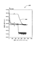
図2は、本発明により形成された(図1Cのような)炭素を含有しないエピタキシャルシード層と、炭素含有エピタキシャル層と、炭素を含有しないエピタキシャルキャップ層のスタックされた層全体の炭素濃度を示すグラフ200である。図2を参照して分かるように、(X軸は、スタックされた層の深さを表し、Y軸は、スタックされた層全体の炭素分布を示す)全体として線202で示される炭素濃度は、スタックされた層の深さ全体に均一に分布する。このようなものとして、本発明のある実施形態によれば、スタックされた層内の炭素濃度は、炭素含有層及び/又はシード層及び/又はキャップ層の相対的な厚さと、炭素含有層内の初期炭素濃度と、を制御することによって、制御することができる。
FIG. 2 illustrates the carbon concentration of the entire stacked layer of carbon-free epitaxial seed layer (such as FIG. 1C), carbon-containing epitaxial layer, and carbon-free epitaxial cap layer formed according to the present invention. This is a
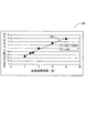
ある実施形態では、最終的な炭素濃度は、炭素を含有しないエピタキシャル層に対する炭素含有エピタキシャル層の相対的な厚さから推定することができる。例えば、図3は、(例えば、図1Cの)シード層とキャップ層の一定の堆積時間の炭素含有エピタキシャル層の堆積時間に対する置換炭素(SC)濃度の依存を示すグラフ300である。図3の線302を参照して分かるように、スタック層内の炭素濃度は、炭素含有エピタキシャル層の堆積時間に比例する。かくして、本発明のある実施形態によれば、シード層/炭素含有層/キャップ層スタック或いは“サンドイッチ”内の炭素濃度は、炭素含有エピタキシャル層の堆積時間を制御することによって制御することができる。
In certain embodiments, the final carbon concentration can be estimated from the relative thickness of the carbon-containing epitaxial layer relative to the carbon-free epitaxial layer. For example, FIG. 3 is a
一つ或いはそれ以上の実施形態では、エピタキシャル層スタックのターゲット炭素濃度は、約200パーツ・パー・ミリオン(ppm)〜約5原子パーセント(at%)、好ましくは約0.5at%〜約2at%の範囲、例えば、約1.5at%であるのがよい。他のターゲット濃度を用いてもよい。ある実施形態では、炭素濃度は、(図1A-図1Dの層104のような)エピタキシャル層で、勾配を有していてもよい。
In one or more embodiments, the target carbon concentration of the epitaxial layer stack is from about 200 parts per million (ppm) to about 5 atomic percent (at%), preferably from about 0.5 at% to about 2 at%. For example, about 1.5 at%. Other target concentrations may be used. In some embodiments, the carbon concentration may be gradient in an epitaxial layer (such as
炭素含有シリコン層に組み込まれる炭素は、シリコン含有層の堆積の直後に、一般的に、結晶格子の格子間位置に配置される。初期炭素濃度は、或いは言い換えれば炭素含有層の堆積されたままの炭素含有量は、約10at%以下、好ましくは約5at%未満、より好ましくは約0.5at%〜約3at%、例えば、約2at%がよい。(連続する)プロセスステップ中のアニーリング(後述する)或いは自然拡散によって、エピタキシャル層は、少なくとも一部、もしそうでないなら全ての格子間炭素が結晶格子の置換位置に組み込まれる。エピタキシャル層スタックの全体の炭素濃度は、格子間或いは置換位置に組み込まれた全ての炭素を含む。高分解能X線回折(XRD)を用いて、置換炭素濃度と厚さを決定することができる。二次イオン質量分析装置(SIMS)を用いて、エピタキシャル層スタックの全体の(置換及び格子間)炭素濃度を決定することができる。置換炭素濃度は、全体の炭素濃度と等しいか或いは低い場合がある。適したアニーリングプロセスは、酸素、窒素、水素、アルゴン、ヘリウム或いはこれらの組み合わせのようなガス雰囲気での高速熱処理(RTP)、レーザアニーリング、或いは熱アニーリングのようなスパイクアニールを含むのがよい。ある実施形態では、アニーリングプロセスは、約800℃〜約1,200℃、好ましくは約1,050℃〜1,100℃の温度で行うのがよい。このようなアニーリングプロセスは、炭素を含有しないキャップ層106が堆積された直後、或いは、他の様々なプロセスステップ(例えば、全体の膜スタックが堆積された後)の直後に行うのがよい。
The carbon that is incorporated into the carbon-containing silicon layer is generally placed in an interstitial position of the crystal lattice immediately after deposition of the silicon-containing layer. The initial carbon concentration, or in other words, the as-deposited carbon content of the carbon-containing layer is about 10 at% or less, preferably less than about 5 at%, more preferably about 0.5 at% to about 3 at%, such as about 2 at% is good. By annealing (described below) or spontaneous diffusion during (successive) process steps, the epitaxial layer is incorporated at least partially, if not all interstitial carbon, at the substitution positions of the crystal lattice. The total carbon concentration of the epitaxial layer stack includes all carbon incorporated in the interstitial or substitutional position. High resolution X-ray diffraction (XRD) can be used to determine the substitutional carbon concentration and thickness. A secondary ion mass spectrometer (SIMS) can be used to determine the total (substitution and interstitial) carbon concentration of the epitaxial layer stack. The substitutional carbon concentration may be equal to or lower than the total carbon concentration. Suitable annealing processes may include spike annealing such as rapid thermal processing (RTP) in a gas atmosphere such as oxygen, nitrogen, hydrogen, argon, helium or combinations thereof, laser annealing, or thermal annealing. In certain embodiments, the annealing process may be performed at a temperature of from about 800 ° C to about 1,200 ° C, preferably from about 1,050 ° C to 1,100 ° C. Such an annealing process may be performed immediately after the carbon-
図4は、本発明によるターゲット炭素濃度を有するエピタキシャル層スタックを形成するための例示的な方法400のフローチャートである。図4を参照して、ステップ401では、基板をプロセスチャンバ内に装填し、約800℃以下の温度まで加熱する。ある実施形態では、750℃未満、700℃未満、或いは650℃未満のような、より低い温度範囲をエピタキシャル膜形成中に用いてもよい。
FIG. 4 is a flowchart of an
ステップ402では、炭素含有エピタキシャル層を基板上に形成する。初期炭素濃度、厚さ及び/又は炭素含有エピタキシャル層の堆積時間は、エピタキシャル層スタックのターゲット炭素濃度に基づいて選択すればよい。その後、ステップ403では、炭素を含有しないエピタキシャル層を、炭素含有エピタキシャル層上に形成する。ある実施形態では、炭素を含有しないエピタキシャル層は、下に横たわる炭素含有層をその後のエッチングから保護するのに十分な厚さである。
In
ステップ404では、HCl及び/又はCl2のようなエッチャントガスを用いて基板をエッチングする。述べたように、炭素を含有しないエピタキシャル層は、下に横たわる炭素含有層をエッチャントガスから保護する。パージステップ(図示せず)を、エッチングの後に行って、いかなるエッチャントガス及び/又は他の望ましくないガスをも使用中のプロセスチャンバから取り除くのがよい。
In
ステップ405では、所望のエピタキシャル層スタック厚さに達しているか決定される。もしそうであれば、ステップ406でプロセスは終了し、さもなければ、プロセスはステップ402に戻り、基板上にエピタキシャル材料を更に堆積させる。
In
他の例示的な実施形態では、プロセスサイクルは、(1)炭素を含有しないシリコン(Si)層堆積ステップ、(2)炭素含有シリコン(SiC)層堆積ステップ、(3)炭素を含有しないシリコン(Si)層堆積ステップ、(4)エッチングステップ、(5)パージステップを含むのがよい。プロセスサイクルを多数回繰り返して、全体のエピタキシャル層スタック厚さを達成することができる。特定の一実施形態では、プロセスサイクルを、約80回繰り返して、エピタキシャル層スタックの約600オングストロームのエピタキシャル材料を得ることができる。この場合、Si或いはSiCの各堆積は、約5〜30オングストロームのエピタキシャル材料を生じ、それらの一部(例えば、約15-25オングストローム)が、後のエッチングステップでエッチング除去される。約80回の繰り返しの後、(例えば、Siモート上に)残存するエピタキシャル材料は、約600オングストロームである場合がある(基板の誘電領域上には殆ど或いは全く堆積していない)。他の実施形態では、約30〜100ナノメートルのエピタキシャル層スタック厚さ範囲を用いるのがよい。 In another exemplary embodiment, the process cycle includes (1) a carbon-free silicon (Si) layer deposition step, (2) a carbon-containing silicon (SiC) layer deposition step, and (3) a carbon-free silicon ( Si) layer deposition step, (4) etching step, and (5) purge step may be included. The process cycle can be repeated many times to achieve the total epitaxial layer stack thickness. In one particular embodiment, the process cycle can be repeated about 80 times to obtain about 600 Angstroms of epitaxial material in the epitaxial layer stack. In this case, each deposition of Si or SiC results in about 5-30 angstroms of epitaxial material, some of which (eg, about 15-25 angstroms) is etched away in a later etching step. After about 80 iterations, the remaining epitaxial material (eg, on the Si mote) may be about 600 angstroms (little or no deposition on the dielectric region of the substrate). In other embodiments, an epitaxial layer stack thickness range of about 30-100 nanometers may be used.
ある実施形態では、エピタキシャル層スタック及び/又は堆積したままのSi:C層の置換炭素濃度範囲は、約0.5-2.0at%である。Si:C層がSi層の間に挟まれているとき、全体のスタック炭素濃度は、Si:C層の厚さと比較したSi層の厚さに依存して減少する。プロセス条件に依存して、置換炭素濃度は、全体の炭素濃度と等しいか或いは低くなる。 In some embodiments, the substitutional carbon concentration range of the epitaxial layer stack and / or as-deposited Si: C layer is about 0.5-2.0 at%. When the Si: C layer is sandwiched between Si layers, the total stack carbon concentration decreases depending on the thickness of the Si layer compared to the thickness of the Si: C layer. Depending on the process conditions, the substitutional carbon concentration is equal to or lower than the total carbon concentration.
例示的なガス流量範囲は、ジクロロシラン、シラン、ジシラン、或いは高級シランの約5-500sccmのシリコン源流量、H2或いはN2の約3-30slmのキャリアガス流量を含む。エッチング中、HClの例示的な流量は、約20-1000sccm、Cl2は約10-500sccmである。 Exemplary gas flow ranges include a silicon source flow rate of about 5-500 sccm for dichlorosilane, silane, disilane, or higher silane, and a carrier gas flow rate of about 3-30 slm for H 2 or N 2 . During etching, an exemplary flow rate of HCl is about 20-1000 sccm and Cl 2 is about 10-500 sccm.
特定の一実施形態では、(パージステップを除く)各プロセスステップ中、ほぼ同じ流量(例えば、約300sccm或いは他の適当な流量)でHClを流すのがよく、エッチングステップ中のみCl2を(例えば、約30sccm或いは他の適当な流速で)流すのがよい。各堆積ステップ中、ジシランを(例えば、約7sccm或いは他の適当な流量で)流すのがよく、Si:C堆積ステップ中メチルシランを(例えば、約2.2sccm或いは他の適当な流量で)流すのがよい。各プロセスサイクルステップ中、N2キャリアガスは、約20slm或いは他の適当な流量で流すのがよく、各パージステップ中、約30slm或いは他の適当な流量まで増加させるのがよい。ある実施形態では、約5オングストロームのSiを第一Si堆積ステップ中(例えば、約4秒で堆積)堆積させ、約9オングストロームのSi:CをSi:C堆積ステップ中堆積(例えば、約7秒で堆積)させるのがよく、約13オングストロームのSiを第二Si堆積ステップ中に堆積(例えば、約10秒で堆積)させるのがよく、約19オングストロームのエピタキシャル材料をエッチングステップ中除去するのがよい(例えば、約13秒のエッチング)。適当なパージ時間を用いることができる(例えば、約10秒)。約600℃のプロセス温度と、堆積とパージ中、約10トール、エッチング中、約13トールのチャンバ圧を用いるのがよい。述べたように、他のプロセス条件を用いてもよい。 In one particular embodiment, HCl may be flowed at approximately the same flow rate (eg, about 300 sccm or other suitable flow rate) during each process step (excluding the purge step), and Cl 2 (eg, only during the etch step) At about 30 sccm or other suitable flow rate). During each deposition step, disilane may be flowed (eg, at about 7 sccm or other suitable flow rate) and during the Si: C deposition step, methylsilane is flowed (eg, at about 2.2 sccm or other suitable flow rate). Is good. During each process cycle step, the N 2 carrier gas may be flowed at about 20 slm or other suitable flow rate and increased to about 30 slm or other suitable flow rate during each purge step. In some embodiments, about 5 Å of Si is deposited during the first Si deposition step (eg, deposition in about 4 seconds) and about 9 Å of Si: C is deposited during the Si: C deposition step (eg, about 7 seconds). About 13 angstroms of Si is deposited during the second Si deposition step (eg, deposition in about 10 seconds), and about 19 angstroms of epitaxial material is removed during the etching step. Good (eg, about 13 seconds of etching). A suitable purge time can be used (eg, about 10 seconds). A process temperature of about 600 ° C. and a chamber pressure of about 10 Torr during deposition and purge and about 13 Torr during etching may be used. As stated, other process conditions may be used.
前述の記載は、本発明の例示的実施形態のみを開示するものである。本発明の範囲内である上記で開示した装置及び方法の変更は、当業者に容易に明らかであろう。従って、本発明は、それの例示的実施形態に関連して開示され、添付した特許請求の範囲によって定められるように、他の実施形態が本発明の精神及び範囲内であることが理解されるべきである。 The foregoing description discloses only exemplary embodiments of the invention. Variations in the apparatus and methods disclosed above that are within the scope of the present invention will be readily apparent to those skilled in the art. Accordingly, it is to be understood that the invention is disclosed in connection with its exemplary embodiments and that other embodiments are within the spirit and scope of the invention as defined by the appended claims. Should.
100…基板、102…エピタキシャル層、104…エピタキシャル層、106…エピタキシャル層、108…エピタキシャル層スタック。
DESCRIPTION OF
Claims (15)
(a)該基板上に、炭素含有シリコンを含む第一シリコン層を形成するステップと、
(b)該第一シリコン層上に、炭素を含有しないシリコンを含む第二シリコン層を形成するステップと、
(c)該第一シリコン層からの炭素を該第二シリコン層に分布させるステップと、
(d)該エピタキシャル層スタックをエッチングして、該第二シリコン層の一部を除去するステップと、
(e)該エッチングされたエピタキシャル層スタックが望ましい厚さになるまで、(a)から(d)のステップを繰り返すステップと、
(f)該第一シリコン層の(i)初期炭素濃度、(ii)厚さ、(iii)堆積時間の一つ以上を制御して、該エッチングされたエピタキシャル層スタックのターゲット炭素濃度を達成するステップと、
を含む、前記方法。A method of forming an epitaxial layer stack having a desired thickness and target carbon concentration on a substrate, comprising:
(A) forming a first silicon layer containing carbon-containing silicon on the substrate;
(B) forming a second silicon layer containing silicon not containing carbon on the first silicon layer;
(C) distributing carbon from the first silicon layer to the second silicon layer;
(D) etching the epitaxial layer stack to remove a portion of the second silicon layer;
(E) repeating steps (a) to (d) until the etched epitaxial layer stack has the desired thickness;
(F) controlling one or more of (i) initial carbon concentration, (ii) thickness, and (iii) deposition time of the first silicon layer to achieve a target carbon concentration of the etched epitaxial layer stack. Steps,
Said method.
該エピタキシャル層スタックの望ましい炭素濃度を決定するステップと、
エピタキシャル層スタックを、
(a)該基板上に、炭素を含む第一エピタキシャル層を形成し、
(b)該第一エピタキシャル層上に、炭素を含有しないキャップ層を形成し、
(c)該第一エピタキシャル層からの炭素を該キャップ層に分布させ、
(d)エッチングして該キャップ層の一部を除去し、
(e)該エッチングされたエピタキシャル層スタックが望ましい厚さになるまで、(a)から(d)のステップを繰り返し、
(f)該第一エピタキシャル層の(i)初期炭素濃度、(ii)厚さ、(iii)堆積時間の一つ以上を制御して、該エッチングされたエピタキシャル層スタックのターゲット炭素濃度を達成する
ことによって形成するステップと、
を含む、前記方法。A method for controlling the carbon concentration of an epitaxial layer stack formed on a substrate, comprising:
Determining a desired carbon concentration of the epitaxial layer stack;
Epitaxial layer stack,
(A) forming a first epitaxial layer containing carbon on the substrate;
(B) forming a cap layer not containing carbon on the first epitaxial layer;
(C) distributing carbon from the first epitaxial layer to the cap layer;
(D) etching to remove a portion of the cap layer;
(E) repeating steps (a) to (d) until the etched epitaxial layer stack has the desired thickness;
(F) controlling one or more of (i) initial carbon concentration, (ii) thickness, and (iii) deposition time of the first epitaxial layer to achieve a target carbon concentration of the etched epitaxial layer stack. Forming a step,
Said method.
Applications Claiming Priority (3)
| Application Number | Priority Date | Filing Date | Title |
|---|---|---|---|
| US83477306P | 2006-07-31 | 2006-07-31 | |
| US60/834,773 | 2006-07-31 | ||
| PCT/US2007/017193 WO2008016650A2 (en) | 2006-07-31 | 2007-07-31 | Methods of forming carbon-containing silicon epitaxial layers |
Publications (3)
| Publication Number | Publication Date |
|---|---|
| JP2009545886A JP2009545886A (en) | 2009-12-24 |
| JP2009545886A5 JP2009545886A5 (en) | 2012-02-16 |
| JP5090451B2 true JP5090451B2 (en) | 2012-12-05 |
Family
ID=38997702
Family Applications (1)
| Application Number | Title | Priority Date | Filing Date |
|---|---|---|---|
| JP2009522864A Expired - Fee Related JP5090451B2 (en) | 2006-07-31 | 2007-07-31 | Method for forming carbon-containing silicon epitaxial layer |
Country Status (7)
| Country | Link |
|---|---|
| US (1) | US8029620B2 (en) |
| JP (1) | JP5090451B2 (en) |
| KR (1) | KR101160930B1 (en) |
| CN (2) | CN101496153A (en) |
| DE (1) | DE112007001814T5 (en) |
| TW (1) | TWI379347B (en) |
| WO (1) | WO2008016650A2 (en) |
Cited By (1)
| Publication number | Priority date | Publication date | Assignee | Title |
|---|---|---|---|---|
| WO2023243342A1 (en) * | 2022-06-17 | 2023-12-21 | 信越半導体株式会社 | Semiconductor wafer manufacturing method and semiconductor wafer |
Families Citing this family (56)
| Publication number | Priority date | Publication date | Assignee | Title |
|---|---|---|---|---|
| US7682940B2 (en) * | 2004-12-01 | 2010-03-23 | Applied Materials, Inc. | Use of Cl2 and/or HCl during silicon epitaxial film formation |
| WO2007112058A2 (en) * | 2006-03-24 | 2007-10-04 | Applied Materials, Inc. | Carbon precursors for use during silicon epitaxial firm formation |
| DE112007001814T5 (en) * | 2006-07-31 | 2009-06-04 | Applied Materials, Inc., Santa Clara | A method of forming carbonaceous silicon epitaxial layers |
| US7588980B2 (en) * | 2006-07-31 | 2009-09-15 | Applied Materials, Inc. | Methods of controlling morphology during epitaxial layer formation |
| US8273617B2 (en) | 2009-09-30 | 2012-09-25 | Suvolta, Inc. | Electronic devices and systems, and methods for making and using the same |
| US8421162B2 (en) | 2009-09-30 | 2013-04-16 | Suvolta, Inc. | Advanced transistors with punch through suppression |
| US8530286B2 (en) | 2010-04-12 | 2013-09-10 | Suvolta, Inc. | Low power semiconductor transistor structure and method of fabrication thereof |
| US8569128B2 (en) | 2010-06-21 | 2013-10-29 | Suvolta, Inc. | Semiconductor structure and method of fabrication thereof with mixed metal types |
| US8759872B2 (en) | 2010-06-22 | 2014-06-24 | Suvolta, Inc. | Transistor with threshold voltage set notch and method of fabrication thereof |
| US8685845B2 (en) * | 2010-08-20 | 2014-04-01 | International Business Machines Corporation | Epitaxial growth of silicon doped with carbon and phosphorus using hydrogen carrier gas |
| CN102386067B (en) * | 2010-08-31 | 2013-12-18 | 中国科学院上海微系统与信息技术研究所 | Epitaxial growth method for effectively restraining self-doping effect |
| US8404551B2 (en) | 2010-12-03 | 2013-03-26 | Suvolta, Inc. | Source/drain extension control for advanced transistors |
| WO2012102755A1 (en) | 2011-01-28 | 2012-08-02 | Applied Materials, Inc. | Carbon addition for low resistivity in situ doped silicon epitaxy |
| US8461875B1 (en) | 2011-02-18 | 2013-06-11 | Suvolta, Inc. | Digital circuits having improved transistors, and methods therefor |
| US8525271B2 (en) | 2011-03-03 | 2013-09-03 | Suvolta, Inc. | Semiconductor structure with improved channel stack and method for fabrication thereof |
| US8748270B1 (en) | 2011-03-30 | 2014-06-10 | Suvolta, Inc. | Process for manufacturing an improved analog transistor |
| US8796048B1 (en) | 2011-05-11 | 2014-08-05 | Suvolta, Inc. | Monitoring and measurement of thin film layers |
| US8999861B1 (en) | 2011-05-11 | 2015-04-07 | Suvolta, Inc. | Semiconductor structure with substitutional boron and method for fabrication thereof |
| US8811068B1 (en) | 2011-05-13 | 2014-08-19 | Suvolta, Inc. | Integrated circuit devices and methods |
| US8569156B1 (en) | 2011-05-16 | 2013-10-29 | Suvolta, Inc. | Reducing or eliminating pre-amorphization in transistor manufacture |
| US8735987B1 (en) | 2011-06-06 | 2014-05-27 | Suvolta, Inc. | CMOS gate stack structures and processes |
| US8995204B2 (en) | 2011-06-23 | 2015-03-31 | Suvolta, Inc. | Circuit devices and methods having adjustable transistor body bias |
| US8629016B1 (en) | 2011-07-26 | 2014-01-14 | Suvolta, Inc. | Multiple transistor types formed in a common epitaxial layer by differential out-diffusion from a doped underlayer |
| EP2555235B1 (en) | 2011-08-02 | 2014-06-18 | Nxp B.V. | Method of manufacturing an IC comprising a plurality of bipolar transistors and IC comprising a plurality of bipolar transistors |
| US8748986B1 (en) | 2011-08-05 | 2014-06-10 | Suvolta, Inc. | Electronic device with controlled threshold voltage |
| KR101891373B1 (en) | 2011-08-05 | 2018-08-24 | 엠아이이 후지쯔 세미컨덕터 리미티드 | Semiconductor devices having fin structures and fabrication methods thereof |
| US8614128B1 (en) | 2011-08-23 | 2013-12-24 | Suvolta, Inc. | CMOS structures and processes based on selective thinning |
| US8645878B1 (en) | 2011-08-23 | 2014-02-04 | Suvolta, Inc. | Porting a circuit design from a first semiconductor process to a second semiconductor process |
| US8713511B1 (en) | 2011-09-16 | 2014-04-29 | Suvolta, Inc. | Tools and methods for yield-aware semiconductor manufacturing process target generation |
| JP5741382B2 (en) | 2011-09-30 | 2015-07-01 | 東京エレクトロン株式会社 | Thin film forming method and film forming apparatus |
| US9236466B1 (en) | 2011-10-07 | 2016-01-12 | Mie Fujitsu Semiconductor Limited | Analog circuits having improved insulated gate transistors, and methods therefor |
| US8895327B1 (en) | 2011-12-09 | 2014-11-25 | Suvolta, Inc. | Tipless transistors, short-tip transistors, and methods and circuits therefor |
| US8819603B1 (en) | 2011-12-15 | 2014-08-26 | Suvolta, Inc. | Memory circuits and methods of making and designing the same |
| US8883600B1 (en) | 2011-12-22 | 2014-11-11 | Suvolta, Inc. | Transistor having reduced junction leakage and methods of forming thereof |
| US8599623B1 (en) | 2011-12-23 | 2013-12-03 | Suvolta, Inc. | Circuits and methods for measuring circuit elements in an integrated circuit device |
| US8970289B1 (en) | 2012-01-23 | 2015-03-03 | Suvolta, Inc. | Circuits and devices for generating bi-directional body bias voltages, and methods therefor |
| US8877619B1 (en) | 2012-01-23 | 2014-11-04 | Suvolta, Inc. | Process for manufacture of integrated circuits with different channel doping transistor architectures and devices therefrom |
| US9093550B1 (en) | 2012-01-31 | 2015-07-28 | Mie Fujitsu Semiconductor Limited | Integrated circuits having a plurality of high-K metal gate FETs with various combinations of channel foundation structure and gate stack structure and methods of making same |
| US9406567B1 (en) | 2012-02-28 | 2016-08-02 | Mie Fujitsu Semiconductor Limited | Method for fabricating multiple transistor devices on a substrate with varying threshold voltages |
| JP5792101B2 (en) * | 2012-03-15 | 2015-10-07 | 東京エレクトロン株式会社 | Method for forming laminated semiconductor film |
| US8863064B1 (en) | 2012-03-23 | 2014-10-14 | Suvolta, Inc. | SRAM cell layout structure and devices therefrom |
| US9299698B2 (en) | 2012-06-27 | 2016-03-29 | Mie Fujitsu Semiconductor Limited | Semiconductor structure with multiple transistors having various threshold voltages |
| US8637955B1 (en) | 2012-08-31 | 2014-01-28 | Suvolta, Inc. | Semiconductor structure with reduced junction leakage and method of fabrication thereof |
| US9112057B1 (en) | 2012-09-18 | 2015-08-18 | Mie Fujitsu Semiconductor Limited | Semiconductor devices with dopant migration suppression and method of fabrication thereof |
| US9041126B2 (en) | 2012-09-21 | 2015-05-26 | Mie Fujitsu Semiconductor Limited | Deeply depleted MOS transistors having a screening layer and methods thereof |
| CN104854698A (en) | 2012-10-31 | 2015-08-19 | 三重富士通半导体有限责任公司 | Dram-type device with low variation transistor peripheral circuits, and related methods |
| US8816754B1 (en) | 2012-11-02 | 2014-08-26 | Suvolta, Inc. | Body bias circuits and methods |
| US9093997B1 (en) | 2012-11-15 | 2015-07-28 | Mie Fujitsu Semiconductor Limited | Slew based process and bias monitors and related methods |
| US9070477B1 (en) | 2012-12-12 | 2015-06-30 | Mie Fujitsu Semiconductor Limited | Bit interleaved low voltage static random access memory (SRAM) and related methods |
| US9112484B1 (en) | 2012-12-20 | 2015-08-18 | Mie Fujitsu Semiconductor Limited | Integrated circuit process and bias monitors and related methods |
| US9268885B1 (en) | 2013-02-28 | 2016-02-23 | Mie Fujitsu Semiconductor Limited | Integrated circuit device methods and models with predicted device metric variations |
| US9299801B1 (en) | 2013-03-14 | 2016-03-29 | Mie Fujitsu Semiconductor Limited | Method for fabricating a transistor device with a tuned dopant profile |
| US9478571B1 (en) | 2013-05-24 | 2016-10-25 | Mie Fujitsu Semiconductor Limited | Buried channel deeply depleted channel transistor |
| US9710006B2 (en) | 2014-07-25 | 2017-07-18 | Mie Fujitsu Semiconductor Limited | Power up body bias circuits and methods |
| US9319013B2 (en) | 2014-08-19 | 2016-04-19 | Mie Fujitsu Semiconductor Limited | Operational amplifier input offset correction with transistor threshold voltage adjustment |
| CN107731735B (en) * | 2017-11-21 | 2020-02-14 | 长江存储科技有限责任公司 | SEG preparation process for improving SEG growth form through mild wet etching |
Family Cites Families (181)
| Publication number | Priority date | Publication date | Assignee | Title |
|---|---|---|---|---|
| US3675619A (en) | 1969-02-25 | 1972-07-11 | Monsanto Co | Apparatus for production of epitaxial films |
| NL187942C (en) | 1980-08-18 | 1992-02-17 | Philips Nv | ZENERDIODE AND METHOD OF MANUFACTURE THEREOF |
| US5693139A (en) | 1984-07-26 | 1997-12-02 | Research Development Corporation Of Japan | Growth of doped semiconductor monolayers |
| US5294286A (en) | 1984-07-26 | 1994-03-15 | Research Development Corporation Of Japan | Process for forming a thin film of silicon |
| JPS62243144A (en) * | 1986-04-15 | 1987-10-23 | Dainippon Printing Co Ltd | Optical recording medium and optical recording method |
| JPH0639357B2 (en) | 1986-09-08 | 1994-05-25 | 新技術開発事業団 | Method for growing element semiconductor single crystal thin film |
| US5607511A (en) | 1992-02-21 | 1997-03-04 | International Business Machines Corporation | Method and apparatus for low temperature, low pressure chemical vapor deposition of epitaxial silicon layers |
| US4865659A (en) * | 1986-11-27 | 1989-09-12 | Sharp Kabushiki Kaisha | Heteroepitaxial growth of SiC on Si |
| US5112439A (en) | 1988-11-30 | 1992-05-12 | Mcnc | Method for selectively depositing material on substrates |
| JPH0824191B2 (en) | 1989-03-17 | 1996-03-06 | 富士通株式会社 | Thin film transistor |
| EP0413982B1 (en) | 1989-07-27 | 1997-05-14 | Junichi Nishizawa | Impurity doping method with adsorbed diffusion source |
| US5112429A (en) * | 1990-08-17 | 1992-05-12 | Costas Dan N | Labeling apparatus |
| JP2880322B2 (en) | 1991-05-24 | 1999-04-05 | キヤノン株式会社 | Method of forming deposited film |
| WO1992022922A2 (en) * | 1991-06-12 | 1992-12-23 | Case Western Reserve University | Process for the controlled growth of single-crystal films of silicon carbide polytypes on silicon carbide wafers |
| US5227330A (en) | 1991-10-31 | 1993-07-13 | International Business Machines Corporation | Comprehensive process for low temperature SI epit axial growth |
| JPH05175141A (en) * | 1991-12-26 | 1993-07-13 | Fujitsu Ltd | Vapor-phase epitaxial growth apparatus and method |
| US5480818A (en) | 1992-02-10 | 1996-01-02 | Fujitsu Limited | Method for forming a film and method for manufacturing a thin film transistor |
| JP2917694B2 (en) | 1992-04-02 | 1999-07-12 | 日本電気株式会社 | Compound semiconductor vapor deposition method and apparatus therefor |
| JPH0750690B2 (en) | 1992-08-21 | 1995-05-31 | 日本電気株式会社 | Method and apparatus for epitaxial growth of semiconductor crystal using halide |
| US5273930A (en) | 1992-09-03 | 1993-12-28 | Motorola, Inc. | Method of forming a non-selective silicon-germanium epitaxial film |
| US5236545A (en) * | 1992-10-05 | 1993-08-17 | The Board Of Governors Of Wayne State University | Method for heteroepitaxial diamond film development |
| JP3255469B2 (en) | 1992-11-30 | 2002-02-12 | 三菱電機株式会社 | Laser thin film forming equipment |
| JP3265042B2 (en) | 1993-03-18 | 2002-03-11 | 東京エレクトロン株式会社 | Film formation method |
| JPH0729897A (en) | 1993-06-25 | 1995-01-31 | Nec Corp | Manufacture of semiconductor device |
| US5372860A (en) | 1993-07-06 | 1994-12-13 | Corning Incorporated | Silicon device production |
| JPH07109573A (en) | 1993-10-12 | 1995-04-25 | Semiconductor Energy Lab Co Ltd | Glass substrate and heat treatment |
| US5796116A (en) | 1994-07-27 | 1998-08-18 | Sharp Kabushiki Kaisha | Thin-film semiconductor device including a semiconductor film with high field-effect mobility |
| WO1996015550A1 (en) * | 1994-11-10 | 1996-05-23 | Lawrence Semiconductor Research Laboratory, Inc. | Silicon-germanium-carbon compositions and processes thereof |
| JPH08288215A (en) * | 1995-04-17 | 1996-11-01 | Nippon Steel Corp | Manufacture of semiconductor substrate and semiconductor substrate |
| US6342277B1 (en) | 1996-08-16 | 2002-01-29 | Licensee For Microelectronics: Asm America, Inc. | Sequential chemical vapor deposition |
| US5916365A (en) | 1996-08-16 | 1999-06-29 | Sherman; Arthur | Sequential chemical vapor deposition |
| US5807792A (en) | 1996-12-18 | 1998-09-15 | Siemens Aktiengesellschaft | Uniform distribution of reactants in a device layer |
| US6335280B1 (en) | 1997-01-13 | 2002-01-01 | Asm America, Inc. | Tungsten silicide deposition process |
| US6055927A (en) | 1997-01-14 | 2000-05-02 | Applied Komatsu Technology, Inc. | Apparatus and method for white powder reduction in silicon nitride deposition using remote plasma source cleaning technology |
| JP2953567B2 (en) * | 1997-02-06 | 1999-09-27 | 日本電気株式会社 | Method for manufacturing semiconductor device |
| US5849092A (en) | 1997-02-25 | 1998-12-15 | Applied Materials, Inc. | Process for chlorine trifluoride chamber cleaning |
| US6022587A (en) | 1997-05-13 | 2000-02-08 | Applied Materials, Inc. | Method and apparatus for improving film deposition uniformity on a substrate |
| TW417249B (en) | 1997-05-14 | 2001-01-01 | Applied Materials Inc | Reliability barrier integration for cu application |
| US6118216A (en) | 1997-06-02 | 2000-09-12 | Osram Sylvania Inc. | Lead and arsenic free borosilicate glass and lamp containing same |
| US6287965B1 (en) | 1997-07-28 | 2001-09-11 | Samsung Electronics Co, Ltd. | Method of forming metal layer using atomic layer deposition and semiconductor device having the metal layer as barrier metal layer or upper or lower electrode of capacitor |
| KR100385946B1 (en) | 1999-12-08 | 2003-06-02 | 삼성전자주식회사 | Method for forming a metal layer by an atomic layer deposition and a semiconductor device with the metal layer as a barrier metal layer, an upper electrode, or a lower electrode of capacitor |
| KR100269306B1 (en) | 1997-07-31 | 2000-10-16 | 윤종용 | Integrate circuit device having buffer layer containing metal oxide stabilized by low temperature treatment and fabricating method thereof |
| KR100261017B1 (en) | 1997-08-19 | 2000-08-01 | 윤종용 | Method for forming metal wiring of semiconductor device |
| US6019838A (en) * | 1998-01-05 | 2000-02-01 | Memc Electronic Materials, Inc. | Crystal growing apparatus with melt-doping facility |
| US6042654A (en) | 1998-01-13 | 2000-03-28 | Applied Materials, Inc. | Method of cleaning CVD cold-wall chamber and exhaust lines |
| TW437017B (en) | 1998-02-05 | 2001-05-28 | Asm Japan Kk | Silicone polymer insulation film on semiconductor substrate and method for formation thereof |
| US6514880B2 (en) | 1998-02-05 | 2003-02-04 | Asm Japan K.K. | Siloxan polymer film on semiconductor substrate and method for forming same |
| US6383955B1 (en) | 1998-02-05 | 2002-05-07 | Asm Japan K.K. | Silicone polymer insulation film on semiconductor substrate and method for forming the film |
| US6797558B2 (en) | 2001-04-24 | 2004-09-28 | Micron Technology, Inc. | Methods of forming a capacitor with substantially selective deposite of polysilicon on a substantially crystalline capacitor dielectric layer |
| US6159852A (en) | 1998-02-13 | 2000-12-12 | Micron Technology, Inc. | Method of depositing polysilicon, method of fabricating a field effect transistor, method of forming a contact to a substrate, method of forming a capacitor |
| EP1060287B1 (en) | 1998-03-06 | 2005-01-26 | ASM America, Inc. | Method of depositing silicon with high step coverage |
| US6019839A (en) | 1998-04-17 | 2000-02-01 | Applied Materials, Inc. | Method and apparatus for forming an epitaxial titanium silicide film by low pressure chemical vapor deposition |
| JP4214585B2 (en) | 1998-04-24 | 2009-01-28 | 富士ゼロックス株式会社 | Semiconductor device, semiconductor device manufacturing method and manufacturing apparatus |
| US6025627A (en) | 1998-05-29 | 2000-02-15 | Micron Technology, Inc. | Alternate method and structure for improved floating gate tunneling devices |
| FR2779572B1 (en) | 1998-06-05 | 2003-10-17 | St Microelectronics Sa | LOW NOISE VERTICAL BIPOLAR TRANSISTOR AND MANUFACTURING METHOD THEREOF |
| KR100275738B1 (en) | 1998-08-07 | 2000-12-15 | 윤종용 | Method for producing thin film using atomatic layer deposition |
| JP4204671B2 (en) | 1998-09-11 | 2009-01-07 | 三菱電機株式会社 | Manufacturing method of semiconductor device |
| KR100287180B1 (en) | 1998-09-17 | 2001-04-16 | 윤종용 | Method for manufacturing semiconductor device including metal interconnection formed using interface control layer |
| KR100327328B1 (en) | 1998-10-13 | 2002-05-09 | 윤종용 | Method for forming dielectric layer of capacitor having partially different thickness in the layer |
| JP3516623B2 (en) * | 1999-01-14 | 2004-04-05 | 松下電器産業株式会社 | Manufacturing method of semiconductor crystal |
| JP3723396B2 (en) * | 1999-02-23 | 2005-12-07 | サンゴバン・ティーエム株式会社 | High purity crystalline inorganic fiber and method for producing the same |
| US6305314B1 (en) | 1999-03-11 | 2001-10-23 | Genvs, Inc. | Apparatus and concept for minimizing parasitic chemical vapor deposition during atomic layer deposition |
| US6200893B1 (en) | 1999-03-11 | 2001-03-13 | Genus, Inc | Radical-assisted sequential CVD |
| JP4556329B2 (en) | 1999-04-20 | 2010-10-06 | ソニー株式会社 | Thin film forming equipment |
| US20030232554A1 (en) | 1999-05-04 | 2003-12-18 | Blum Ronald D. | Multi-layer tacky and water-absorbing shoe-cleaning product |
| US6124158A (en) | 1999-06-08 | 2000-09-26 | Lucent Technologies Inc. | Method of reducing carbon contamination of a thin dielectric film by using gaseous organic precursors, inert gas, and ozone to react with carbon contaminants |
| KR20010017820A (en) | 1999-08-14 | 2001-03-05 | 윤종용 | Semiconductor device and manufacturing method thereof |
| US6391785B1 (en) | 1999-08-24 | 2002-05-21 | Interuniversitair Microelektronica Centrum (Imec) | Method for bottomless deposition of barrier layers in integrated circuit metallization schemes |
| US6511539B1 (en) | 1999-09-08 | 2003-01-28 | Asm America, Inc. | Apparatus and method for growth of a thin film |
| US6489241B1 (en) | 1999-09-17 | 2002-12-03 | Applied Materials, Inc. | Apparatus and method for surface finishing a silicon film |
| DE10049257B4 (en) | 1999-10-06 | 2015-05-13 | Samsung Electronics Co., Ltd. | Process for thin film production by means of atomic layer deposition |
| FI117942B (en) | 1999-10-14 | 2007-04-30 | Asm Int | Process for making oxide thin films |
| TW468212B (en) | 1999-10-25 | 2001-12-11 | Motorola Inc | Method for fabricating a semiconductor structure including a metal oxide interface with silicon |
| FR2801420B1 (en) | 1999-11-23 | 2002-04-12 | St Microelectronics Sa | LOW FREQUENCY LOW NOISE VERTICAL BIPOLAR TRANSISTOR AND HIGH CURRENT GAIN, AND MANUFACTURING METHOD THEREOF |
| US6780704B1 (en) | 1999-12-03 | 2004-08-24 | Asm International Nv | Conformal thin films over textured capacitor electrodes |
| FI118804B (en) | 1999-12-03 | 2008-03-31 | Asm Int | Process for making oxide films |
| US6291319B1 (en) | 1999-12-17 | 2001-09-18 | Motorola, Inc. | Method for fabricating a semiconductor structure having a stable crystalline interface with silicon |
| US6348420B1 (en) | 1999-12-23 | 2002-02-19 | Asm America, Inc. | Situ dielectric stacks |
| EP1123991A3 (en) | 2000-02-08 | 2002-11-13 | Asm Japan K.K. | Low dielectric constant materials and processes |
| US6492283B2 (en) | 2000-02-22 | 2002-12-10 | Asm Microchemistry Oy | Method of forming ultrathin oxide layer |
| AU2001245388A1 (en) | 2000-03-07 | 2001-09-17 | Asm America, Inc. | Graded thin films |
| KR100363088B1 (en) | 2000-04-20 | 2002-12-02 | 삼성전자 주식회사 | Method of manufacturing barrier metal layer using atomic layer deposition method |
| US6630413B2 (en) | 2000-04-28 | 2003-10-07 | Asm Japan K.K. | CVD syntheses of silicon nitride materials |
| US6458718B1 (en) | 2000-04-28 | 2002-10-01 | Asm Japan K.K. | Fluorine-containing materials and processes |
| EP2293322A1 (en) | 2000-06-08 | 2011-03-09 | Genitech, Inc. | Method for forming a metal nitride layer |
| KR100373853B1 (en) | 2000-08-11 | 2003-02-26 | 삼성전자주식회사 | Selective epitaxial growth method in semiconductor device |
| US6461909B1 (en) | 2000-08-30 | 2002-10-08 | Micron Technology, Inc. | Process for fabricating RuSixOy-containing adhesion layers |
| US20020163013A1 (en) | 2000-09-11 | 2002-11-07 | Kenji Toyoda | Heterojunction bipolar transistor |
| US6969539B2 (en) | 2000-09-28 | 2005-11-29 | President And Fellows Of Harvard College | Vapor deposition of metal oxides, silicates and phosphates, and silicon dioxide |
| KR100378186B1 (en) | 2000-10-19 | 2003-03-29 | 삼성전자주식회사 | Semiconductor device adopting thin film formed by atomic layer deposition and fabrication method thereof |
| US6613695B2 (en) | 2000-11-24 | 2003-09-02 | Asm America, Inc. | Surface preparation prior to deposition |
| AU2002225761A1 (en) | 2000-11-30 | 2002-06-11 | Asm America, Inc. | Thin films for magnetic devices |
| KR100385947B1 (en) | 2000-12-06 | 2003-06-02 | 삼성전자주식회사 | Method of forming thin film by atomic layer deposition |
| KR20020049875A (en) | 2000-12-20 | 2002-06-26 | 윤종용 | Ferroelectric capacitor in semiconductor memory device and method for manufacturing the same |
| JP2002198525A (en) | 2000-12-27 | 2002-07-12 | Toshiba Corp | Semiconductor device and its manufacturing method |
| KR100393208B1 (en) | 2001-01-15 | 2003-07-31 | 삼성전자주식회사 | Semiconductor device using doped polycrystalline silicon-germanium layer and method for manufacturing the same |
| US6426265B1 (en) | 2001-01-30 | 2002-07-30 | International Business Machines Corporation | Incorporation of carbon in silicon/silicon germanium epitaxial layer to enhance yield for Si-Ge bipolar technology |
| US6528374B2 (en) | 2001-02-05 | 2003-03-04 | International Business Machines Corporation | Method for forming dielectric stack without interfacial layer |
| KR101050377B1 (en) | 2001-02-12 | 2011-07-20 | 에이에스엠 아메리카, 인코포레이티드 | Improved process for deposition of semiconductor films |
| US7026219B2 (en) | 2001-02-12 | 2006-04-11 | Asm America, Inc. | Integration of high k gate dielectric |
| US20020117399A1 (en) | 2001-02-23 | 2002-08-29 | Applied Materials, Inc. | Atomically thin highly resistive barrier layer in a copper via |
| JP3547419B2 (en) | 2001-03-13 | 2004-07-28 | 株式会社東芝 | Semiconductor device and manufacturing method thereof |
| US6812101B2 (en) | 2001-04-02 | 2004-11-02 | Matsushita Electric Industrial Co., Ltd. | Semiconductor device and method for manufacture thereof |
| US6576535B2 (en) * | 2001-04-11 | 2003-06-10 | Texas Instruments Incorporated | Carbon doped epitaxial layer for high speed CB-CMOS |
| US6750119B2 (en) * | 2001-04-20 | 2004-06-15 | International Business Machines Corporation | Epitaxial and polycrystalline growth of Si1-x-yGexCy and Si1-yCy alloy layers on Si by UHV-CVD |
| JP2002343790A (en) | 2001-05-21 | 2002-11-29 | Nec Corp | Vapor-phase deposition method of metallic compound thin film and method for manufacturing semiconductor device |
| TWI307912B (en) | 2001-05-30 | 2009-03-21 | Asm Inc | Low temperature load and bake |
| US6828218B2 (en) | 2001-05-31 | 2004-12-07 | Samsung Electronics Co., Ltd. | Method of forming a thin film using atomic layer deposition |
| US6391803B1 (en) | 2001-06-20 | 2002-05-21 | Samsung Electronics Co., Ltd. | Method of forming silicon containing thin films by atomic layer deposition utilizing trisdimethylaminosilane |
| US6861334B2 (en) | 2001-06-21 | 2005-03-01 | Asm International, N.V. | Method of fabricating trench isolation structures for integrated circuits using atomic layer deposition |
| US6709989B2 (en) | 2001-06-21 | 2004-03-23 | Motorola, Inc. | Method for fabricating a semiconductor structure including a metal oxide interface with silicon |
| US20030198754A1 (en) | 2001-07-16 | 2003-10-23 | Ming Xi | Aluminum oxide chamber and process |
| US20030066486A1 (en) | 2001-08-30 | 2003-04-10 | Applied Materials, Inc. | Microwave heat shield for plasma chamber |
| US6806145B2 (en) | 2001-08-31 | 2004-10-19 | Asm International, N.V. | Low temperature method of forming a gate stack with a high k layer deposited over an interfacial oxide layer |
| US6960537B2 (en) | 2001-10-02 | 2005-11-01 | Asm America, Inc. | Incorporation of nitrogen into high k dielectric film |
| US20030072884A1 (en) | 2001-10-15 | 2003-04-17 | Applied Materials, Inc. | Method of titanium and titanium nitride layer deposition |
| US6916398B2 (en) | 2001-10-26 | 2005-07-12 | Applied Materials, Inc. | Gas delivery apparatus and method for atomic layer deposition |
| KR20030035152A (en) * | 2001-10-30 | 2003-05-09 | 주식회사 하이닉스반도체 | Method for fabricating semiconductor wafer |
| US6743681B2 (en) | 2001-11-09 | 2004-06-01 | Micron Technology, Inc. | Methods of Fabricating Gate and Storage Dielectric Stacks having Silicon-Rich-Nitride |
| US6590344B2 (en) | 2001-11-20 | 2003-07-08 | Taiwan Semiconductor Manufacturing Co., Ltd. | Selectively controllable gas feed zones for a plasma reactor |
| US6551893B1 (en) | 2001-11-27 | 2003-04-22 | Micron Technology, Inc. | Atomic layer deposition of capacitor dielectric |
| US6773507B2 (en) | 2001-12-06 | 2004-08-10 | Applied Materials, Inc. | Apparatus and method for fast-cycle atomic layer deposition |
| US7081271B2 (en) | 2001-12-07 | 2006-07-25 | Applied Materials, Inc. | Cyclical deposition of refractory metal silicon nitride |
| WO2003060982A2 (en) * | 2001-12-21 | 2003-07-24 | Memc Electronic Materials, Inc. | Ideal oxygen precipitating silicon wafers with nitrogen/carbon stabilized oxygen precipitate nucleation centers and process for making the same |
| US6696332B2 (en) | 2001-12-26 | 2004-02-24 | Texas Instruments Incorporated | Bilayer deposition to avoid unwanted interfacial reactions during high K gate dielectric processing |
| US6790755B2 (en) | 2001-12-27 | 2004-09-14 | Advanced Micro Devices, Inc. | Preparation of stack high-K gate dielectrics with nitrided layer |
| US6620670B2 (en) | 2002-01-18 | 2003-09-16 | Applied Materials, Inc. | Process conditions and precursors for atomic layer deposition (ALD) of AL2O3 |
| WO2003065424A2 (en) | 2002-01-25 | 2003-08-07 | Applied Materials, Inc. | Apparatus for cyclical deposition of thin films |
| US6911391B2 (en) | 2002-01-26 | 2005-06-28 | Applied Materials, Inc. | Integration of titanium and titanium nitride layers |
| JP3914064B2 (en) | 2002-02-28 | 2007-05-16 | 富士通株式会社 | Method and apparatus for growing mixed crystal film |
| US20030216981A1 (en) | 2002-03-12 | 2003-11-20 | Michael Tillman | Method and system for hosting centralized online point-of-sale activities for a plurality of distributed customers and vendors |
| US6825134B2 (en) | 2002-03-26 | 2004-11-30 | Applied Materials, Inc. | Deposition of film layers by alternately pulsing a precursor and high frequency power in a continuous gas flow |
| JP3937892B2 (en) | 2002-04-01 | 2007-06-27 | 日本電気株式会社 | Thin film forming method and semiconductor device manufacturing method |
| US7439191B2 (en) | 2002-04-05 | 2008-10-21 | Applied Materials, Inc. | Deposition of silicon layers for active matrix liquid crystal display (AMLCD) applications |
| US6846516B2 (en) | 2002-04-08 | 2005-01-25 | Applied Materials, Inc. | Multiple precursor cyclical deposition system |
| US6720027B2 (en) | 2002-04-08 | 2004-04-13 | Applied Materials, Inc. | Cyclical deposition of a variable content titanium silicon nitride layer |
| US6869838B2 (en) | 2002-04-09 | 2005-03-22 | Applied Materials, Inc. | Deposition of passivation layers for active matrix liquid crystal display (AMLCD) applications |
| US20030235961A1 (en) | 2002-04-17 | 2003-12-25 | Applied Materials, Inc. | Cyclical sequential deposition of multicomponent films |
| US20030213560A1 (en) | 2002-05-16 | 2003-11-20 | Yaxin Wang | Tandem wafer processing system and process |
| US20030215570A1 (en) | 2002-05-16 | 2003-11-20 | Applied Materials, Inc. | Deposition of silicon nitride |
| US6716719B2 (en) | 2002-05-29 | 2004-04-06 | Micron Technology, Inc. | Method of forming biasable isolation regions using epitaxially grown silicon between the isolation regions |
| US7105891B2 (en) | 2002-07-15 | 2006-09-12 | Texas Instruments Incorporated | Gate structure and method |
| US6723658B2 (en) | 2002-07-15 | 2004-04-20 | Texas Instruments Incorporated | Gate structure and method |
| US7449385B2 (en) | 2002-07-26 | 2008-11-11 | Texas Instruments Incorporated | Gate dielectric and method |
| US6919251B2 (en) | 2002-07-31 | 2005-07-19 | Texas Instruments Incorporated | Gate dielectric and method |
| US7186630B2 (en) | 2002-08-14 | 2007-03-06 | Asm America, Inc. | Deposition of amorphous silicon-containing films |
| KR100542736B1 (en) | 2002-08-17 | 2006-01-11 | 삼성전자주식회사 | Method of forming oxide layer using atomic layer deposition method and method of forming capacitor of semiconductor device using the same |
| US7199023B2 (en) | 2002-08-28 | 2007-04-03 | Micron Technology, Inc. | Atomic layer deposited HfSiON dielectric films wherein each precursor is independendently pulsed |
| US6759286B2 (en) | 2002-09-16 | 2004-07-06 | Ajay Kumar | Method of fabricating a gate structure of a field effect transistor using a hard mask |
| US6998305B2 (en) | 2003-01-24 | 2006-02-14 | Asm America, Inc. | Enhanced selectivity for epitaxial deposition |
| US7098141B1 (en) | 2003-03-03 | 2006-08-29 | Lam Research Corporation | Use of silicon containing gas for CD and profile feature enhancements of gate and shallow trench structures |
| JP3872027B2 (en) | 2003-03-07 | 2007-01-24 | 株式会社東芝 | Cleaning method and semiconductor manufacturing apparatus |
| US20040226911A1 (en) | 2003-04-24 | 2004-11-18 | David Dutton | Low-temperature etching environment |
| CN100454200C (en) | 2003-06-09 | 2009-01-21 | 喜开理株式会社 | Relative pressure control system and relative flow control system |
| US6982433B2 (en) | 2003-06-12 | 2006-01-03 | Intel Corporation | Gate-induced strain for MOS performance improvement |
| EP1519420A2 (en) | 2003-09-25 | 2005-03-30 | Interuniversitaire Microelectronica Centrum vzw ( IMEC) | Multiple gate semiconductor device and method for forming same |
| US7166528B2 (en) * | 2003-10-10 | 2007-01-23 | Applied Materials, Inc. | Methods of selective deposition of heavily doped epitaxial SiGe |
| JP2005167064A (en) | 2003-12-04 | 2005-06-23 | Sharp Corp | Nonvolatile semiconductor storage device |
| US7045432B2 (en) | 2004-02-04 | 2006-05-16 | Freescale Semiconductor, Inc. | Method for forming a semiconductor device with local semiconductor-on-insulator (SOI) |
| US7071117B2 (en) | 2004-02-27 | 2006-07-04 | Micron Technology, Inc. | Semiconductor devices and methods for depositing a dielectric film |
| US7230274B2 (en) | 2004-03-01 | 2007-06-12 | Cree, Inc | Reduction of carrot defects in silicon carbide epitaxy |
| KR100532509B1 (en) | 2004-03-26 | 2005-11-30 | 삼성전자주식회사 | Trench capacitor using SiGe layer and method of fabricating the same |
| US20050241671A1 (en) | 2004-04-29 | 2005-11-03 | Dong Chun C | Method for removing a substance from a substrate using electron attachment |
| KR100625175B1 (en) | 2004-05-25 | 2006-09-20 | 삼성전자주식회사 | Semiconductor device having a channel layer and method of manufacturing the same |
| US7579280B2 (en) | 2004-06-01 | 2009-08-25 | Intel Corporation | Method of patterning a film |
| US7396743B2 (en) | 2004-06-10 | 2008-07-08 | Singh Kaushal K | Low temperature epitaxial growth of silicon-containing films using UV radiation |
| US7361563B2 (en) | 2004-06-17 | 2008-04-22 | Samsung Electronics Co., Ltd. | Methods of fabricating a semiconductor device using a selective epitaxial growth technique |
| KR100607409B1 (en) | 2004-08-23 | 2006-08-02 | 삼성전자주식회사 | Method for etching substrate and method for menufacturing semiconductor device using the same |
| TWI267951B (en) * | 2004-09-30 | 2006-12-01 | Taiwan Semiconductor Mfg | A device having multiple silicide types and a method for its fabrication |
| US7560322B2 (en) | 2004-10-27 | 2009-07-14 | Northrop Grumman Systems Corporation | Method of making a semiconductor structure for high power semiconductor devices |
| US7682940B2 (en) * | 2004-12-01 | 2010-03-23 | Applied Materials, Inc. | Use of Cl2 and/or HCl during silicon epitaxial film formation |
| US7312128B2 (en) * | 2004-12-01 | 2007-12-25 | Applied Materials, Inc. | Selective epitaxy process with alternating gas supply |
| US7560352B2 (en) * | 2004-12-01 | 2009-07-14 | Applied Materials, Inc. | Selective deposition |
| US7235492B2 (en) | 2005-01-31 | 2007-06-26 | Applied Materials, Inc. | Low temperature etchant for treatment of silicon-containing surfaces |
| US7816236B2 (en) | 2005-02-04 | 2010-10-19 | Asm America Inc. | Selective deposition of silicon-containing films |
| CN101283121B (en) | 2005-10-05 | 2012-10-03 | 应用材料公司 | Methods and apparatus for epitaxial film formation |
| WO2007112058A2 (en) | 2006-03-24 | 2007-10-04 | Applied Materials, Inc. | Carbon precursors for use during silicon epitaxial firm formation |
| US7674337B2 (en) | 2006-04-07 | 2010-03-09 | Applied Materials, Inc. | Gas manifolds for use during epitaxial film formation |
| US20070286956A1 (en) | 2006-04-07 | 2007-12-13 | Applied Materials, Inc. | Cluster tool for epitaxial film formation |
| US7588980B2 (en) | 2006-07-31 | 2009-09-15 | Applied Materials, Inc. | Methods of controlling morphology during epitaxial layer formation |
| DE112007001814T5 (en) * | 2006-07-31 | 2009-06-04 | Applied Materials, Inc., Santa Clara | A method of forming carbonaceous silicon epitaxial layers |
-
2007
- 2007-07-31 DE DE112007001814T patent/DE112007001814T5/en not_active Withdrawn
- 2007-07-31 CN CNA2007800284872A patent/CN101496153A/en active Pending
- 2007-07-31 TW TW096128085A patent/TWI379347B/en not_active IP Right Cessation
- 2007-07-31 KR KR1020097002917A patent/KR101160930B1/en not_active IP Right Cessation
- 2007-07-31 CN CN201410226203.2A patent/CN103981568A/en active Pending
- 2007-07-31 WO PCT/US2007/017193 patent/WO2008016650A2/en active Application Filing
- 2007-07-31 US US11/831,055 patent/US8029620B2/en active Active
- 2007-07-31 JP JP2009522864A patent/JP5090451B2/en not_active Expired - Fee Related
Cited By (1)
| Publication number | Priority date | Publication date | Assignee | Title |
|---|---|---|---|---|
| WO2023243342A1 (en) * | 2022-06-17 | 2023-12-21 | 信越半導体株式会社 | Semiconductor wafer manufacturing method and semiconductor wafer |
Also Published As
| Publication number | Publication date |
|---|---|
| TWI379347B (en) | 2012-12-11 |
| US8029620B2 (en) | 2011-10-04 |
| CN101496153A (en) | 2009-07-29 |
| CN103981568A (en) | 2014-08-13 |
| TW200818274A (en) | 2008-04-16 |
| KR20090037468A (en) | 2009-04-15 |
| KR101160930B1 (en) | 2012-06-29 |
| WO2008016650A3 (en) | 2008-04-10 |
| DE112007001814T5 (en) | 2009-06-04 |
| JP2009545886A (en) | 2009-12-24 |
| WO2008016650A2 (en) | 2008-02-07 |
| US20080022924A1 (en) | 2008-01-31 |
Similar Documents
| Publication | Publication Date | Title |
|---|---|---|
| JP5090451B2 (en) | Method for forming carbon-containing silicon epitaxial layer | |
| TWI808964B (en) | Semiconductor device with amorphous silicon filled gaps and methods for forming | |
| US7588980B2 (en) | Methods of controlling morphology during epitaxial layer formation | |
| TW202135319A (en) | Structures with doped semiconductor layers and methods and systems for forming same | |
| TW202127510A (en) | Methods for selective deposition using a sacrificial capping layer | |
| TW202129063A (en) | Methods for selective deposition of doped semiconductor material | |
| US9312131B2 (en) | Selective epitaxial formation of semiconductive films | |
| TWI419204B (en) | Selective deposition | |
| US7732305B2 (en) | Use of Cl2 and/or HCl during silicon epitaxial film formation | |
| US20160141176A1 (en) | Process for forming silicon-filled openings with a reduced occurrence of voids | |
| US8035129B2 (en) | Integrated circuitry | |
| US10504723B2 (en) | Method and apparatus for selective epitaxy | |
| KR102482578B1 (en) | Manufacturing method of epitaxial wafer | |
| TWI738207B (en) | Methods and apparatus for metal silicide deposition | |
| US10312096B2 (en) | Methods for titanium silicide formation using TiCl4 precursor and silicon-containing precursor | |
| US8546249B2 (en) | Selective growth of polycrystalline silicon-containing semiconductor material on a silicon-containing semiconductor surface | |
| US9012328B2 (en) | Carbon addition for low resistivity in situ doped silicon epitaxy | |
| US8551871B2 (en) | Method of fabricating semiconductor device |
Legal Events
| Date | Code | Title | Description |
|---|---|---|---|
| A521 | Written amendment |
Free format text: JAPANESE INTERMEDIATE CODE: A523 Effective date: 20100716 |
|
| A621 | Written request for application examination |
Free format text: JAPANESE INTERMEDIATE CODE: A621 Effective date: 20100716 |
|
| RD03 | Notification of appointment of power of attorney |
Free format text: JAPANESE INTERMEDIATE CODE: A7423 Effective date: 20101130 |
|
| RD04 | Notification of resignation of power of attorney |
Free format text: JAPANESE INTERMEDIATE CODE: A7424 Effective date: 20101210 |
|
| A977 | Report on retrieval |
Free format text: JAPANESE INTERMEDIATE CODE: A971007 Effective date: 20110214 |
|
| A521 | Written amendment |
Free format text: JAPANESE INTERMEDIATE CODE: A523 Effective date: 20111226 |
|
| A871 | Explanation of circumstances concerning accelerated examination |
Free format text: JAPANESE INTERMEDIATE CODE: A871 Effective date: 20111226 |
|
| A975 | Report on accelerated examination |
Free format text: JAPANESE INTERMEDIATE CODE: A971005 Effective date: 20120305 |
|
| A131 | Notification of reasons for refusal |
Free format text: JAPANESE INTERMEDIATE CODE: A131 Effective date: 20120321 |
|
| A601 | Written request for extension of time |
Free format text: JAPANESE INTERMEDIATE CODE: A601 Effective date: 20120618 |
|
| A602 | Written permission of extension of time |
Free format text: JAPANESE INTERMEDIATE CODE: A602 Effective date: 20120625 |
|
| A521 | Written amendment |
Free format text: JAPANESE INTERMEDIATE CODE: A523 Effective date: 20120719 |
|
| TRDD | Decision of grant or rejection written | ||
| A01 | Written decision to grant a patent or to grant a registration (utility model) |
Free format text: JAPANESE INTERMEDIATE CODE: A01 Effective date: 20120814 |
|
| A01 | Written decision to grant a patent or to grant a registration (utility model) |
Free format text: JAPANESE INTERMEDIATE CODE: A01 |
|
| A61 | First payment of annual fees (during grant procedure) |
Free format text: JAPANESE INTERMEDIATE CODE: A61 Effective date: 20120912 |
|
| FPAY | Renewal fee payment (event date is renewal date of database) |
Free format text: PAYMENT UNTIL: 20150921 Year of fee payment: 3 |
|
| R150 | Certificate of patent or registration of utility model |
Free format text: JAPANESE INTERMEDIATE CODE: R150 |
|
| R250 | Receipt of annual fees |
Free format text: JAPANESE INTERMEDIATE CODE: R250 |
|
| R250 | Receipt of annual fees |
Free format text: JAPANESE INTERMEDIATE CODE: R250 |
|
| R250 | Receipt of annual fees |
Free format text: JAPANESE INTERMEDIATE CODE: R250 |
|
| LAPS | Cancellation because of no payment of annual fees |