JP5087828B2 - Manufacturing method of semiconductor device - Google Patents
Manufacturing method of semiconductor device Download PDFInfo
- Publication number
- JP5087828B2 JP5087828B2 JP2005246037A JP2005246037A JP5087828B2 JP 5087828 B2 JP5087828 B2 JP 5087828B2 JP 2005246037 A JP2005246037 A JP 2005246037A JP 2005246037 A JP2005246037 A JP 2005246037A JP 5087828 B2 JP5087828 B2 JP 5087828B2
- Authority
- JP
- Japan
- Prior art keywords
- manufacturing
- semiconductor
- laser light
- irradiation
- semiconductor device
- Prior art date
- Legal status (The legal status is an assumption and is not a legal conclusion. Google has not performed a legal analysis and makes no representation as to the accuracy of the status listed.)
- Expired - Lifetime
Links
Images


Classifications
-
- H—ELECTRICITY
- H10—SEMICONDUCTOR DEVICES; ELECTRIC SOLID-STATE DEVICES NOT OTHERWISE PROVIDED FOR
- H10P—GENERIC PROCESSES OR APPARATUS FOR THE MANUFACTURE OR TREATMENT OF DEVICES COVERED BY CLASS H10
- H10P30/00—Ion implantation into wafers, substrates or parts of devices
- H10P30/20—Ion implantation into wafers, substrates or parts of devices into semiconductor materials, e.g. for doping
- H10P30/21—Ion implantation into wafers, substrates or parts of devices into semiconductor materials, e.g. for doping of electrically active species
-
- H—ELECTRICITY
- H10—SEMICONDUCTOR DEVICES; ELECTRIC SOLID-STATE DEVICES NOT OTHERWISE PROVIDED FOR
- H10D—INORGANIC ELECTRIC SEMICONDUCTOR DEVICES
- H10D8/00—Diodes
- H10D8/01—Manufacture or treatment
- H10D8/043—Manufacture or treatment of planar diodes
-
- H—ELECTRICITY
- H10—SEMICONDUCTOR DEVICES; ELECTRIC SOLID-STATE DEVICES NOT OTHERWISE PROVIDED FOR
- H10D—INORGANIC ELECTRIC SEMICONDUCTOR DEVICES
- H10D8/00—Diodes
- H10D8/411—PN diodes having planar bodies
-
- H—ELECTRICITY
- H10—SEMICONDUCTOR DEVICES; ELECTRIC SOLID-STATE DEVICES NOT OTHERWISE PROVIDED FOR
- H10P—GENERIC PROCESSES OR APPARATUS FOR THE MANUFACTURE OR TREATMENT OF DEVICES COVERED BY CLASS H10
- H10P30/00—Ion implantation into wafers, substrates or parts of devices
- H10P30/20—Ion implantation into wafers, substrates or parts of devices into semiconductor materials, e.g. for doping
- H10P30/202—Ion implantation into wafers, substrates or parts of devices into semiconductor materials, e.g. for doping characterised by the semiconductor materials
- H10P30/204—Ion implantation into wafers, substrates or parts of devices into semiconductor materials, e.g. for doping characterised by the semiconductor materials into Group IV semiconductors
-
- H—ELECTRICITY
- H10—SEMICONDUCTOR DEVICES; ELECTRIC SOLID-STATE DEVICES NOT OTHERWISE PROVIDED FOR
- H10P—GENERIC PROCESSES OR APPARATUS FOR THE MANUFACTURE OR TREATMENT OF DEVICES COVERED BY CLASS H10
- H10P34/00—Irradiation with electromagnetic or particle radiation of wafers, substrates or parts of devices
- H10P34/40—Irradiation with electromagnetic or particle radiation of wafers, substrates or parts of devices with high-energy radiation
- H10P34/42—Irradiation with electromagnetic or particle radiation of wafers, substrates or parts of devices with high-energy radiation with electromagnetic radiation, e.g. laser annealing
-
- H—ELECTRICITY
- H10—SEMICONDUCTOR DEVICES; ELECTRIC SOLID-STATE DEVICES NOT OTHERWISE PROVIDED FOR
- H10P—GENERIC PROCESSES OR APPARATUS FOR THE MANUFACTURE OR TREATMENT OF DEVICES COVERED BY CLASS H10
- H10P34/00—Irradiation with electromagnetic or particle radiation of wafers, substrates or parts of devices
- H10P34/40—Irradiation with electromagnetic or particle radiation of wafers, substrates or parts of devices with high-energy radiation
Landscapes
- Mechanical Treatment Of Semiconductor (AREA)
Description
この発明は、半導体基板の裏面研削工程を含む半導体装置の製造方法に関し、特に電力用半導体装置の製造方法に関する。 The present invention relates to a method for manufacturing a semiconductor device including a back grinding process of a semiconductor substrate, and more particularly to a method for manufacturing a power semiconductor device.
ダイオードや絶縁ゲート型バイポーラトランジスタ(以下、IGBTとする)等の電力用半導体装置の製造方法として、以下の方法が公知である。まず、シリコン等のウェハーを厚いままで用いて半導体素子を製造する。そして、製造プロセスの最後で薄層研磨およびエッチングによりウェハーを最終厚さにした後に、イオン注入と活性化熱処理を行う(例えば、特許文献1参照。)。近年、このような製造プロセスが主流になりつつある。 The following methods are known as methods for manufacturing power semiconductor devices such as diodes and insulated gate bipolar transistors (hereinafter referred to as IGBTs). First, a semiconductor element is manufactured using a wafer such as silicon while being thick. Then, at the end of the manufacturing process, after the wafer is made to have a final thickness by thin layer polishing and etching, ion implantation and activation heat treatment are performed (see, for example, Patent Document 1). In recent years, such manufacturing processes are becoming mainstream.
しかし、この製造プロセスでは、薄層研磨後の活性化熱処理においては、既にウェハーの、薄層研磨された面と反対側の面に電極が形成されているため、この電極材料の融点以下の低温、例えば電極材料がアルミニウムであれば450℃以下の温度で熱処理を行わなければならない。そのため、不純物の活性化が不十分になりやすい。そこで、FZウェハーの一方の主面にダイオードのPアノード層とアノード電極を形成した後、他方の主面を研削し、その研削面にリンや砒素をイオン注入により導入し、レーザ光の照射によりリンや砒素を活性化させる方法が公知である(例えば、特許文献2参照。)。FZウェハーは、フローティングゾーン法により作製されたインゴットから切り出されたウェハーであり、エピタキシャルウェハーよりも安価である。 However, in this manufacturing process, in the activation heat treatment after thin layer polishing, an electrode is already formed on the surface of the wafer opposite to the surface where the thin layer was polished. For example, if the electrode material is aluminum, heat treatment must be performed at a temperature of 450 ° C. or lower. Therefore, the activation of impurities tends to be insufficient. Therefore, after forming the P anode layer and the anode electrode of the diode on one main surface of the FZ wafer, the other main surface is ground, and phosphorus or arsenic is introduced into the ground surface by ion implantation. A method for activating phosphorus or arsenic is known (see, for example, Patent Document 2). The FZ wafer is a wafer cut out from an ingot produced by the floating zone method, and is cheaper than an epitaxial wafer.
ところで、ダイオードに関して、順電圧の温度係数が正であることが望ましいという報告がある(例えば、非特許文献1参照。)。これは、IGBTモジュールの大電流化(例えば、500A以上)によってモジュール内でIGBTチップとフリーホイーリングダイオード(以下、FWDとする)チップを並列接続する必要がある場合に、特定のチップへの電流集中を抑えることができるので、チップ間の電流のバランスを安定に保つことができるからである。 By the way, regarding the diode, there is a report that it is desirable that the temperature coefficient of the forward voltage is positive (for example, see Non-Patent Document 1). This is because when an IGBT module and a freewheeling diode (hereinafter referred to as FWD) chip need to be connected in parallel by increasing the current of the IGBT module (for example, 500 A or more), the current to a specific chip This is because concentration can be suppressed, and the current balance between chips can be kept stable.
順電圧の温度係数を正にするには、少数キャリアのライフタイム制御(ライフタイムキラーの導入量の制御)を電子線照射で行うことが前提となる(例えば、特許文献3参照。)。ライフタイム制御の代表的な方法の一つである白金を拡散させる方法では、白金の示すエネルギー準位が浅いため、ダイオードの温度係数は負になってしまうからである。 In order to make the temperature coefficient of the forward voltage positive, it is premised that minority carrier lifetime control (control of the amount of introduction of lifetime killer) is performed by electron beam irradiation (see, for example, Patent Document 3). This is because in the method of diffusing platinum, which is one of the typical methods for controlling the lifetime, the temperature level of the diode becomes negative because the energy level exhibited by platinum is shallow.
しかし、前記非特許文献1の中で、電子線照射法を用いた場合には、ダイオードの逆回復特性がいわゆるハードリカバリーとなりやすく、逆回復中の発振が起こりやすいということが指摘されている。これは、電子線照射によって生成される半導体基板中の結晶欠陥の濃度分布が、基板の厚さ方向、すなわち電子線の照射方向に対して一様になるからである。
However, in
従って、正の順電圧の温度係数を有する素子を作製するには、電子線照射によってライフタイム制御を行うだけでなく、ソフトリカバリーとなるような結晶欠陥分布を実現する方法が必要となる。そのような方法の一つとして、Nドリフト層の不純物濃度を、その中央付近でピークとなり、このピークの位置からPアノード層側およびNカソード層側に緩やかに減少するようにする方法が公知である(例えば、特許文献4参照。)。 Therefore, in order to fabricate an element having a positive forward voltage temperature coefficient, a method for realizing a crystal defect distribution that provides soft recovery as well as lifetime control by electron beam irradiation is required. As one of such methods, a method is known in which the impurity concentration of the N drift layer peaks near its center and gradually decreases from the peak position to the P anode layer side and the N cathode layer side. (For example, refer to Patent Document 4).
しかしながら、前記特許文献4に開示された方法は、エピタキシャルウェハーを用いるため、近時、主流となりつつあるFZウェハーを用いた安価な製造方法には適さない。そこで、FZウェハーを用い、電子線照射によってライフタイム制御を行う場合でも、ソフトリカバリー特性を有する素子が得られる製造方法を新たに開発する必要がある。 However, since the method disclosed in Patent Document 4 uses an epitaxial wafer, it is not suitable for an inexpensive manufacturing method using an FZ wafer that is becoming mainstream recently. Therefore, it is necessary to newly develop a manufacturing method capable of obtaining an element having soft recovery characteristics even when lifetime control is performed by electron beam irradiation using an FZ wafer.
この発明は、上述した事情に鑑みなされたものであり、半導体基板の裏面研削工程を含む製造方法において、ソフトリカバリー特性を有する素子を作製することができる半導体装置の製造方法を提供することを目的とする。 The present invention has been made in view of the above-described circumstances, and an object of the present invention is to provide a method of manufacturing a semiconductor device capable of manufacturing an element having soft recovery characteristics in a manufacturing method including a back grinding process of a semiconductor substrate. And
上述した課題を解決し、目的を達成するため、本発明の発明者らは、鋭意研究を重ねた結果、電子線照射による結晶欠陥を有する半導体にYAGレーザを照射することによって、その照射面からある程度の深さまでの領域の欠陥を回復させることができることを発見した。本発明は、この発見に基づいてなされたものである。なお、YAG2ωレーザによる欠陥回復の詳細については、本発明者らが先に出願した特願2004−036547号の明細書に開示されている。 In order to solve the above-described problems and achieve the object, the inventors of the present invention have conducted extensive research and, as a result, irradiated a YAG laser onto a semiconductor having crystal defects caused by electron beam irradiation. It has been discovered that defects in areas up to a certain depth can be recovered. The present invention has been made based on this discovery. The details of defect recovery by the YAG2ω laser are disclosed in the specification of Japanese Patent Application No. 2004-036547 filed earlier by the present inventors.
この発明にかかる半導体装置の製造方法は、第1導電型の第1半導体層と、前記第1半導体層よりも高濃度で、かつ前記第1半導体層の一方の主面側で同第1半導体層に接する第2導電型の第2半導体層と、前記第2半導体層に電気的に接続する第1電極と、前記第1半導体層よりも高濃度で、かつ前記第1半導体層の他方の主面側で同第1半導体層に接する第1導電型の第3半導体層と、前記第3半導体層に電気的に接続する第2電極と、を備えた半導体装置を製造するにあたって、第1導電型半導体基板の一方または他方の主面に荷電粒子を照射して前記半導体基板中に結晶欠陥を導入する工程と、前記第1半導体層のキャリアのライフタイムを、前記荷電粒子を照射する前の値よりも低い値となるように熱処理する熱処理工程と、結晶欠陥が導入された半導体基板の前記他方の主面を研削する工程と、研削により露出した面から前記半導体基板中に第1導電型または第2導電型の不純物をイオン注入法により導入する工程と、研削により露出した面にレーザ光を照射して、前記半導体基板中に導入された不純物を電気的に活性化させるとともに、前記半導体基板中に導入された結晶欠陥のうち、レーザ光の照射面から所定の深さまでの領域のキャリアのライフタイムが前記熱処理工程後のキャリアのライフタイムよりも高い値となるように結晶欠陥を回復させる回復工程と、を含み、レーザ光の照射により結晶欠陥を回復させる領域を、レーザ光の照射面から、研削後の全体の厚さの5%に相当する深さ以上30%に相当する深さ以下の範囲の任意の深さまでとすることを特徴とする。 The method for manufacturing a semiconductor device according to the present invention includes a first semiconductor layer of a first conductivity type, a higher concentration than the first semiconductor layer, and the first semiconductor layer on one main surface side of the first semiconductor layer. A second semiconductor layer of a second conductivity type in contact with the layer, a first electrode electrically connected to the second semiconductor layer, a concentration higher than that of the first semiconductor layer, and the other of the first semiconductor layers In manufacturing a semiconductor device including a third semiconductor layer of a first conductivity type in contact with the first semiconductor layer on the main surface side, and a second electrode electrically connected to the third semiconductor layer, introducing a crystal defect in the semiconductor substrate one conductivity type semiconductor substrate or by irradiating the charged particle to the other main surface, the carrier lifetime of the first semiconductor layer, prior to irradiating the charged particle a heat treatment step of heat treating such that a value lower than the value, the crystalline Grinding the other principal surface of the semiconductor substrate into which the recess has been introduced, and introducing an impurity of the first conductivity type or the second conductivity type into the semiconductor substrate from the surface exposed by grinding by an ion implantation method; The surface exposed by grinding is irradiated with laser light to electrically activate impurities introduced into the semiconductor substrate, and among the crystal defects introduced into the semiconductor substrate, the laser light irradiated surface see containing and a recovery step of Ru to restore the crystal defects so that the value higher than the carrier lifetime in the lifetime after the heat treatment step of the carrier in the region up to a predetermined depth from the laser light irradiation The region for recovering crystal defects is from the laser light irradiation surface to an arbitrary depth in a range not less than a depth corresponding to 5% of the total thickness after grinding and not more than a depth corresponding to 30%. Special To.
この発明によれば、荷電粒子の照射により半導体基板中に結晶欠陥が導入されるが、レーザ光を照射することにより、基板中に導入された結晶欠陥のうち、レーザ光の照射面から所定の深さまでの領域の結晶欠陥が回復する。それによって、レーザ光の照射面から所定の深さまでの領域では、少数キャリアのライフタイムが、荷電粒子を照射する前の値まで回復するので、ソフトリカバリー特性が向上する。また、レーザ光の照射面から、研削後の全体の厚さの5%に相当する深さまでの領域の結晶欠陥を回復させることによって、ソフトリカバリー効果が生じる。そして、レーザ光の照射面から、研削後の全体の厚さの30%に相当する深さまでの領域の結晶欠陥を回復させることによって、十分なソフトリカバリー効果が得られる。 According to the present invention, crystal defects are introduced into the semiconductor substrate by the irradiation of charged particles. Of the crystal defects introduced into the substrate by irradiating with laser light, predetermined defects are introduced from the laser light irradiation surface. Crystal defects in the region up to the depth are recovered. Thereby, in the region from the laser light irradiation surface to a predetermined depth, the lifetime of minority carriers recovers to the value before irradiation with charged particles, so that the soft recovery characteristic is improved. Further, by recovering crystal defects in a region from the laser light irradiation surface to a depth corresponding to 5% of the total thickness after grinding, a soft recovery effect is produced. A sufficient soft recovery effect can be obtained by recovering crystal defects in a region from the laser light irradiation surface to a depth corresponding to 30% of the entire thickness after grinding.
この発明にかかる半導体装置の製造方法は、前記回復工程において、前記レーザ光の照射面から所定の深さまでの領域のキャリアのライフタイムの値が、前記荷電粒子を照射する前の値まで回復することを特徴とする。また、この発明にかかる半導体装置の製造方法は、上述した発明において、前記半導体基板の一方の主面に前記第2半導体層と前記第1電極を形成した後に、荷電粒子の照射によって半導体基板中に結晶欠陥を導入する工程を行うことを特徴とする。 The method of manufacturing a semiconductor device according to the present invention, before Kikai recovery process, the value of the lifetime of carriers in the region from the irradiation surface of the laser beam to a predetermined depth, to a value prior to irradiation with the charged particle It is characterized by recovery. According to the method of manufacturing a semiconductor device according to the present invention, in the above-described invention, after the second semiconductor layer and the first electrode are formed on one main surface of the semiconductor substrate, the semiconductor substrate is irradiated with charged particles. And a step of introducing a crystal defect is performed.
この発明によれば、レーザ光の照射によって局所的に加熱して不純物の活性化処理と結晶欠陥の回復処理を行うので、レーザ光の照射前にその照射面とは反対の面に既に所定の不純物濃度の第2半導体層や金属等の第1電極が形成されていても、それらに対する影響はない。従って、半導体基板の一方の主面側に素子の構造の一部が既に形成されていても、何ら問題なく、本発明方法を適用して、半導体基板中に結晶欠陥を導入し、半導体基板の他方の主面側の表層部分の結晶欠陥を回復させることができる。 According to this invention, since the locally heated by irradiation of a laser beam performs the recovery process of the activation treatment and the crystal defects of impurity, already on the opposite side from its irradiated surface before the irradiation of the laser beam a predetermined Even if the second semiconductor layer having the above impurity concentration and the first electrode made of metal or the like are formed, there is no influence on them. Therefore, even if a part of the structure of the element has already been formed on one main surface side of the semiconductor substrate, the present invention method can be applied without any problem to introduce crystal defects into the semiconductor substrate. Crystal defects in the surface layer portion on the other main surface side can be recovered.
ただし、レーザ光の照射面から、研削後の全体の厚さの30%に相当する深さよりもさらに深い領域まで結晶欠陥を回復させる場合には、レーザを照射する際に、高いエネルギー密度が必要となる。レーザの照射エネルギー密度が高くなると、レーザ照射面の温度が半導体の沸点(シリコンの場合には、3267℃)を超えてしまうため、アブレーションが発生し、半導体の表面が荒れてしまう。従って、本発明では、結晶欠陥の回復領域は、研削後の全体の厚さの30%以内であるのが望ましい。 However, when crystal defects are recovered from the laser light irradiation surface to a region deeper than the depth corresponding to 30% of the total thickness after grinding, a high energy density is required when irradiating the laser. It becomes. When the laser irradiation energy density is increased, the temperature of the laser irradiation surface exceeds the boiling point of the semiconductor (3267 ° C. in the case of silicon), so that ablation occurs and the surface of the semiconductor becomes rough. Therefore, in the present invention, it is desirable that the crystal defect recovery region is within 30% of the total thickness after grinding.
この発明にかかる半導体装置の製造方法は、上述した発明において、レーザ光の照射により結晶欠陥を回復させる領域を、レーザ光の照射面から、10μm以上40μm以下の範囲の任意の深さまでとすることを特徴とする。 The method of manufacturing a semiconductor device according to this invention is the invention described above, and an area to recover crystal defects by laser light irradiation, the irradiated surface of the laser beam, to any depth of 40μm or less the range of 10μm It is characterized by that.
この発明によれば、研削後の全体の厚さが140μm程度である場合、レーザ光の照射面から10μmの深さまでの領域の結晶欠陥を回復させることによって、ソフトリカバリー効果が生じる。そして、レーザ光の照射面から40μmの深さまでの領域の結晶欠陥を回復させることによって、十分なソフトリカバリー効果が得られる。 According to this invention, if the overall thickness of the post-grinding is about 140 .mu.m, by restoring the crystal defect region from the irradiation surface of the laser beam to a depth of 10 [mu] m, resulting soft recovery effect. A sufficient soft recovery effect can be obtained by recovering crystal defects in the region from the laser light irradiation surface to a depth of 40 μm.
この発明にかかる半導体装置の製造方法は、上述した発明において、レーザ光の照射エリアごとに、複数のレーザ照射装置から所定の遅延時間だけ照射タイミングをずらして複数のパルスレーザを連続的に照射することを特徴とする。 The method of manufacturing a semiconductor device according to this invention is the invention described above, for each irradiation area of the laser beam, sequentially a plurality of pulsed laser is shifted only irradiation timing a predetermined delay time from a plurality of laser irradiation apparatus irradiates It is characterized by doing.
この発明によれば、複数のパルスレーザを所定の遅延時間だけずらして連続的に照射すると、先のパルスでは、結晶欠陥の導入領域の再結晶化を図ることが難しいため、レーザ照射領域には結晶欠陥が残ってしまうが、後のパルスによって再結晶化が進むようになる。これによって、レーザ照射面から適当な深さまでの領域の結晶欠陥が回復し、ソフトリカバリー効果が生じる。 According to this invention, when irradiating the plurality of pulse laser continuously shifted by a predetermined delay time, since the previous pulse, it is difficult to achieve recrystallization of the introduction region of the crystal defects, the laser beam irradiation area In this case, crystal defects remain, but recrystallization proceeds by a later pulse. As a result, crystal defects in a region from the laser irradiation surface to an appropriate depth are recovered, and a soft recovery effect is produced.
この発明にかかる半導体装置の製造方法は、上述した発明において、レーザ光の照射エリアごとに、レーザ光を照射する際のエネルギー密度を合計で1J/cm2以上4J/cm2以下とすることを特徴とする。 The method of manufacturing a semiconductor device according to this invention is the invention described above, for each irradiation area of the laser beam, be a 1 J / cm 2 or more 4J / cm 2 or less the energy density by the sum of the time of irradiating the laser beam It is characterized by.
この発明によれば、レーザ光を照射する際のエネルギー密度が合計で1J/cm2以上であれば、レーザ照射面から適当な深さまでの領域の結晶欠陥を回復させることができる。また、レーザ光を照射する際のエネルギー密度が合計で4J/cm2を超えると、レーザ照射面の温度が半導体の沸点(シリコンの場合には、3267℃)を超えてしまうため、アブレーションが発生し、半導体の表面が荒れてしまう。従って、本発明では、レーザ光を照射する際のエネルギー密度は、合計で4J/cm2以下であるのが望ましい。 According to this invention, as long as the energy density at the time of irradiating a laser beam total 1 J / cm 2 or more, it is possible to recover the crystal defects in the region from the laser irradiation surface to a suitable depth. In addition, if the energy density when irradiating laser light exceeds 4 J / cm 2 in total, the temperature of the laser irradiation surface exceeds the boiling point of the semiconductor (3267 ° C. in the case of silicon), so ablation occurs. Then, the surface of the semiconductor becomes rough. Therefore, in the present invention, the energy density when irradiating the laser beam is desirably 4 J / cm 2 or less in total.
この発明にかかる半導体装置の製造方法は、上述した発明において、前記レーザ光としてYAGレーザを用いることを特徴とする。この発明によれば、YAG第2高調波のような高エネルギーのレーザ光をもちいることによって、レーザ照射面から適当な深さまでの領域の結晶欠陥を効率よく回復させることができる。 The method of manufacturing a semiconductor device according to this invention is the invention described above, it is characterized by using a YAG laser as the laser beam. According to this invention, by using a laser beam of high energy, such as YAG second harmonic, it is possible to recover the crystal defects in the region from the laser irradiation surface to a suitable depth efficiently.
この発明にかかる半導体装置の製造方法は、上述した発明において、前記荷電粒子として電子線を用いることを特徴とする。この発明によれば、電子線を用いることによって、半導体基板中に結晶欠陥を一様に分布するように導入することができる。 The method of manufacturing a semiconductor device according to this invention is the invention described above, characterized by using an electron beam as the charged particles. According to this invention, by using an electron beam, it can be introduced so as to be distributed uniformly crystal defects in the semiconductor substrate.
この発明にかかる半導体装置の製造方法は、上述した発明において、前記半導体基板としてFZウェハーを用いることを特徴とする。この発明によれば、FZウェハーがエピタキシャルウェハーよりも安価であるので、安価な半導体装置が得られる。 The method of manufacturing a semiconductor device according to this invention is the invention described above, which comprises using the FZ wafer as the semiconductor substrate. According to this invention, since the FZ wafers are less expensive than the epitaxial wafer, inexpensive semiconductor device can be obtained.
本発明にかかる半導体装置の製造方法によれば、半導体基板の裏面研削工程を含む製造方法において、ソフトリカバリー特性を有する素子を作製することができるという効果を奏する。特に、逆回復時間および損失が従来よりも大幅に減り、かつソフトリカバリー特性が向上したダイオードを実現できる。また、電気的損失および放射電磁ノイズの低い、環境問題を考慮したIGBTモジュールやIPM(Intelligent Power Module)を実現できる。 The method for manufacturing a semiconductor device according to the present invention produces an effect that an element having a soft recovery characteristic can be manufactured in a manufacturing method including a back grinding process of a semiconductor substrate. In particular, it is possible to realize a diode in which the reverse recovery time and loss are significantly reduced as compared with the conventional diode and the soft recovery characteristics are improved. In addition, an IGBT module and an IPM (Intelligent Power Module) taking into consideration environmental problems with low electrical loss and radiated electromagnetic noise can be realized.
以下に添付図面を参照して、この発明にかかる半導体装置の製造方法の好適な実施の形態を詳細に説明する。本明細書および添付図面においては、NまたはPを冠記した層では、それぞれ電子または正孔が多数キャリアであることを意味する。また、Nに付す+および−は、それぞれ相対的に不純物濃度が高いまたは低いことを意味する。なお、以下の実施の形態の説明および添付図面において、同様の構成には同一の符号を付し、重複する説明を省略する。 Exemplary embodiments of a method for manufacturing a semiconductor device according to the present invention will be explained below in detail with reference to the accompanying drawings. In the present specification and the accompanying drawings, in a layer having N or P, it means that electrons or holes are majority carriers, respectively. Further, + and − attached to N mean that the impurity concentration is relatively high or low, respectively. Note that, in the following description of the embodiments and the accompanying drawings, the same reference numerals are given to the same components, and duplicate descriptions are omitted.
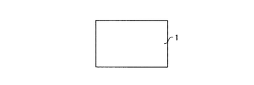
図1〜図3は、本発明にかかる半導体装置の製造方法の一例を工程順に示した要部断面図である。まず、半導体基板1として、例えば5インチ径のN-FZウェハーを用意する(図1)。例えば1200Vクラスの場合、半導体基板1の比抵抗は40〜70Ωcmである。この半導体基板1を第1半導体層として用い、標準的なダイオードのプロセス工程によって、半導体基板1の一方の主面に第2半導体層となるPアノード層2と、図示しないガードリングエッジ構造を形成する。さらに、Pアノード層2にオーミック接触する第1電極としてアノード電極3を形成する。図中200は、この状態における不純物濃度のプロファイルを示している。
1 to 3 are cross-sectional views of relevant parts showing an example of a method of manufacturing a semiconductor device according to the present invention in the order of steps. First, for example, an N − FZ wafer having a diameter of 5 inches is prepared as the semiconductor substrate 1 (FIG. 1). For example, in the case of the 1200 V class, the specific resistance of the
続いて、半導体基板1に電子線等のイオン化した荷電粒子を照射して半導体基板1の中に結晶欠陥を導入し、熱処理を行う。次いで、ウェハー(半導体基板1)の他方の主面に対して研削やウエットエッチングなどを行い、ウェハーを所定の厚さにする。例えば1200Vクラスの場合には、ウェハーの厚さを100〜160μmにするのが一般的である。その後、半導体基板1の研削等により露出した面(以下、研削による露出面とする)に対して不純物のイオン注入を行い、半導体基板1の中に不純物を導入する。
Subsequently, the
さらに、研削による露出面にYAG第2高調波レーザ等のレーザ光をダブルパルス法にて照射する。ダブルパルス法とは、レーザ光の照射エリアごとに、複数のレーザ照射装置から所定の遅延時間だけ照射タイミングをずらして複数のパルスレーザを連続的に照射する方法である。ダブルパルス法については、本発明者らが先に出願した特願2004−036547号の明細書(例えば、段落番号0030〜0032、0037)を参照されたい。 Further, a laser beam such as a YAG second harmonic laser is irradiated on the exposed surface by grinding by a double pulse method. The double pulse method is a method of continuously irradiating a plurality of pulse lasers by shifting the irradiation timing by a predetermined delay time from a plurality of laser irradiation apparatuses for each laser light irradiation area. Regarding the double pulse method, refer to the specification (for example, paragraph numbers 0030 to 0032, 0037) of Japanese Patent Application No. 2004-036547 filed earlier by the present inventors.
本実施の形態では、ダブルパルス法によりレーザ光を照射する際のエネルギー密度は、レーザ光の照射エリアごとに、合計で1J/cm2以上4J/cm2以下である。このレーザ照射によって、半導体基板1の中の不純物が電気的に活性化して第3半導体層となるN+カソード層4ができる。
In this embodiment mode, the energy density at the time of laser beam irradiation by the double pulse method is 1 J / cm 2 or more and 4 J / cm 2 or less in total for each laser beam irradiation area. By this laser irradiation, impurities in the
同時に、荷電粒子の照射により半導体基板1の中に導入された結晶欠陥のうち、レーザ光の照射面、すなわち研削による露出面から、研削後の全体の厚さの5%に相当する深さ以上30%に相当する深さ以下の範囲の任意の深さまでの領域の結晶欠陥が回復する。例えば、研削後の全体の厚さが140μmである場合には、レーザ光の照射面から、10μm以上40μm以下の範囲の任意の深さまでの領域で結晶欠陥が回復する。その後、研削による露出面にチタン(Ti)、ニッケル(Ni)および金(Au)をこの順で積層させて第2電極となるカソード電極5を形成する(図3)。図中300は、この状態における不純物濃度のプロファイルを示している。
At the same time, of crystal defects introduced into the
次に、上述した製造方法により作製されたダイオードの特性について説明する。図4は、上述した製造方法により作製されたダイオードの構成および特性を説明するための図である。図4は、ダイオードの要部断面を表している。また、アノード電極3からの距離とネットドーピング濃度との関係の特性図410と、アノード電極3からの距離とライフタイム分布との関係の特性図420を示した。特性図410,420の横軸、すなわちアノード電極3からの距離は、上部の断面図に対応している。
Next, characteristics of the diode manufactured by the manufacturing method described above will be described. FIG. 4 is a diagram for explaining the configuration and characteristics of a diode manufactured by the manufacturing method described above. FIG. 4 shows a cross section of the main part of the diode. Further, a characteristic diagram 410 showing the relationship between the distance from the
ここでは、一例として、1200Vクラスの耐圧で、150Aの定格電流となるように、チップサイズを10mm×10mmとした。また、半導体基板1の比抵抗は60Ωcmであり、半導体基板1のリン濃度は8.0×10¹³atoms/ccであった。また、Pアノード層2の濃度を5×1016atoms/ccとし、その深さを3μmとした。アノード電極は、AlSi1%で形成した。
Here, as an example, the chip size is set to 10 mm × 10 mm so that the rated current is 150 A with a breakdown voltage of 1200 V class. The specific resistance of the
また、電子線を加速電圧4.8MeVで、線量を100kGyで照射することによって結晶欠陥を導入した。電子線照射後、350℃で1時間程度の熱処理を行った。さらに、研削やウエットエッチングなどによってウェハーの厚さを140μmにした。また、N+カソード層4を形成するために、加速電圧50keVで、ドーズ量1×10¹⁹atoms/cm2のリンをイオン注入した。さらに、YAG第2高調波レーザを照射する際の、エネルギー密度を合計で3J/cm2とし、ダブルパルスの遅延時間を300nsとした。 In addition, crystal defects were introduced by irradiating an electron beam at an acceleration voltage of 4.8 MeV and a dose of 100 kGy. After the electron beam irradiation, heat treatment was performed at 350 ° C. for about 1 hour. Further, the thickness of the wafer was 140 μm by grinding or wet etching. Further, in order to form the N + cathode layer 4, phosphorus with a dose of 1 × 10 19 atoms / cm 2 was ion-implanted at an acceleration voltage of 50 keV. Further, the energy density when irradiating the YAG second harmonic laser was 3 J / cm 2 in total, and the delay time of the double pulse was 300 ns.
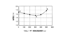
本発明者らは、YAGレーザ照射時のダブルパルスの照射遅延時間を種々変更してダイオードを作製し、得られたダイオードの電気的特性を調べた結果、照射遅延時間によって順電圧に明確な差が生じることを見出した。図5は、YAGレーザ照射時のダブルパルスの照射遅延時間と、図4に示すダイオードの150Aにおける順電圧(室温)との関係を示す図である。図5から明らかなように、照射遅延時間が0ns、100ns、200ns、300ns、400nsおよび500nsのときの順電圧は、それぞれ約1.7V、約1.64V、約1.56V、約1.52V、約1.56Vおよび約1.76Vである。 The inventors of the present invention manufactured diodes by variously changing the irradiation delay time of the double pulse at the time of YAG laser irradiation, and investigated the electrical characteristics of the obtained diode. As a result, a clear difference in forward voltage was found depending on the irradiation delay time. Has been found to occur. FIG. 5 is a diagram showing the relationship between the irradiation delay time of the double pulse during YAG laser irradiation and the forward voltage (room temperature) at 150A of the diode shown in FIG. As is clear from FIG. 5, the forward voltages when the irradiation delay times are 0 ns, 100 ns, 200 ns, 300 ns, 400 ns and 500 ns are about 1.7 V, about 1.64 V, about 1.56 V and about 1.52 V, respectively. , About 1.56V and about 1.76V.
このように順電圧に差が生じる理由は、以下の通りである。すなわち、YAGレーザを照射する前の状態では、周知のように、電子線照射による結晶欠陥はウェハーに一様に分布している。本実施の形態のように、ウェハーを研削および研磨し、リンをイオン注入した後に、上述した条件でYAGレーザを照射することによって、その照射面から約2.6μmの深さまでの領域では1414℃以上の高温となり、シリコンが溶融する。 The reason for the difference in forward voltage is as follows. That is, in a state before YAG laser irradiation, as is well known, crystal defects due to electron beam irradiation are uniformly distributed on the wafer. As in this embodiment, after grinding and polishing the wafer and ion-implanting phosphorus, the YAG laser is irradiated under the above-described conditions, so that the region from the irradiated surface to a depth of about 2.6 μm is 1414 ° C. It becomes the above high temperature and silicon melts.
YAGレーザの照射が終わると、100nsのオーダーで急速に温度が減少する。レーザの照射終了から1μs経過した時点で、その照射面から30μmの深さの位置では約500℃になる。すなわち、レーザの照射面から30μmの深さまでの領域の温度は500℃以上であり、容易に電子線照射による結晶欠陥が回復する。従って、この領域のライフタイムは、電子線照射前の値(約30μs)まで回復する。
When irradiation with the YAG laser is finished, the temperature rapidly decreases on the order of 100 ns. When 1 μs has elapsed from the end of laser irradiation, the temperature is about 500 ° C. at a
次に、デバイスシミュレーションにより、ライフタイム分布を仮定し、そのときの順電圧を計算した。図6は、仮定したライフタイム分布を示す図であり、横軸をアノード電極3からの距離とし、縦軸をライフタイムとしている。また、N+カソード層4とカソード電極5との界面を140μmの位置にしている。
Next, a lifetime distribution was assumed by device simulation, and the forward voltage at that time was calculated. FIG. 6 is a diagram showing the assumed lifetime distribution, in which the horizontal axis represents the distance from the
ここでは、電子線照射を想定した従来の一様なライフタイムを0.35μsと仮定している。そして、N+カソード層4とカソード電極5との界面から20μm(図6の7%回復の場合)、40μm(図6の21%回復の場合)、60μm、80μm、100μm、120μmおよび140μmまでの領域で結晶欠陥が回復してライフタイムが15μsになり、それぞれ、それよりも手前の領域(アノード電極3寄りの領域)のライフタイムを0.35μsと仮定している。
Here, it is assumed that the conventional uniform lifetime assuming electron beam irradiation is 0.35 μs. Then, from the interface between the N + cathode layer 4 and the
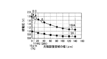
図7は、図6に示すようにライフタイム分布を仮定したときの、結晶欠陥の回復領域の幅と150Aおよび5Aの電流が流れるときの順電圧との関係を示す図である。なお、結晶欠陥の回復領域の幅とは、図6に示すライフタイム分布においてライフタイムが15μsとなっている領域の幅のことである。
FIG. 7 is a diagram showing the relationship between the width of the crystal defect recovery region and the forward voltage when the
図7から、150Aおよび5Aのいずれにおいても、結晶欠陥の回復領域の幅が伸びるほど順電圧が低くなることがわかる。150Aの場合、結晶欠陥の回復領域の幅が20μm(ウェハーの最終厚さの全体に対して約14%)のときの順電圧は、結晶欠陥の回復領域の幅が0μmのときの順電圧、すなわち結晶欠陥の回復領域がない場合の順電圧よりも約0.2V低くなる。 From FIG. 7, it can be seen that in both 150A and 5A, the forward voltage decreases as the width of the crystal defect recovery region increases. In the case of 150 A, the forward voltage when the width of the crystal defect recovery region is 20 μm (about 14% with respect to the entire final thickness of the wafer) is the forward voltage when the width of the crystal defect recovery region is 0 μm, That is, it is about 0.2 V lower than the forward voltage when there is no crystal defect recovery region.
また、図5の実測値から、150Aの場合、最も結晶欠陥が回復している、すなわち最も順電圧が低いのは、YAGレーザ照射時のダブルパルスの照射遅延時間が300nsで、順電圧が約1.52Vの場合(図5のA)であることがわかる。150Aの場合、図7にAで示すように、約1.52Vの順電圧に対応する結晶欠陥の回復領域の幅は、約30μmであることがわかる。つまり、ウェハーの最終厚さの全体に対して約21%の領域で結晶欠陥が回復したときに最も順電圧が低くなることがわかる。 Further, from the actual measurement value of FIG. 5, in the case of 150 A, the crystal defects are recovered most, that is, the lowest forward voltage is that the double pulse irradiation delay time during YAG laser irradiation is 300 ns, and the forward voltage is about It can be seen that this is the case of 1.52 V (A in FIG. 5). In the case of 150 A, as shown by A in FIG. 7, it can be seen that the width of the crystal defect recovery region corresponding to the forward voltage of about 1.52 V is about 30 μm. That is, it can be seen that the forward voltage is lowest when the crystal defects are recovered in a region of about 21% of the entire final thickness of the wafer.
換言すれば、順電圧を最も低くするには、ウェハーの最終厚さの全体に対して約21%の領域で結晶欠陥を回復させればよいことになる。また、図7に示すように、YAGレーザ照射時のダブルパルスの照射遅延時間が500nsで、順電圧が約1.76Vの場合(図5のB)の結晶欠陥の回復領域の幅は、約5μm(ウェハーの最終厚さの全体に対して約3%)である。さらに、YAGレーザ照射時のダブルパルスの照射遅延時間が0nsで、順電圧が約1.7Vの場合(図5のC)の結晶欠陥の回復領域の幅は、約10μm(ウェハーの最終厚さの全体に対して約7%)である。 In other words, in order to make the forward voltage the lowest, it is only necessary to recover crystal defects in a region of about 21% of the entire final thickness of the wafer. As shown in FIG. 7, the width of the crystal defect recovery region when the double pulse irradiation delay time during YAG laser irradiation is 500 ns and the forward voltage is about 1.76 V (FIG. 5B) is about 5 μm (about 3% of the total final thickness of the wafer). Further, when the irradiation delay time of the double pulse at the time of YAG laser irradiation is 0 ns and the forward voltage is about 1.7 V (C in FIG. 5), the width of the crystal defect recovery region is about 10 μm (final thickness of the wafer). About 7%).
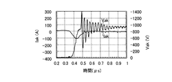
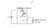
図8、図9および図10は、それぞれ図11に示す単相チョッパー回路10における図5のA、BおよびCで示すダイオードの室温での逆回復波形を示す図である。これらの図において、Iakはアノード電流であり、Vakはアノード・カソード間の電圧である。単相チョッパー回路10では、逆回復順電流が15Aで定格電流の1/10であり、DCバス電圧が900Vであり、負荷インダクタンスLmが1mHである。また、スイッチングIGBTは、標準的な1200V/150AのFS(フィールドストップ型)−IGBTであり、そのゲート抵抗は、オン側で0Ωであり、オフ側で33Ωである。主回路の回路浮遊インダクタンスLsは200nHである。
8, FIG. 9, and FIG. 10 are diagrams showing reverse recovery waveforms at room temperature of the diodes indicated by A, B, and C in FIG. 5 in the single-
図8〜図10から明らかなように、最も結晶欠陥を回復させたAのダイオードが、発振がなくソフトリカバリーであることがわかる。それに対して、Cのダイオードは、丁度発振を開始する条件にあり、また、Bのダイオードは明らかに発振しており、そのピーク電圧がAおよびCの両ダイオードよりもはるかに高いことがわかる。従って、ソフトリカバリーとするには、結晶欠陥の回復領域を増やせばよいことがわかる。ただし、ウェハー全体にわたって結晶欠陥を回復させてしまうと全く意味をなさなくなる。 As is apparent from FIGS. 8 to 10, it can be seen that the diode A that has recovered the most crystal defects is soft recovery without oscillation. On the other hand, the C diode is in a condition to just start oscillation, and the B diode is clearly oscillating, and it can be seen that its peak voltage is much higher than both the A and C diodes. Therefore, it can be seen that the soft recovery can be achieved by increasing the recovery area of crystal defects. However, if crystal defects are recovered over the entire wafer, it makes no sense.
以上の結果より、N+カソード層4とカソード電極5との界面から、薄板化した後のウェハー全体の厚さの5%以上に相当する深さまでの領域で結晶欠陥を回復させれば、ソフトリカバリー効果が得られることは明白である。また、結晶欠陥を回復させる領域の、N+カソード層4とカソード電極5との界面からの深さを、薄板化した後のウェハー全体の厚さの20〜30%にすることによって、十分なソフトリカバリー効果が得られる。
From the above results, if crystal defects are recovered in a region from the interface between the N + cathode layer 4 and the
なお、N+カソード層4とカソード電極5との界面から、薄板化した後のウェハー全体の厚さの30%(本実施の形態では、約40μm)を超える深さまでの領域で結晶欠陥を回復させようとすると、YAGレーザの照射エネルギー密度をおよそ4J/cm2以上にする必要がある。この場合には、レーザ照射面の温度がシリコンの沸点(3267℃)を超えてしまうため、アブレーションが生じ、レーザ照射面が荒れてしまう。従って、結晶欠陥の回復領域は、レーザ照射面から、薄板化した後のウェハー全体の厚さの30%に相当する深さまでの範囲であるのが望ましい。
It should be noted that crystal defects are recovered in a region extending from the interface between the N + cathode layer 4 and the
N+カソード層4を形成するために研削による露出面から半導体基板1の中に注入したリンを活性化させるためだけであれば、1J/cm2以下、例えば500mJ/cm2の照射エネルギー密度で、0nsの照射遅延時間、すなわち遅延なしでYAGレーザのパルスを照射すれば、十分にコンタクト抵抗の低いN+カソード層4を形成することができる。また、YAGレーザに限らず、エネルギー密度の低いエキシマレーザなどを用いても同様である。しかし、本実施の形態のように電子線等の軽い荷電粒子の照射によって結晶欠陥を生成し、かつソフトリカバリーとするためには、上述したダブルパルス法でYAGレーザを照射して、ソフトリカバリーに必要な結晶欠陥の回復分布、すなわちライフタイム分布を得る必要がある。
If it is only to activate phosphorus implanted into the
1200V以外の耐圧クラス、例えば600Vクラスのダイオードについても同様である。600Vクラスについては、半導体基板の比抵抗を15〜30Ωcm、例えば20Ωcmとし、研削および研磨後の最終的なウェハー厚さを50〜70μm、例えば60μmとする。そして、例えば、電子線照射の照射線量を300kGyとし、YAGレーザの照射エネルギー密度を2.8J/cm2とし、照射遅延時間を300nsにすれば、順方向電流の電流密度が400A/cm2のときに順電圧は1.3Vとなる。 The same applies to a withstand voltage class other than 1200 V, for example, a 600 V class diode. For the 600V class, the specific resistance of the semiconductor substrate is 15-30 Ωcm, for example 20 Ωcm, and the final wafer thickness after grinding and polishing is 50-70 μm, for example 60 μm. For example, if the irradiation dose of electron beam irradiation is 300 kGy, the irradiation energy density of the YAG laser is 2.8 J / cm 2 , and the irradiation delay time is 300 ns, the current density of the forward current is 400 A / cm 2 . Sometimes the forward voltage is 1.3V.
同じ条件で、照射遅延時間を500nsにすると、順電圧は1.6Vとなり、図5と同様の特性が得られる。DCバス電圧500V、電流密度400A/cm2からの逆回復波形(室温)は、照射遅延時間が300nsのダイオードでは発振がなく、照射遅延時間が500nsのダイオードでは発振する。 Under the same conditions, when the irradiation delay time is 500 ns, the forward voltage becomes 1.6 V, and the same characteristics as in FIG. 5 can be obtained. A reverse recovery waveform (room temperature) from a DC bus voltage of 500 V and a current density of 400 A / cm 2 does not oscillate in a diode with an irradiation delay time of 300 ns, and oscillates in a diode with an irradiation delay time of 500 ns.
また、本発明は、ダイオードに限らず、通常のIGBTや逆阻止IGBTに適用することもできる。本発明を適用したIGBT等では、低損失で、かつ発振を抑えたターンオフを実現できる。特に、逆阻止IGBTを作製する際には、FZバルクウェハーを用い、そのおもて面にゲート構造やエミッタ構造やエッジ構造を作製し、電子線を100kGy以下で照射した後に、ウェハー全体の最終的な厚さが100μm前後になるようにウェハーの裏面を研削および研磨し、研削による露出面に対してボロンのイオン注入とレーザ照射によるボロンの活性化工程がある。 In addition, the present invention is not limited to a diode, and can also be applied to a normal IGBT or a reverse blocking IGBT. An IGBT or the like to which the present invention is applied can realize turn-off with low loss and suppressed oscillation. In particular, when fabricating a reverse blocking IGBT, an FZ bulk wafer is used, a gate structure, an emitter structure, and an edge structure are fabricated on the front surface, and an electron beam is irradiated at 100 kGy or less, and then the final wafer is finished. There is a step of grinding and polishing the back surface of the wafer so that the typical thickness is about 100 μm, and boron activation for the exposed surface by grinding and boron ion implantation.
一方、ターンオフ時には、ダイオードの逆回復と同様に表側から空乏層が広がり、キャリアが消滅していくが、ダイオードの場合と同様に、キャリアの急激な消滅を抑えることができるので、発振のないスムーズなターンオフが可能となる。従って、低損失でソフトリカバリーなダイオードや、発振のないスムーズなターンオフが可能なIGBTを作製することができる。また、そのような特性を有するIGBTモジュールを用いたPWMインバータ等の電力変換装置において、過電圧破壊やEMIノイズの発生を抑えることができる。 On the other hand, at the turn-off time, the depletion layer spreads from the front side and the carriers disappear as in the reverse recovery of the diode. However, as in the case of the diode, since the rapid disappearance of the carrier can be suppressed, there is no oscillation. Turn-off is possible. Therefore, a low-loss and soft-recovery diode and an IGBT that can be smoothly turned off without oscillation can be manufactured. Moreover, in a power converter such as a PWM inverter using an IGBT module having such characteristics, overvoltage breakdown and generation of EMI noise can be suppressed.
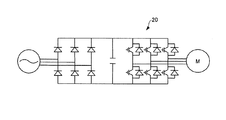
図12および図13は、実施の形態のダイオードやFS−IGBTの適用例を示す図である。図12に示すAC−AC用インバータ−コンバーター20は、効率良く誘導電動機やサーボモータ等を制御することが可能で、産業や電鉄などで広く用いられる。図13に示す力率改善回路(PFC回路)30は、AC−AC変換の入力電流を正弦波状に制御して波形改善をはかる回路であり、スイッチング電源用に用いられる。
12 and 13 are diagrams illustrating application examples of the diode and the FS-IGBT according to the embodiment. An AC-AC inverter-
実施の形態によれば、逆回復時間および損失が従来よりも大幅に低減し、かつソフトリカバリー特性が向上したダイオードを実現できる。また、電気的損失および放射電磁ノイズの低い、環境問題を考慮したIGBTモジュールやIPMを実現できる。 According to the embodiment, it is possible to realize a diode in which the reverse recovery time and loss are significantly reduced as compared with the conventional diode and the soft recovery characteristic is improved. In addition, an IGBT module or IPM that takes into consideration environmental problems with low electrical loss and radiated electromagnetic noise can be realized.
以上において本発明は、上述した実施の形態に限らず、種々変更可能である。例えば、実施の形態中に記載した寸法や濃度などは一例であり、本発明はそれらの値に限定されるものではない。また、各実施の形態では第1導電型をN型とし、第2導電型をP型としたが、本発明は第1導電型をP型とし、第2導電型をN型としても同様に成り立つ。 As described above, the present invention is not limited to the above-described embodiment, and various modifications can be made. For example, the dimensions and concentrations described in the embodiments are examples, and the present invention is not limited to these values. In each embodiment, the first conductivity type is N-type and the second conductivity type is P-type. However, in the present invention, the first conductivity type is P-type and the second conductivity type is N-type. It holds.
以上のように、本発明にかかる半導体装置の製造方法は、電力用半導体装置に有用であり、特に、高速かつ低損失であるとともに、ソフトリカバリー特性を備えたダイオードまたはIGBTに適している。 As described above, the method for manufacturing a semiconductor device according to the present invention is useful for a power semiconductor device, and is particularly suitable for a diode or IGBT having high recovery speed and low loss and soft recovery characteristics.
1 第1半導体層(半導体基板)
2 第2半導体層(Pアノード層)
3 第1電極(アノード電極)
4 第3半導体層(N+カソード層)
5 第2電極(カソード電極)
1 First semiconductor layer (semiconductor substrate)
2 Second semiconductor layer (P anode layer)
3 First electrode (anode electrode)
4 Third semiconductor layer (N + cathode layer)
5 Second electrode (cathode electrode)
Claims (9)
第1導電型半導体基板の一方または他方の主面に荷電粒子を照射して前記半導体基板中に結晶欠陥を導入する工程と、
前記第1半導体層のキャリアのライフタイムを、前記荷電粒子を照射する前の値よりも低い値となるように熱処理する熱処理工程と、
結晶欠陥が導入された半導体基板の前記他方の主面を研削する工程と、
研削により露出した面から前記半導体基板中に第1導電型または第2導電型の不純物をイオン注入法により導入する工程と、
研削により露出した面にレーザ光を照射して、前記半導体基板中に導入された不純物を電気的に活性化させるとともに、前記半導体基板中に導入された結晶欠陥のうち、レーザ光の照射面から所定の深さまでの領域のキャリアのライフタイムが前記熱処理工程後のキャリアのライフタイムよりも高い値となるように結晶欠陥を回復させる回復工程と、
を含み、
レーザ光の照射により結晶欠陥を回復させる領域を、レーザ光の照射面から、研削後の全体の厚さの5%に相当する深さ以上30%に相当する深さ以下の範囲の任意の深さまでとすることを特徴とする半導体装置の製造方法。 A first semiconductor layer of a first conductivity type and a second semiconductor of a second conductivity type having a higher concentration than the first semiconductor layer and in contact with the first semiconductor layer on one main surface side of the first semiconductor layer A layer, a first electrode electrically connected to the second semiconductor layer, and a higher concentration than the first semiconductor layer and in contact with the first semiconductor layer on the other main surface side of the first semiconductor layer In manufacturing a semiconductor device including a third semiconductor layer of a first conductivity type and a second electrode electrically connected to the third semiconductor layer,
Irradiating one or the other main surface of the first conductivity type semiconductor substrate with charged particles to introduce crystal defects in the semiconductor substrate;
A heat treatment step of the carrier lifetime of the first semiconductor layer, a heat treatment such that the value smaller than that prior to irradiation with the charged particle,
Grinding the other principal surface of the semiconductor substrate into which crystal defects have been introduced;
Introducing an impurity of a first conductivity type or a second conductivity type into the semiconductor substrate from a surface exposed by grinding by an ion implantation method;
The surface exposed by grinding is irradiated with laser light to electrically activate impurities introduced into the semiconductor substrate, and among crystal defects introduced into the semiconductor substrate, from the laser light irradiation surface a recovery step of the carrier lifetime in the region up to a predetermined depth Ru restored the crystal defects so that the value higher than the lifetime of carriers after the heat treatment step,
Only including,
A region where crystal defects are recovered by laser light irradiation is an arbitrary depth within a range from a depth corresponding to 5% of a total thickness after grinding to a depth corresponding to 30% from the laser light irradiation surface. the method of manufacturing a semiconductor device which is characterized in that up is.
Priority Applications (2)
| Application Number | Priority Date | Filing Date | Title |
|---|---|---|---|
| JP2005246037A JP5087828B2 (en) | 2005-08-26 | 2005-08-26 | Manufacturing method of semiconductor device |
| US11/464,489 US7517777B2 (en) | 2005-08-26 | 2006-08-14 | Method of manufacturing semiconductor device and semiconductor device formed by the method |
Applications Claiming Priority (1)
| Application Number | Priority Date | Filing Date | Title |
|---|---|---|---|
| JP2005246037A JP5087828B2 (en) | 2005-08-26 | 2005-08-26 | Manufacturing method of semiconductor device |
Related Child Applications (1)
| Application Number | Title | Priority Date | Filing Date |
|---|---|---|---|
| JP2012127604A Division JP5672269B2 (en) | 2012-06-04 | 2012-06-04 | Manufacturing method of semiconductor device |
Publications (2)
| Publication Number | Publication Date |
|---|---|
| JP2007059801A JP2007059801A (en) | 2007-03-08 |
| JP5087828B2 true JP5087828B2 (en) | 2012-12-05 |
Family
ID=37804808
Family Applications (1)
| Application Number | Title | Priority Date | Filing Date |
|---|---|---|---|
| JP2005246037A Expired - Lifetime JP5087828B2 (en) | 2005-08-26 | 2005-08-26 | Manufacturing method of semiconductor device |
Country Status (2)
| Country | Link |
|---|---|
| US (1) | US7517777B2 (en) |
| JP (1) | JP5087828B2 (en) |
Families Citing this family (16)
| Publication number | Priority date | Publication date | Assignee | Title |
|---|---|---|---|---|
| JP5043445B2 (en) * | 2007-01-16 | 2012-10-10 | 三菱電機株式会社 | Manufacturing method of semiconductor device |
| JP5309360B2 (en) * | 2008-07-31 | 2013-10-09 | 三菱電機株式会社 | Semiconductor device and manufacturing method thereof |
| JP5307093B2 (en) * | 2010-08-23 | 2013-10-02 | 株式会社日本製鋼所 | Manufacturing method of semiconductor device |
| WO2014030457A1 (en) * | 2012-08-22 | 2014-02-27 | 富士電機株式会社 | Semiconductor device and method for manufacturing semiconductor device |
| JP5610493B2 (en) * | 2012-10-03 | 2014-10-22 | 株式会社日本製鋼所 | Semiconductor device manufacturing method and manufacturing apparatus |
| CN103855198B (en) * | 2012-11-29 | 2017-04-12 | 上海联星电子有限公司 | A reverse conduction type IGBT device and its forming method |
| CN103208532B (en) * | 2013-02-28 | 2015-06-10 | 溧阳市宏达电机有限公司 | Fin type positive-intrinsic-negative (PIN) diode |
| JP6291981B2 (en) * | 2013-04-08 | 2018-03-14 | 富士電機株式会社 | Manufacturing method of semiconductor device |
| JP6221436B2 (en) | 2013-07-10 | 2017-11-01 | 富士電機株式会社 | Superjunction MOSFET, manufacturing method thereof, and composite semiconductor device in which diodes are connected in parallel |
| CN105122458B (en) | 2013-09-18 | 2018-02-02 | 富士电机株式会社 | Semiconductor device and its manufacture method |
| CN105814694B (en) | 2014-10-03 | 2019-03-08 | 富士电机株式会社 | Semiconductor device and method of manufacturing the same |
| JP6344483B2 (en) | 2014-11-17 | 2018-06-20 | 富士電機株式会社 | Semiconductor device and manufacturing method of semiconductor device |
| CN107112370B (en) * | 2015-06-30 | 2020-08-28 | 富士电机株式会社 | Semiconductor device and method of manufacturing the same |
| DE102018000395A1 (en) * | 2018-01-18 | 2019-07-18 | 3-5 Power Electronics GmbH | Stacked III-V semiconductor diode |
| US11769827B2 (en) | 2020-12-02 | 2023-09-26 | Wolfspeed, Inc. | Power transistor with soft recovery body diode |
| US11990543B2 (en) | 2020-12-02 | 2024-05-21 | Wolfspeed, Inc. | Power transistor with soft recovery body diode |
Family Cites Families (24)
| Publication number | Priority date | Publication date | Assignee | Title |
|---|---|---|---|---|
| JPS5817678A (en) * | 1981-07-24 | 1983-02-01 | Toshiba Corp | Manufacture of semiconductor device |
| JPH0562924A (en) | 1991-09-04 | 1993-03-12 | Sony Corp | Laser annealing equipment |
| JP3105488B2 (en) | 1992-10-21 | 2000-10-30 | 株式会社半導体エネルギー研究所 | Laser treatment method |
| US6090646A (en) | 1993-05-26 | 2000-07-18 | Semiconductor Energy Laboratory Co., Ltd. | Method for producing semiconductor device |
| JPH07226405A (en) * | 1994-12-19 | 1995-08-22 | Meidensha Corp | Method for manufacturing semiconductor device |
| US5569624A (en) | 1995-06-05 | 1996-10-29 | Regents Of The University Of California | Method for shallow junction formation |
| US6534380B1 (en) | 1997-07-18 | 2003-03-18 | Denso Corporation | Semiconductor substrate and method of manufacturing the same |
| JP3706026B2 (en) | 1998-07-17 | 2005-10-12 | インフィネオン テクノロジース アクチエンゲゼルシャフト | Power semiconductor elements for high reverse voltage |
| US6393042B1 (en) | 1999-03-08 | 2002-05-21 | Semiconductor Energy Laboratory Co., Ltd. | Beam homogenizer and laser irradiation apparatus |
| JP2000349042A (en) | 1999-06-03 | 2000-12-15 | Toshiba Corp | Semiconductor device manufacturing method and manufacturing apparatus |
| JP4862207B2 (en) * | 1999-11-26 | 2012-01-25 | 富士電機株式会社 | Manufacturing method of semiconductor device |
| DE10055446B4 (en) * | 1999-11-26 | 2012-08-23 | Fuji Electric Co., Ltd. | Semiconductor component and method for its production |
| JP4514861B2 (en) | 1999-11-29 | 2010-07-28 | 株式会社半導体エネルギー研究所 | Laser irradiation apparatus, laser irradiation method, and manufacturing method of semiconductor device |
| JP2001177114A (en) | 1999-12-17 | 2001-06-29 | Fuji Electric Co Ltd | Semiconductor device |
| JP2001185504A (en) | 1999-12-22 | 2001-07-06 | Sanyo Electric Co Ltd | Laser anneal method and device |
| JP4967205B2 (en) | 2001-08-09 | 2012-07-04 | 富士電機株式会社 | Manufacturing method of semiconductor device |
| JP2003109912A (en) | 2001-10-01 | 2003-04-11 | Matsushita Electric Ind Co Ltd | Laser annealing equipment |
| JP4539011B2 (en) | 2002-02-20 | 2010-09-08 | 富士電機システムズ株式会社 | Semiconductor device |
| JP4364674B2 (en) | 2003-02-28 | 2009-11-18 | 株式会社半導体エネルギー研究所 | Method for manufacturing semiconductor device |
| DE102004017723B4 (en) * | 2003-04-10 | 2011-12-08 | Fuji Electric Co., Ltd | Backward blocking semiconductor device and method of making the same |
| JP4590880B2 (en) * | 2003-06-24 | 2010-12-01 | 富士電機システムズ株式会社 | Manufacturing method of semiconductor device |
| DE102004030268B4 (en) * | 2003-06-24 | 2013-02-21 | Fuji Electric Co., Ltd | Method for producing a semiconductor element |
| JP4096838B2 (en) * | 2003-08-20 | 2008-06-04 | 富士電機デバイステクノロジー株式会社 | Semiconductor device and manufacturing method thereof |
| JP4872190B2 (en) | 2004-06-18 | 2012-02-08 | トヨタ自動車株式会社 | Semiconductor device |
-
2005
- 2005-08-26 JP JP2005246037A patent/JP5087828B2/en not_active Expired - Lifetime
-
2006
- 2006-08-14 US US11/464,489 patent/US7517777B2/en active Active
Also Published As
| Publication number | Publication date |
|---|---|
| US7517777B2 (en) | 2009-04-14 |
| JP2007059801A (en) | 2007-03-08 |
| US20070048982A1 (en) | 2007-03-01 |
Similar Documents
| Publication | Publication Date | Title |
|---|---|---|
| JP7147891B2 (en) | semiconductor equipment | |
| US11469297B2 (en) | Semiconductor device and method for producing semiconductor device | |
| JP5374883B2 (en) | Semiconductor device and manufacturing method thereof | |
| JP5087828B2 (en) | Manufacturing method of semiconductor device | |
| CN101305470B (en) | Semiconductor device and method for manufacturing the same | |
| US8163630B2 (en) | Method of manufacturing a semiconductor device | |
| JP5396689B2 (en) | Semiconductor device and manufacturing method thereof | |
| CN106463528B (en) | Method for manufacturing silicon carbide semiconductor device | |
| US20150303268A1 (en) | Diode and power conversion device | |
| WO2013108911A1 (en) | Semiconductor device and method for producing same | |
| JP2013197306A (en) | Manufacturing method of semiconductor device | |
| JP5033335B2 (en) | Semiconductor device and inverter device using the same | |
| JP6294175B2 (en) | Semiconductor device and power conversion system using the same | |
| JP2007158320A (en) | Semiconductor device and manufacturing method thereof | |
| JP5672269B2 (en) | Manufacturing method of semiconductor device | |
| JP5162964B2 (en) | Semiconductor device and semiconductor power conversion device | |
| JP2014056976A (en) | Semiconductor device and manufacturing method of the same | |
| JP2014220516A (en) | Semiconductor device |
Legal Events
| Date | Code | Title | Description |
|---|---|---|---|
| A621 | Written request for application examination |
Free format text: JAPANESE INTERMEDIATE CODE: A621 Effective date: 20080715 |
|
| A711 | Notification of change in applicant |
Free format text: JAPANESE INTERMEDIATE CODE: A712 Effective date: 20091112 |
|
| RD03 | Notification of appointment of power of attorney |
Free format text: JAPANESE INTERMEDIATE CODE: A7423 Effective date: 20091112 |
|
| RD04 | Notification of resignation of power of attorney |
Free format text: JAPANESE INTERMEDIATE CODE: A7424 Effective date: 20091112 |
|
| A711 | Notification of change in applicant |
Free format text: JAPANESE INTERMEDIATE CODE: A712 Effective date: 20110422 |
|
| A977 | Report on retrieval |
Free format text: JAPANESE INTERMEDIATE CODE: A971007 Effective date: 20110811 |
|
| A131 | Notification of reasons for refusal |
Free format text: JAPANESE INTERMEDIATE CODE: A131 Effective date: 20110823 |
|
| A521 | Request for written amendment filed |
Free format text: JAPANESE INTERMEDIATE CODE: A523 Effective date: 20111024 |
|
| A131 | Notification of reasons for refusal |
Free format text: JAPANESE INTERMEDIATE CODE: A131 Effective date: 20120403 |
|
| A521 | Request for written amendment filed |
Free format text: JAPANESE INTERMEDIATE CODE: A523 Effective date: 20120604 |
|
| TRDD | Decision of grant or rejection written | ||
| A01 | Written decision to grant a patent or to grant a registration (utility model) |
Free format text: JAPANESE INTERMEDIATE CODE: A01 Effective date: 20120814 |
|
| A01 | Written decision to grant a patent or to grant a registration (utility model) |
Free format text: JAPANESE INTERMEDIATE CODE: A01 |
|
| A61 | First payment of annual fees (during grant procedure) |
Free format text: JAPANESE INTERMEDIATE CODE: A61 Effective date: 20120827 |
|
| FPAY | Renewal fee payment (event date is renewal date of database) |
Free format text: PAYMENT UNTIL: 20150921 Year of fee payment: 3 |
|
| R150 | Certificate of patent or registration of utility model |
Ref document number: 5087828 Country of ref document: JP Free format text: JAPANESE INTERMEDIATE CODE: R150 Free format text: JAPANESE INTERMEDIATE CODE: R150 |
|
| R250 | Receipt of annual fees |
Free format text: JAPANESE INTERMEDIATE CODE: R250 |
|
| R250 | Receipt of annual fees |
Free format text: JAPANESE INTERMEDIATE CODE: R250 |
|
| R250 | Receipt of annual fees |
Free format text: JAPANESE INTERMEDIATE CODE: R250 |
|
| R250 | Receipt of annual fees |
Free format text: JAPANESE INTERMEDIATE CODE: R250 |
|
| R250 | Receipt of annual fees |
Free format text: JAPANESE INTERMEDIATE CODE: R250 |
|
| R250 | Receipt of annual fees |
Free format text: JAPANESE INTERMEDIATE CODE: R250 |
|
| R250 | Receipt of annual fees |
Free format text: JAPANESE INTERMEDIATE CODE: R250 |
|
| R250 | Receipt of annual fees |
Free format text: JAPANESE INTERMEDIATE CODE: R250 |
|
| R250 | Receipt of annual fees |
Free format text: JAPANESE INTERMEDIATE CODE: R250 |
|
| R250 | Receipt of annual fees |
Free format text: JAPANESE INTERMEDIATE CODE: R250 |
|
| EXPY | Cancellation because of completion of term |