JP5083245B2 - Pixel drive device, light emitting device, display device, and connection unit connection method for pixel drive device - Google Patents
Pixel drive device, light emitting device, display device, and connection unit connection method for pixel drive device Download PDFInfo
- Publication number
- JP5083245B2 JP5083245B2 JP2009046147A JP2009046147A JP5083245B2 JP 5083245 B2 JP5083245 B2 JP 5083245B2 JP 2009046147 A JP2009046147 A JP 2009046147A JP 2009046147 A JP2009046147 A JP 2009046147A JP 5083245 B2 JP5083245 B2 JP 5083245B2
- Authority
- JP
- Japan
- Prior art keywords
- connection
- input
- unit
- terminals
- output
- Prior art date
- Legal status (The legal status is an assumption and is not a legal conclusion. Google has not performed a legal analysis and makes no representation as to the accuracy of the status listed.)
- Expired - Fee Related
Links
Images


Classifications
-
- G—PHYSICS
- G09—EDUCATION; CRYPTOGRAPHY; DISPLAY; ADVERTISING; SEALS
- G09G—ARRANGEMENTS OR CIRCUITS FOR CONTROL OF INDICATING DEVICES USING STATIC MEANS TO PRESENT VARIABLE INFORMATION
- G09G3/00—Control arrangements or circuits, of interest only in connection with visual indicators other than cathode-ray tubes
- G09G3/20—Control arrangements or circuits, of interest only in connection with visual indicators other than cathode-ray tubes for presentation of an assembly of a number of characters, e.g. a page, by composing the assembly by combination of individual elements arranged in a matrix no fixed position being assigned to or needed to be assigned to the individual characters or partial characters
- G09G3/22—Control arrangements or circuits, of interest only in connection with visual indicators other than cathode-ray tubes for presentation of an assembly of a number of characters, e.g. a page, by composing the assembly by combination of individual elements arranged in a matrix no fixed position being assigned to or needed to be assigned to the individual characters or partial characters using controlled light sources
- G09G3/30—Control arrangements or circuits, of interest only in connection with visual indicators other than cathode-ray tubes for presentation of an assembly of a number of characters, e.g. a page, by composing the assembly by combination of individual elements arranged in a matrix no fixed position being assigned to or needed to be assigned to the individual characters or partial characters using controlled light sources using electroluminescent panels
- G09G3/32—Control arrangements or circuits, of interest only in connection with visual indicators other than cathode-ray tubes for presentation of an assembly of a number of characters, e.g. a page, by composing the assembly by combination of individual elements arranged in a matrix no fixed position being assigned to or needed to be assigned to the individual characters or partial characters using controlled light sources using electroluminescent panels semiconductive, e.g. using light-emitting diodes [LED]
- G09G3/3208—Control arrangements or circuits, of interest only in connection with visual indicators other than cathode-ray tubes for presentation of an assembly of a number of characters, e.g. a page, by composing the assembly by combination of individual elements arranged in a matrix no fixed position being assigned to or needed to be assigned to the individual characters or partial characters using controlled light sources using electroluminescent panels semiconductive, e.g. using light-emitting diodes [LED] organic, e.g. using organic light-emitting diodes [OLED]
- G09G3/3275—Details of drivers for data electrodes
- G09G3/3291—Details of drivers for data electrodes in which the data driver supplies a variable data voltage for setting the current through, or the voltage across, the light-emitting elements
-
- G—PHYSICS
- G09—EDUCATION; CRYPTOGRAPHY; DISPLAY; ADVERTISING; SEALS
- G09G—ARRANGEMENTS OR CIRCUITS FOR CONTROL OF INDICATING DEVICES USING STATIC MEANS TO PRESENT VARIABLE INFORMATION
- G09G2310/00—Command of the display device
- G09G2310/02—Addressing, scanning or driving the display screen or processing steps related thereto
- G09G2310/0264—Details of driving circuits
- G09G2310/0297—Special arrangements with multiplexing or demultiplexing of display data in the drivers for data electrodes, in a pre-processing circuitry delivering display data to said drivers or in the matrix panel, e.g. multiplexing plural data signals to one D/A converter or demultiplexing the D/A converter output to multiple columns
-
- G—PHYSICS
- G09—EDUCATION; CRYPTOGRAPHY; DISPLAY; ADVERTISING; SEALS
- G09G—ARRANGEMENTS OR CIRCUITS FOR CONTROL OF INDICATING DEVICES USING STATIC MEANS TO PRESENT VARIABLE INFORMATION
- G09G2320/00—Control of display operating conditions
- G09G2320/02—Improving the quality of display appearance
- G09G2320/0233—Improving the luminance or brightness uniformity across the screen
-
- G—PHYSICS
- G09—EDUCATION; CRYPTOGRAPHY; DISPLAY; ADVERTISING; SEALS
- G09G—ARRANGEMENTS OR CIRCUITS FOR CONTROL OF INDICATING DEVICES USING STATIC MEANS TO PRESENT VARIABLE INFORMATION
- G09G2320/00—Control of display operating conditions
- G09G2320/02—Improving the quality of display appearance
- G09G2320/0285—Improving the quality of display appearance using tables for spatial correction of display data
-
- G—PHYSICS
- G09—EDUCATION; CRYPTOGRAPHY; DISPLAY; ADVERTISING; SEALS
- G09G—ARRANGEMENTS OR CIRCUITS FOR CONTROL OF INDICATING DEVICES USING STATIC MEANS TO PRESENT VARIABLE INFORMATION
- G09G2320/00—Control of display operating conditions
- G09G2320/02—Improving the quality of display appearance
- G09G2320/029—Improving the quality of display appearance by monitoring one or more pixels in the display panel, e.g. by monitoring a fixed reference pixel
- G09G2320/0295—Improving the quality of display appearance by monitoring one or more pixels in the display panel, e.g. by monitoring a fixed reference pixel by monitoring each display pixel
-
- G—PHYSICS
- G09—EDUCATION; CRYPTOGRAPHY; DISPLAY; ADVERTISING; SEALS
- G09G—ARRANGEMENTS OR CIRCUITS FOR CONTROL OF INDICATING DEVICES USING STATIC MEANS TO PRESENT VARIABLE INFORMATION
- G09G2320/00—Control of display operating conditions
- G09G2320/04—Maintaining the quality of display appearance
- G09G2320/043—Preventing or counteracting the effects of ageing
Landscapes
- Engineering & Computer Science (AREA)
- Physics & Mathematics (AREA)
- Computer Hardware Design (AREA)
- General Physics & Mathematics (AREA)
- Theoretical Computer Science (AREA)
- Control Of Indicators Other Than Cathode Ray Tubes (AREA)
- Control Of El Displays (AREA)
- Electroluminescent Light Sources (AREA)
- Devices For Indicating Variable Information By Combining Individual Elements (AREA)
Description
本発明は、画素アレイを駆動する画素駆動装置、これを備える発光装置、表示装置及び画素駆動装置の接続ユニット接続方法に関するものである。 The present invention relates to a pixel driving device that drives a pixel array, a light emitting device including the pixel driving device, a display device, and a connection unit connection method for the pixel driving device.
有機エレクトロルミネッセンス素子(有機EL素子)は、電場を加えることによって発光する蛍光性の有機化合物によって形成されたものであり、これを用いた有機発光ダイオード(Organic Light Emitting Diode:以下、OLEDと記す)素子を各画素に有してなる表示パネルを備えた表示装置は次世代ディスプレイデバイスとして注目されている。 An organic electroluminescence element (organic EL element) is formed by a fluorescent organic compound that emits light when an electric field is applied, and an organic light emitting diode (hereinafter referred to as OLED) using the organic light emitting diode. A display device including a display panel having an element in each pixel has attracted attention as a next-generation display device.
このような表示装置においては、OLED素子が1画素に対応するようにそれぞれ行列配置されることによって表示パネルが形成され、画像データに基づいて、各画素のOLED素子を発光させることによって表示パネルに画像が表示される。 In such a display device, a display panel is formed by arranging the OLED elements in a matrix so as to correspond to one pixel, and based on the image data, the OLED element of each pixel is caused to emit light, thereby causing the display panel to emit light. An image is displayed.
このOLED素子は供給される電流の電流値に応じた輝度で発光する電流駆動素子であり、アクティブマトリックス駆動方式を適用した表示パネルにおいては、各画素に、1つのOLED素子と、該OLED素子に接続されて表示データに応じた電流値の駆動電流をOLED素子に流すための駆動用トランジスタを含む複数のトランジスタを有する画素駆動回路と、を備える。 This OLED element is a current driving element that emits light with a luminance corresponding to the current value of the supplied current. In a display panel to which an active matrix driving method is applied, one OLED element and one OLED element are provided for each pixel. And a pixel driving circuit having a plurality of transistors including a driving transistor for connecting a driving current having a current value corresponding to display data to the OLED element.
このような表示パネルの駆動方法としては、例えば、表示データに応じた電圧値を有する電圧信号からなる駆動信号を駆動用トランジスタのゲート・ソース電極間に印加し、これをゲート・ソース電極間の容量成分に保持し、保持した電圧成分に応じた電流値の駆動電流を駆動用トランジスタのドレイン・ソース電極間に流して、これをOLED素子に供給するように構成される。 As a method for driving such a display panel, for example, a drive signal composed of a voltage signal having a voltage value corresponding to display data is applied between the gate and source electrodes of the drive transistor, and this is applied between the gate and source electrodes. The capacitor component is held, and a drive current having a current value corresponding to the held voltage component is caused to flow between the drain and source electrodes of the driving transistor and supplied to the OLED element.
この場合、駆動電流の電流値は駆動用トランジスタのゲート電圧に対するドレイン・ソース間電流の特性によって決まるが、各画素の駆動用トランジスタにおける電気的特性にばらつきがあると、駆動電流の電流値にもばらつきを生じる。 In this case, the current value of the drive current is determined by the characteristics of the drain-source current with respect to the gate voltage of the drive transistor, but if the electrical characteristics of the drive transistor of each pixel vary, the current value of the drive current also increases. Variation occurs.
また、各画素の駆動用トランジスタの特性が駆動履歴等によって変化(劣化)した場合には、駆動電流の電流値も変動する。このような駆動電流の電流値のばらつきや変動はそのまま画質の低下につながる。 Further, when the characteristics of the driving transistor of each pixel change (deteriorate) due to the driving history or the like, the current value of the driving current also varies. Such variations and fluctuations in the current value of the drive current directly lead to a decrease in image quality.
そこで、画質の向上を図るため、駆動時に各画素の駆動用トランジスタのゲート・ソース間電圧を閾値電圧Vthに設定したうえで駆動信号を印加することによって、閾値電圧Vthのばらつきや変動の影響を抑えるようにしたものがある(例えば、特許文献1参照)。 Therefore, in order to improve the image quality, the drive signal is applied after setting the gate-source voltage of the drive transistor of each pixel to the threshold voltage Vth during driving, so that the influence of variations and fluctuations in the threshold voltage Vth is affected. Some have been made to suppress (see, for example, Patent Document 1).
しかしながら、特許文献1に記載されているような駆動方式では、駆動時に各画素の駆動用トランジスタのゲート・ソース間電圧を閾値電圧Vthに設定するための時間を必要とするが、画素数の多い高精細な表示パネルや比較的大型の表示パネルでは1画素の駆動に割り当てられる時間が比較的短くなるため、このような駆動方式を適用することは困難である。
However, the driving method described in
そこで、このような表示パネルの駆動においては各画素の駆動用トランジスタの閾値電圧Vthに対応する補正値を例えば起動時や定期的に測定し、これを記憶しておき、表示駆動時に記憶された補正値を用いて駆動信号の補正を行う方式の開発が進められている。 Therefore, in driving such a display panel, a correction value corresponding to the threshold voltage Vth of the driving transistor of each pixel is measured, for example, at startup or periodically, and stored, and stored at the time of display driving. Development of a method for correcting a drive signal using a correction value is in progress.
このような補正値の測定方法としては、表示パネルの各データラインから所定の電流値の測定用電流を供給し、各画素の駆動用トランジスのソース・ドレイン間に測定用電流を流すようにして、そのときの各データラインの電圧の電圧値を測定し、これに基づいて補正値を求める方式や、表示パネルの各データラインから所定の電圧値の測定用電圧を供給し、各画素の駆動用トランジスのソース・ドレイン間に測定用電圧に応じた電流を流すようにして、そのときの各データラインに流れる電流の電流値を測定し、これに基づいて補正値を求める方式等がある。 As a method for measuring such a correction value, a measurement current having a predetermined current value is supplied from each data line of the display panel, and a measurement current is caused to flow between the source and drain of the drive transistor of each pixel. The voltage value of each data line at that time is measured, and a correction value is obtained based on the measured voltage value, or a measurement voltage having a predetermined voltage value is supplied from each data line of the display panel, and each pixel is driven. There is a method in which a current corresponding to a measurement voltage is made to flow between the source and drain of the transistor, the current value of the current flowing in each data line at that time is measured, and a correction value is obtained based on this.
しかしながら、特に、画素数の多い高精細な表示パネルや比較的大型の表示パネルではデータラインの本数は非常に多くなるため、ドライバに測定用の電流源や電圧源を一つだけ備えて、上記のような電圧値や電流値の測定をデータライン毎に行うようにした場合には測定時間が非常に長くなってしまい、実用的ではない。 However, the number of data lines is particularly large in a high-definition display panel with a large number of pixels or a relatively large display panel. Therefore, the driver has only one current source or voltage source for measurement, and When the voltage value and current value are measured for each data line, the measurement time becomes very long, which is not practical.
一方、ドライバに測定用の電流源や電圧源をデータラインの本数分だけ備えて、上記のような電圧値や電流値の測定を全データライン間で並行して行うようにした場合には、測定時間は短縮されるが、必要な電流源や電圧源の数が膨大となり、ドライバのチップサイズが大型化したり、消費電力が増加したりして、製品コストの上昇を招いてしまう。 On the other hand, if the driver is equipped with current sources and voltage sources for measurement for the number of data lines, and the measurement of voltage values and current values as described above is performed in parallel between all data lines, Although the measurement time is shortened, the number of necessary current sources and voltage sources becomes enormous, and the driver chip size increases and power consumption increases, leading to an increase in product cost.
そこで、ドライバが測定用の電流源や電圧源をデータラインの本数の1/nの複数個備え、これを一組の測定用ユニットとして電圧値や電流値の測定を行い、これを1/nのデータライン毎に順次接続して、全データラインに対する測定を行うようにした場合、測定時間の増大をある程度抑えるとともにコストの上昇もある程度抑えることができる。 Therefore, the driver includes a plurality of 1 / n current sources and voltage sources for measurement, and measures the voltage value and the current value as a set of measurement units. When the data lines are sequentially connected to measure all the data lines, the increase in measurement time can be suppressed to some extent, and the increase in cost can be suppressed to some extent.
しかしながら、この場合、一組の測定ユニットが備える複数の測定用の電流源の各々から出力する電流の電流値や複数の測定用の電圧源の各々から出力する電圧の電圧値を一定値に設定しても、実際に各電流源や各電圧源から出力される電流や電圧の値を全て同じにすることは、通常、困難であって、各電流源から出力される電流の電流値や各電圧源から出力される電圧の電圧値には多少の偏差(ばらつき)が存在する。 However, in this case, the current value of the current output from each of the plurality of measurement current sources provided in the set of measurement units and the voltage value of the voltage output from each of the plurality of measurement voltage sources are set to a constant value. However, it is usually difficult to make all the currents and voltage values actually output from each current source and each voltage source the same. There is some deviation (variation) in the voltage value of the voltage output from the voltage source.
そのため、測定用ユニットによって測定される電圧値や電流値にも、この偏差が影響する。そして、更に、一組の測定ユニットを1/nのデータライン毎に順次接続して測定を行う構成とした場合、上記の偏差の影響が周期的に生じるとともに、接続の切り換えが行われる境界の隣接するデータラインにおいて、測定値に段差が生じることがある。 Therefore, this deviation also affects the voltage value and current value measured by the measurement unit. Further, when a set of measurement units is connected to each 1 / n data line in order to perform measurement, the influence of the above deviation occurs periodically, and the boundary of connection switching is performed. There may be a step in the measured value in the adjacent data line.
本発明は、このような従来の問題点に鑑みてなされたもので、接続ユニットを、順次、表示パネルに割り当てたときの出力段差を抑制することが可能な画素駆動装置、発光装置、表示装置及び画素駆動装置の接続ユニット接続方法を提供することを目的とする。 The present invention has been made in view of such a conventional problem, and a pixel driving device, a light emitting device, and a display device capable of suppressing an output step when a connection unit is sequentially assigned to a display panel. It is another object of the present invention to provide a connection unit connection method for a pixel driving device.
この目的を達成するため、本発明の第1の観点に係る画素駆動装置は、
複数の入出力端子と、該複数の入出力端子に接続された複数の画素と、を有する画素アレイを駆動する画素駆動装置であって、
前記複数の入出力端子の数より少ない所定の数の接続端子を有する接続ユニットと、
前記各接続端子と前記各入出力端子との接続を切り換える接続切換部と、
を備え、
前記接続切換部は、前記複数の入出力端子を互いに隣接する前記所定の数の前記入出力端子毎の複数のブロックに分割し、互いに隣接する2つの前記ブロックにおける一方のブロックと他方のブロックに対し、前記接続ユニットの前記各接続端子と前記一方のブロックの前記各入出力端子との接続順序と、前記接続ユニットの前記各接続端子と前記他方のブロックの前記各入出力端子との接続順序とを、互いに逆の順序に設定し、前記一方のブロックに属する第1の入出力端子と前記他方のブロックに属し前記第1の入出力端子と隣接する第2の入出力端子に対して、前記所定の数の接続端子の何れかの同じ前記接続端子を接続し、
前記接続ユニットは、測定用の電流を出力する電流源、測定用の電圧を出力する電圧源、電圧値を測定する電圧計及び電流値を測定する電流計の何れかを、前記複数の接続端子の各々に対応して複数備え、前記各接続端子と前記各ブロックの前記各入出力端子とが接続されたとき、(1)前記接続ユニットが接続された前記各ブロックの前記各入出力端子への前記測定用の電圧の供給又は前記測定用の電流の供給、(2)前記接続ユニットが接続された前記各ブロックの前記各入出力端子の電圧の電圧値の測定又は前記各入出力端子に流れる電流の電流値の測定、の何れかを行うことを特徴とする。
In order to achieve this object, a pixel driving device according to the first aspect of the present invention provides:
A pixel driving device for driving a pixel array having a plurality of input / output terminals and a plurality of pixels connected to the plurality of input / output terminals,
A connection unit having a predetermined number of connection terminals less than the number of the plurality of input / output terminals;
A connection switching section for switching the connection between each connection terminal and each input / output terminal;
With
The connection switching unit divides the plurality of input / output terminals into a plurality of blocks for each of the predetermined number of the input / output terminals adjacent to each other, and is divided into one block and the other block of the two adjacent blocks. On the other hand, the connection order of the connection terminals of the connection unit and the input / output terminals of the one block, and the connection order of the connection terminals of the connection unit and the input / output terminals of the other block Are set in a reverse order to each other, with respect to the first input / output terminal belonging to the one block and the second input / output terminal belonging to the other block and adjacent to the first input / output terminal, Connecting the same connection terminal of any of the predetermined number of connection terminals;
The connection unit includes any one of a current source that outputs a current for measurement, a voltage source that outputs a voltage for measurement, a voltmeter that measures a voltage value, and an ammeter that measures a current value. When each connection terminal and each input / output terminal of each block are connected, (1) To each input / output terminal of each block to which the connection unit is connected Supply of the voltage for measurement or supply of the current for measurement; (2) measurement of the voltage value of the input / output terminals of the blocks to which the connection unit is connected or the input / output terminals; One of the measurement of the current value of the flowing current is performed .
前記接続ユニットの前記接続端子の数は、前記複数の入出力端子の数を偶数に分割した数に設定されていてもよい。 The number of the connection terminals of the connection unit may be set to a number obtained by dividing the number of the plurality of input / output terminals into an even number.
前記接続ユニットの前記各接続端子と前記各ブロックの前記各入出力端子との接続を切り換える切換制御信号を前記接続切換部に供給する制御部を備え、
接続切換部は、
前記接続ユニットの前記各接続端子と前記複数のブロックにおける奇数番目の前記ブロックの前記各入出力端子とを前記接続ユニットの前記各接続端子の配列順序に沿った順序で接続する第1のスイッチ群と、
前記接続ユニットの前記各接続端子と前記複数のブロックにおける偶数番目の前記ブロックの前記各入出力端子とを前記接続ユニットの前記各接続端子の配列順序と逆の順序で接続する第2のスイッチ群と、
前記制御部から供給される切換制御信号に基づいて、前記第1のスイッチ群及び前記第2のスイッチ群の開閉を制御する開閉制御部と、を備えるようにしてもよい。
A control unit that supplies a switching control signal for switching the connection between the connection terminals of the connection unit and the input / output terminals of the blocks to the connection switching unit;
The connection switching part
A first switch group that connects the connection terminals of the connection unit and the input / output terminals of the odd-numbered blocks in the plurality of blocks in an order according to the arrangement order of the connection terminals of the connection unit. When,
A second switch group for connecting the connection terminals of the connection unit and the input / output terminals of the even-numbered blocks in the plurality of blocks in an order opposite to the arrangement order of the connection terminals of the connection unit; When,
An open / close control unit that controls opening / closing of the first switch group and the second switch group based on a switching control signal supplied from the control unit may be provided.
前記接続ユニットは、前記電流源として、一定の電流値の電流を出力するように設定された定電流源を、前記所定の数の接続端子の各々に対応して該所定の数だけを備え、該各定電流源の出力端が前記各接続端子に接続されていてもよい。 The connection unit includes, as the current source, a constant current source set to output a current having a constant current value, and the predetermined number corresponding to each of the predetermined number of connection terminals, The output terminal of each constant current source may be connected to each connection terminal.
前記接続ユニットは、前記電圧源として、一定の電圧値の電圧を出力するように設定された定電圧源を、前記所定の数の接続端子の各々に対応して該所定の数だけを備え、該各定電圧源の出力端が前記各接続端子に接続されていてもよい。 The connection unit includes, as the voltage source, a constant voltage source set to output a voltage having a constant voltage value, corresponding to each of the predetermined number of connection terminals, and the predetermined number. The output terminal of each constant voltage source may be connected to each connection terminal.
前記接続切換部により前記接続ユニットの前記各接続端子が接続された前記ブロックの前記各入出力端子の電位の値又は前記各接続端子から前記接続切換部を介して前記各入出力端子に流れる電流の電流値を取得する測定部を備えるようにしてもよい。 The value of the potential of each input / output terminal of the block to which the connection terminal of the connection unit is connected by the connection switching unit or the current flowing from the connection terminal to the input / output terminal through the connection switching unit. You may make it provide the measurement part which acquires this electric current value.
前記接続ユニットは、前記電流源と前記電圧計とを、前記所定の数の接続端子の各々に対応して該所定の数だけを備え、該各電圧計の入力端が前記各接続端子に接続された測定部を有するようにしてもよい。 The connection unit, connects the voltmeter and the current source, in correspondence with each of the predetermined number of the connection terminals with only the predetermined number, the input end each connection terminal of the respective voltmeter You may make it have the measured part.
前記接続ユニットは、前記電圧源と前記電流計とを、前記所定の数の接続端子の各々に対応して該所定の数だけを備え、該各電流計の入力端が前記各接続端子に接続された測定部を有するようにしてもよい。 The connection unit, connect the ammeter and the voltage source, wherein corresponding to each of a predetermined number of connecting terminals with only the predetermined number, the input end each connection terminal of the respective ammeters You may make it have the measured part.
前記測定部が取得した前記電位の値又は前記電流値に基づいて、供給される画像信号に応じて前記画素アレイの前記各画素を駆動する駆動信号を補正する補正部を備えるようにしてもよい。 A correction unit that corrects a drive signal for driving each pixel of the pixel array according to a supplied image signal based on the potential value or the current value acquired by the measurement unit may be provided. .
本発明の第2の観点に係る発光装置は、
複数の入出力端子と、該複数の入出力端子に接続された、発光素子を有する複数の画素と、を有する画素アレイと、
前記複数の入出力端子の数より少ない所定の数の接続端子を有する接続ユニットと、
前記各接続端子と前記各入出力端子との接続を切り換える接続切換部と、
を備え、
前記接続切換部は、前記複数の入出力端子を互いに隣接する前記所定の数の前記入出力端子毎の複数のブロックに分割し、互いに隣接する2つの前記ブロックにおける一方のブロックと他方のブロックに対し、前記接続ユニットの前記各接続端子と前記一方のブロックの前記各入出力端子との接続順序と、前記接続ユニットの前記各接続端子と前記他方のブロックの前記各入出力端子との接続順序とを、互いに逆の順序に設定し、前記一方のブロックに属する第1の入出力端子と前記他方のブロックに属し前記第1の入出力端子と隣接する第2の入出力端子に対して、前記所定の数の接続端子の何れかの同じ前記接続端子を接続し、
前記接続ユニットは、測定用の電流を出力する電流源、測定用の電圧を出力する電圧源、電圧値を測定する電圧計及び電流値を測定する電流計の何れかを、前記複数の接続端子の各々に対応して複数備え、前記各接続端子と前記各ブロックの前記各入出力端子とが接続されたとき、(1)前記接続ユニットが接続された前記各ブロックの前記各入出力端子への前記測定用の電圧の供給又は前記測定用の電流の供給、(2)前記接続ユニットが接続された前記各ブロックの前記各入出力端子の電圧の電圧値の測定又は前記各入出力端子に流れる電流の電流値の測定、の何れかを行うことを特徴とする。
A light emitting device according to a second aspect of the present invention provides:
A pixel array having a plurality of input / output terminals and a plurality of pixels having light emitting elements connected to the plurality of input / output terminals;
A connection unit having a predetermined number of connection terminals less than the number of the plurality of input / output terminals;
A connection switching section for switching the connection between each connection terminal and each input / output terminal;
With
The connection switching unit divides the plurality of input / output terminals into a plurality of blocks for each of the predetermined number of the input / output terminals adjacent to each other, and is divided into one block and the other block of the two adjacent blocks. On the other hand, the connection order of the connection terminals of the connection unit and the input / output terminals of the one block, and the connection order of the connection terminals of the connection unit and the input / output terminals of the other block Are set in a reverse order to each other, with respect to the first input / output terminal belonging to the one block and the second input / output terminal belonging to the other block and adjacent to the first input / output terminal, Connecting the same connection terminal of any of the predetermined number of connection terminals;
The connection unit includes any one of a current source that outputs a current for measurement, a voltage source that outputs a voltage for measurement, a voltmeter that measures a voltage value, and an ammeter that measures a current value. When each connection terminal and each input / output terminal of each block are connected, (1) To each input / output terminal of each block to which the connection unit is connected Supply of the voltage for measurement or supply of the current for measurement; (2) measurement of the voltage value of the input / output terminals of the blocks to which the connection unit is connected or the input / output terminals; One of the measurement of the current value of the flowing current is performed .
前記接続ユニットの前記接続端子の数は、前記複数の入出力端子の数を偶数に分割した数に設定されていてもよい。 The number of the connection terminals of the connection unit may be set to a number obtained by dividing the number of the plurality of input / output terminals into an even number.
前記接続ユニットは、前記電流源として、一定の電流値の電流を出力するように設定された定電流源を、前記所定の数の接続端子の各々に対応して該所定の数だけを備え、該各定電流源の出力端が前記各接続端子に接続されていてもよい。 The connection unit includes, as the current source, a constant current source set to output a current having a constant current value, and the predetermined number corresponding to each of the predetermined number of connection terminals, The output terminal of each constant current source may be connected to each connection terminal.
前記接続ユニットは、前記電圧源として、一定の電圧値の電圧を出力するように設定された定電圧源を、前記所定の数の接続端子の各々に対応して該所定の数だけを備え、該各定電圧源の出力端が前記各接続端子に接続されていてもよい。 The connection unit includes, as the voltage source, a constant voltage source set to output a voltage having a constant voltage value, corresponding to each of the predetermined number of connection terminals, and the predetermined number. The output terminal of each constant voltage source may be connected to each connection terminal.
前記接続ユニットが前記電流源を前記所定の数の接続端子の各々に対応して該所定の数だけ有して、前記接続切換部により前記接続ユニットの前記各接続端子が接続された前記各ブロックの、前記各入出力端子の電位の値を取得する、又は、前記接続ユニットが前記電圧源を前記所定の数の接続端子の各々に対応して該所定の数だけ有して、前記各接続端子から前記接続切換部を介して前記各入出力端子に流れる電流の電流値を取得する測定部を備えるようにしてもよい。 Each block in which the connection unit has the current source corresponding to each of the predetermined number of connection terminals, and the connection switching unit connects the connection terminals of the connection unit. Obtaining the value of the potential of each of the input / output terminals , or the connection unit having the predetermined number corresponding to each of the predetermined number of connection terminals, You may make it provide the measurement part which acquires the electric current value of the electric current which flows into each said input / output terminal from the terminal via the said connection switching part.
前記接続ユニットは、前記電流源と前記電圧計とを、前記所定の数の接続端子の各々に対応して該所定の数だけを備え、該各電圧計の入力端が前記各接続端子に接続された測定部を有するようにしてもよい。 The connection unit, connects the voltmeter and the current source, in correspondence with each of the predetermined number of the connection terminals with only the predetermined number, the input end each connection terminal of the respective voltmeter You may make it have the measured part.
前記接続ユニットは、前記電圧源と前記電流計とを、前記所定の数の接続端子の各々に対応して該所定の数だけを備え、該各電流計の入力端が前記各接続端子に接続された測定部を有するようにしてもよい。 The connection unit, connect the ammeter and the voltage source, wherein corresponding to each of a predetermined number of connecting terminals with only the predetermined number, the input end each connection terminal of the respective ammeters You may make it have the measured part.
前記画素アレイは、前記複数の入出力端子の各々に接続される複数のデータラインを有し、
前記各画素は、電流路の一端が前記発光素子の一端に接続されるとともに前記各データラインに電気的に接続され、該電流路の他端に所定の電圧値の電源電圧が印加されて、前記発光素子に供給する電流を制御する駆動トランジスタを有し、
前記測定部は、前記接続ユニットより、前記接続切換部を介して、オン状態とされた前記各画素の前記駆動トランジスタの電流路に電流が流れるときの前記各入出力端子の電位の値又は前記各接続端子から前記接続切換部及び前記各入出力端子を介して前記各データラインに流れる電流の電流値を取得するようにしてもよい。
The pixel array has a plurality of data lines connected to each of the plurality of input / output terminals,
Each pixel has one end of a current path connected to one end of the light emitting element and electrically connected to each data line, and a power supply voltage having a predetermined voltage value is applied to the other end of the current path, A driving transistor for controlling a current supplied to the light emitting element;
The measuring unit is configured such that the current value of each input / output terminal when current flows from the connection unit to the current path of the drive transistor of each pixel that is turned on from the connection unit or the connection switching unit, or You may make it acquire the electric current value of the electric current which flows into each said data line via the said connection switching part and each said input / output terminal from each connection terminal.
前記測定部が取得した前記電位の値又は前記電流値に基づいて、供給される画像信号に応じて前記画素アレイの前記各画素を駆動する駆動信号を補正する補正部を備えるようにしてもよい。 A correction unit that corrects a drive signal for driving each pixel of the pixel array according to a supplied image signal based on the potential value or the current value acquired by the measurement unit may be provided. .
本発明の第3の観点に係る画素駆動装置の接続ユニット接続方法は、
複数の画素に接続された複数の入出力端子を有する画素アレイを駆動する画素駆動装置の前記複数の入出力端子に、該複数の入出力端子の数より少ない所定の数の接続端子を有する接続ユニットを接続する画素駆動装置の接続ユニット接続方法であって、
前記複数の入出力端子を互いに隣接する前記所定の数の入出力端子毎の複数のブロックに分割し、互いに隣接する2つの前記ブロックにおける一方のブロックと他方のブロックに対し、前記接続ユニットの前記各接続端子を、前記一方のブロックの前記各入出力端子と、前記他方のブロックの前記各入出力端子とに、互いに逆の順序で順次接続し、
前記一方のブロックに属する第1の入出力端子と前記他方のブロックに属し前記第1の入出力端子と隣接する第2の入出力端子に、前記所定の数の接続端子の何れかの特定の前記接続端子を接続し、
前記接続ユニットに、測定用の電流を出力する電流源、測定用の電圧を出力する電圧源、電圧値を測定する電圧計、電流値を測定する電流計、の何れかを前記複数の接続端子の各々に対応して複数設けて、前記接続ユニットの前記各接続端子と前記各ブロックの前記各入出力端子とを接続して、(1)前記接続ユニットを接続した前記各ブロックの前記各入出力端子への測定用の電圧又は電流の供給、(2)前記接続ユニットを接続した前記各ブロックの前記各入出力端子の電圧の電圧値又は前記各入出力端子に流れる電流の電流値の測定、の何れかを行うことを特徴とする。
The connection unit connection method of the pixel driving device according to the third aspect of the present invention is:
A connection having a predetermined number of connection terminals smaller than the number of the plurality of input / output terminals in the plurality of input / output terminals of the pixel driving device for driving a pixel array having a plurality of input / output terminals connected to the plurality of pixels. A connection unit connection method of a pixel driving device for connecting units,
The plurality of input / output terminals are divided into a plurality of blocks for each of the predetermined number of input / output terminals adjacent to each other, and one of the two blocks adjacent to each other and the other block are connected to the block of the connection unit. each connection terminal, wherein each input and output terminals of the one block, the on each input and output terminals of the other block, sequentially connected in reverse order to each other,
A first input / output terminal belonging to the one block and a second input / output terminal belonging to the other block and adjacent to the first input / output terminal ; Connect the connection terminals,
The plurality of connection terminals include any one of a current source that outputs a measurement current, a voltage source that outputs a measurement voltage, a voltmeter that measures a voltage value, and an ammeter that measures a current value. A plurality of terminals corresponding to each of the connection units, and the connection terminals of the connection unit and the input / output terminals of the blocks are connected. Supply of measurement voltage or current to the output terminal, (2) Measurement of voltage value of each input / output terminal of each block connected to the connection unit or current value of current flowing through each input / output terminal One of the above is performed .
本発明の第4の観点に係る表示装置は、
m(mは自然数)個の入出力端子D(i)(i=1〜m)を有する表示パネルと、
p(pは自然数、p<m)個の接続端子P(k)(k=1〜p)を有する接続ユニットと、
前記表示パネルの各入出力端子D(i)のいずれかと前記接続ユニットの各接続端子P(k)とを接続する接続切換部と、を備え、
前記接続切換部は、
前記表示パネルの入出力端子D(i)を互いに隣接するp個の前記入出力端子D(i)毎の複数のブロックに分割し、分割したブロックのブロック数をb(b=1〜m/p)として、
前記ブロック数bが奇数の奇数ブロックの前記入出力端子D((b−1)×p+k)に対する前記各接続端子P(k)の接続順序と、前記ブロック数bが偶数の偶数ブロックの前記入出力端子D((b−1)×p+k)に対する前記各接続端子P(k)の接続順序と、を互いに逆の順序に設定して、
前記奇数ブロックの前記入出力端子D((b−1)×p+k)と前記接続ユニットの接続端子P(k)とを接続したときは、前記偶数ブロックの前記表示パネルの入出力端子D((b−1)×p+k)と前記接続ユニットの接続端子P(p−k+1)とを接続し、
前記偶数ブロックの前記入出力端子D((b−1)×p+k)と前記接続ユニットの接続端子P(k)とを接続したときは、前記奇数ブロックの前記表示パネルの入出力端子D((b−1)×p+k)と前記接続ユニットの接続端子P(p−k+1)とを接続し、
前記接続ユニットは、測定用の電流を出力する電流源、測定用の電圧を出力する電圧源、電圧値を測定する電圧計、電流値を測定する電流計、の何れかを前記各接続端子に対応してp個備え、前記各接続端子と前記各ブロックの前記各入出力端子とが接続されたとき、(1)前記接続ユニットが接続された前記各ブロックの前記各入出力端子D((b−1)×p+k)への前記測定用の電圧の供給又は前記測定用の電流の供給、(2)前記接続ユニットが接続された前記各ブロックの前記各入出力端子D((b−1)×p+k)の電圧の電圧値の測定又は前記各入出力端子D((b−1)×p+k)に流れる電流の電流値の測定、の何れかを行うことを特徴とする。
A display device according to the fourth aspect of the present invention provides:
a display panel having m (m is a natural number) input / output terminals D (i) (i = 1 to m);
a connection unit having p (p is a natural number, p <m) connection terminals P (k) (k = 1 to p),
A connection switching unit for connecting any one of the input / output terminals D (i) of the display panel to each of the connection terminals P (k) of the connection unit;
The connection switching unit is
The input / output terminal D (i) of the display panel is divided into a plurality of blocks for each of the p input / output terminals D (i) adjacent to each other, and the number of divided blocks is b (b = 1 to m / p)
The connection order of the connection terminals P (k) to the input / output terminals D ((b−1) × p + k) of the odd-numbered block having the odd number of blocks b, and the input of the even-numbered block having the even number of blocks b. The connection order of the connection terminals P (k) with respect to the output terminal D ((b−1) × p + k) is set in the reverse order to each other,
When connecting the input terminal D of the odd block ((b-1) × p + k) and the connecting unit of the connection terminal P (k) is input and output terminal D of the display panel of the even block (( b-1) × p + k) and the connection terminal P (p−k + 1) of the connection unit are connected,
When connecting the input terminal D of the even block ((b-1) × p + k) and the connecting unit of the connection terminal P (k) is input and output terminal D of the display panel of the odd block (( b-1) × p + k ) and the connection terminal P of the connection unit (p-k + 1) and connected to,
The connection unit is configured such that any one of a current source that outputs a measurement current, a voltage source that outputs a measurement voltage, a voltmeter that measures a voltage value, and an ammeter that measures a current value is connected to each connection terminal. Correspondingly, p units are provided, and when each connection terminal is connected to each input / output terminal of each block, (1) each input / output terminal D (( b-1) supply of voltage for measurement or supply of current for measurement to xp + k), (2) each input / output terminal D ((b-1) of each block to which the connection unit is connected ) × p + k), or the current value of the current flowing through each of the input / output terminals D ((b−1) × p + k) is measured .
前記接続ユニットに接続する前記入出力端子D((b−1)×p+k)を、前記奇数ブロック又は前記偶数ブロックに切り換える切換制御信号を前記接続切換部に供給する制御部を備え、
前記接続切換部は、
一端が前記表示パネルの前記奇数ブロックの入出力端子D((b−1)×p+k)に接続され、他端が前記接続ユニットの接続端子P(k)に接続された第1のスイッチと、
一端が前記表示パネルの前記偶数ブロックの入出力端子D((b−1)×p+k)に接続され、他端が前記接続ユニットの接続端子P(p−k+1)に接続された第2のスイッチと、
前記制御部から供給された切換制御信号に基づいて、前記第1のスイッチと前記第2のスイッチとの開閉を制御する開閉制御部と、を備えてもよい。
A controller that supplies the connection switching unit with a switching control signal for switching the input / output terminal D ((b-1) × p + k) connected to the connection unit to the odd block or the even block ;
The connection switching unit is
A first switch having one end connected to the input / output terminal D ((b−1) × p + k) of the odd-numbered block of the display panel and the other end connected to the connection terminal P (k) of the connection unit;
A second switch having one end connected to the input / output terminal D ((b−1) × p + k) of the even-numbered block of the display panel and the other end connected to the connection terminal P (p−k + 1) of the connection unit When,
An open / close control unit that controls opening / closing of the first switch and the second switch based on a switching control signal supplied from the control unit may be provided.
前記接続ユニットに接続する前記入出力端子D((b−1)×p+k)を、前記奇数ブロック又は前記偶数ブロックに切り換える切換制御信号を前記接続切換部に供給する制御部を備え、
前記接続切換部は、
一端が前記表示パネルの前記偶数ブロックの入出力端子D((b−1)×p+k)に接続され、他端が前記接続ユニットの接続端子P(k)に接続された第1のスイッチと、
一端が前記表示パネルの前記奇数ブロックの入出力端子D((b−1)×p+k)に接続され、他端が前記接続ユニットの接続端子P(p−k+1)に接続された第2のスイッチと、
前記制御部から供給された切換制御信号に基づいて、前記第1のスイッチと前記第2のスイッチとの開閉を制御する開閉制御部と、を備えてもよい。
A controller that supplies the connection switching unit with a switching control signal for switching the input / output terminal D ((b-1) × p + k) connected to the connection unit to the odd block or the even block ;
The connection switching unit is
A first switch having one end connected to the input / output terminal D ((b−1) × p + k) of the even-numbered block of the display panel and the other end connected to the connection terminal P (k) of the connection unit;
A second switch having one end connected to the input / output terminal D ((b−1) × p + k) of the odd-numbered block of the display panel and the other end connected to the connection terminal P (p−k + 1) of the connection unit When,
An open / close control unit that controls opening / closing of the first switch and the second switch based on a switching control signal supplied from the control unit may be provided.
本発明によれば、接続ユニットを、順次、表示パネルに割り当てたときの出力段差を抑制することができる。 According to the present invention, it is possible to suppress the output level difference when the connection units are sequentially assigned to the display panel.
以下、本発明の実施形態に係る表示装置を図面を参照して説明する。
本実施形態に係る表示装置の構成を図1に示す。
本実施形態に係る表示装置(発光装置)1は、TFTパネル(画素アレイ)11と、表示信号生成回路12と、システムコントローラ13と、セレクトドライバ14と、電源ドライバ15と、データドライバ16と、によって構成される。
Hereinafter, a display device according to an embodiment of the present invention will be described with reference to the drawings.
The configuration of the display device according to the present embodiment is shown in FIG.
A display device (light emitting device) 1 according to the present embodiment includes a TFT panel (pixel array) 11, a display
TFTパネル11は、複数の画素11(i,j)(i=1〜m、j=1〜n、m、n;自然数)を備えたものである。
The
このTFTパネル11は、列方向に配列された複数のデータラインLd(i)(i=1〜m)と、行方向に配列された複数のセレクトラインLs(j)(j=1〜n)と、各データラインLd(i)の一端に接続されて列毎に設けられ、データドライバ16と接続するための複数の入出力端子D(1)〜D(m)と、を有している。
The
各画素11(i,j)は、それぞれ、画像の1画素に対応するものであり、各データラインLd(i)と各セレクトラインLs(j)の各交点近傍に行列配置される。各画素11(i,j)は、図2に示すように、発光素子としての有機EL素子111と、トランジスタT1〜T3と、キャパシタC1と、を備える。ここで、トランジスタT1〜T3とキャパシタC1とは画素駆動回路DCをなす。
Each pixel 11 (i, j) corresponds to one pixel of the image, and is arranged in a matrix near each intersection of each data line Ld (i) and each select line Ls (j). As shown in FIG. 2, each pixel 11 (i, j) includes an
有機EL素子111は、有機化合物に注入された電子と正孔との再結合によって生じた励起子によって発光する現象を利用して発光する表示素子であり、供給された電流の電流値に対応する輝度で発光し、画像を表示する。
The
有機EL素子111には、画素電極が形成され、この画素電極上に、正孔注入層と発光層と対向電極とが形成される(いずれも図示せず)。正孔注入層は、画素電極上に形成され、発光層に正孔を供給する機能を有する。
A pixel electrode is formed on the
画素電極は、透光性を備える導電材料、例えばITO(Indium Tin Oxide)、ZnO等から構成される。各画素電極は隣接する他の画素の画素電極と層間絶縁膜(図示せず)によって絶縁されている。 The pixel electrode is made of a conductive material having translucency, such as ITO (Indium Tin Oxide), ZnO, or the like. Each pixel electrode is insulated from pixel electrodes of other adjacent pixels by an interlayer insulating film (not shown).
正孔注入層は正孔(ホール)注入、輸送が可能な有機高分子系の材料から構成される。また、有機高分子系のホール注入・輸送材料を含む有機化合物含有液としては、例えば導電性ポリマーであるポリエチレンジオキシチオフェン(PEDOT)とドーパントであるポリスチレンスルホン酸(PSS)を水系溶媒に分散させた分散液であるPEDOT/PSS水溶液が用いられる。 The hole injection layer is made of an organic polymer material that can inject and transport holes. As an organic compound-containing liquid containing an organic polymer hole injection / transport material, for example, polyethylenedioxythiophene (PEDOT) which is a conductive polymer and polystyrene sulfonic acid (PSS) which is a dopant are dispersed in an aqueous solvent. A PEDOT / PSS aqueous solution which is a dispersion is used.
発光層は、インターレイヤ(図示せず)上に形成される。発光層は、アノード電極とカソード電極との間に所定の電圧を印加することにより光を発生する機能を有する。 The light emitting layer is formed on an interlayer (not shown). The light emitting layer has a function of generating light by applying a predetermined voltage between the anode electrode and the cathode electrode.
発光層は、蛍光あるいは燐光を発光することが可能な公知の高分子発光材料、例えばポリパラフェニレンビニレン系やポリフルオレン系等の共役二重結合ポリマーを含む赤(R)、緑(G)、青(B)色の発光材料から構成される。 The light emitting layer is a known polymer light emitting material capable of emitting fluorescence or phosphorescence, for example, red (R), green (G), conjugated double bond polymers such as polyparaphenylene vinylene and polyfluorene. It is composed of a blue (B) light emitting material.
また、これらの発光材料は、適宜水系溶媒あるいはテトラリン、テトラメチルベンゼン、メシチレン、キシレン等の有機溶媒に溶解(又は分散)した溶液(分散液)をノズルコート法やインクジェット法等により塗布し、溶媒を揮発させることによって形成される。 In addition, these luminescent materials are appropriately coated with a solution (dispersion) dissolved (or dispersed) in an aqueous solvent or an organic solvent such as tetralin, tetramethylbenzene, mesitylene, and xylene by a nozzle coating method, an inkjet method, or the like. It is formed by volatilizing.
対向電極は、導電材料、例えばCa,Ba等仕事関数の低い材料からなる層と、Al等の光反射性導電層と、からなる2層構造になっている。 The counter electrode has a two-layer structure composed of a layer made of a conductive material, for example, a material having a low work function such as Ca or Ba, and a light reflective conductive layer such as Al.
電流は、画素電極から対極電極方向へと流れ、逆方向には流れず、画素電極、対極電極は、それぞれ、アノード電極、カソード電極となる。このカソード電極には、カソード電圧Vcathが印加される。 The current flows from the pixel electrode toward the counter electrode and does not flow in the opposite direction, and the pixel electrode and the counter electrode become an anode electrode and a cathode electrode, respectively. A cathode voltage Vcath is applied to the cathode electrode.
トランジスタT1〜T3は、nチャンネル型のFET(Field Effect Transistor;電界効果トランジスタ)によって構成されたTFTであり、例えば、アモルファスシリコン又はポリシリコンTFTによって構成されている。 The transistors T1 to T3 are TFTs configured by n-channel FETs (Field Effect Transistors), and are configured by, for example, amorphous silicon or polysilicon TFTs.
トランジスタT3は、電流値を制御しつつ、有機EL素子111に電流を供給する駆動トランジスタである。トランジスタT3の電流上流端としてのドレインは、電圧ラインLv(j)に接続され、電流下流端としてのソースは有機EL素子111のアノードに接続される。そして、トランジスタT3は、制御電圧としてのゲート電圧Vgsに対応する電流値の電流を有機EL素子111に供給する。
The transistor T3 is a drive transistor that supplies current to the
トランジスタT1は、トランジスタT3のゲートとドレイン間を接続又は遮断するためのスイッチトランジスタである。 The transistor T1 is a switch transistor for connecting or blocking between the gate and the drain of the transistor T3.
各画素11(i,j)のトランジスタT1のドレイン(端子)は、電圧ラインLv(j)(トランジスタT3のドレイン)に接続され、ソースは、トランジスタT3の制御端としてのゲートに接続される。 The drain (terminal) of the transistor T1 of each pixel 11 (i, j) is connected to the voltage line Lv (j) (drain of the transistor T3), and the source is connected to the gate as the control terminal of the transistor T3.
各画素11(1,1)〜11(m,1)のトランジスタT1のゲート(端子)は、セレクトラインLs(1)に接続される。同様に、各画素11(1,2)〜11(m,2)のトランジスタT1のゲートは、セレクトラインLs(2)に、・・・、各画素11(1,n)〜11(m,n)のトランジスタT1のゲートは、セレクトラインLs(n)に、それぞれ、接続される。 The gate (terminal) of the transistor T1 of each pixel 11 (1,1) to 11 (m, 1) is connected to the select line Ls (1). Similarly, the gate of the transistor T1 of each pixel 11 (1,2) to 11 (m, 2) is connected to the select line Ls (2),..., And each pixel 11 (1, n) to 11 (m, 2). The gate of the transistor T1 of n) is connected to the select line Ls (n), respectively.
画素11(1,1)の場合、セレクトドライバ14からセレクトラインLs(1)にHi(High;ハイ)レベルの信号が出力されると、トランジスタT1はオンする。これにより、トランジスタT3はドレインとゲートが接続されるため、トランジスタT3はダイオード接続状態となる。
In the case of the pixel 11 (1,1), when a Hi (High) level signal is output from the
セレクトラインLs(1)にLo(Low;ロー)レベルの信号が出力されると、トランジスタT1は、オフし、トランジスタT1もオフする。それとともに、トランジスタT1がオフすると、キャパシタC11に充電された電荷は保持される。 When a Lo (Low) level signal is output to the select line Ls (1), the transistor T1 is turned off and the transistor T1 is also turned off. At the same time, when the transistor T1 is turned off, the charge charged in the capacitor C11 is held.
トランジスタT2は、セレクトドライバ14によって選択されてオン、オフし、電源ドライバ15とデータドライバ16との間を導通、遮断するためのスイッチトランジスタである。
The transistor T <b> 2 is a switch transistor that is selected by the
各画素11(i,j)のトランジスタT2のドレインは、有機EL素子111のアノード(電極)に接続される。
The drain of the transistor T2 of each pixel 11 (i, j) is connected to the anode (electrode) of the
各画素11(1,1)〜11(m,1)のトランジスタT2のゲートは、セレクトラインLs(1)に接続される。同様に、各画素11(1,2)〜11(m,2)のトランジスタT2のゲートは、セレクトラインLs(2)に、・・・、各画素11(1,n)〜11(m,n)のトランジスタT2のゲートは、セレクトラインLs(n)に接続される。 The gates of the transistors T2 of the pixels 11 (1,1) to 11 (m, 1) are connected to the select line Ls (1). Similarly, the gate of the transistor T2 of each pixel 11 (1,2) to 11 (m, 2) is connected to the select line Ls (2),..., And each pixel 11 (1, n) to 11 (m, 2). The gate of the transistor T2 of n) is connected to the select line Ls (n).
また、各画素11(1,1)〜11(n,1)のトランジスタT2の他端としてのソースは、データラインLd(1)に接続される。同様に、各画素11(2,1)〜11(2,n)のトランジスタT2のソースは、データラインLd(2)に、・・・、各画素11(m,n)〜11(m,n)のトランジスタT2のソースは、データラインLd(m)に接続される。尚、データラインLd(1)〜Ld(m)は、それぞれ、入出力端子D(1)〜D(m)に接続されている。 Further, the source as the other end of the transistor T2 of each of the pixels 11 (1,1) to 11 (n, 1) is connected to the data line Ld (1). Similarly, the source of the transistor T2 of each pixel 11 (2,1) to 11 (2, n) is connected to the data line Ld (2),..., And each pixel 11 (m, n) to 11 (m, The source of the transistor T2 of n) is connected to the data line Ld (m). The data lines Ld (1) to Ld (m) are connected to the input / output terminals D (1) to D (m), respectively.
画素11(1,1)の場合、トランジスタT2は、セレクトドライバ14から、セレクトラインLs(1)にHiレベルの信号が出力されるとオンして有機EL素子111のアノードとデータラインLd(1)とを接続する。
In the case of the pixel 11 (1,1), the transistor T2 is turned on when a Hi level signal is output from the
また、セレクトラインLs(1)にLoレベルの信号が出力されると、トランジスタT2はオフして有機EL素子111のアノードとデータラインLd(1)とを遮断する。
When a Lo level signal is output to the select line Ls (1), the transistor T2 is turned off and the anode of the
キャパシタC1は、トランジスタT3のゲートVgsを保持する容量成分であり、その一端は、トランジスタT1のソースとトランジスタT3のゲートとに接続され、他端はトランジスタT3のソースと有機EL素子111のアノードとに接続される。
The capacitor C1 is a capacitance component that holds the gate Vgs of the transistor T3. One end of the capacitor C1 is connected to the source of the transistor T1 and the gate of the transistor T3, and the other end is connected to the source of the transistor T3 and the anode of the
キャパシタC1は、電圧ラインLv(j)からトランジスタT2のドレインに向けてドレイン電流Idが流れるとき、トランジスタT3はオン状態となり、対応するトランジスタT3のゲート電圧Vgsで充電され、その電荷が蓄積される。 When the drain current Id flows from the voltage line Lv (j) to the drain of the transistor T2, the capacitor C1 is turned on, and is charged by the gate voltage Vgs of the corresponding transistor T3, and the charge is accumulated. .
トランジスタT1及びT2がオフすると、キャパシタC1は、トランジスタT3のゲート電圧Vgsを保持する。 When the transistors T1 and T2 are turned off, the capacitor C1 holds the gate voltage Vgs of the transistor T3.
図1に戻り、表示信号生成回路12は、例えば、コンポジット映像信号、コンポーネント映像信号のような映像信号Imageが外部から供給され、供給された映像信号Imageから輝度信号のような表示データPic、同期信号Syncを取得するものである。表示信号生成回路12は、取得した表示データPic、同期信号Syncをシステムコントローラ13に供給する。
Returning to FIG. 1, the display
システムコントローラ13は、表示データPicの補正処理、書き込み処理、有機EL素子111の発光動作を制御するものである。
The
表示データPicの補正処理は、ディスプレイ特性に対応する電流出力を得るように、表示信号生成回路12から供給された表示データPicを補正する処理である。また、書き込み処理は、各画素11(i,j)のキャパシタC1に電圧を書き込む処理であり、発光動作は、有機EL素子111を発光させる動作である。
The display data Pic correction process is a process of correcting the display data Pic supplied from the display
表示データPicの補正処理の制御を行うため、システムコントローラ13は、図3に示すように、補正データ記憶部131と、補正演算部132と、補正制御部133と、を備える。
In order to control the correction process of the display data Pic, the
補正データ記憶部131は、表示信号生成回路12から供給された表示データPicと補正に関するデータとを記憶するものである。システムコントローラ13は、表示信号生成回路12から表示データPicが供給されると、各画素11(i,j)の表示データPicを、この補正データ記憶部131に記憶する。
The correction
補正演算部132は、例えば、各画素11(i,j)のトランジスタT3のβと閾値電圧Vthとを補正用データとして取得して、表示信号生成回路12から供給された表示データPicを補正するものである。
For example, the
補正演算部132は、データドライバ16から、データラインLd(i)〜Ld(m)から所定の電流値の電流を引き込んだときの、入出力端子D(1)〜D(m)の端子電位Vs(i)〜Vs(m)が供給され、この各入出力端子D(1) 〜D(m)の端子電位Vs(1) 〜Vs(m)と信号Vsource(j)の電圧との差分からなる差分電圧Vdef(1)〜Vdef(m)を求める。この差分電圧Vdef(1) 〜Vdef(m)は、選択された行のトランジスタT3のドレイン・ソース間(=ゲート・ソース間)に印加される印加電圧に概ね等しい。補正演算部132は求めた差分電圧Vdef(1)〜Vdef(m)を補正データ記憶部131に記憶する。
The
補正演算部132は、例えば、引き込んだ電流の電流値とこの画素11(i,j)毎の印加電圧に対応する差分電圧の値とに基づいて閾値電圧Vthを取得する。
For example, the
補正演算部132は、取得した閾値電圧Vthを、補正に関するデータとして画素11(i,j)毎に、補正データ記憶部131に記憶する。
The
そして、補正演算部132は、表示信号生成回路12から表示データPicが供給されると、補正データ記憶部131から、画素(i,j)毎に、閾値電圧Vthを読み出す。
Then, when the display data Pic is supplied from the display
そして、補正演算部132は、読み出した閾値電圧Vthに基づいて表示データPicを補正し、トランジスタT3のゲート電圧Vgsに対応する電圧データVdataを取得して、Vdata(1)〜Vdata(m)として、順次、データドライバ16に出力する。
Then, the
補正制御部133は、表示データPicの補正処理を制御するものである。システムコントローラ13は、補正演算部132が演算した電圧データVdataを行毎に読み出し、それぞれ、Vdata(1)〜Vdata(m)として、順次、データドライバ16に出力する。
The
システムコントローラ13は、このような補正処理を行って、書き込み処理、発光動作を制御する。システムコントローラ13は、このような制御を行うため、クロック信号CLK1,CLK2,CLK3、スタート信号Sp1,Sp2,Sp3、各種制御信号を生成して、セレクトドライバ14、電源ドライバ15、データドライバ16に供給する。
The
尚、外部から映像信号Imageが供給されたとき、システムコントローラ13は、表示信号生成回路12から供給された同期信号Syncに、各クロック信号CLK1〜CLK3、各スタート信号Sp1〜Sp3、各種制御信号を同期させる。
When the video signal Image is supplied from the outside, the
システムコントローラ13は、動作を開始させるための信号としてのスタート信号Sp1〜Sp3を、セレクトドライバ14、電源ドライバ15、データドライバ16に出力する。
The
図1に戻り、セレクトドライバ14は、TFTパネル11の行を、順次、選択するドライバであり、例えば、シフトレジスタによって構成される。セレクトドライバ14は、それぞれ、セレクトラインLs(j)(j=1〜n)を介して各画素11(i,j)のトランジスタT1,T2のゲートに接続される。
Returning to FIG. 1, the
セレクトドライバ14は、システムコントローラ13から垂直同期信号に同期したスタート信号Sp1が供給されて動作を開始し、システムコントローラ13から供給されるクロック信号CLK1に従い、順次、第1行目の画素11(1,1)〜11(m,1)、・・・、第n行目の画素11(1,n)〜11(m,n)に、Hiレベルの信号Vselect(j)を出力することにより、TFTパネル11の行を、順次、選択する。
The
電源ドライバ15は、電圧ラインLv(1)〜Lv(n)に、それぞれ、電圧VL又はVHの信号Vsource(1)〜Vsource(n)を出力するドライバである。電源ドライバ15は、それぞれ、電圧ラインLv(j)(j=1〜n)を介して、各画素11(i,j)のトランジスタT3のドレインに接続される。
The
電源ドライバ15は、システムコントローラ13から垂直同期信号に同期したスタート信号Sp2が供給されて動作を開始し、システムコントローラ13から供給されるクロック信号CLK2に従って動作する。
The
システムコントローラ13は、各種制御信号として、電圧制御信号Cv(L),Cv(H)を生成する。電圧制御信号Cv(L),Cv(H)は、それぞれ、電源ドライバ15が出力する信号Vsource(1)〜Vsource(n)の電圧をVL,VHに制御する信号である。
The
尚、本実施形態では、有機EL素子111のカソード電圧Vcathが0Vに設定され、電圧VLは、有機EL素子111のカソード電圧Vcath=0Vと同じ電位に設定されるものとする。また、電圧VHは、例えば、+15Vに設定されるものとする。
In the present embodiment, the cathode voltage Vcath of the
システムコントローラ13は、補正処理時、書き込み処理時に電圧制御信号Cv(L)を電源ドライバ15に供給し、発光動作時に電圧制御信号Cv(H)を電源ドライバ15に供給する。
The
データドライバ16は、各画素11(i,j)のキャパシタC1に、表示データPicに対応する電圧信号Sv(1)〜Sv(m)を書き込むドライバである。
The
また、データドライバ16は、閾値電圧を取得するためのデータとして、各画素11(i,j)のトランジスタT3のドレイン・ソース間に流れる電流の電流値と、ドレイン・ソース間(=ゲート・ソース間)に印加される印加電圧に対応する各入出力端子D(i)の端子電位Vs(i)の値と、を取得する。本実施形態のデータドライバ16は、電流供給電圧計測方式に従って、この電流と電圧との値を取得するように構成されている。
Further, the
この電流供給電圧測定方式は、各画素11(i,j)から、各データラインLd(i)を介して、各入出力端子D(i)〜D(m)から電流を引き込んで、行毎に、画素11(1,j)〜11(m,j)に対応する各入出力端子D(i)〜D(m)の端子電位Vs(1)〜Vs(m)を測定する方式である。 In this current supply voltage measurement method, current is drawn from each input / output terminal D (i) to D (m) from each pixel 11 (i, j) via each data line Ld (i), for each row. In addition, the terminal potentials Vs (1) to Vs (m) of the input / output terminals D (i) to D (m) corresponding to the pixels 11 (1, j) to 11 (m, j) are measured. .
具体的に、データドライバ16は、図4に示すように、電流源部161と、測定部162と、切換部163と、スイッチSw1(i),Sw2(i)と、データ出力部164と、を備える。
Specifically, the
電流源部161は、データラインLd(1)〜Ld(p)の各々に対応する電流源161a(1)〜161a(p)を備えたものである。電流源161a(k)(k=1〜p)は、TFTパネル11の各入出力端子D(i)から、予め設定された電流値の定電流を引き込むためのものである。この電流源部161は接続ユニットに相当するものである。
The
電流源部161は、p(p;自然数)個の接続端子P161(1)〜P161(p)を有する。尚、電流源161a(k)(k=1〜p)の数pは、データドライバ16のチップサイズが大きくならないように、TFTパネル11の列数mの数分の1とされる。
The
電流源161a(k)の電流上流端は、接続端子P161(k)に接続される。また、電流源161a(k)の電流下流端には電圧Vssが印加される。本実施形態では、この電圧Vssは、有機EL素子111のカソード電圧Vcath(=0V)と同じ電位に設定される。
The current upstream end of the
測定部162は、電圧計162v(1)〜162v(m)と、スイッチSw1(1)〜Sw1(m)と、を備えたものである。
The measuring
電圧計162v(i)(i=1〜m)は、それぞれ、入出力端子D(i)〜D(m)の端子電位Vs(1)〜Vs(m)を計測するものであり、各電圧計162v(i)の一端は、スイッチSw1(i)の電流下流側端子に接続される。
The
電圧計162v(i)は、例えば、ADC(アナログ−デジタル変換器)によって構成され、各入出力端子D(i)のアナログの電位を計測し、デジタルの端子電位Vs(i)に変換してシステムコントローラ13に出力する。
The
スイッチSw1(1)〜Sw1(m)は、入出力端子D(i)〜D(m)の端子電位Vs(i)〜Vs(m)の測定時に、それぞれ、TFTパネル11の入出力端子D(1)〜D(m)と、測定部162との接続、遮断を行うためのスイッチである。
The switches Sw1 (1) to Sw1 (m) are respectively connected to the input / output terminals D of the
スイッチSw1(i)(i=1〜m)の電流上流側端子は、それぞれ、TFTパネル11の入出力端子D(i)に接続される。
The current upstream terminals of the switches Sw1 (i) (i = 1 to m) are connected to the input / output terminals D (i) of the
システムコントローラ13は、制御信号として、切換制御信号Csw1(close)又はCsw1(open)を生成し、この切換制御信号Csw1(close)又はCsw1(open)をデータドライバ16に供給してスイッチSw1(i)の開閉を制御する。
The
スイッチSw1(i)は、システムコントローラ13から切換制御信号Csw1(close)が供給されて閉じ、それぞれ、TFTパネル11の入出力端子D(1)〜D(m)と電圧計162v(1)〜162v(m)とを接続する。
The switch Sw1 (i) is closed by the switching control signal Csw1 (close) supplied from the
また、スイッチSw1(i)は、システムコントローラ13から切換制御信号Csw1(open)が供給されて開き、それぞれ、TFTパネル11の入出力端子D(1)〜D(m)と電圧計162v(1)〜162v(m)との間を遮断する。
Further, the switch Sw1 (i) is opened when a switching control signal Csw1 (open) is supplied from the
スイッチSw2(1)〜Sw2(m)は、それぞれ、データ出力部164の出力端子P164(1)〜P164(m)と、TFTパネル11の入出力端子D(1)〜D(m)と、の接続、遮断を行うためのスイッチである。
The switches Sw2 (1) to Sw2 (m) are respectively output terminals P164 (1) to P164 (m) of the
スイッチSw2(1)〜Sw2(m)の信号出力側端子は、それぞれ、データ出力部164の各出力端子P164(1)〜P164(m)に接続され、パネル側端子は、それぞれ、入出力端子D(1)〜D(m)に接続される。
The signal output side terminals of the switches Sw2 (1) to Sw2 (m) are respectively connected to the output terminals P164 (1) to P164 (m) of the
システムコントローラ13は、水平制御信号として、切換制御信号Csw2(close)又はCsw1(open)を生成し、この切換制御信号Csw2(close)又はCsw1(open)をデータドライバ16に供給することにより、このスイッチSw2(i)(i=1〜m)の開閉を制御する。
The
スイッチSw2(i)は、システムコントローラ13から切換制御信号Csw2(close)が供給されて閉じ、データ出力部164の出力端子P164(i)と入出力端子D(i)とを接続する。
The switch Sw2 (i) is closed by the switching control signal Csw2 (close) supplied from the
また、スイッチSw2(i)は、システムコントローラ13から切換制御信号Csw2(open)が供給されて開き、データ出力部164の出力端子P164(i)と入出力端子D(i)との間を遮断する。
Further, the switch Sw2 (i) is opened when a switching control signal Csw2 (open) is supplied from the
入出力端子D(1)〜D(m)は、電流源部161の接続端子P161(k)の端子数pに対応したp個の入出力端子を1ブロックとする、B(=m/p)個のブロックに分けられている。Bは総ブロック数である。
The input / output terminals D (1) to D (m) are defined as B (= m / p) where p input / output terminals corresponding to the number of terminals p of the connection terminal P161 (k) of the
切換部163は、TFTパネル11の入出力端子D(1)〜D(m)と、電流源部161の接続端子P161(1)〜P161(p)との接続を、入出力端子のブロック毎に切り換えるものである。ここで、図4に示すように、各ブロックに、入出力端子D(1)側から、ブロック番号(数)b(1〜m/p)を付与する。
The
この切換部163は、ブロック数bを奇数として、TFTパネル11の入出力端子D((b−1)×p+k)と電流源部161の接続端子P(k)とを接続したときは、ブロック数bが偶数である偶数ブロックの入出力端子D((b−1)×p+k)と接続端子P(p−k+1)とを接続する。
When the block number b is an odd number and the input / output terminal D ((b−1) × p + k) of the
また、切換部163は、ブロック数bを偶数として、TFTパネル11の入出力端子D((b−1)×p+k)と電流源部161の接続端子P(k)とを接続したときは、ブロック数bが奇数である奇数ブロックの入出力端子D((b−1)×p+k)と接続端子P(p−k+1)とを接続するように構成されている。本実施形態の切換部163は、前者のように構成されているものとする。
Further, when the
このため、切換部163は、スイッチSw3(1)〜Sw3(m)と、デコーダ163dと、を備える。
Therefore, the
スイッチSw3(1)〜Sw3(m)は、それぞれ、スイッチSw1(1)〜Sw1(m)を介して、TFTパネル11の入出力端子D(1)〜D(m)のうちのいずれかのブロックのp個の入出力端子と、電流源部161の接続端子P161(1)〜P161(p)とを接続、遮断するスイッチである。
The switches Sw3 (1) to Sw3 (m) are any of the input / output terminals D (1) to D (m) of the
スイッチSw3(1)〜Sw3(m)の電流上流側端子(一端)は、それぞれ、スイッチSw1(1)〜Sw1(m)の電流下流側端子に接続される。 Current upstream terminals (one end) of the switches Sw3 (1) to Sw3 (m) are connected to current downstream terminals of the switches Sw1 (1) to Sw1 (m), respectively.
スイッチSw3(1)〜Sw3(p),・・・,Sw3(m−2p+1)〜Sw3(m−p)の電流下流側端子(他端)は、それぞれ、電流源部161の接続端子P161(1)〜P161(p)に接続される。 The current downstream terminals (other ends) of the switches Sw3 (1) to Sw3 (p),..., Sw3 (m−2p + 1) to Sw3 (m−p) are respectively connected to the connection terminal P161 ( 1) to P161 (p).
そして、図5に示すように、スイッチSw1(1)〜(m)が閉じると、スイッチSw3(1)〜Sw3(p),・・・,Sw3(m−2p+1)〜Sw3(m−p)の電流上流側端子が、それぞれ、TFTパネル11の奇数ブロックの入出力端子((b−1)×p+k)に接続される。
As shown in FIG. 5, when the switches Sw1 (1) to (m) are closed, the switches Sw3 (1) to Sw3 (p),..., Sw3 (m−2p + 1) to Sw3 (m−p) Are connected to the input / output terminals ((b−1) × p + k) of the odd-numbered blocks of the
即ち、スイッチSw3(1)〜Sw3(p),・・・,Sw3(m−2p+1)〜Sw3(m−p)は、ブロック番号bが奇数のときに、TFTパネル11の入出力端子D((b−1)×p+k)と、電流源部161の接続端子P161(k)と、を接続するスイッチである。尚、この接続順序を正順とする。
That is, the switches Sw3 (1) to Sw3 (p),..., Sw3 (m−2p + 1) to Sw3 (m−p) are input / output terminals D ( It is a switch that connects (b-1) × p + k) and the connection terminal P161 (k) of the
また、スイッチSw3(p+1)〜Sw3(2p),・・・,Sw3(m−p+1)〜Sw3(m)の電流下流側端子(他端)は、それぞれ、電流源部161の接続端子P161(1)〜P161(p)に接続される。 Further, the current downstream terminals (the other ends) of the switches Sw3 (p + 1) to Sw3 (2p),..., Sw3 (m−p + 1) to Sw3 (m) are connected to the connection terminal P161 ( 1) to P161 (p).
そして、図6に示すように、スイッチSw1(1)〜(m)が閉じると、スイッチSw3(p+1)〜Sw3(2p),・・・,Sw3(m−p+1)〜Sw3(m)の電流上流側端子は、それぞれ、TFTパネル11の偶数ブロックの入出力端子((b−1)×p+k)に接続される。
As shown in FIG. 6, when the switches Sw1 (1) to (m) are closed, the currents of the switches Sw3 (p + 1) to Sw3 (2p),..., Sw3 (m−p + 1) to Sw3 (m) The upstream terminals are respectively connected to the input / output terminals ((b−1) × p + k) of the even-numbered block of the
即ち、スイッチSw3(p+1)〜Sw3(2p),・・・,Sw3(m−p+1)〜Sw3(m)は、ブロック番号bが偶数のとき、TFTパネル11の入出力端子D((b−1)×p+k)と、電流源部161の接続端子P161(p−k+1)とを接続するスイッチである。尚、この接続順を逆順とする。
That is, the switches Sw3 (p + 1) to Sw3 (2p),..., Sw3 (mp + 1) to Sw3 (m) are input / output terminals D ((b− 1) is a switch that connects xp + k) and the connection terminal P161 (p−k + 1) of the
デコーダ163dは、スイッチSw3(1)〜Sw3(m)の開閉を制御するものであり、システムコントローラ13から切換制御信号Mpx(b,close)が供給されて、この切換制御信号Mpx(b,close)を解読して、スイッチSw3(1)〜Sw3(m)の開閉を制御する。
The
デコーダ163dは、システムコントローラ13から切換制御信号Mpx(b,close)が供給されると、この信号を解読して、スイッチSw3((b−1)×p+1)〜Sw3(bp)を閉じ、それ以外のスイッチSw3を開く。
When the switching control signal Mpx (b, close) is supplied from the
切換部163がこのように構成されることにより、電流源161a(1)〜161a(p)に電流偏差がある場合でも、測定部162の各電圧計164v(1)〜164v(m)の測定結果に段差が生じなくなる。
By configuring the
データ出力部164は、電圧データVdata(i)に対応するアナログ電圧の電圧信号Sv(i)を、TFTパネル11に出力するものである。
The
データ出力部164は、例えば、DAC(デジタル−アナログ変換器)を備え、システムコントローラ13から供給されたデジタルの電圧データVdata(i)(i=1〜m)を、アナログの電圧信号Sv(i)に変換する。
The
スイッチSw2(1)〜Sw2(m)が閉じると、データ出力部164は、変換した電圧信号Sv(i)を、それぞれ、TFTパネル11の入出力端子D(1)〜D(m)に出力する。
When the switches Sw2 (1) to Sw2 (m) are closed, the
次に、本実施形態に係る表示装置1の動作について説明する。
システムコントローラ13は、例えば、表示装置1の実使用時の起動時、あるいは定期的、等のタイミングで測定部162による測定処理を実行する。
Next, the operation of the
For example, the
システムコントローラ13は、図7に示すフローチャートに従い、測定処理を実行する。
The
システムコントローラ13は、電源ドライバ15に電圧制御信号Cv(L)を供給する(ステップS11)。
The
システムコントローラ13は、切換制御信号Csw1(close),Csw2(open)をデータドライバ16に供給する(ステップS12)。
The
システムコントローラ13は、スタート信号Sp1〜Sp3を、セレクタドライバ14と、電源ドライバ15と、データドライバ16と、に供給する(ステップS13)。
The
システムコントローラ13は、切換制御信号Mpx(b,close)によって指定するブロック番号bを1にセットする(ステップS14)。
The
システムコントローラ13は、データドライバ16(切換部163)に切換制御信号Mpx(b,close)を供給する(ステップS15)。
The
システムコントローラ13は、電圧計162b(1)〜162b(p)が計測した端子電位圧Vs(1)〜Vs(p)を取得する(ステップS16)。補正演算部132は、取得した端子電位圧Vs(1)〜Vs(p)に基づく差分電圧Vdef(1) 〜Vdef(p)を求め、これを、補正データ記憶部131に記憶する(ステップS17)。
The
システムコントローラ13は、切換制御信号Mpx(b,close)におけるブロック番号bを+1だけインクリメントする(ステップS18)。システムコントローラ13は、ブロック番号数bが総ブロック数Bを超えたか否かを判定する(ステップS19)。
The
超えていないと判定した場合(ステップS19;No)、システムコントローラ13は、再度、ステップS15〜S18を実行する。
When it determines with not having exceeded (step S19; No), the
超えたと判定した場合(ステップS19;Yes)、システムコントローラ13は、この測定処理を終了させる。
When it determines with having exceeded (step S19; Yes), the
次に、システムコントローラ13がこのような測定処理を行ったときの具体的な動作について説明する。
尚、ここでは、例えば、m(TFTパネル11の端子数)を576、p(電流源部161の端子数)を96とする。総ブロック数Bは6(=576/96)となる。
Next, a specific operation when the
Here, for example, m (number of terminals of the TFT panel 11) is 576, and p (number of terminals of the current source 161) is 96. The total block number B is 6 (= 576/96).
システムコントローラ13が、電源ドライバ15に電圧制御信号Cv(L)を供給すると(ステップS11の処理)、電源ドライバ15は、電圧ラインLv(1)〜Lv(n)に、それぞれ、電圧VLの信号Vsource(1)〜Vsource(n)を出力する。
When the
セレクトドライバ14,電源ドライバ15,データドライバ16は、システムコントローラ13からスタート信号Sp1〜Sp3が供給されて動作を開始し、クロック信号CLK1〜CLK3に従って動作する。
The
セレクトドライバ14は、セレクトラインLs(1)に、Hiレベルの信号Vselect(1)を出力して第1行目の画素11(1,1)〜11(576,1)を選択する。
The
画素11(1,1)〜11(576,1)の各トランジスタT1,T2は、ゲートにHiレベルの信号Vselect(1)が供給されてオンし、各トランジスタT3がダイオード接続状態となる。 The transistors T1 and T2 of the pixels 11 (1,1) to 11 (576,1) are turned on when the gate is supplied with the Hi level signal Vselect (1), and each transistor T3 is in a diode connection state.
システムコントローラ13がデータドライバ16に切換制御信号Mpx(1,close)を供給すると(ステップS15の処理)、デコーダ163dは、この切換制御信号Mpx(1,close)を解読し、ブロック番号b=1のスイッチSw3(1)〜Sw3(96)を閉じ、それ以外のスイッチSw3(97)〜(576)を開く。
When the
この場合、ブロック番号b=1であり、ブロック番号bが奇数であるから、デコーダ163dがスイッチSw3(1)〜Sw3(576)の開閉を制御すると、接続構成は、図5に示すようになる。
In this case, since the block number b = 1 and the block number b is an odd number, when the
b=1,p=96であるから、図8に示すように、それぞれ、入出力端子D(1)〜D(96)と、接続端子P161(1)〜P161(96)とが、スイッチSw3(1)〜(96)を介して接続され、接続順が図10(a)に示すような正順となる。 Since b = 1 and p = 96, as shown in FIG. 8, the input / output terminals D (1) to D (96) and the connection terminals P161 (1) to P161 (96) are respectively connected to the switch Sw3. They are connected via (1) to (96), and the connection order is the normal order as shown in FIG.
入出力端子D(1)〜D(96)と、接続端子P161(1)〜P161(96)とが、それぞれ接続されると、電流源161a(1)〜161a(96)は、それぞれ、各入出力端子D(1)〜D(96)から定電流を引き込む。
When the input / output terminals D (1) to D (96) and the connection terminals P161 (1) to P161 (96) are respectively connected, the
電流は、電源ドライバ15から、画素11(1,1)〜11(96,1)のダイオード接続状態とされている各トランジスタT3のドレイン−ソース、トランジスタT2、データラインLd(1)〜Ld(96)、TFTパネル11の入出力端子D(1)〜D(96)、電流源161a(1)〜161a(96)を経由して、電圧Vssの電圧源へと流れる。
The current is supplied from the
測定部162の電圧計162v(1)〜162v(96)は、それぞれ、入出力端子D(1)〜D(96)の端子電位Vs(1)〜Vs(96)を計測し、順次、システムコントローラ13に出力する。
The
補正演算部132は、データドライバ16から出力された端子電位Vs(1)〜Vs(96)に基づく差分電圧Vdef(1) 〜Vdef(96)を求め、それぞれ、画素11(1,1)〜11(96,1)のトランジスタT3のドレイン・ソース間(=ゲート・ソース間)に印加される印加電圧に対応する電圧として、補正データ記憶部131に記憶する(ステップS17の処理)。
The
次に、システムコントローラ13がデータドライバ16に切換制御信号Mpx(2,close)を供給すると(ステップS15の処理)、デコーダ163dは、この切換制御信号Mpx(2,close)を解読し、ブロック番号b=2のスイッチSw3(96)〜Sw3(192)を閉じ、それ以外のスイッチSw3(1)〜(96),Sw3(193)〜(576)を開く。
Next, when the
この場合、ブロック番号b=2であり、ブロック番号bが偶数であるから、デコーダ163dがスイッチSw3(1)〜Sw3(576)の開閉を制御すると、接続構成は、図6に示すようになる。
In this case, since the block number b = 2 and the block number b is an even number, when the
b=2、p=96であるから、図9に示すように、それぞれ、入出力端子D(97)〜D(192)と、接続端子P161(96)〜P161(1)とが、スイッチSw3(97)〜(192)を介して接続され、接続順が図10(b)に示すような逆順となる。 Since b = 2 and p = 96, as shown in FIG. 9, the input / output terminals D (97) to D (192) and the connection terminals P161 (96) to P161 (1) are respectively connected to the switch Sw3. They are connected via (97) to (192), and the connection order is reverse as shown in FIG.
入出力端子D(97)〜D(192)と、接続端子P161(96)〜P161(1)とが、それぞれ接続されると、電流源161a(96)〜161a(1)は、それぞれ、入出力端子D(97)〜D(192)から定電流を引き込む。
When the input / output terminals D (97) to D (192) and the connection terminals P161 (96) to P161 (1) are respectively connected, the
電流は、電源ドライバ15から、画素11(97,1)〜11(192,1)の各トランジスタT3のドレイン−ソース、トランジスタT2、データラインLd(97)〜Ld(192)、TFTパネル11の入出力端子D(97)〜D(192)、電流源161a(96)〜161a(1)を経由して、負の電圧Vssの電圧源へと流れる。
The current is supplied from the
測定部162の電圧計162v(97)〜162v(192)は、それぞれ、入出力端子D(97)〜D(192)の端子電位Vs(97)〜Vs(192)を計測し、順次、システムコントローラ13に出力する。
The
補正演算部132は、データドライバ16から出力された端子電位Vs(97)〜Vs(192)に基づく差分電圧Vdef(97) 〜Vdef(192)を求め、それぞれ、画素11(97,1)〜11(192,1)のトランジスタT3のドレイン・ソース間(=ゲート・ソース間)に印加される印加電圧に対応する電圧として、補正データ記憶部131に記憶する(ステップS17の処理)。
The
次に、システムコントローラ13がデコーダ163dに、切換制御信号Mpx(3,close)を供給すると(ステップS16の処理)、デコーダ163dは、この切換制御信号Mpx(3,close)を解読し、スイッチSw3(193)〜Sw(288)を閉じ、それ以外のスイッチSw3(1)〜Sw3(192),Sw3(289)〜Sw(576)を開く。
Next, when the
この場合、ブロック番号b=3であり、ブロック番号bが奇数であるから、デコーダ163dがスイッチSw3(1)〜Sw3(576)の開閉を制御すると、接続構成は、図5に示すような構成となる。
In this case, since the block number b = 3 and the block number b is an odd number, when the
b=3、p=96であるから、それぞれ、入出力端子D(193)〜D(288)と、接続端子P161(1)〜P161(96)とが、スイッチSw3(193)〜(288)を介して接続され、接続順が図10(c)に示すような正順となる。 Since b = 3 and p = 96, the input / output terminals D (193) to D (288) and the connection terminals P161 (1) to P161 (96) are connected to the switches Sw3 (193) to (288), respectively. And the connection order is the normal order as shown in FIG.
入出力端子D(193)〜D(288)と、接続端子P161(1)〜P161(96)とが、それぞれ接続されると、電流源161a(1)〜161a(96)は、それぞれ、各入出力端子D(193)〜D(288)から定電流を引き込む。
When the input / output terminals D (193) to D (288) and the connection terminals P161 (1) to P161 (96) are respectively connected, the
接続順が図10(c)に示すように正順となるため、電流源部161の電流源161a(1)〜161a(96)が定電流を引き込むと、電流は、電源ドライバ15から、画素11(193,1)〜11(288,1)の各トランジスタT3のドレイン−ソース、トランジスタT2、TFTパネル11の入出力端子D(193)〜D(288)、電流源161a(1)〜161a(96)を経由して、負の電圧Vssの電圧源へと流れる。
Since the connection order is the normal order as shown in FIG. 10C, when the
測定部162の電圧計162v(193)〜162v(288)は、それぞれ、画素11(193,1)〜11(288,1)のトランジスタT3のソース入出力端子D(193)〜D(288)の端子電位Vs(193)〜Vs(288)を計測し、順次、システムコントローラ13に出力する。
The
補正演算部132は、データドライバ16から出力された端子電位Vs(193)〜Vs(288)に基づく差分電圧Vdef(193) 〜Vdef(288)を求め、それぞれ、画素11(193,1)〜11(288,1)のトランジスタT3のドレイン・ソース間(=ゲート・ソース間)に印加される印加電圧に対応する電圧として、補正データ記憶部131に記憶する(ステップS17の処理)。
The
システムコントローラ13が、第1行目につき、このような処理を全部で6回繰り返すと(ステップS16〜S19の処理)、補正データ記憶部131に、第1行目の画素11(1,1)〜11(576,1)の各トランジスタT3のドレイン・ソース間(=ゲート・ソース間)に印加される印加電圧に対応する電圧として、差分電圧Vdef(1) 〜Vdef(576)が補正データ記憶部131に記憶される。
When the
接続順が図10(a)に示すような正順のときに、電圧計162v(1)〜162v(96)が計測した端子電位Vsが図10(d)に示すような電位である場合、接続順が図10(b)に示すような逆順になったときに電圧計162v(97)〜162v(192)が計測した端子電位Vsは、図10(e)に示すような特性を示す。
When the connection order is a normal order as shown in FIG. 10A, the terminal potential Vs measured by the
また、接続順が図10(c)に示すような正順になったときに電圧計162v(193)〜162v(288)が計測した入出力端子D(193)〜D(288)の端子電位Vs(193)〜Vs(288)は、図10(f)に示すような、V1からV2に変化する特性を示す。
The terminal potential Vs of the
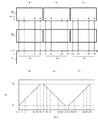
従って、TFTパネル11の入出力端子D(1)〜D(576)と、電流源部161の接続端子P161(1)〜P161(96)とが、ブロック毎に、正順、逆順に、順次、接続されると、入出力端子D(1)〜D(576)の端子電位Vs(1)〜Vs(576)は、図11に示すような特性を示すことになる。
Accordingly, the input / output terminals D (1) to D (576) of the
このように、電流源161a(1)〜161a(p)の特性の偏差に基づいて、端子電位Vs(1)〜Vs(p)にV1〜V2の差が生じていたとしても、入出力端子D(1)〜D(m)に対する端子電位Vs(1)〜Vs(m)における、隣接するブロックの境界における両ブロックの入出力端子に対応する端子電位Vsの間、例えば、ブロック番号b=1の入出力端子D(p)とブロック番号b=2の入出力端子D(p+1)に対する端子電圧Vs(p)とVs(p+1)との間、に段差が生じないようにすることができる。
As described above, even if the difference between V1 and V2 occurs in the terminal potentials Vs (1) to Vs (p) based on the deviation of the characteristics of the
補正演算部132は、各画素11(i,j)に対応する差分電圧Vdef(i)を行毎に補正データ記憶部131から読み出し、読み出した差分電圧Vdef(i)に基づいて各画素11(i,j)のトランジスタT3の閾値電圧を求め、補正データ記憶部131に記憶する。
The
次に、表示装置1に外部から映像信号Imageが供給されて、TFTパネル11に映像信号に応じた画像情報を表示する時の動作について説明する。
このとき、表示信号生成回路12は、供給された映像信号Imageから表示データPic、同期信号Syncを取得してシステムコントローラ13に供給する。そして、システムコントローラ13は、表示信号生成回路12から供給された表示データPicを、画素11(i,j)毎に、補正データ記憶部131に記憶する。
Next, an operation when a video signal Image is supplied from the outside to the
At this time, the display
システムコントローラ13は、補正演算部132が、すべての画素11(i,j)について、補正した電圧データVdataを補正データ記憶部131に記憶すると、書き込み処理を制御する。
When the
システムコントローラ13は、データドライバ16に切換制御信号Csw1(open)とCsw2(close)とを供給する。
The
システムコントローラ13は、セレクトドライバ14にスタート信号Spを供給する。
The
セレクトドライバ14は、システムコントローラ13からスタート信号Spが供給されて動作を開始し、システムコントローラ13から供給されたクロック信号CLKに従い、順次、第1行目の画素11(1,1)〜11(576,1)、・・・、第n行目の画素11(1,n)〜11(576,n)に、Hiレベルの信号Vselect(j)を出力する。
The
データドライバ16のスイッチSw1(1)〜Sw1(576)は、システムコントローラ13から切換制御信号Csw1(open)が供給されて開き、それぞれ、TFTパネル11の入出力端子D(1)〜D(576)と電流源部161の接続端子P161(1)〜(96)との間を遮断する。
The switches Sw1 (1) to Sw1 (576) of the
スイッチSw2(1)〜Sw2(576)は、システムコントローラ13から切換制御信号Csw1(open)が供給されて閉じ、それぞれ、データ出力部164の出力端子P164(1)〜P164(576)と、入出力端子D(1)〜D(576)と、を接続する。
The switches Sw2 (1) to Sw2 (576) are closed when the switching control signal Csw1 (open) is supplied from the
システムコントローラ13における補正演算部132は、表示信号生成回路12から表示データPicが供給されると、補正データ記憶部131から、画素(i,j)毎に、閾値電圧Vthを読み出す。そして、補正演算部132は、読み出した閾値電圧Vthに基づいて表示データPicを補正した電圧データVdataを取得して、Vdata(1)〜Vdata(576)として、順次、データドライバ16に出力する。
When the display data Pic is supplied from the display
データドライバ16のデータ出力部164は、システムコントローラ13から、第1行目の電圧データVdata(1)〜Vdata(576)が供給されると、これらの電圧データVdata(1)〜Vdata(576)をアナログの電圧信号Sv(1)〜Sv(576)に変換する。
When the voltage data Vdata (1) to Vdata (576) of the first row is supplied from the
そして、データ出力部164は、変換した電圧信号Sv(1)〜Sv(576)を、それぞれ、スイッチSw2(1)〜Sw2(576)を介して、TFTパネル11の各入出力端子D(1)〜D(576)に出力する。
Then, the
セレクトドライバ14が第1行目のセレクトラインLs(1)にHiレベルの信号Vselect(1)を出力すると、第1行目の画素11(1,1)〜11(576,1)のキャパシタC1に、それぞれ、電圧信号Sv(1)〜Sv(576)に対応する電圧が書き込まれる。
When the
同様にして、データドライバ16は、第2行目の画素11(1,2)〜11(576,2),・・・,第n行目の画素11(1,n)〜11(576,n)のキャパシタC1に電圧信号Sv(1)〜Sv(576)に対応する電圧を書き込む。
Similarly, the
書き込みが終了すると、システムコントローラ13は、発光動作を制御する。
セレクトドライバ14は、Loレベルの信号Vselect(1)〜Vselect(n)を、それぞれ、セレクトラインLs(1)〜Ls(n)に出力する。
When the writing is completed, the
The
セレクトセレクトラインLs(1)〜Ls(n)の信号レベルがLoレベルになると、すべての画素11(i,j)のトランジスタT1,T2はオフする。 When the signal level of the select line Ls (1) to Ls (n) becomes Lo level, the transistors T1 and T2 of all the pixels 11 (i, j) are turned off.
システムコントローラ13は、電源ドライバ15に、電圧制御信号Cv(H)を供給する。電源ドライバ15は、システムコントローラ13から、この電圧制御信号Cv(H)が供給されて、電圧VH(=+15V)の信号Vsource(1)〜Vsource(n)を、電圧ラインLv(1)〜Lv(n)に出力する。
The
電圧ラインLv(1)〜Lv(n)の電圧がVHになると、各画素11(i,j)のトランジスタT3は、各キャパシタC1が保持した電圧をゲート電圧Vgsとして、この信号ゲート電圧Vgsに対応する電流を有機EL素子111に供給する。
When the voltage of the voltage lines Lv (1) to Lv (n) becomes VH, the transistor T3 of each pixel 11 (i, j) uses the voltage held by each capacitor C1 as the gate voltage Vgs, and this signal gate voltage Vgs. A corresponding current is supplied to the
そして、各有機EL素子111は、この電流が流れることにより、この電流の電流値に対応する輝度で発光する。
Each
以上説明したように、本実施形態によれば、切換部163は、ブロック番号bが奇数の場合は、それぞれ、TFTパネル11の入出力端子D((b−1)×p+k)と、電流源部161の接続端子P161(k)とを接続する。
As described above, according to the present embodiment, when the block number b is an odd number, the
また、切換部163は、ブロック番号bが偶数の場合は、それぞれ、TFTパネル11の入出力端子D((b−1)×p+k)と、電流源部161の接続端子P161(p−k+1)と、を接続するように構成されている。
Further, when the block number b is an even number, the
従って、入出力端子D(1)〜D(m)と、接続端子P161(1)〜P161(p)と、の接続が、ブロック番号bが奇数から偶数、又は、偶数から奇数に切り換わるとき、電流源部161の電流源161a(1)〜161a(p)に電流値の偏差がある場合でも、隣接する入出力端子D(i)間で計測された端子電位Vsの段差を抑制することができる。このため、表示品位の低下を抑制することができる。
Accordingly, when the connection between the input / output terminals D (1) to D (m) and the connection terminals P161 (1) to P161 (p) is switched from the odd number to the even number, or from the even number to the odd number. Even when the
尚、本発明を実施するにあたっては、種々の形態が考えられ、上記実施形態に限られるものではない。 In carrying out the present invention, various forms are conceivable and the present invention is not limited to the above embodiment.
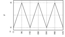
例えば、総ブロック数Bが偶数である場合には、図12に示すように、データドライバ16が2つのデータドライバ16−1,16−2によって構成されてもよい。
For example, when the total block number B is an even number, the
この場合、データドライバ16−1,16−2がTFTパネル11に接続される。各データドライバ16−1,16−2が同じ特性及び構成を有する場合、隣接するデータドライバ16−1,16−2の境界における両データドライバ16−1,16−2の入出力端子に対応する端子電位Vsの間にも段差が生じないようにすることができる。
In this case, the data drivers 16-1 and 16-2 are connected to the
すなわち、例えば、m=576、p=96として、上記のように、切換部163が、ブロック毎に、正順、逆順に切り換えるようにし、総ブロック数Bが偶数(B=6)である場合、データドライバ16−1、16−2の電圧計163v(1)〜(96)が計測した端子電位Vs(1)〜Vs(1152)は、図13に示すような特性を示すことになる。これにより、隣接するデータドライバ間においても段差が生じなくなる。なお、図12においては2つのデータドライバ16−1,16−2を備えるものとしたが、更に、3つ以上の複数のデータドライバを備えるものであってもよい。
That is, for example, when m = 576 and p = 96, as described above, the
また、表示装置1は、図14に示すようにデータドライバがデータドライバ本体部16aと、測定部16bと、からなるものであってもよい。
Further, as shown in FIG. 14, in the
データドライバ本体部16aは、データ出力部164を備える。測定部16bは、電流源部161と、測定部162と、切換部163と、を備える。
The data driver main body 16a includes a
データドライバ本体部16aと測定部16bは、分離されて、例えば別チップで構成されて、実装されているものであってもよい。
The data driver main body 16a and the
次に、上記実施形態では、データドライバ16が電流供給電圧計測方式に従って構成されているものとして説明した。しかし、データドライバ16は、このような構成に限られるものではなく、例えば、図15に示すような電圧印加電流測定方式に従って構成されたものでもよい。
Next, in the above embodiment, the
図15に示すデータドライバ26は、電圧源部261と、測定部262と、切換部163と、スイッチSw1(1)〜Sw1(m),Sw2(1)〜Sw2(m)と、データ出力部164と、を備える。
15 includes a
電圧源部261は、電圧源261v(1)〜261v(p)を備えたものである。電圧源261V(1)〜261v(p)は、データラインLd(i)に電圧を印加するものである。
The
電圧源部261は、p個の接続端子P261(1)〜P261(p)を有し、電圧源261v(1)〜261v(p)の負極は、それぞれ、この接続端子P261(1)〜P261(p)に接続される。
The
また、電圧源261v(1)〜261v(p)の正極は電圧Vssの電位に接続される。 The positive electrodes of the voltage sources 261v (1) to 261v (p) are connected to the potential of the voltage Vss.
測定部262は、m個の電流計262a(1)〜262a(m)を備えたものである。電流計262a(1)〜262a(m)は、それぞれ、データラインLd(1)〜Ld(m)に流れる電流Idの電流値を計測するものである。
The
電流計262a(1)〜262a(m)は、それぞれ、スイッチSw1(1)〜Sw1(m)の電流下流側端子とスイッチSw3(1)〜Sw3(m)の電流上流側端子との間に介挿され、計測した電流Idの電流値をシステムコントローラ13に出力する。
The
また、図4に示すデータドライバ16は、代わりに、図16に示すような電流源&測定部361を備えたデータドライバ36であってもよい。
Further, the
電流源&測定部361は、電流源361a(1)〜361a(p)と、電圧計361v(1)〜361v(p)とを備えたものである。
The current source &
電流源361a(1)〜361a(p)は、それぞれ、図4に示す電流源161a(1)〜161a(p)と同等のものである。また、電圧計361v(1)〜361v(p)は、それぞれ、図4に示す電圧計162a(1)〜162a(m)と同等のものである。
The
次に、図4に示すデータドライバ16は、図17に示すような構成のものであってもよい。このデータドライバ46は、切換部163と、データ出力部164と、電圧源部&測定部461と、を備えたものである。
Next, the
切換部163とデータ出力部164とは、それぞれ、図4に示す切換部163とデータ出力部164と同様のものである。
電圧源&測定部461は、電圧源461v(1)〜461v(p)と、電流計461a(1)〜461a(p)とを備えたものである。すなわち、電流源&測定部461は、電圧源461v(1)〜461v(p)の各々に対応して電流計461a(1)〜461a(p)を備えて、電圧源461a(1)〜461a(p)の数と電流計461a(1)〜461a(p)の数を同じとしたものである。
Voltage source and measuring
この電圧源461v(1)〜461v(p)は、それぞれ、図15に示す電圧源261v(1)〜261v(p)と同等のものである。また、電流計461a(1)〜461a(p)は、それぞれ、図15に示す電圧計262a(1)〜262a(m)と同等のものである。
The voltage sources 461v (1) to 461v (p) are equivalent to the voltage sources 261v (1) to 261v (p) shown in FIG. The ammeters 461a (1) to 461a (p) are equivalent to the
また、上記実施形態においては、電流源部161の各電流源161a(1)〜161a(p)の特性の偏差や電圧源部261の各電圧源261v(1)〜261v(p)の特性の偏差によって、各電圧計162v(i)が計測した電圧値や各電流計262a(i)が計測した電流値が変化する場合について説明した。
Moreover, in the said embodiment, the deviation of the characteristic of each
しかし、仮に各画素や各電流源、各電圧源の特性が揃っていたとしても、各電圧計や電流計の特性が揃っていない場合には、各電圧計や各電流計により得られる電圧値や電流値に、図10(d)に示したのと同様の変化が生じることになる。 However, even if the characteristics of each pixel, each current source, and each voltage source are uniform, if the characteristics of each voltmeter or ammeter are not uniform, the voltage value obtained by each voltmeter or each ammeter As a result, a change similar to that shown in FIG.
そこで、例えば、図4における電流源部161を測定部に置き換え、測定部162を電流源部に置き換えるようにしてもよい。
Therefore, for example, the
この場合の構成を図18に示す。図18に示すデータドライバ56は、切換部163と、データ出力部164と、電流源部561と、測定部562と、を備える。
The configuration in this case is shown in FIG. The
切換部163とデータ出力部164とは、それぞれ、図4に示す切換部163とデータ出力部164と同様のものである。
電流源部561は、電流源561a(1)〜561a(m)を備えたものである。測定部562は、電圧計562v(1)〜562v(p)を備えたものである。
The
そして、切換部163は、接続順序を交互に変えて、測定部562の各電圧計562v(1)〜562v(p)を接続する。
Then, the
このように構成されると、各電圧計562v(1)〜562v(p)の特性が揃っていない場合でも、測定した電圧値の偏差を抑制することができる。
If comprised in this way, even when the characteristics of each
また、例えば、図15に示す電圧源部261を測定部に置き換え、測定部262を電圧源部に置き換えるようにしてもよい。
Further, for example, the
この場合の構成を図19に示す。図19に示すデータドライバ66は、切換部163と、データ出力部164と、電圧源部661と、測定部662と、を備える。
The configuration in this case is shown in FIG. The data driver 66 illustrated in FIG. 19 includes a
切換部163とデータ出力部164とは、それぞれ、図4に示す切換部163とデータ出力部164と同様のものである。
電圧源部661は、電圧源661v(1)〜661v(m)を備えたものである。測定部662は、電流計662a(1)〜662a(p)を備えたものである。
The
そして、切換部163は、接続順序を交互に変えて、測定部の各電流計662a(1)〜662a(p)と電圧源661v(1)〜661v(m)とを接続する。
Then, the
このように構成されると、各電流計662a(1)〜662a(p)の特性が揃っていない場合でも、測定した電流値の偏差を抑制することができる。 If comprised in this way, even when the characteristic of each ammeter 662a (1)-662a (p) is not uniform, the deviation of the measured electric current value can be suppressed.
1・・・表示装置、11・・・TFTパネル、D(1)〜D(m)・・・入出力端子(TFTパネル)、11(i,j)・・・画素、12・・・表示信号生成回路、13・・・システムコントローラ、16・・・データドライバ、161・・・電流源部、P161(1)〜P161(p)・・・接続端子、162・・・測定部、163・・・切換部、163d・・・デコーダ、Sw1(1)〜Sw1(m),Sw2(1)〜Sw2(m),Sw3(1)〜Sw3(m)・・・スイッチ
DESCRIPTION OF
Claims (22)
前記複数の入出力端子の数より少ない所定の数の接続端子を有する接続ユニットと、
前記各接続端子と前記各入出力端子との接続を切り換える接続切換部と、
を備え、
前記接続切換部は、前記複数の入出力端子を互いに隣接する前記所定の数の前記入出力端子毎の複数のブロックに分割し、互いに隣接する2つの前記ブロックにおける一方のブロックと他方のブロックに対し、前記接続ユニットの前記各接続端子と前記一方のブロックの前記各入出力端子との接続順序と、前記接続ユニットの前記各接続端子と前記他方のブロックの前記各入出力端子との接続順序とを、互いに逆の順序に設定し、前記一方のブロックに属する第1の入出力端子と前記他方のブロックに属し前記第1の入出力端子と隣接する第2の入出力端子に対して、前記所定の数の接続端子の何れかの同じ前記接続端子を接続し、
前記接続ユニットは、測定用の電流を出力する電流源、測定用の電圧を出力する電圧源、電圧値を測定する電圧計及び電流値を測定する電流計の何れかを、前記複数の接続端子の各々に対応して複数備え、前記各接続端子と前記各ブロックの前記各入出力端子とが接続されたとき、(1)前記接続ユニットが接続された前記各ブロックの前記各入出力端子への前記測定用の電圧の供給又は前記測定用の電流の供給、(2)前記接続ユニットが接続された前記各ブロックの前記各入出力端子の電圧の電圧値の測定又は前記各入出力端子に流れる電流の電流値の測定、の何れかを行うことを特徴とする画素駆動装置。 A pixel driving device for driving a pixel array having a plurality of input / output terminals and a plurality of pixels connected to the plurality of input / output terminals,
A connection unit having a predetermined number of connection terminals less than the number of the plurality of input / output terminals;
A connection switching section for switching the connection between each connection terminal and each input / output terminal;
With
The connection switching unit divides the plurality of input / output terminals into a plurality of blocks for each of the predetermined number of the input / output terminals adjacent to each other, and is divided into one block and the other block of the two adjacent blocks. On the other hand, the connection order of the connection terminals of the connection unit and the input / output terminals of the one block, and the connection order of the connection terminals of the connection unit and the input / output terminals of the other block Are set in a reverse order to each other, with respect to the first input / output terminal belonging to the one block and the second input / output terminal belonging to the other block and adjacent to the first input / output terminal, Connecting the same connection terminal of any of the predetermined number of connection terminals;
The connection unit includes any one of a current source that outputs a current for measurement, a voltage source that outputs a voltage for measurement, a voltmeter that measures a voltage value, and an ammeter that measures a current value. When each connection terminal and each input / output terminal of each block are connected, (1) To each input / output terminal of each block to which the connection unit is connected Supply of the voltage for measurement or supply of the current for measurement; (2) measurement of the voltage value of the input / output terminals of the blocks to which the connection unit is connected or the input / output terminals; A pixel driving device that performs any one of measurement of a current value of a flowing current .
接続切換部は、
前記接続ユニットの前記各接続端子と前記複数のブロックにおける奇数番目の前記ブロックの前記各入出力端子とを前記接続ユニットの前記各接続端子の配列順序に沿った順序で接続する第1のスイッチ群と、
前記接続ユニットの前記各接続端子と前記複数のブロックにおける偶数番目の前記ブロックの前記各入出力端子とを前記接続ユニットの前記各接続端子の配列順序と逆の順序で接続する第2のスイッチ群と、
前記制御部から供給される切換制御信号に基づいて、前記第1のスイッチ群及び前記第2のスイッチ群の開閉を制御する開閉制御部と、
を備えたことを特徴とする請求項1に記載の画素駆動装置。 A control unit that supplies a switching control signal for switching the connection between the connection terminals of the connection unit and the input / output terminals of the blocks to the connection switching unit;
The connection switching part
A first switch group that connects the connection terminals of the connection unit and the input / output terminals of the odd-numbered blocks in the plurality of blocks in an order according to the arrangement order of the connection terminals of the connection unit. When,
A second switch group for connecting the connection terminals of the connection unit and the input / output terminals of the even-numbered blocks in the plurality of blocks in an order opposite to the arrangement order of the connection terminals of the connection unit; When,
An open / close control unit that controls opening and closing of the first switch group and the second switch group, based on a switching control signal supplied from the control unit;
The pixel driving apparatus according to claim 1 , further comprising:
前記複数の入出力端子の数より少ない所定の数の接続端子を有する接続ユニットと、
前記各接続端子と前記各入出力端子との接続を切り換える接続切換部と、
を備え、
前記接続切換部は、前記複数の入出力端子を互いに隣接する前記所定の数の前記入出力端子毎の複数のブロックに分割し、互いに隣接する2つの前記ブロックにおける一方のブロックと他方のブロックに対し、前記接続ユニットの前記各接続端子と前記一方のブロックの前記各入出力端子との接続順序と、前記接続ユニットの前記各接続端子と前記他方のブロックの前記各入出力端子との接続順序とを、互いに逆の順序に設定し、前記一方のブロックに属する第1の入出力端子と前記他方のブロックに属し前記第1の入出力端子と隣接する第2の入出力端子に対して、前記所定の数の接続端子の何れかの同じ前記接続端子を接続し、
前記接続ユニットは、測定用の電流を出力する電流源、測定用の電圧を出力する電圧源、電圧値を測定する電圧計及び電流値を測定する電流計の何れかを、前記複数の接続端子の各々に対応して複数備え、前記各接続端子と前記各ブロックの前記各入出力端子とが接続されたとき、(1)前記接続ユニットが接続された前記各ブロックの前記各入出力端子への前記測定用の電圧の供給又は前記測定用の電流の供給、(2)前記接続ユニットが接続された前記各ブロックの前記各入出力端子の電圧の電圧値の測定又は前記各入出力端子に流れる電流の電流値の測定、の何れかを行うことを特徴とする発光装置。 A pixel array having a plurality of input / output terminals and a plurality of pixels having light emitting elements connected to the plurality of input / output terminals;
A connection unit having a predetermined number of connection terminals less than the number of the plurality of input / output terminals;
A connection switching section for switching the connection between each connection terminal and each input / output terminal;
With
The connection switching unit divides the plurality of input / output terminals into a plurality of blocks for each of the predetermined number of the input / output terminals adjacent to each other, and is divided into one block and the other block of the two adjacent blocks. On the other hand, the connection order of the connection terminals of the connection unit and the input / output terminals of the one block, and the connection order of the connection terminals of the connection unit and the input / output terminals of the other block Are set in a reverse order to each other, with respect to the first input / output terminal belonging to the one block and the second input / output terminal belonging to the other block and adjacent to the first input / output terminal, Connecting the same connection terminal of any of the predetermined number of connection terminals;
The connection unit includes any one of a current source that outputs a current for measurement, a voltage source that outputs a voltage for measurement, a voltmeter that measures a voltage value, and an ammeter that measures a current value. When each connection terminal and each input / output terminal of each block are connected, (1) To each input / output terminal of each block to which the connection unit is connected Supply of the voltage for measurement or supply of the current for measurement; (2) measurement of the voltage value of the input / output terminals of the blocks to which the connection unit is connected or the input / output terminals; A light-emitting device that performs any one of measurement of a current value of a flowing current .
前記各画素は、電流路の一端が前記発光素子の一端に接続されるとともに前記各データラインに電気的に接続され、該電流路の他端に所定の電圧値の電源電圧が印加されて、前記発光素子に供給する電流を制御する駆動トランジスタを有し、
前記測定部は、前記接続ユニットより、前記接続切換部を介して、オン状態とされた前記各画素の前記駆動トランジスタの電流路に電流が流れるときの前記各入出力端子の電位の値又は前記各接続端子から前記接続切換部及び前記各入出力端子を介して前記各データラインに流れる電流の電流値を取得することを特徴とする請求項14乃至16のいずれか1項に記載の発光装置。 The pixel array has a plurality of data lines connected to each of the plurality of input / output terminals,
Each pixel has one end of a current path connected to one end of the light emitting element and electrically connected to each data line, and a power supply voltage having a predetermined voltage value is applied to the other end of the current path, A driving transistor for controlling a current supplied to the light emitting element;
The measuring unit is configured such that the current value of each input / output terminal when current flows from the connection unit to the current path of the drive transistor of each pixel that is turned on from the connection unit or the connection switching unit, or The light emitting device according to any one of claims 14 to 16 , wherein a current value of a current flowing through each data line is acquired from each connection terminal via the connection switching unit and each input / output terminal. .
前記複数の入出力端子を互いに隣接する前記所定の数の入出力端子毎の複数のブロックに分割し、互いに隣接する2つの前記ブロックにおける一方のブロックと他方のブロックに対し、前記接続ユニットの前記各接続端子を、前記一方のブロックの前記各入出力端子と、前記他方のブロックの前記各入出力端子とに、互いに逆の順序で順次接続し、
前記一方のブロックに属する第1の入出力端子と前記他方のブロックに属し前記第1の入出力端子と隣接する第2の入出力端子に、前記所定の数の接続端子の何れかの特定の前記接続端子を接続し、
前記接続ユニットに、測定用の電流を出力する電流源、測定用の電圧を出力する電圧源、電圧値を測定する電圧計、電流値を測定する電流計、の何れかを前記複数の接続端子の各々に対応して複数設けて、前記接続ユニットの前記各接続端子と前記各ブロックの前記各入出力端子とを接続して、(1)前記接続ユニットを接続した前記各ブロックの前記各入出力端子への測定用の電圧又は電流の供給、(2)前記接続ユニットを接続した前記各ブロックの前記各入出力端子の電圧の電圧値又は前記各入出力端子に流れる電流の電流値の測定、の何れかを行うことを特徴とする画素駆動装置の接続ユニット接続方法。 A connection having a predetermined number of connection terminals smaller than the number of the plurality of input / output terminals in the plurality of input / output terminals of the pixel driving device for driving a pixel array having a plurality of input / output terminals connected to the plurality of pixels. A connection unit connection method of a pixel driving device for connecting units,
The plurality of input / output terminals are divided into a plurality of blocks for each of the predetermined number of input / output terminals adjacent to each other, and one of the two blocks adjacent to each other and the other block are connected to the block of the connection unit. each connection terminal, wherein each input and output terminals of the one block, the on each input and output terminals of the other block, sequentially connected in reverse order to each other,
A first input / output terminal belonging to the one block and a second input / output terminal belonging to the other block and adjacent to the first input / output terminal ; Connect the connection terminals,
The plurality of connection terminals include any one of a current source that outputs a measurement current, a voltage source that outputs a measurement voltage, a voltmeter that measures a voltage value, and an ammeter that measures a current value. A plurality of terminals corresponding to each of the connection units, and the connection terminals of the connection unit and the input / output terminals of the blocks are connected. Supply of measurement voltage or current to the output terminal, (2) Measurement of voltage value of each input / output terminal of each block connected to the connection unit or current value of current flowing through each input / output terminal Any one of the above, a connection unit connection method for a pixel driving device.
p(pは自然数、p<m)個の接続端子P(k)(k=1〜p)を有する接続ユニットと、
前記表示パネルの各入出力端子D(i)のいずれかと前記接続ユニットの各接続端子P(k)とを接続する接続切換部と、を備え、
前記接続切換部は、
前記表示パネルの入出力端子D(i)を互いに隣接するp個の前記入出力端子D(i)毎の複数のブロックに分割し、分割したブロックのブロック数をb(b=1〜m/p)として、
前記ブロック数bが奇数の奇数ブロックの前記入出力端子D((b−1)×p+k)に対する前記各接続端子P(k)の接続順序と、前記ブロック数bが偶数の偶数ブロックの前記入出力端子D((b−1)×p+k)に対する前記各接続端子P(k)の接続順序と、を互いに逆の順序に設定して、
前記奇数ブロックの前記入出力端子D((b−1)×p+k)と前記接続ユニットの接続端子P(k)とを接続したときは、前記偶数ブロックの前記表示パネルの入出力端子D((b−1)×p+k)と前記接続ユニットの接続端子P(p−k+1)とを接続し、
前記偶数ブロックの前記入出力端子D((b−1)×p+k)と前記接続ユニットの接続端子P(k)とを接続したときは、前記奇数ブロックの前記表示パネルの入出力端子D((b−1)×p+k)と前記接続ユニットの接続端子P(p−k+1)とを接続し、
前記接続ユニットは、測定用の電流を出力する電流源、測定用の電圧を出力する電圧源、電圧値を測定する電圧計、電流値を測定する電流計、の何れかを前記各接続端子に対応してp個備え、前記各接続端子と前記各ブロックの前記各入出力端子とが接続されたとき、(1)前記接続ユニットが接続された前記各ブロックの前記各入出力端子D((b−1)×p+k)への前記測定用の電圧の供給又は前記測定用の電流の供給、(2)前記接続ユニットが接続された前記各ブロックの前記各入出力端子D((b−1)×p+k)の電圧の電圧値の測定又は前記各入出力端子D((b−1)×p+k)に流れる電流の電流値の測定、の何れかを行うことを特徴とする表示装置。 a display panel having m (m is a natural number) input / output terminals D (i) (i = 1 to m);
a connection unit having p (p is a natural number, p <m) connection terminals P (k) (k = 1 to p),
A connection switching unit for connecting any one of the input / output terminals D (i) of the display panel to each of the connection terminals P (k) of the connection unit;
The connection switching unit is
The input / output terminal D (i) of the display panel is divided into a plurality of blocks for each of the p input / output terminals D (i) adjacent to each other, and the number of divided blocks is b (b = 1 to m / p)
The connection order of the connection terminals P (k) to the input / output terminals D ((b−1) × p + k) of the odd-numbered block having the odd number of blocks b, and the input of the even-numbered block having the even number of blocks b. The connection order of the connection terminals P (k) with respect to the output terminal D ((b−1) × p + k) is set in the reverse order to each other,
When connecting the input terminal D of the odd block ((b-1) × p + k) and the connecting unit of the connection terminal P (k) is input and output terminal D of the display panel of the even block (( b-1) × p + k) and the connection terminal P (p−k + 1) of the connection unit are connected,
When connecting the input terminal D of the even block ((b-1) × p + k) and the connecting unit of the connection terminal P (k) is input and output terminal D of the display panel of the odd block (( b-1) × p + k ) and the connection terminal P of the connection unit (p-k + 1) and connected to,
The connection unit is configured such that any one of a current source that outputs a measurement current, a voltage source that outputs a measurement voltage, a voltmeter that measures a voltage value, and an ammeter that measures a current value is connected to each connection terminal. Correspondingly, p units are provided, and when each connection terminal is connected to each input / output terminal of each block, (1) each input / output terminal D (( b-1) supply of voltage for measurement or supply of current for measurement to xp + k), (2) each input / output terminal D ((b-1) of each block to which the connection unit is connected ) × p + k), or a current value of a current flowing through each of the input / output terminals D ((b−1) × p + k) .
前記接続切換部は、
一端が前記表示パネルの前記奇数ブロックの入出力端子D((b−1)×p+k)に接続され、他端が前記接続ユニットの接続端子P(k)に接続された第1のスイッチと、
一端が前記表示パネルの前記偶数ブロックの入出力端子D((b−1)×p+k)に接続され、他端が前記接続ユニットの接続端子P(p−k+1)に接続された第2のスイッチと、
前記制御部から供給された切換制御信号に基づいて、前記第1のスイッチと前記第2のスイッチとの開閉を制御する開閉制御部と、を備えた、
ことを特徴とする請求項20に記載の表示装置。 A controller that supplies the connection switching unit with a switching control signal for switching the input / output terminal D ((b-1) × p + k) connected to the connection unit to the odd block or the even block ;
The connection switching unit is
A first switch having one end connected to the input / output terminal D ((b−1) × p + k) of the odd-numbered block of the display panel and the other end connected to the connection terminal P (k) of the connection unit;
A second switch having one end connected to the input / output terminal D ((b−1) × p + k) of the even-numbered block of the display panel and the other end connected to the connection terminal P (p−k + 1) of the connection unit When,
An open / close control unit that controls opening and closing of the first switch and the second switch based on a switching control signal supplied from the control unit;
The display device according to claim 20 .
前記接続切換部は、
一端が前記表示パネルの前記偶数ブロックの入出力端子D((b−1)×p+k)に接続され、他端が前記接続ユニットの接続端子P(k)に接続された第1のスイッチと、
一端が前記表示パネルの前記奇数ブロックの入出力端子D((b−1)×p+k)に接続され、他端が前記接続ユニットの接続端子P(p−k+1)に接続された第2のスイッチと、
前記制御部から供給された切換制御信号に基づいて、前記第1のスイッチと前記第2のスイッチとの開閉を制御する開閉制御部と、を備えた、
ことを特徴とする請求項20に記載の表示装置。 A controller that supplies the connection switching unit with a switching control signal for switching the input / output terminal D ((b-1) × p + k) connected to the connection unit to the odd block or the even block ;
The connection switching unit is
A first switch having one end connected to the input / output terminal D ((b−1) × p + k) of the even-numbered block of the display panel and the other end connected to the connection terminal P (k) of the connection unit;
A second switch having one end connected to the input / output terminal D ((b−1) × p + k) of the odd-numbered block of the display panel and the other end connected to the connection terminal P (p−k + 1) of the connection unit When,
An open / close control unit that controls opening and closing of the first switch and the second switch based on a switching control signal supplied from the control unit;
The display device according to claim 20 .
Priority Applications (7)
| Application Number | Priority Date | Filing Date | Title |
|---|---|---|---|
| JP2009046147A JP5083245B2 (en) | 2008-09-30 | 2009-02-27 | Pixel drive device, light emitting device, display device, and connection unit connection method for pixel drive device |
| PCT/JP2009/067290 WO2010038882A1 (en) | 2008-09-30 | 2009-09-28 | Pixel drive device, luminescence device, and method of connecting a connection unit in the pixel drive device |
| EP09788088.4A EP2329486B1 (en) | 2008-09-30 | 2009-09-28 | Pixel drive device, luminescence device, and method of connecting a connection unit in the pixel drive device |
| CN200980101171.0A CN101878500B (en) | 2008-09-30 | 2009-09-28 | Pixel driving device, light emitting device and method for connecting connection units in the pixel driving device |
| KR1020107011874A KR101186397B1 (en) | 2008-09-30 | 2009-09-28 | Pixel drive device, luminescence device, and method of connecting a connection unit in the pixel drive device |
| TW098132825A TWI421825B (en) | 2008-09-30 | 2009-09-29 | Pixel drive device, luminescence device, and method of connecting connection unit in pixel drive device |
| US12/570,278 US20100079420A1 (en) | 2008-09-30 | 2009-09-30 | Pixel drive device, luminescence device, and method of connecting connection unit in pixel drive device |
Applications Claiming Priority (3)
| Application Number | Priority Date | Filing Date | Title |
|---|---|---|---|
| JP2008255550 | 2008-09-30 | ||
| JP2008255550 | 2008-09-30 | ||
| JP2009046147A JP5083245B2 (en) | 2008-09-30 | 2009-02-27 | Pixel drive device, light emitting device, display device, and connection unit connection method for pixel drive device |
Publications (2)
| Publication Number | Publication Date |
|---|---|
| JP2010107936A JP2010107936A (en) | 2010-05-13 |
| JP5083245B2 true JP5083245B2 (en) | 2012-11-28 |
Family
ID=41272162
Family Applications (1)
| Application Number | Title | Priority Date | Filing Date |
|---|---|---|---|
| JP2009046147A Expired - Fee Related JP5083245B2 (en) | 2008-09-30 | 2009-02-27 | Pixel drive device, light emitting device, display device, and connection unit connection method for pixel drive device |
Country Status (7)
| Country | Link |
|---|---|
| US (1) | US20100079420A1 (en) |
| EP (1) | EP2329486B1 (en) |
| JP (1) | JP5083245B2 (en) |
| KR (1) | KR101186397B1 (en) |
| CN (1) | CN101878500B (en) |
| TW (1) | TWI421825B (en) |
| WO (1) | WO2010038882A1 (en) |
Families Citing this family (8)
| Publication number | Priority date | Publication date | Assignee | Title |
|---|---|---|---|---|
| TWI470942B (en) * | 2010-07-30 | 2015-01-21 | 明陽半導體股份有限公司 | Driving circuit, decoding circuit and decoding method thereof |
| KR102029319B1 (en) * | 2013-06-19 | 2019-10-08 | 삼성디스플레이 주식회사 | Organic Light Emitting Display Device and Driving Method Thereof |
| KR102180792B1 (en) | 2014-07-30 | 2020-11-20 | 삼성디스플레이 주식회사 | Organic light emitting display device and method of driving an organic light emitting display device |
| JP2017058522A (en) * | 2015-09-16 | 2017-03-23 | 双葉電子工業株式会社 | Display drive device, display device and display drive method |
| TWI613639B (en) * | 2016-09-06 | 2018-02-01 | 友達光電股份有限公司 | Switchable pixel circuit and driving method thereof |
| CN107331343B (en) * | 2017-07-07 | 2019-08-02 | 深圳市明微电子股份有限公司 | A kind of display screen and data transfer path planing method, resolution ratio expanding method |
| JP2019074688A (en) * | 2017-10-18 | 2019-05-16 | シャープ株式会社 | Image signal conditioning circuit for drive circuit for display, image signal conditioning method, and image signal conditioning program |
| CN114170984B (en) * | 2021-11-30 | 2023-06-23 | 重庆惠科金渝光电科技有限公司 | Display panel driving method and display panel |
Family Cites Families (15)
| Publication number | Priority date | Publication date | Assignee | Title |
|---|---|---|---|---|
| JP4244110B2 (en) * | 2001-05-28 | 2009-03-25 | パイオニア株式会社 | LIGHT EMITTING PANEL DRIVING DEVICE AND PORTABLE TERMINAL DEVICE HAVING LIGHT EMITTING PANEL |
| CN100410786C (en) * | 2001-10-03 | 2008-08-13 | 夏普株式会社 | Active matrix display device, and data line switching circuit, switching section drive circuit, and scanning line drive circuit thereof |
| US6806497B2 (en) * | 2002-03-29 | 2004-10-19 | Seiko Epson Corporation | Electronic device, method for driving the electronic device, electro-optical device, and electronic equipment |
| JP4266682B2 (en) * | 2002-03-29 | 2009-05-20 | セイコーエプソン株式会社 | Electronic device, driving method of electronic device, electro-optical device, and electronic apparatus |
| JP4530622B2 (en) * | 2003-04-10 | 2010-08-25 | Okiセミコンダクタ株式会社 | Display panel drive device |
| JP2004325716A (en) * | 2003-04-24 | 2004-11-18 | Sharp Corp | Driving circuit for displaying color images and display device having the same |
| JP4649332B2 (en) * | 2003-05-07 | 2011-03-09 | 東芝モバイルディスプレイ株式会社 | Current output type semiconductor circuit and display device |
| KR100589381B1 (en) * | 2003-11-27 | 2006-06-14 | 삼성에스디아이 주식회사 | Display device using demultiplexer and driving method thereof |
| JP4239095B2 (en) * | 2004-03-30 | 2009-03-18 | ソニー株式会社 | Flat display device drive circuit and flat display device |
| JP2006184648A (en) * | 2004-12-28 | 2006-07-13 | Pentax Corp | Light emitting display device and driving method of light emitting display device |
| KR100748739B1 (en) * | 2005-01-28 | 2007-08-13 | 도시바 마쯔시따 디스플레이 테크놀로지 컴퍼니, 리미티드 | El display apparatus and method of driving the same |
| JP4592582B2 (en) * | 2005-07-14 | 2010-12-01 | ルネサスエレクトロニクス株式会社 | Data line driver |
| KR100635509B1 (en) * | 2005-08-16 | 2006-10-17 | 삼성에스디아이 주식회사 | Organic electroluminescent display |
| JP4222426B2 (en) * | 2006-09-26 | 2009-02-12 | カシオ計算機株式会社 | Display driving device and driving method thereof, and display device and driving method thereof |
| KR20080064926A (en) * | 2007-01-06 | 2008-07-10 | 삼성전자주식회사 | Display device and driving method thereof |
-
2009
- 2009-02-27 JP JP2009046147A patent/JP5083245B2/en not_active Expired - Fee Related
- 2009-09-28 EP EP09788088.4A patent/EP2329486B1/en not_active Not-in-force
- 2009-09-28 KR KR1020107011874A patent/KR101186397B1/en not_active Expired - Fee Related
- 2009-09-28 WO PCT/JP2009/067290 patent/WO2010038882A1/en not_active Ceased
- 2009-09-28 CN CN200980101171.0A patent/CN101878500B/en not_active Expired - Fee Related
- 2009-09-29 TW TW098132825A patent/TWI421825B/en not_active IP Right Cessation
- 2009-09-30 US US12/570,278 patent/US20100079420A1/en not_active Abandoned
Also Published As
| Publication number | Publication date |
|---|---|
| CN101878500B (en) | 2013-01-23 |
| CN101878500A (en) | 2010-11-03 |
| EP2329486A1 (en) | 2011-06-08 |
| WO2010038882A1 (en) | 2010-04-08 |
| EP2329486B1 (en) | 2016-01-27 |
| TWI421825B (en) | 2014-01-01 |
| JP2010107936A (en) | 2010-05-13 |
| KR101186397B1 (en) | 2012-09-27 |
| US20100079420A1 (en) | 2010-04-01 |
| TW201027485A (en) | 2010-07-16 |
| KR20100077043A (en) | 2010-07-06 |
Similar Documents
| Publication | Publication Date | Title |
|---|---|---|
| US9390652B2 (en) | Organic light emitting display device and driving method thereof | |
| US7944414B2 (en) | Display drive apparatus in which display pixels in a plurality of specific rows are set in a selected state with periods at least overlapping each other, and gradation current is supplied to the display pixels during the selected state, and display apparatus | |
| CN1989539B (en) | Display drive apparatus, display apparatus and drive control method thereof | |
| CN104715717B (en) | Organic light-emitting display device | |
| CN102428508B (en) | Image display device and driving method thereof | |
| US10839754B2 (en) | Organic light emitting display having multiplexer for distributing data voltages | |
| JP5083245B2 (en) | Pixel drive device, light emitting device, display device, and connection unit connection method for pixel drive device | |
| CN101551970B (en) | Light-emitting device, display device and drive control method for light-emitting device | |
| US20110084955A1 (en) | Organic light emitting display | |
| US20090174699A1 (en) | Electroluminescent display devices an active matrix | |
| US20080252217A1 (en) | Pixel, organic light emitting display using the same, and associated methods | |
| JP4816744B2 (en) | Light emitting device, display device, and drive control method of light emitting device | |
| US20080266214A1 (en) | Sub-pixel current measurement for oled display | |
| JP2006516745A (en) | Active matrix display device | |
| TW201220277A (en) | Pixel driving circuit of an organic light emitting diode | |
| TW201333922A (en) | Display device and drive method thereof | |
| US8339384B2 (en) | Display driving apparatus, display apparatus and drive control method for display apparatus | |
| KR20160075891A (en) | Orgainic light emitting display | |
| JP4877261B2 (en) | Display device and drive control method thereof | |
| JP5256973B2 (en) | Pixel driving device, light emitting device, and display device | |
| TWI407826B (en) | Light-emtting device, display device, and method for controlling driving of the light-emitting device |
Legal Events
| Date | Code | Title | Description |
|---|---|---|---|
| A131 | Notification of reasons for refusal |
Free format text: JAPANESE INTERMEDIATE CODE: A131 Effective date: 20120221 |
|
| A521 | Request for written amendment filed |
Free format text: JAPANESE INTERMEDIATE CODE: A523 Effective date: 20120423 |
|
| TRDD | Decision of grant or rejection written | ||
| A01 | Written decision to grant a patent or to grant a registration (utility model) |
Free format text: JAPANESE INTERMEDIATE CODE: A01 Effective date: 20120807 |
|
| A01 | Written decision to grant a patent or to grant a registration (utility model) |
Free format text: JAPANESE INTERMEDIATE CODE: A01 |
|
| A61 | First payment of annual fees (during grant procedure) |
Free format text: JAPANESE INTERMEDIATE CODE: A61 Effective date: 20120820 |
|
| R150 | Certificate of patent or registration of utility model |
Ref document number: 5083245 Country of ref document: JP Free format text: JAPANESE INTERMEDIATE CODE: R150 Free format text: JAPANESE INTERMEDIATE CODE: R150 |
|
| FPAY | Renewal fee payment (event date is renewal date of database) |
Free format text: PAYMENT UNTIL: 20150914 Year of fee payment: 3 |
|
| R250 | Receipt of annual fees |
Free format text: JAPANESE INTERMEDIATE CODE: R250 |
|
| S111 | Request for change of ownership or part of ownership |
Free format text: JAPANESE INTERMEDIATE CODE: R313113 |
|
| R350 | Written notification of registration of transfer |
Free format text: JAPANESE INTERMEDIATE CODE: R350 |
|
| R250 | Receipt of annual fees |
Free format text: JAPANESE INTERMEDIATE CODE: R250 |
|
| R250 | Receipt of annual fees |
Free format text: JAPANESE INTERMEDIATE CODE: R250 |
|
| R250 | Receipt of annual fees |
Free format text: JAPANESE INTERMEDIATE CODE: R250 |
|
| LAPS | Cancellation because of no payment of annual fees |