JP5071377B2 - Compound semiconductor device and manufacturing method thereof - Google Patents
Compound semiconductor device and manufacturing method thereof Download PDFInfo
- Publication number
- JP5071377B2 JP5071377B2 JP2008506071A JP2008506071A JP5071377B2 JP 5071377 B2 JP5071377 B2 JP 5071377B2 JP 2008506071 A JP2008506071 A JP 2008506071A JP 2008506071 A JP2008506071 A JP 2008506071A JP 5071377 B2 JP5071377 B2 JP 5071377B2
- Authority
- JP
- Japan
- Prior art keywords
- layer
- compound semiconductor
- semiconductor device
- gate electrode
- forming
- Prior art date
- Legal status (The legal status is an assumption and is not a legal conclusion. Google has not performed a legal analysis and makes no representation as to the accuracy of the status listed.)
- Active
Links
- 239000004065 semiconductor Substances 0.000 title claims description 144
- 150000001875 compounds Chemical class 0.000 title claims description 136
- 238000004519 manufacturing process Methods 0.000 title claims description 34
- 239000010410 layer Substances 0.000 claims description 267
- 238000000034 method Methods 0.000 claims description 28
- 239000012212 insulator Substances 0.000 claims description 22
- 239000011241 protective layer Substances 0.000 claims description 19
- 239000000758 substrate Substances 0.000 claims description 9
- 238000001039 wet etching Methods 0.000 claims description 9
- 229910002704 AlGaN Inorganic materials 0.000 description 19
- 238000005530 etching Methods 0.000 description 9
- 238000012360 testing method Methods 0.000 description 6
- 230000015556 catabolic process Effects 0.000 description 5
- 230000015572 biosynthetic process Effects 0.000 description 4
- 238000001312 dry etching Methods 0.000 description 4
- 238000005468 ion implantation Methods 0.000 description 4
- 238000002955 isolation Methods 0.000 description 4
- 238000005268 plasma chemical vapour deposition Methods 0.000 description 3
- 238000012545 processing Methods 0.000 description 3
- 230000005533 two-dimensional electron gas Effects 0.000 description 3
- 238000000231 atomic layer deposition Methods 0.000 description 2
- 230000006866 deterioration Effects 0.000 description 2
- 230000005684 electric field Effects 0.000 description 2
- 238000001020 plasma etching Methods 0.000 description 2
- 229910001218 Gallium arsenide Inorganic materials 0.000 description 1
- 206010039203 Road traffic accident Diseases 0.000 description 1
- 239000002253 acid Substances 0.000 description 1
- 239000013078 crystal Substances 0.000 description 1
- 238000002109 crystal growth method Methods 0.000 description 1
- 230000007423 decrease Effects 0.000 description 1
- 230000003247 decreasing effect Effects 0.000 description 1
- 238000011161 development Methods 0.000 description 1
- 230000000694 effects Effects 0.000 description 1
- 230000003993 interaction Effects 0.000 description 1
- 239000002184 metal Substances 0.000 description 1
- 238000002488 metal-organic chemical vapour deposition Methods 0.000 description 1
- 238000012986 modification Methods 0.000 description 1
- 230000004048 modification Effects 0.000 description 1
- 230000002093 peripheral effect Effects 0.000 description 1
- 230000010287 polarization Effects 0.000 description 1
- 230000002250 progressing effect Effects 0.000 description 1
- 230000001681 protective effect Effects 0.000 description 1
- 229910052594 sapphire Inorganic materials 0.000 description 1
- 239000010980 sapphire Substances 0.000 description 1
- 229920006395 saturated elastomer Polymers 0.000 description 1
- 238000004544 sputter deposition Methods 0.000 description 1
- 239000000126 substance Substances 0.000 description 1
Images


Classifications
-
- H—ELECTRICITY
- H01—ELECTRIC ELEMENTS
- H01L—SEMICONDUCTOR DEVICES NOT COVERED BY CLASS H10
- H01L29/00—Semiconductor devices adapted for rectifying, amplifying, oscillating or switching, or capacitors or resistors with at least one potential-jump barrier or surface barrier, e.g. PN junction depletion layer or carrier concentration layer; Details of semiconductor bodies or of electrodes thereof ; Multistep manufacturing processes therefor
- H01L29/66—Types of semiconductor device ; Multistep manufacturing processes therefor
- H01L29/68—Types of semiconductor device ; Multistep manufacturing processes therefor controllable by only the electric current supplied, or only the electric potential applied, to an electrode which does not carry the current to be rectified, amplified or switched
- H01L29/76—Unipolar devices, e.g. field effect transistors
- H01L29/772—Field effect transistors
- H01L29/778—Field effect transistors with two-dimensional charge carrier gas channel, e.g. HEMT ; with two-dimensional charge-carrier layer formed at a heterojunction interface
-
- H—ELECTRICITY
- H01—ELECTRIC ELEMENTS
- H01L—SEMICONDUCTOR DEVICES NOT COVERED BY CLASS H10
- H01L29/00—Semiconductor devices adapted for rectifying, amplifying, oscillating or switching, or capacitors or resistors with at least one potential-jump barrier or surface barrier, e.g. PN junction depletion layer or carrier concentration layer; Details of semiconductor bodies or of electrodes thereof ; Multistep manufacturing processes therefor
- H01L29/02—Semiconductor bodies ; Multistep manufacturing processes therefor
- H01L29/12—Semiconductor bodies ; Multistep manufacturing processes therefor characterised by the materials of which they are formed
- H01L29/20—Semiconductor bodies ; Multistep manufacturing processes therefor characterised by the materials of which they are formed including, apart from doping materials or other impurities, only AIIIBV compounds
- H01L29/201—Semiconductor bodies ; Multistep manufacturing processes therefor characterised by the materials of which they are formed including, apart from doping materials or other impurities, only AIIIBV compounds including two or more compounds, e.g. alloys
- H01L29/205—Semiconductor bodies ; Multistep manufacturing processes therefor characterised by the materials of which they are formed including, apart from doping materials or other impurities, only AIIIBV compounds including two or more compounds, e.g. alloys in different semiconductor regions, e.g. heterojunctions
-
- H—ELECTRICITY
- H01—ELECTRIC ELEMENTS
- H01L—SEMICONDUCTOR DEVICES NOT COVERED BY CLASS H10
- H01L29/00—Semiconductor devices adapted for rectifying, amplifying, oscillating or switching, or capacitors or resistors with at least one potential-jump barrier or surface barrier, e.g. PN junction depletion layer or carrier concentration layer; Details of semiconductor bodies or of electrodes thereof ; Multistep manufacturing processes therefor
- H01L29/02—Semiconductor bodies ; Multistep manufacturing processes therefor
- H01L29/12—Semiconductor bodies ; Multistep manufacturing processes therefor characterised by the materials of which they are formed
- H01L29/26—Semiconductor bodies ; Multistep manufacturing processes therefor characterised by the materials of which they are formed including, apart from doping materials or other impurities, elements provided for in two or more of the groups H01L29/16, H01L29/18, H01L29/20, H01L29/22, H01L29/24, e.g. alloys
- H01L29/267—Semiconductor bodies ; Multistep manufacturing processes therefor characterised by the materials of which they are formed including, apart from doping materials or other impurities, elements provided for in two or more of the groups H01L29/16, H01L29/18, H01L29/20, H01L29/22, H01L29/24, e.g. alloys in different semiconductor regions, e.g. heterojunctions
-
- H—ELECTRICITY
- H01—ELECTRIC ELEMENTS
- H01L—SEMICONDUCTOR DEVICES NOT COVERED BY CLASS H10
- H01L29/00—Semiconductor devices adapted for rectifying, amplifying, oscillating or switching, or capacitors or resistors with at least one potential-jump barrier or surface barrier, e.g. PN junction depletion layer or carrier concentration layer; Details of semiconductor bodies or of electrodes thereof ; Multistep manufacturing processes therefor
- H01L29/66—Types of semiconductor device ; Multistep manufacturing processes therefor
- H01L29/66007—Multistep manufacturing processes
- H01L29/66075—Multistep manufacturing processes of devices having semiconductor bodies comprising group 14 or group 13/15 materials
- H01L29/66227—Multistep manufacturing processes of devices having semiconductor bodies comprising group 14 or group 13/15 materials the devices being controllable only by the electric current supplied or the electric potential applied, to an electrode which does not carry the current to be rectified, amplified or switched, e.g. three-terminal devices
- H01L29/66409—Unipolar field-effect transistors
- H01L29/66446—Unipolar field-effect transistors with an active layer made of a group 13/15 material, e.g. group 13/15 velocity modulation transistor [VMT], group 13/15 negative resistance FET [NERFET]
- H01L29/66462—Unipolar field-effect transistors with an active layer made of a group 13/15 material, e.g. group 13/15 velocity modulation transistor [VMT], group 13/15 negative resistance FET [NERFET] with a heterojunction interface channel or gate, e.g. HFET, HIGFET, SISFET, HJFET, HEMT
-
- H—ELECTRICITY
- H01—ELECTRIC ELEMENTS
- H01L—SEMICONDUCTOR DEVICES NOT COVERED BY CLASS H10
- H01L29/00—Semiconductor devices adapted for rectifying, amplifying, oscillating or switching, or capacitors or resistors with at least one potential-jump barrier or surface barrier, e.g. PN junction depletion layer or carrier concentration layer; Details of semiconductor bodies or of electrodes thereof ; Multistep manufacturing processes therefor
- H01L29/66—Types of semiconductor device ; Multistep manufacturing processes therefor
- H01L29/68—Types of semiconductor device ; Multistep manufacturing processes therefor controllable by only the electric current supplied, or only the electric potential applied, to an electrode which does not carry the current to be rectified, amplified or switched
- H01L29/76—Unipolar devices, e.g. field effect transistors
- H01L29/772—Field effect transistors
- H01L29/778—Field effect transistors with two-dimensional charge carrier gas channel, e.g. HEMT ; with two-dimensional charge-carrier layer formed at a heterojunction interface
- H01L29/7786—Field effect transistors with two-dimensional charge carrier gas channel, e.g. HEMT ; with two-dimensional charge-carrier layer formed at a heterojunction interface with direct single heterostructure, i.e. with wide bandgap layer formed on top of active layer, e.g. direct single heterostructure MIS-like HEMT
- H01L29/7787—Field effect transistors with two-dimensional charge carrier gas channel, e.g. HEMT ; with two-dimensional charge-carrier layer formed at a heterojunction interface with direct single heterostructure, i.e. with wide bandgap layer formed on top of active layer, e.g. direct single heterostructure MIS-like HEMT with wide bandgap charge-carrier supplying layer, e.g. direct single heterostructure MODFET
-
- H—ELECTRICITY
- H01—ELECTRIC ELEMENTS
- H01L—SEMICONDUCTOR DEVICES NOT COVERED BY CLASS H10
- H01L29/00—Semiconductor devices adapted for rectifying, amplifying, oscillating or switching, or capacitors or resistors with at least one potential-jump barrier or surface barrier, e.g. PN junction depletion layer or carrier concentration layer; Details of semiconductor bodies or of electrodes thereof ; Multistep manufacturing processes therefor
- H01L29/02—Semiconductor bodies ; Multistep manufacturing processes therefor
- H01L29/12—Semiconductor bodies ; Multistep manufacturing processes therefor characterised by the materials of which they are formed
- H01L29/20—Semiconductor bodies ; Multistep manufacturing processes therefor characterised by the materials of which they are formed including, apart from doping materials or other impurities, only AIIIBV compounds
- H01L29/2003—Nitride compounds
-
- H—ELECTRICITY
- H01—ELECTRIC ELEMENTS
- H01L—SEMICONDUCTOR DEVICES NOT COVERED BY CLASS H10
- H01L29/00—Semiconductor devices adapted for rectifying, amplifying, oscillating or switching, or capacitors or resistors with at least one potential-jump barrier or surface barrier, e.g. PN junction depletion layer or carrier concentration layer; Details of semiconductor bodies or of electrodes thereof ; Multistep manufacturing processes therefor
- H01L29/40—Electrodes ; Multistep manufacturing processes therefor
- H01L29/43—Electrodes ; Multistep manufacturing processes therefor characterised by the materials of which they are formed
- H01L29/49—Metal-insulator-semiconductor electrodes, e.g. gates of MOSFET
- H01L29/51—Insulating materials associated therewith
- H01L29/518—Insulating materials associated therewith the insulating material containing nitrogen, e.g. nitride, oxynitride, nitrogen-doped material
Description
本発明は、高電子移動度トランジスタ(HEMT:High Electron Mobility Transistor)等に好適な化合物半導体装置及びその製造方法に関する。 The present invention relates to a compound semiconductor device suitable for a high electron mobility transistor (HEMT) or the like and a method for manufacturing the same.
近年、サファイア、SiC、GaN又はSi等からなる基板上にGaN層及びAlGaN層を順次形成し、GaN層を電子走行層として用いる電子デバイス(化合物半導体装置)の開発が活発である。GaNのバンドギャップは3.4eVであり、GaAsの1.4eVに比べて大きい。このため、この化合物半導体装置には、高耐圧での動作が期待されている。 In recent years, development of electronic devices (compound semiconductor devices) in which a GaN layer and an AlGaN layer are sequentially formed on a substrate made of sapphire, SiC, GaN, Si, or the like and the GaN layer is used as an electron transit layer has been active. The band gap of GaN is 3.4 eV, which is larger than 1.4 eV of GaAs. For this reason, this compound semiconductor device is expected to operate at a high breakdown voltage.
携帯電話の基地局用アンプには高電圧動作が求められており、高耐圧が必須となっている。現在、電流オフ時の耐圧として300Vを超える値が報告されている。上述のような化合物半導体装置には、電流コラプスとよばれる動作中のオン抵抗の変化が生じることがある。但し、この現象は、GaN保護層をAlGaN電子供給層の上に配置し、更にSiN保護膜を形成することにより、回避することができる。このような構造は、例えば特許文献1に記載されている。
High voltage operation is required for mobile phone base station amplifiers, and high breakdown voltage is essential. Currently, a value exceeding 300 V is reported as the withstand voltage when the current is off. In the compound semiconductor device as described above, a change in on-resistance during an operation called current collapse may occur. However, this phenomenon can be avoided by disposing the GaN protective layer on the AlGaN electron supply layer and further forming a SiN protective film. Such a structure is described in
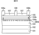
図16は、従来の化合物半導体装置の構造を示す断面図である。SiC基板101上にAlN層102、GaN層103、n型AlGaN104a、n型AlGaN104b及びn型GaN層105が順次形成されている。AlN層102の厚さは150μmである。n型AlGaN層104b及びn型GaN層105の総厚は30nm程度である。更に、n型GaN層105上にSiN層107が形成されている。SiN層107に複数の開口部が形成されており、これらの開口部内にソース電極108a、ドレイン電極108b及びゲート電極109が埋め込まれている。
FIG. 16 is a cross-sectional view showing the structure of a conventional compound semiconductor device. An
但し、この化合物半導体装置はノーマリオンタイプである。化合物半導体装置は自動車部品に用いられることがある。しかし、ノーマリオンタイプでは、交通事故等により故障が生じた際に、自動車部品に電流が流れ続けてしまう。そこで、近時、ノーマリオフタイプの化合物半導体装置の要請が高まっている。 However, this compound semiconductor device is a normally-on type. Compound semiconductor devices are sometimes used for automobile parts. However, in the normally-on type, when a failure occurs due to a traffic accident or the like, current continues to flow through the automobile parts. Therefore, recently, there is an increasing demand for normally-off type compound semiconductor devices.
ノーマリオフタイプの化合物半導体装置を実現するためには、閾値電圧を正にすればよい。そこで、リセスゲート構造が提案されている。しかしながら、リセスゲート構造の化合物半導体装置を精度よく製造することは困難である。これは、化合物半導体装置を構成する各半導体層の加工に好適な選択エッチングが見出されておらず、時間制御のドライエッチングを行っているからである。 In order to realize a normally-off type compound semiconductor device, the threshold voltage may be positive. Therefore, a recess gate structure has been proposed. However, it is difficult to accurately manufacture a compound semiconductor device having a recessed gate structure. This is because selective etching suitable for processing each semiconductor layer constituting the compound semiconductor device has not been found, and time-controlled dry etching is performed.
また、図16に示す従来の化合物半導体装置では、入力電力を大きくしていくと、飽和領域において正のゲートリーク電流が流れる。これは、ゲート電極109とn型GaN層105とが直接接触しているためである。このようなゲートリーク電流が流れると、飽和出力状態で使用し続けることが困難であり、携帯電話の基地局用アンプに好適であるとはいい難い。
In the conventional compound semiconductor device shown in FIG. 16, when the input power is increased, a positive gate leakage current flows in the saturation region. This is because the
そこで、n型GaN層105とゲート電極109との間に絶縁体層が挟みこまれた構造が提案されている。しかしながら、絶縁体層が存在する場合、ゲートリーク電流が低減するものの、閾値電圧が深くなってしまう。このため、この構造では、閾値電圧を正にすることも不可能であると考えられている。更に、ゲートリーク電流が低減しても、耐圧が低下してしまう。これは、絶縁体層とn型GaN層105との間のトラップの影響のためである。
Accordingly, a structure in which an insulator layer is sandwiched between the n-
本発明は、ゲート電圧を0としたときに流れる電流を抑制することができ、かつ、高い再現性で製造することができる化合物半導体装置及びその製造方法を提供することを目的とする。 An object of the present invention is to provide a compound semiconductor device that can suppress a current flowing when a gate voltage is set to 0 and can be manufactured with high reproducibility, and a manufacturing method thereof.
本願発明者は、前記課題を解決すべく鋭意検討を重ねた結果、以下に示す発明の諸態様に想到した。 As a result of intensive studies to solve the above problems, the present inventor has come up with various aspects of the invention described below.
本発明に係る化合物半導体装置では、半導体基板上にGaN系のキャリア走行層が形成され、前記キャリア走行層上にGaN系のキャリア供給層が形成され、前記キャリア供給層上にGaN保護層が形成され、前記保護層上にソース電極、ドレイン電極及びゲート電極が形成されている。また、前記保護層上には、前記ゲート電極と前記ソース電極との間及び前記ゲート電極と前記ドレイン電極との間に位置するAlN又はInAlNの化合物半導体層が形成され、前記化合物半導体層上に絶縁体層が形成されている。 In the compound semiconductor device according to the present invention is formed carrier transit layer GaN system on a semiconductor substrate, said carrier supplying layer of GaN based on the carrier transit layer is formed, Ga N coercive Mamoruso the carrier supply layer A source electrode, a drain electrode, and a gate electrode are formed on the protective layer. Further, an AlN or InAlN compound semiconductor layer located between the gate electrode and the source electrode and between the gate electrode and the drain electrode is formed on the protective layer, and is formed on the compound semiconductor layer. An insulator layer is formed.
本発明に係る化合物半導体装置の製造方法では、半導体基板上にGaN系のキャリア走行層を形成した後、前記キャリア走行層上にGaN系のキャリア供給層を形成する。次に、前記キャリア供給層上にGaN保護層を形成する。次いで、前記保護層上にAlN又はInAlNの化合物半導体層を形成する。その後、前記化合物半導体層上に絶縁体層を形成する。続いて、前記絶縁体層及び前記化合物半導体層に、ソース電極用の開口部、ドレイン電極用の開口部及びゲート電極用の開口部を形成する。そして、前記3個の開口部内に電極を形成する。但し、前記ゲート電極用の開口部を形成する工程では、前記化合物半導体層を前記保護層が露出するまでウェットエッチングする。 In the method for manufacturing a compound semiconductor device according to the present invention, after forming a GaN-based carrier running layer on a semiconductor substrate, a GaN-based carrier supply layer is formed on the carrier running layer. Next, a Ga N coercive Mamoruso the carrier supply layer. Next, an AlN or InAlN compound semiconductor layer is formed on the protective layer. Thereafter, an insulator layer is formed on the compound semiconductor layer. Subsequently, an opening for a source electrode, an opening for a drain electrode, and an opening for a gate electrode are formed in the insulator layer and the compound semiconductor layer. Then, electrodes are formed in the three openings. However, in the step of forming the opening for the gate electrode, the compound semiconductor layer is wet-etched until the protective layer is exposed.
以下、本発明の実施形態について添付の図面を参照して具体的に説明する。 Hereinafter, embodiments of the present invention will be specifically described with reference to the accompanying drawings.
(第1の実施形態)
先ず、本発明の第1の実施形態について説明する。図1は、本発明の第1の実施形態に係る化合物半導体装置の構造を示す断面図である。(First embodiment)
First, a first embodiment of the present invention will be described. FIG. 1 is a sectional view showing the structure of a compound semiconductor device according to the first embodiment of the present invention.
第1の実施形態では、SiC基板1上に、厚さが150nm乃至300nm程度のAlN層2が形成されている。AlN層2上に、厚さが3μm程度のGaNバッファ層3(キャリア走行層)が形成されている。GaNバッファ層3上に、厚さが5nm程度のノンドープAlGaN層4aが形成されている。ノンドープAlGaN層4a上に、厚さが15nm乃至20nm程度のn型AlGaN層4b(キャリア供給層)が形成されている。n型AlGaN層4bには、Siが4×1018cm−3程度ドーピングされている。更に、n型AlGaN層4b上に、厚さが7nm程度のn型GaN層5(保護層)が形成されている。n型GaN層5には、Siが5×1018cm−3程度ドーピングされている。n型GaN層5上に、厚さが3nm程度のノンドープAlN層6及び厚さが20nm程度のSiN層7が順次形成されている。ノンドープAlN層6とSiN層7との間には、半導体−絶縁体接合がある。ノンドープAlN層6及びSiN層7には、少なくとも3個の開口部(ソース電極用、ドレイン電極用及びゲート電極用)が形成されており、これらの開口部内に、ソース電極8a、ドレイン電極8b及びゲート電極19が埋め込まれている。ノンドープAlN層6とゲート電極19との間には、半導体−金属接合がある。また、ゲート電極19とn型GaN層5との間には、金属−半導体接合がある。ソース電極8a及びドレイン電極8bは、例えば、厚さが10nm程度のTa膜とその上に形成された厚さが300nm程度のAl膜とから構成されている。また、ゲート電極19は、例えばNi膜とその上に形成されたAu膜とから構成されている。In the first embodiment, an
このような第1の実施形態では、ノンドープAlGaN層4aのGaNバッファ層3との界面近傍に、格子不整合に起因するピエゾ効果が生じる。このため、正の分極電荷が現れ、GaNバッファ層3のノンドープAlGaN層4aとの界面近傍に電子が誘起される。この結果、2次元電子ガス層(2DEG)が現れる。
In such a first embodiment, a piezo effect due to lattice mismatch occurs near the interface between the
また、ゲート電極19の周囲に絶縁体層としてSiN層7が存在するため、側面からのゲートリーク電流を防止することができる。従って、高耐圧化が可能となる。
In addition, since the
更に、SiN層7とn型GaN層5との間にノンドープAlN層6が存在するため、ノンドープAlN層6とn型GaN層5との界面に電子が存在する。従って、ゲート電極19とソース電極8a及びドレイン電極8bとの間の電子走行領域に2次元電子ガスが多く存在する。従って、相互コンダクタンス(Gm)が向上し、オン抵抗が低く抑えられる。また、ゲートリセス構造の採用により、閾値電圧がより0Vに近くなる。つまり、これらの相互作用により、閾値電圧を0Vに近づけながら十分な電流を確保することが可能となる。
Furthermore, since the
次に、第1の実施形態に係る化合物半導体装置を製造する方法について説明する。図2A乃至図2Gは、本発明の第1の実施形態に係る化合物半導体装置の製造方法を工程順に示す断面図である。 Next, a method for manufacturing the compound semiconductor device according to the first embodiment will be described. 2A to 2G are cross-sectional views showing a method of manufacturing the compound semiconductor device according to the first embodiment of the present invention in the order of steps.
先ず、図2Aに示すように、SiC基板1上にAlN層2を形成する。次に、AlN層2上にGaNバッファ層3を形成する。次いで、GaNバッファ層3上にノンドープAlGaN層4aを形成する。その後、ノンドープAlGaN層4a上にn型AlGaN層4bを形成する。続いて、n型AlGaN層4b上にn型GaN層5を形成する。次に、n型GaN層5上にノンドープAlN層6を形成する。次いで、ノンドープAlN層6上にSiN層7を形成する。AlN層2、GaNバッファ層3、ノンドープAlGaN層4a、n型AlGaN層4b、n型GaN層5及びノンドープAlN層6の形成は、例えばMOCVD法等の結晶成長法により行う。また、SiN層7の形成は、例えばプラズマCVD法により行う。
First, as shown in FIG. 2A, an
次に、図2Bに示すように、SiN層7上に、ソース電極8a及びドレイン電極8bを形成する予定の領域に開口部が存在するレジストパターン21を形成する。
Next, as shown in FIG. 2B, a resist
次いで、図2Cに示すように、レジストパターン21をマスクとして用いて、SiN層7及びノンドープAlN層6のウェットエッチングを行うことにより、SiN層7及びノンドープAlN層6に、ソース電極用の開口部及びドレイン電極用の開口部を形成する。このとき、ノンドープAlN層6の下に位置するn型GaN層5はウェットエッチングでは除去されないため、n型GaN層5の表面においてエッチングが停止する。開口部の形成後に、レジストパターン21を除去する。
Next, as shown in FIG. 2C, by performing wet etching of the
その後、図2Dに示すように、SiN層7及びノンドープAlN層6の開口部内にソース電極8a及びドレイン電極8bを形成する。
Thereafter, as shown in FIG. 2D, a
続いて、図2Eに示すように、SiN層7、ソース電極8a及びドレイン電極8b上に、ゲート電極19を形成する予定の領域に開口部が存在するレジストパターン22を形成する。
Subsequently, as shown in FIG. 2E, a resist
次に、図2Fに示すように、レジストパターン22をマスクとして用いて、SiN層7及びノンドープAlN層6のウェットエッチング(酸を用いたエッチング)を行うことにより、SiN層7及びノンドープAlN層6に、ゲート電極用の開口部を形成する。このときも、ノンドープAlN層6の下に位置するn型GaN層5はウェットエッチングでは除去されないため、n型GaN層5の表面においてエッチングが停止する。開口部の形成後に、レジストパターン22を除去する。
Next, as shown in FIG. 2F, the
次いで、図2Gに示すように、SiN層7及びノンドープAlN層6の開口部内にゲート電極19(埋め込み型ゲート電極)を形成する。なお、図示していないが、素子分離は、例えばイオン注入により行うことができる。
Next, as shown in FIG. 2G, a gate electrode 19 (buried gate electrode) is formed in the openings of the
このような製造方法によれば、ノンドープAlN層6とn型GaN層5とのウェットエッチング時の選択比が高いため、ノンドープAlN層6を高い精度で加工することができる。従って、再現性のよいゲート電極19を高い精度で形成することができる。
According to such a manufacturing method, since the selectivity at the time of wet etching between the
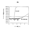
ここで、本願発明者が上述の方法に従って製造した化合物半導体装置のデバイス特性について説明する。図3は、本願発明者が測定した第1の実施形態に係る化合物半導体装置のデバイス特性を示すグラフである。図3には、参考のために、図16に示す従来の化合物半導体装置のデバイス特性も示す。横軸はゲート−ソース間電圧(Vgs)であり、縦軸は相互コンダクタンス(Gm)である。図3に示すように、従来の化合物半導体装置と比較すると、第1の実施形態では閾値電圧がより0Vに近づいた。 Here, the device characteristics of the compound semiconductor device manufactured by the present inventor according to the above-described method will be described. FIG. 3 is a graph showing device characteristics of the compound semiconductor device according to the first embodiment measured by the inventor of the present application. FIG. 3 also shows device characteristics of the conventional compound semiconductor device shown in FIG. 16 for reference. The horizontal axis is the gate-source voltage (Vgs), and the vertical axis is the mutual conductance (Gm). As shown in FIG. 3, the threshold voltage is closer to 0 V in the first embodiment as compared with the conventional compound semiconductor device.
なお、第1の実施形態では、ソース電極8a及びドレイン電極8bの底面がn型GaN層5の表面と接しているが、図15に示すように、n型AlGaN層4bの表面に接するようにしてもよい。この場合には、例えば、図2Bに示すレジストパターン21をマスクとして用いてSiN層7及びノンドープAlN層6に、ソース電極用の開口部及びドレイン電極用の開口部を形成した後、レジストパターン21を残したまま、n型GaN層5のドライエッチングを行う。このドライエッチングでは、例えば、圧力を2Paとし、Cl2流量を10sccmとし、エッチング速度を10nm/分として、反応性イオンエッチング(RIE)を行う。ドライエッチングの終点は、例えば時間制御により決定する。なお、エッチング量の誤差は±3nm以内とすることが好ましい。この場合にも、ソース電極8a及び8bは、例えば、厚さが10nm程度のTa膜とその上に形成された厚さが300nm程度のAl膜とから構成される。このような電極及びその周辺の構造は、以下の実施形態にも適用することができる。In the first embodiment, the bottom surfaces of the
(第2の実施形態)
次に、本発明の第2の実施形態について説明する。図4は、本発明の第2の実施形態に係る化合物半導体装置の構造を示す断面図である。(Second Embodiment)
Next, a second embodiment of the present invention will be described. FIG. 4 is a sectional view showing the structure of a compound semiconductor device according to the second embodiment of the present invention.
第2の実施形態では、ノンドープAlN層6のゲート電極用の開口部の大きさは第1の実施形態のそれと同程度であるのに対し、SiN層7のゲート電極用の開口部が第1の実施形態のそれよりも広い。そして、この開口部に、オーバーハング部を備えたゲート電極29が埋め込まれている。他の構成は、第1の実施形態と同様である。
In the second embodiment, the size of the opening for the gate electrode of the
このような第2の実施形態によれば、ゲート電極29とノンドープAlN層6との界面近傍における電界集中が、第1の実施形態におけるゲート電極19とノンドープAlN層6との界面近傍における電界集中よりも緩和される。化合物半導体装置のゲートとドレインとの間には50V乃至500Vの電圧が印加されることがあるが、第2の実施形態によれば、このような場合でも、劣化がより一層生じにくくなる。
According to the second embodiment, the electric field concentration in the vicinity of the interface between the
次に、第2の実施形態に係る化合物半導体装置を製造する方法について説明する。図5A乃至図5Cは、本発明の第2の実施形態に係る化合物半導体装置の製造方法を工程順に示す断面図である。 Next, a method for manufacturing the compound semiconductor device according to the second embodiment will be described. 5A to 5C are cross-sectional views showing a method of manufacturing a compound semiconductor device according to the second embodiment of the present invention in the order of steps.
先ず、第1の実施形態の場合と同様にして、レジストパターン22の除去(図2F参照)までの処理を行う。次に、図5Aに示すように、SiN層7、ソース電極8a及びドレイン電極8b上に、ゲート電極29のオーバーハング部を形成する予定の領域に開口部が存在するレジストパターン23を形成する。
First, processing up to the removal of the resist pattern 22 (see FIG. 2F) is performed in the same manner as in the first embodiment. Next, as shown in FIG. 5A, a resist
次に、図5Bに示すように、レジストパターン23をマスクとして用いて、SiN層7のウェットエッチングを行うことにより、SiN層7に、オーバーハング部用の開口部を形成する。開口部の形成後に、レジストパターン23を除去する。
Next, as shown in FIG. 5B, the
次いで、図5Cに示すように、SiN層7及びノンドープAlN層6の開口部内にゲート電極29(埋め込み型ゲート電極)を形成する。なお、図示していないが、素子分離は、例えばイオン注入により行うことができる。
Next, as shown in FIG. 5C, a gate electrode 29 (buried gate electrode) is formed in the openings of the
ここで、本願発明者が上述の方法に従って製造した化合物半導体装置のデバイス特性について説明する。図6は、本願発明者が測定した第2の実施形態に係る化合物半導体装置のデバイス特性を示すグラフである。図6には、参考のために、図16に示す従来の化合物半導体装置のデバイス特性も示す。横軸はゲート−ドレイン間電圧(Vgd)であり、縦軸はゲート−ドレイン間電流(Igd)である。図6に示すように、従来の化合物半導体装置と比較すると、第2の実施形態では、逆方向ゲートリーク電流が低減した。更に、飽和電流が減少することなく、閾値電圧が0Vに近づいた。 Here, the device characteristics of the compound semiconductor device manufactured by the present inventor according to the above-described method will be described. FIG. 6 is a graph showing device characteristics of the compound semiconductor device according to the second embodiment measured by the inventor of the present application. FIG. 6 also shows device characteristics of the conventional compound semiconductor device shown in FIG. 16 for reference. The horizontal axis is the gate-drain voltage (Vgd), and the vertical axis is the gate-drain current (Igd). As shown in FIG. 6, compared to the conventional compound semiconductor device, the reverse gate leakage current is reduced in the second embodiment. Furthermore, the threshold voltage approached 0V without decreasing the saturation current.
(第3の実施形態)
次に、本発明の第3の実施形態について説明する。第3の実施形態では、MIS(Metal-Insulator-Semiconductor)構造が採用されている。図7は、本発明の第3の実施形態に係る化合物半導体装置の構造を示す断面図である。(Third embodiment)
Next, a third embodiment of the present invention will be described. In the third embodiment, a MIS (Metal-Insulator-Semiconductor) structure is employed. FIG. 7 is a sectional view showing the structure of a compound semiconductor device according to the third embodiment of the present invention.
第3の実施形態では、ノンドープAlN層6の上に、厚さが10nm程度のSiN層7aが形成されている。ノンドープAlN層6及びSiN層7aには、少なくとも3個の開口部(ソース電極用、ドレイン電極用及びゲート電極用)が形成されている。本実施形態では、3個の開口部のうちのゲート電極用の開口部内及びSiN層7a上に、厚さが10nm程度のSiN層7bが形成されている。そして、ゲート電極用の開口部内に、オーバーハング部を備えたゲート電極39が埋め込まれている。他の構成は、第1の実施形態と同様である。
In the third embodiment, a
このような第3の実施形態によれば、順方向ゲートリーク電流を大幅に低減することができる。また、完全なノーマリオフ動作を行うことができる。また、ノーマリオフ動作の実現により、高い電流を得ることも可能となる。 According to the third embodiment, forward gate leakage current can be greatly reduced. In addition, a complete normally-off operation can be performed. In addition, a high current can be obtained by realizing the normally-off operation.
次に、第3の実施形態に係る化合物半導体装置を製造する方法について説明する。図8A乃至図8Eは、本発明の第3の実施形態に係る化合物半導体装置の製造方法を工程順に示す断面図である。 Next, a method for manufacturing the compound semiconductor device according to the third embodiment will be described. 8A to 8E are cross-sectional views showing a method of manufacturing a compound semiconductor device according to the third embodiment of the present invention in the order of steps.
先ず、第1の実施形態と同様にして、ノンドープSiN層6の形成(図2A参照)までの処理を行う。次に、図8Aに示すように、ノンドープSiN層6上にSiN層7aを形成する。SiN層7aの形成は、例えばプラズマCVD法により行う。
First, similarly to the first embodiment, the processes up to the formation of the non-doped SiN layer 6 (see FIG. 2A) are performed. Next, as shown in FIG. 8A, a
次いで、第1の実施形態と同様にして、ソース電極8a及びドレイン電極8bの形成(図2D参照)までの処理を行う。その後、図8Bに示すように、SiN層7a、ソース電極8a及びドレイン電極8b上に、ゲート電極39の下部を形成する予定の領域に開口部が存在するレジストパターン24を形成する。
Next, similarly to the first embodiment, processing up to the formation of the
続いて、図8Cに示すように、レジストパターン24をマスクとして用いて、SiN層7a及びノンドープAlN層6のウェットエッチングを行うことにより、SiN層7a及びノンドープAlN層6に、ゲート電極用の開口部を形成する。このとき、ノンドープAlN層6の下に位置するn型GaN層5はウェットエッチングでは除去されないため、n型GaN層5の表面においてエッチングが停止する。開口部の形成後に、レジストパターン24を除去する。
Subsequently, as shown in FIG. 8C, the
次に、図8Dに示すように、ゲート電極用の開口部内及びSiN層7a上にSiN層7bを形成する。SiN層7bの形成は、例えばプラズマCVD法により行う。
Next, as shown in FIG. 8D, the
次いで、図8Eに示すように、SiN層7a及びノンドープAlN層6の開口部内にゲート電極39(埋め込み型ゲート電極)を形成する。なお、図示していないが、素子分離は、例えばイオン注入により行うことができる。
Next, as shown in FIG. 8E, a gate electrode 39 (buried gate electrode) is formed in the openings of the
ここで、本願発明者が上述の方法に従って製造した化合物半導体装置のデバイス特性について説明する。図9は、本願発明者が測定した第3の実施形態に係る化合物半導体装置のデバイス特性を示すグラフである。図9には、参考のために、図16に示す従来の化合物半導体装置のデバイス特性も示す。横軸はゲート電圧であり、縦軸は順方向ゲートリーク電流である。図9に示すように、従来の化合物半導体装置と比較すると、第3の実施形態では、順方向ゲートリーク電流が低減した。即ち、第3の実施形態では、ゲート電圧を4V程度まで高くしても、ゲートリーク電流はほとんど流れなかった。 Here, the device characteristics of the compound semiconductor device manufactured by the present inventor according to the above-described method will be described. FIG. 9 is a graph showing device characteristics of the compound semiconductor device according to the third embodiment measured by the inventors of the present application. FIG. 9 also shows device characteristics of the conventional compound semiconductor device shown in FIG. 16 for reference. The horizontal axis is the gate voltage, and the vertical axis is the forward gate leakage current. As shown in FIG. 9, compared with the conventional compound semiconductor device, the forward gate leakage current is reduced in the third embodiment. That is, in the third embodiment, even when the gate voltage is increased to about 4V, the gate leakage current hardly flows.
また、表1に、本願発明者が上述の方法に従って製造した化合物半導体装置のデバイス特性(閾値電圧Vth、そのばらつきσVth及び最大電流Imax)を示す。表1には、参考のために、図16に示す従来の化合物半導体装置のデバイス特性も示す。従来の化合物半導体装置では、閾値電圧Vthが負であるのに対し、第3の実施形態では、閾値電圧Vthが正となった。また、閾値電圧のばらつきσVthが、第3の実施形態では、従来の化合物半導体装置の1/10程度となった。これは、第3の実施形態では、ゲート電極39近傍の構造を高い再現性で形成することができるのに対し、従来の化合物半導体装置では再現性が低いためである。更に、第3の実施形態では、ゲートリーク電流の低減に伴って最大電流Imaxが従来の化合物半導体装置と比較して著しく高くなった。Table 1 shows device characteristics (threshold voltage Vth, variation σ Vth and maximum current Imax) of the compound semiconductor device manufactured by the inventor in accordance with the above-described method. Table 1 also shows device characteristics of the conventional compound semiconductor device shown in FIG. 16 for reference. In the conventional compound semiconductor device, the threshold voltage Vth is negative, whereas in the third embodiment, the threshold voltage Vth is positive. In addition, the threshold voltage variation σ Vth is about 1/10 that of the conventional compound semiconductor device in the third embodiment. This is because in the third embodiment, the structure in the vicinity of the

(第4の実施形態)
次に、本発明の第4の実施形態について説明する。図10は、本発明の第4の実施形態に係る化合物半導体装置の構造を示す断面図である。(Fourth embodiment)
Next, a fourth embodiment of the present invention will be described. FIG. 10 is a sectional view showing the structure of a compound semiconductor device according to the fourth embodiment of the present invention.
第4の実施形態では、ノンドープAlN層6とSiN層7aとの間に、厚さが7nm程度のn型GaN層11が形成されている。n型GaN層11には、Siが5×1018cm−3程度ドーピングされている。n型GaN層11には、ノンドープAlN層6及びSiN層7aと同様の開口部が形成されている。他の構成は第3の実施形態と同様である。なお、n型GaN層11のSiのドーピング量がn型GaN層5のそれよりも高くてもよい。In the fourth embodiment, an n-
このような第4の実施形態によれば、ノンドープAlN層6上にn型GaN層11が形成されているため、ノンドープAlN層6の化学的な変化がより生じにくい。このため、装置全体の劣化が生じにくく、高い信頼性が得られる。
According to the fourth embodiment as described above, since the n-
なお、第4の実施形態に係る化合物半導体装置を製造するに当たっては、例えば、ノンドープAlN層6の形成とSiN層7aの形成との間に、n型GaN層11をノンドープAlN層6上に形成する。そして、SiN層7aに開口部を形成した後に、n型GaN層11のドライエッチングを行う。このドライエッチングは、時間制御により行う。次いで、第1乃至第3の実施形態と同様にして、ノンドープAlN層6のウェットエッチングを行う。このとき、ノンドープAlN層6の下に位置するn型GaN層5はウェットエッチングでは除去されないため、n型GaN層5の表面においてエッチングが停止する。
In manufacturing the compound semiconductor device according to the fourth embodiment, for example, the n-
ここで、本願発明者が上述の方法に従って製造した化合物半導体装置の信頼度について説明する。図11は、本願発明者が測定した第4の実施形態に係る化合物半導体装置の信頼度の試験データを示すグラフである。図11には、参考のために、図16に示す従来の化合物半導体装置の試験データ(3種類)も示す。横軸はゲートリーク電流Igであり、縦軸は試験時間である。図11に示すように、従来の化合物半導体装置では、試験開始時においてもゲートリーク電流が高く、また、試料によっては時間の経過につれてゲートリーク電流が増加した。これは、劣化が進行していることを示している。これに対し、第4の実施形態では、試験開始時におけるゲートリーク電流が低く、更に、時間の経過に伴う増加は全く観察されなかった。 Here, the reliability of the compound semiconductor device manufactured by the inventor according to the above-described method will be described. FIG. 11 is a graph showing reliability test data of the compound semiconductor device according to the fourth embodiment measured by the inventor of the present application. FIG. 11 also shows test data (three types) of the conventional compound semiconductor device shown in FIG. 16 for reference. The horizontal axis is the gate leakage current Ig, and the vertical axis is the test time. As shown in FIG. 11, in the conventional compound semiconductor device, the gate leakage current was high even at the start of the test, and the gate leakage current increased over time depending on the sample. This indicates that the deterioration is progressing. On the other hand, in the fourth embodiment, the gate leakage current at the start of the test was low, and no increase with time was observed at all.
(第5の実施形態)
次に、本発明の第5の実施形態について説明する。図12は、本発明の第5の実施形態に係る化合物半導体装置の構造を示す断面図である。(Fifth embodiment)
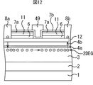
Next, a fifth embodiment of the present invention will be described. FIG. 12 is a sectional view showing the structure of a compound semiconductor device according to the fifth embodiment of the present invention.
第5の実施形態では、第4の実施形態におけるn型GaN層5の代わりにノンドープGaN層12が形成されている。
In the fifth embodiment, a
このような第5の実施形態によれば、n型GaN層5の代わりにノンドープGaN層12が用いられているため、ゲートリーク電流をより一層低減することができる。また、第3の実施形態と同様にMIS構造を採用しているため、ノンドープGaN層12を用いても特性が低下することはない。
According to the fifth embodiment, since the
(第6の実施形態)
次に、本発明の第6の実施形態について説明する。図13は、本発明の第6の実施形態に係る化合物半導体装置の構造を示す断面図である。(Sixth embodiment)
Next, a sixth embodiment of the present invention will be described. FIG. 13 is a sectional view showing the structure of a compound semiconductor device according to the sixth embodiment of the present invention.
第6の実施形態では、第5の実施形態におけるn型GaN層11の代わりにn型InGaN層13が形成されている。
In the sixth embodiment, an n-
このような第6の実施形態によれば、n型GaN層11の代わりにn型InGaN層13が用いられているため、この層でのバンドが下がり、2次元電子ガスが増加する。この結果、最大電流が増加する。
According to the sixth embodiment, since the n-
(第7の実施形態)
次に、本発明の第7の実施形態について説明する。図14は、本発明の第7の実施形態に係る化合物半導体装置の構造を示す断面図である。(Seventh embodiment)
Next, a seventh embodiment of the present invention will be described. FIG. 14 is a sectional view showing the structure of a compound semiconductor device according to the seventh embodiment of the present invention.
第7の実施形態では、第4の実施形態におけるノンドープAlN層6とn型GaN層11との間に、1原子層分のSi層14が形成されている。Si層14は、例えばプレーナドーピング法(原子層ドーピング法)により形成される。
In the seventh embodiment, an
このような第7の実施形態によれば、電極間の抵抗が低下し、最大電流が増加する。なお、Si層14がn型GaN層5とノンドープAlN層6との間に形成されていてもよい。
According to such a seventh embodiment, the resistance between the electrodes decreases, and the maximum current increases. Note that the
なお、AlN層の形成をALD(Atomic Layer Deposition)法又はスパッタリング法等により行ってもよい。この場合、AlN層の結晶方位は、その下のGaN層の影響を受けにくくなる。また、これらの実施形態では、ゲート電極とソース電極及びドレイン電極との間に、Nを含む化合物半導体層としてAlN層が形成されているが、他の化合物半導体層、例えばInAlN等のInを含む層が形成されていてもよい。更に、これらの実施形態では、単体のHEMTについて説明しているが、複数のHEMTを集積してもよい。この場合には、例えばイオン注入又はメサエッチング等によって素子分離を行えばよい。 The AlN layer may be formed by an ALD (Atomic Layer Deposition) method or a sputtering method. In this case, the crystal orientation of the AlN layer is less affected by the underlying GaN layer. In these embodiments, an AlN layer is formed as a compound semiconductor layer containing N between the gate electrode, the source electrode, and the drain electrode, but other compound semiconductor layers, for example, In such as InAlN are included. A layer may be formed. Furthermore, in these embodiments, a single HEMT has been described, but a plurality of HEMTs may be integrated. In this case, element isolation may be performed by, for example, ion implantation or mesa etching.
本発明によれば、保護層上にNを含む化合物半導体層が形成されており、この化合物半導体層の加工を、保護層への影響がない条件下で行うことができる。このため、高い再現性でゲートリセス構造を構築することができる。このため、ゲート電圧を0としたときに流れる電流を抑制することができる。また、絶縁体層がゲート電極の側面に接している場合には、ゲートリーク電流を抑制することができ、高耐圧化することができる。
According to the present invention, the compound semiconductor layer containing N is formed on the protective layer, and this compound semiconductor layer can be processed under conditions that do not affect the protective layer. For this reason, a gate recess structure can be constructed with high reproducibility. For this reason, the current that flows when the gate voltage is 0 can be suppressed. In addition, when the insulator layer is in contact with the side surface of the gate electrode, the gate leakage current can be suppressed and the breakdown voltage can be increased.
Claims (23)
前記キャリア走行層上に形成されたGaN系のキャリア供給層と、
前記キャリア供給層上に形成されたGaN保護層と、
前記保護層上に形成されたソース電極、ドレイン電極及びゲート電極と、
前記保護層上に形成され、前記ゲート電極と前記ソース電極との間及び前記ゲート電極と前記ドレイン電極との間に位置するAlN又はInAlNの化合物半導体層と、
前記化合物半導体層上に形成された絶縁体層と、
を有することを特徴とする化合物半導体装置。A GaN-based carrier running layer formed on a semiconductor substrate;
A GaN-based carrier supply layer formed on the carrier running layer;
A GaN protective layer formed on the carrier supply layer;
A source electrode, a drain electrode and a gate electrode formed on the protective layer;
An AlN or InAlN compound semiconductor layer formed on the protective layer and located between the gate electrode and the source electrode and between the gate electrode and the drain electrode;
An insulator layer formed on the compound semiconductor layer;
A compound semiconductor device comprising:
前記キャリア走行層上にGaN系のキャリア供給層を形成する工程と、
前記キャリア供給層上にGaN保護層を形成する工程と、
前記保護層上にAlN又はInAlNの化合物半導体層を形成する工程と、
前記化合物半導体層上に絶縁体層を形成する工程と、
前記絶縁体層及び前記化合物半導体層に、ソース電極用の開口部、ドレイン電極用の開口部及びゲート電極用の開口部を形成する工程と、
前記3個の開口部内に電極を形成する工程と、
を有し、
前記ゲート電極用の開口部を形成する工程は、前記化合物半導体層を前記保護層が露出するまでウェットエッチングする工程を有することを特徴とする化合物半導体装置の製造方法。Forming a GaN-based carrier running layer on a semiconductor substrate;
Forming a GaN-based carrier supply layer on the carrier running layer;
Forming a GaN protective layer on the carrier supply layer;
Forming an AlN or InAlN compound semiconductor layer on the protective layer;
Forming an insulator layer on the compound semiconductor layer;
Forming a source electrode opening, a drain electrode opening, and a gate electrode opening in the insulator layer and the compound semiconductor layer;
Forming an electrode in the three openings;
Have
The step of forming the opening for the gate electrode includes a step of wet-etching the compound semiconductor layer until the protective layer is exposed.
前記キャリア走行層上方に形成されたGaN系のキャリア供給層と、
前記キャリア供給層上方に形成されたn型GaN保護層と、
前記n型GaN保護層上方に形成されたAlN層と、
前記AlN層上方に形成されたn型GaN層と、
前記n型GaN層上方に形成された絶縁体層と、
前記キャリア供給層上方に形成されたゲート電極、ソース電極及びドレイン電極と、
を備えたことを特徴とする化合物半導体装置。A GaN-based carrier running layer formed above the semiconductor substrate;
A GaN-based carrier supply layer formed above the carrier running layer;
An n-type GaN protective layer formed above the carrier supply layer;
An AlN layer formed above the n-type GaN protective layer;
An n-type GaN layer formed above the AlN layer;
An insulator layer formed above the n-type GaN layer;
A gate electrode, a source electrode and a drain electrode formed above the carrier supply layer;
A compound semiconductor device comprising:
前記ゲート電極は、前記開口内に形成されていることを特徴とする請求項21に記載の化合物半導体装置。An opening formed in the n-type GaN layer and the AlN layer;
The compound semiconductor device according to claim 21, wherein the gate electrode is formed in the opening.
前記ゲート電極は、前記絶縁体層上方に形成されていることを特徴とする請求項22に記載の化合物半導体装置。The insulator layer is formed in the opening;
23. The compound semiconductor device according to claim 22, wherein the gate electrode is formed above the insulator layer.
Applications Claiming Priority (1)
| Application Number | Priority Date | Filing Date | Title |
|---|---|---|---|
| PCT/JP2006/305265 WO2007108055A1 (en) | 2006-03-16 | 2006-03-16 | Compound semiconductor device and process for producing the same |
Publications (2)
| Publication Number | Publication Date |
|---|---|
| JPWO2007108055A1 JPWO2007108055A1 (en) | 2009-07-30 |
| JP5071377B2 true JP5071377B2 (en) | 2012-11-14 |
Family
ID=38522096
Family Applications (1)
| Application Number | Title | Priority Date | Filing Date |
|---|---|---|---|
| JP2008506071A Active JP5071377B2 (en) | 2006-03-16 | 2006-03-16 | Compound semiconductor device and manufacturing method thereof |
Country Status (4)
| Country | Link |
|---|---|
| US (4) | US8344419B2 (en) |
| EP (5) | EP2677544B1 (en) |
| JP (1) | JP5071377B2 (en) |
| WO (1) | WO2007108055A1 (en) |
Families Citing this family (61)
| Publication number | Priority date | Publication date | Assignee | Title |
|---|---|---|---|---|
| JP2008306130A (en) * | 2007-06-11 | 2008-12-18 | Sanken Electric Co Ltd | Field-effect semiconductor device and its manufacturing method |
| US7915643B2 (en) | 2007-09-17 | 2011-03-29 | Transphorm Inc. | Enhancement mode gallium nitride power devices |
| WO2009066434A1 (en) * | 2007-11-19 | 2009-05-28 | Nec Corporation | Field effect transistor and method for manufacturing the same |
| JP5386829B2 (en) * | 2008-01-30 | 2014-01-15 | 富士通株式会社 | Semiconductor device |
| JP5320774B2 (en) * | 2008-03-03 | 2013-10-23 | 三菱電機株式会社 | Semiconductor device |
| US8519438B2 (en) | 2008-04-23 | 2013-08-27 | Transphorm Inc. | Enhancement mode III-N HEMTs |
| US8289065B2 (en) | 2008-09-23 | 2012-10-16 | Transphorm Inc. | Inductive load power switching circuits |
| JP5468768B2 (en) | 2008-12-05 | 2014-04-09 | パナソニック株式会社 | Field effect transistor and manufacturing method thereof |
| US7898004B2 (en) | 2008-12-10 | 2011-03-01 | Transphorm Inc. | Semiconductor heterostructure diodes |
| JP5487613B2 (en) | 2008-12-19 | 2014-05-07 | 富士通株式会社 | Compound semiconductor device and manufacturing method thereof |
| US8742459B2 (en) | 2009-05-14 | 2014-06-03 | Transphorm Inc. | High voltage III-nitride semiconductor devices |
| JP4794655B2 (en) * | 2009-06-09 | 2011-10-19 | シャープ株式会社 | Field effect transistor |
| US8390000B2 (en) | 2009-08-28 | 2013-03-05 | Transphorm Inc. | Semiconductor devices with field plates |
| RU2506487C2 (en) * | 2009-09-18 | 2014-02-10 | Пайолэкс, Инк. | Hose clamp |
| JP2011082216A (en) | 2009-10-02 | 2011-04-21 | Fujitsu Ltd | Compound semiconductor device and method for manufacturing the same |
| US9378965B2 (en) * | 2009-12-10 | 2016-06-28 | Infineon Technologies Americas Corp. | Highly conductive source/drain contacts in III-nitride transistors |
| US8389977B2 (en) | 2009-12-10 | 2013-03-05 | Transphorm Inc. | Reverse side engineered III-nitride devices |
| CN101916773B (en) * | 2010-07-23 | 2012-05-23 | 中国科学院上海技术物理研究所 | Double-channel MOS-HEMT (Metal Oxide Semiconductor-High Electron Mobility Transistor) device and manufacturing method |
| JP5712583B2 (en) | 2010-12-02 | 2015-05-07 | 富士通株式会社 | Compound semiconductor device and manufacturing method thereof |
| JP5724339B2 (en) * | 2010-12-03 | 2015-05-27 | 富士通株式会社 | Compound semiconductor device and manufacturing method thereof |
| US8742460B2 (en) | 2010-12-15 | 2014-06-03 | Transphorm Inc. | Transistors with isolation regions |
| JP5654884B2 (en) * | 2011-01-26 | 2015-01-14 | 株式会社東芝 | Manufacturing method of nitride semiconductor device |
| US8643062B2 (en) | 2011-02-02 | 2014-02-04 | Transphorm Inc. | III-N device structures and methods |
| JP5762049B2 (en) * | 2011-02-28 | 2015-08-12 | ルネサスエレクトロニクス株式会社 | Semiconductor device |
| US8716141B2 (en) | 2011-03-04 | 2014-05-06 | Transphorm Inc. | Electrode configurations for semiconductor devices |
| US8772842B2 (en) | 2011-03-04 | 2014-07-08 | Transphorm, Inc. | Semiconductor diodes with low reverse bias currents |
| GB201112327D0 (en) * | 2011-07-18 | 2011-08-31 | Epigan Nv | Method for growing III-V epitaxial layers |
| US8901604B2 (en) | 2011-09-06 | 2014-12-02 | Transphorm Inc. | Semiconductor devices with guard rings |
| US9257547B2 (en) | 2011-09-13 | 2016-02-09 | Transphorm Inc. | III-N device structures having a non-insulating substrate |
| US8598937B2 (en) | 2011-10-07 | 2013-12-03 | Transphorm Inc. | High power semiconductor electronic components with increased reliability |
| US9165766B2 (en) | 2012-02-03 | 2015-10-20 | Transphorm Inc. | Buffer layer structures suited for III-nitride devices with foreign substrates |
| JP2013206976A (en) * | 2012-03-27 | 2013-10-07 | Fujitsu Ltd | Compound semiconductor device and manufacturing method of the same |
| US9093366B2 (en) | 2012-04-09 | 2015-07-28 | Transphorm Inc. | N-polar III-nitride transistors |
| US8680536B2 (en) * | 2012-05-23 | 2014-03-25 | Hrl Laboratories, Llc | Non-uniform two dimensional electron gas profile in III-Nitride HEMT devices |
| US9379195B2 (en) | 2012-05-23 | 2016-06-28 | Hrl Laboratories, Llc | HEMT GaN device with a non-uniform lateral two dimensional electron gas profile and method of manufacturing the same |
| US10700201B2 (en) | 2012-05-23 | 2020-06-30 | Hrl Laboratories, Llc | HEMT GaN device with a non-uniform lateral two dimensional electron gas profile and method of manufacturing the same |
| US9000484B2 (en) | 2012-05-23 | 2015-04-07 | Hrl Laboratories, Llc | Non-uniform lateral profile of two-dimensional electron gas charge density in type III nitride HEMT devices using ion implantation through gray scale mask |
| US9184275B2 (en) | 2012-06-27 | 2015-11-10 | Transphorm Inc. | Semiconductor devices with integrated hole collectors |
| US8803246B2 (en) | 2012-07-16 | 2014-08-12 | Transphorm Inc. | Semiconductor electronic components with integrated current limiters |
| JP6087552B2 (en) | 2012-09-21 | 2017-03-01 | トランスフォーム・ジャパン株式会社 | Compound semiconductor device and manufacturing method thereof |
| US9583574B2 (en) | 2012-09-28 | 2017-02-28 | Intel Corporation | Epitaxial buffer layers for group III-N transistors on silicon substrates |
| US8884334B2 (en) * | 2012-11-09 | 2014-11-11 | Taiwan Semiconductor Manufacturing Co., Ltd. | Composite layer stacking for enhancement mode transistor |
| JP2014130951A (en) * | 2012-12-28 | 2014-07-10 | Sumitomo Electric Ind Ltd | Semiconductor device |
| JP6253886B2 (en) * | 2013-01-09 | 2017-12-27 | トランスフォーム・ジャパン株式会社 | Semiconductor device and manufacturing method of semiconductor device |
| CN105164811B (en) | 2013-02-15 | 2018-08-31 | 创世舫电子有限公司 | Electrode of semiconductor devices and forming method thereof |
| US9087718B2 (en) | 2013-03-13 | 2015-07-21 | Transphorm Inc. | Enhancement-mode III-nitride devices |
| US9245993B2 (en) | 2013-03-15 | 2016-01-26 | Transphorm Inc. | Carbon doping semiconductor devices |
| JP5721782B2 (en) * | 2013-06-26 | 2015-05-20 | パナソニック株式会社 | Semiconductor device |
| US9443938B2 (en) | 2013-07-19 | 2016-09-13 | Transphorm Inc. | III-nitride transistor including a p-type depleting layer |
| KR20150011238A (en) * | 2013-07-22 | 2015-01-30 | 삼성전자주식회사 | Nitride-based semiconductor devices |
| JP6214978B2 (en) * | 2013-09-17 | 2017-10-18 | 株式会社東芝 | Semiconductor device |
| US10276712B2 (en) | 2014-05-29 | 2019-04-30 | Hrl Laboratories, Llc | III-nitride field-effect transistor with dual gates |
| US9318593B2 (en) | 2014-07-21 | 2016-04-19 | Transphorm Inc. | Forming enhancement mode III-nitride devices |
| US9536966B2 (en) | 2014-12-16 | 2017-01-03 | Transphorm Inc. | Gate structures for III-N devices |
| US9536967B2 (en) | 2014-12-16 | 2017-01-03 | Transphorm Inc. | Recessed ohmic contacts in a III-N device |
| US9812532B1 (en) | 2015-08-28 | 2017-11-07 | Hrl Laboratories, Llc | III-nitride P-channel transistor |
| ITUB20155503A1 (en) | 2015-11-12 | 2017-05-12 | St Microelectronics Srl | METHOD OF MANUFACTURE OF A HEMT TRANSISTOR AND HEMT TRANSISTOR WITH IMPROVED ELECTRONIC MOBILITY |
| EP3378097A4 (en) | 2015-11-19 | 2019-09-11 | HRL Laboratories, LLC | Iii-nitride field-effect transistor with dual gates |
| WO2017123999A1 (en) | 2016-01-15 | 2017-07-20 | Transphorm Inc. | Enhancement mode iii-nitride devices having an al(1-x)sixo gate insulator |
| TWI762486B (en) | 2016-05-31 | 2022-05-01 | 美商創世舫科技有限公司 | Iii-nitride devices including a graded depleting layer |
| CN112242441A (en) * | 2019-07-16 | 2021-01-19 | 联华电子股份有限公司 | High electron mobility transistor |
Citations (1)
| Publication number | Priority date | Publication date | Assignee | Title |
|---|---|---|---|---|
| JP2002141499A (en) * | 2000-10-31 | 2002-05-17 | Toshiba Corp | Field effect transistor and manufacturing method thereof |
Family Cites Families (9)
| Publication number | Priority date | Publication date | Assignee | Title |
|---|---|---|---|---|
| US5888872A (en) | 1997-06-20 | 1999-03-30 | Advanced Micro Devices, Inc. | Method for forming source drain junction areas self-aligned between a sidewall spacer and an etched lateral sidewall |
| US5986209A (en) | 1997-07-09 | 1999-11-16 | Micron Technology, Inc. | Package stack via bottom leaded plastic (BLP) packaging |
| JP4224737B2 (en) * | 1999-03-04 | 2009-02-18 | ソニー株式会社 | Semiconductor element |
| JP4663156B2 (en) | 2001-05-31 | 2011-03-30 | 富士通株式会社 | Compound semiconductor device |
| WO2003032397A2 (en) * | 2001-07-24 | 2003-04-17 | Cree, Inc. | INSULTING GATE AlGaN/GaN HEMT |
| JP3940699B2 (en) | 2003-05-16 | 2007-07-04 | 株式会社東芝 | Power semiconductor device |
| US7859014B2 (en) * | 2004-06-24 | 2010-12-28 | Nec Corporation | Semiconductor device |
| JP2006032552A (en) * | 2004-07-14 | 2006-02-02 | Toshiba Corp | Semiconductor device containing nitride |
| US7238560B2 (en) * | 2004-07-23 | 2007-07-03 | Cree, Inc. | Methods of fabricating nitride-based transistors with a cap layer and a recessed gate |
-
2006
- 2006-03-16 JP JP2008506071A patent/JP5071377B2/en active Active
- 2006-03-16 WO PCT/JP2006/305265 patent/WO2007108055A1/en active Application Filing
- 2006-03-16 EP EP20130164120 patent/EP2677544B1/en active Active
- 2006-03-16 EP EP06729258A patent/EP1998376B1/en active Active
- 2006-03-16 EP EP09178271A patent/EP2166575B1/en active Active
- 2006-03-16 EP EP13164123.5A patent/EP2657976B1/en active Active
- 2006-03-16 EP EP09178269.8A patent/EP2175494B1/en active Active
-
2008
- 2008-09-15 US US12/210,442 patent/US8344419B2/en active Active
-
2011
- 2011-07-19 US US13/185,946 patent/US8466029B2/en active Active
- 2011-07-19 US US13/185,888 patent/US8637903B2/en active Active
-
2013
- 2013-05-09 US US13/890,688 patent/US8841706B2/en active Active
Patent Citations (1)
| Publication number | Priority date | Publication date | Assignee | Title |
|---|---|---|---|---|
| JP2002141499A (en) * | 2000-10-31 | 2002-05-17 | Toshiba Corp | Field effect transistor and manufacturing method thereof |
Also Published As
| Publication number | Publication date |
|---|---|
| JPWO2007108055A1 (en) | 2009-07-30 |
| EP2175494A3 (en) | 2012-10-17 |
| EP1998376B1 (en) | 2011-08-03 |
| EP2175494B1 (en) | 2015-03-25 |
| US8466029B2 (en) | 2013-06-18 |
| EP2175494A2 (en) | 2010-04-14 |
| WO2007108055A1 (en) | 2007-09-27 |
| US8637903B2 (en) | 2014-01-28 |
| US20090008677A1 (en) | 2009-01-08 |
| EP2166575B1 (en) | 2011-08-17 |
| US8344419B2 (en) | 2013-01-01 |
| EP2657976A2 (en) | 2013-10-30 |
| EP2677544B1 (en) | 2015-04-22 |
| EP2166575A1 (en) | 2010-03-24 |
| EP1998376A4 (en) | 2009-07-22 |
| EP2657976B1 (en) | 2018-12-26 |
| US8841706B2 (en) | 2014-09-23 |
| US20110272704A1 (en) | 2011-11-10 |
| EP2677544A1 (en) | 2013-12-25 |
| EP1998376A1 (en) | 2008-12-03 |
| US20130248934A1 (en) | 2013-09-26 |
| US20110275199A1 (en) | 2011-11-10 |
| EP2657976A3 (en) | 2013-12-25 |
Similar Documents
| Publication | Publication Date | Title |
|---|---|---|
| JP5071377B2 (en) | Compound semiconductor device and manufacturing method thereof | |
| JP6486828B2 (en) | Etching technology for semiconductor structure and recess formation | |
| EP2735031B1 (en) | Method for growing iii-v epitaxial layers | |
| JP5785153B2 (en) | Compensated gate MISFET and manufacturing method thereof | |
| TWI496284B (en) | Compound semiconductor device and method of manufacturing the same | |
| JP5866766B2 (en) | Compound semiconductor device and manufacturing method thereof | |
| JP2008112868A (en) | Semiconductor device, and its manufacturing method | |
| US20180033631A1 (en) | Self-aligning source, drain and gate process for iii-v nitride mishemts | |
| US10243049B2 (en) | Nitride semiconductor device | |
| JP2020523781A (en) | Enhancement-mode GaN transistor using selective and non-selective etching layers to improve GaN spacer thickness uniformity | |
| TW201419530A (en) | Compound semiconductor device and method of manufacturing the same | |
| TWI509797B (en) | Compound semiconductor device and method for manufacturing the same | |
| JP5183975B2 (en) | Enhanced mode field effect device and manufacturing method thereof | |
| US10373833B2 (en) | Semiconductor device and method for manufacturing the same | |
| JP7308593B2 (en) | Nitride semiconductor device | |
| KR20190112523A (en) | Heterostructure Field Effect Transistor and production method thereof | |
| JP2013125918A (en) | Semiconductor device | |
| JP2021086965A (en) | Diode, manufacturing method for diode, and electrical apparatus | |
| JP6047998B2 (en) | Semiconductor device | |
| JP2012033578A (en) | Semiconductor device, and method of manufacturing the same | |
| US20140217416A1 (en) | Nitrides based semiconductor device |
Legal Events
| Date | Code | Title | Description |
|---|---|---|---|
| A521 | Request for written amendment filed |
Free format text: JAPANESE INTERMEDIATE CODE: A523 Effective date: 20091027 |
|
| A131 | Notification of reasons for refusal |
Free format text: JAPANESE INTERMEDIATE CODE: A131 Effective date: 20120207 |
|
| A521 | Request for written amendment filed |
Free format text: JAPANESE INTERMEDIATE CODE: A523 Effective date: 20120405 |
|
| A131 | Notification of reasons for refusal |
Free format text: JAPANESE INTERMEDIATE CODE: A131 Effective date: 20120501 |
|
| A521 | Request for written amendment filed |
Free format text: JAPANESE INTERMEDIATE CODE: A523 Effective date: 20120628 |
|
| TRDD | Decision of grant or rejection written | ||
| A01 | Written decision to grant a patent or to grant a registration (utility model) |
Free format text: JAPANESE INTERMEDIATE CODE: A01 Effective date: 20120724 |
|
| A01 | Written decision to grant a patent or to grant a registration (utility model) |
Free format text: JAPANESE INTERMEDIATE CODE: A01 |
|
| A61 | First payment of annual fees (during grant procedure) |
Free format text: JAPANESE INTERMEDIATE CODE: A61 Effective date: 20120806 |
|
| R150 | Certificate of patent or registration of utility model |
Ref document number: 5071377 Country of ref document: JP Free format text: JAPANESE INTERMEDIATE CODE: R150 Free format text: JAPANESE INTERMEDIATE CODE: R150 |
|
| FPAY | Renewal fee payment (event date is renewal date of database) |
Free format text: PAYMENT UNTIL: 20150831 Year of fee payment: 3 |