EP1998376A1 - Compound semiconductor device and process for producing the same - Google Patents
Compound semiconductor device and process for producing the same Download PDFInfo
- Publication number
- EP1998376A1 EP1998376A1 EP06729258A EP06729258A EP1998376A1 EP 1998376 A1 EP1998376 A1 EP 1998376A1 EP 06729258 A EP06729258 A EP 06729258A EP 06729258 A EP06729258 A EP 06729258A EP 1998376 A1 EP1998376 A1 EP 1998376A1
- Authority
- EP
- European Patent Office
- Prior art keywords
- layer
- compound semiconductor
- semiconductor device
- gate electrode
- forming
- Prior art date
- Legal status (The legal status is an assumption and is not a legal conclusion. Google has not performed a legal analysis and makes no representation as to the accuracy of the status listed.)
- Granted
Links
- 239000004065 semiconductor Substances 0.000 title claims description 142
- 150000001875 compounds Chemical class 0.000 title claims description 135
- 238000000034 method Methods 0.000 title description 18
- 230000008569 process Effects 0.000 title description 9
- 239000000758 substrate Substances 0.000 claims abstract description 9
- 239000010410 layer Substances 0.000 claims description 255
- 238000004519 manufacturing process Methods 0.000 claims description 34
- 239000012212 insulator Substances 0.000 claims description 19
- 239000011241 protective layer Substances 0.000 claims description 19
- 238000001039 wet etching Methods 0.000 claims description 12
- IJGRMHOSHXDMSA-UHFFFAOYSA-N Atomic nitrogen Chemical compound N#N IJGRMHOSHXDMSA-UHFFFAOYSA-N 0.000 claims description 8
- 229910052757 nitrogen Inorganic materials 0.000 claims description 4
- XUIMIQQOPSSXEZ-UHFFFAOYSA-N Silicon Chemical compound [Si] XUIMIQQOPSSXEZ-UHFFFAOYSA-N 0.000 claims 4
- 229910052710 silicon Inorganic materials 0.000 claims 4
- 239000010703 silicon Substances 0.000 claims 4
- 229910052738 indium Inorganic materials 0.000 claims 2
- APFVFJFRJDLVQX-UHFFFAOYSA-N indium atom Chemical compound [In] APFVFJFRJDLVQX-UHFFFAOYSA-N 0.000 claims 2
- 229910002704 AlGaN Inorganic materials 0.000 abstract description 21
- 230000015572 biosynthetic process Effects 0.000 description 9
- 238000005530 etching Methods 0.000 description 9
- 238000005755 formation reaction Methods 0.000 description 9
- 238000001312 dry etching Methods 0.000 description 6
- 238000012360 testing method Methods 0.000 description 6
- 230000007423 decrease Effects 0.000 description 5
- 238000005468 ion implantation Methods 0.000 description 4
- 238000002955 isolation Methods 0.000 description 4
- 230000006866 deterioration Effects 0.000 description 3
- 238000005268 plasma chemical vapour deposition Methods 0.000 description 3
- 230000005533 two-dimensional electron gas Effects 0.000 description 3
- 238000000231 atomic layer deposition Methods 0.000 description 2
- 230000001413 cellular effect Effects 0.000 description 2
- 230000008859 change Effects 0.000 description 2
- 230000005684 electric field Effects 0.000 description 2
- 238000001020 plasma etching Methods 0.000 description 2
- 229910001218 Gallium arsenide Inorganic materials 0.000 description 1
- 206010039203 Road traffic accident Diseases 0.000 description 1
- 239000002253 acid Substances 0.000 description 1
- 239000013078 crystal Substances 0.000 description 1
- 238000002109 crystal growth method Methods 0.000 description 1
- 230000003247 decreasing effect Effects 0.000 description 1
- 238000011161 development Methods 0.000 description 1
- 230000000694 effects Effects 0.000 description 1
- 230000003993 interaction Effects 0.000 description 1
- 239000002184 metal Substances 0.000 description 1
- 238000002488 metal-organic chemical vapour deposition Methods 0.000 description 1
- 230000004048 modification Effects 0.000 description 1
- 238000012986 modification Methods 0.000 description 1
- 230000010287 polarization Effects 0.000 description 1
- 238000012545 processing Methods 0.000 description 1
- 230000001681 protective effect Effects 0.000 description 1
- 230000009467 reduction Effects 0.000 description 1
- 229910052594 sapphire Inorganic materials 0.000 description 1
- 239000010980 sapphire Substances 0.000 description 1
- 238000004544 sputter deposition Methods 0.000 description 1
- 239000000126 substance Substances 0.000 description 1
Images


Classifications
-
- H—ELECTRICITY
- H01—ELECTRIC ELEMENTS
- H01L—SEMICONDUCTOR DEVICES NOT COVERED BY CLASS H10
- H01L29/00—Semiconductor devices adapted for rectifying, amplifying, oscillating or switching, or capacitors or resistors with at least one potential-jump barrier or surface barrier, e.g. PN junction depletion layer or carrier concentration layer; Details of semiconductor bodies or of electrodes thereof ; Multistep manufacturing processes therefor
- H01L29/66—Types of semiconductor device ; Multistep manufacturing processes therefor
- H01L29/68—Types of semiconductor device ; Multistep manufacturing processes therefor controllable by only the electric current supplied, or only the electric potential applied, to an electrode which does not carry the current to be rectified, amplified or switched
- H01L29/76—Unipolar devices, e.g. field effect transistors
- H01L29/772—Field effect transistors
- H01L29/778—Field effect transistors with two-dimensional charge carrier gas channel, e.g. HEMT ; with two-dimensional charge-carrier layer formed at a heterojunction interface
-
- H—ELECTRICITY
- H01—ELECTRIC ELEMENTS
- H01L—SEMICONDUCTOR DEVICES NOT COVERED BY CLASS H10
- H01L29/00—Semiconductor devices adapted for rectifying, amplifying, oscillating or switching, or capacitors or resistors with at least one potential-jump barrier or surface barrier, e.g. PN junction depletion layer or carrier concentration layer; Details of semiconductor bodies or of electrodes thereof ; Multistep manufacturing processes therefor
- H01L29/02—Semiconductor bodies ; Multistep manufacturing processes therefor
- H01L29/12—Semiconductor bodies ; Multistep manufacturing processes therefor characterised by the materials of which they are formed
- H01L29/20—Semiconductor bodies ; Multistep manufacturing processes therefor characterised by the materials of which they are formed including, apart from doping materials or other impurities, only AIIIBV compounds
- H01L29/201—Semiconductor bodies ; Multistep manufacturing processes therefor characterised by the materials of which they are formed including, apart from doping materials or other impurities, only AIIIBV compounds including two or more compounds, e.g. alloys
- H01L29/205—Semiconductor bodies ; Multistep manufacturing processes therefor characterised by the materials of which they are formed including, apart from doping materials or other impurities, only AIIIBV compounds including two or more compounds, e.g. alloys in different semiconductor regions, e.g. heterojunctions
-
- H—ELECTRICITY
- H01—ELECTRIC ELEMENTS
- H01L—SEMICONDUCTOR DEVICES NOT COVERED BY CLASS H10
- H01L29/00—Semiconductor devices adapted for rectifying, amplifying, oscillating or switching, or capacitors or resistors with at least one potential-jump barrier or surface barrier, e.g. PN junction depletion layer or carrier concentration layer; Details of semiconductor bodies or of electrodes thereof ; Multistep manufacturing processes therefor
- H01L29/02—Semiconductor bodies ; Multistep manufacturing processes therefor
- H01L29/12—Semiconductor bodies ; Multistep manufacturing processes therefor characterised by the materials of which they are formed
- H01L29/26—Semiconductor bodies ; Multistep manufacturing processes therefor characterised by the materials of which they are formed including, apart from doping materials or other impurities, elements provided for in two or more of the groups H01L29/16, H01L29/18, H01L29/20, H01L29/22, H01L29/24, e.g. alloys
- H01L29/267—Semiconductor bodies ; Multistep manufacturing processes therefor characterised by the materials of which they are formed including, apart from doping materials or other impurities, elements provided for in two or more of the groups H01L29/16, H01L29/18, H01L29/20, H01L29/22, H01L29/24, e.g. alloys in different semiconductor regions, e.g. heterojunctions
-
- H—ELECTRICITY
- H01—ELECTRIC ELEMENTS
- H01L—SEMICONDUCTOR DEVICES NOT COVERED BY CLASS H10
- H01L29/00—Semiconductor devices adapted for rectifying, amplifying, oscillating or switching, or capacitors or resistors with at least one potential-jump barrier or surface barrier, e.g. PN junction depletion layer or carrier concentration layer; Details of semiconductor bodies or of electrodes thereof ; Multistep manufacturing processes therefor
- H01L29/66—Types of semiconductor device ; Multistep manufacturing processes therefor
- H01L29/66007—Multistep manufacturing processes
- H01L29/66075—Multistep manufacturing processes of devices having semiconductor bodies comprising group 14 or group 13/15 materials
- H01L29/66227—Multistep manufacturing processes of devices having semiconductor bodies comprising group 14 or group 13/15 materials the devices being controllable only by the electric current supplied or the electric potential applied, to an electrode which does not carry the current to be rectified, amplified or switched, e.g. three-terminal devices
- H01L29/66409—Unipolar field-effect transistors
- H01L29/66446—Unipolar field-effect transistors with an active layer made of a group 13/15 material, e.g. group 13/15 velocity modulation transistor [VMT], group 13/15 negative resistance FET [NERFET]
- H01L29/66462—Unipolar field-effect transistors with an active layer made of a group 13/15 material, e.g. group 13/15 velocity modulation transistor [VMT], group 13/15 negative resistance FET [NERFET] with a heterojunction interface channel or gate, e.g. HFET, HIGFET, SISFET, HJFET, HEMT
-
- H—ELECTRICITY
- H01—ELECTRIC ELEMENTS
- H01L—SEMICONDUCTOR DEVICES NOT COVERED BY CLASS H10
- H01L29/00—Semiconductor devices adapted for rectifying, amplifying, oscillating or switching, or capacitors or resistors with at least one potential-jump barrier or surface barrier, e.g. PN junction depletion layer or carrier concentration layer; Details of semiconductor bodies or of electrodes thereof ; Multistep manufacturing processes therefor
- H01L29/66—Types of semiconductor device ; Multistep manufacturing processes therefor
- H01L29/68—Types of semiconductor device ; Multistep manufacturing processes therefor controllable by only the electric current supplied, or only the electric potential applied, to an electrode which does not carry the current to be rectified, amplified or switched
- H01L29/76—Unipolar devices, e.g. field effect transistors
- H01L29/772—Field effect transistors
- H01L29/778—Field effect transistors with two-dimensional charge carrier gas channel, e.g. HEMT ; with two-dimensional charge-carrier layer formed at a heterojunction interface
- H01L29/7786—Field effect transistors with two-dimensional charge carrier gas channel, e.g. HEMT ; with two-dimensional charge-carrier layer formed at a heterojunction interface with direct single heterostructure, i.e. with wide bandgap layer formed on top of active layer, e.g. direct single heterostructure MIS-like HEMT
- H01L29/7787—Field effect transistors with two-dimensional charge carrier gas channel, e.g. HEMT ; with two-dimensional charge-carrier layer formed at a heterojunction interface with direct single heterostructure, i.e. with wide bandgap layer formed on top of active layer, e.g. direct single heterostructure MIS-like HEMT with wide bandgap charge-carrier supplying layer, e.g. direct single heterostructure MODFET
-
- H—ELECTRICITY
- H01—ELECTRIC ELEMENTS
- H01L—SEMICONDUCTOR DEVICES NOT COVERED BY CLASS H10
- H01L29/00—Semiconductor devices adapted for rectifying, amplifying, oscillating or switching, or capacitors or resistors with at least one potential-jump barrier or surface barrier, e.g. PN junction depletion layer or carrier concentration layer; Details of semiconductor bodies or of electrodes thereof ; Multistep manufacturing processes therefor
- H01L29/02—Semiconductor bodies ; Multistep manufacturing processes therefor
- H01L29/12—Semiconductor bodies ; Multistep manufacturing processes therefor characterised by the materials of which they are formed
- H01L29/20—Semiconductor bodies ; Multistep manufacturing processes therefor characterised by the materials of which they are formed including, apart from doping materials or other impurities, only AIIIBV compounds
- H01L29/2003—Nitride compounds
-
- H—ELECTRICITY
- H01—ELECTRIC ELEMENTS
- H01L—SEMICONDUCTOR DEVICES NOT COVERED BY CLASS H10
- H01L29/00—Semiconductor devices adapted for rectifying, amplifying, oscillating or switching, or capacitors or resistors with at least one potential-jump barrier or surface barrier, e.g. PN junction depletion layer or carrier concentration layer; Details of semiconductor bodies or of electrodes thereof ; Multistep manufacturing processes therefor
- H01L29/40—Electrodes ; Multistep manufacturing processes therefor
- H01L29/43—Electrodes ; Multistep manufacturing processes therefor characterised by the materials of which they are formed
- H01L29/49—Metal-insulator-semiconductor electrodes, e.g. gates of MOSFET
- H01L29/51—Insulating materials associated therewith
- H01L29/518—Insulating materials associated therewith the insulating material containing nitrogen, e.g. nitride, oxynitride, nitrogen-doped material
Definitions
- the present invention relates to a compound semiconductor device suitable for a high electron mobility transistor (HEMT) and so on and a manufacturing method thereof.
- HEMT high electron mobility transistor
- an electronic device (a compound semiconductor device) is vigorous in which a GaN layer and an AlGaN layer are formed sequentially on a substrate composed of sapphire, SiC, GaN, Si, or the like, and the GaN layer is used as an electron transit layer.
- a bandgap of GaN is 3.4 eV, and it is larger than that of GaAs of 1.4 eV. Accordingly, an operation in high withstand voltage is expected for the compound semiconductor device.
- a high-voltage operation is required for a base station amplifier of a cellular phone system, and a high withstand voltage is essential requirement thereof. At present, a value over 300 V is reported as a withstand voltage when current is turned off. There is a case when a change in on-resistance during operation called as a current collapse occurs in the above-stated compound semiconductor device. This phenomenon can be avoided by disposing a GaN protective layer on an AlGaN electron supply layer, and further forming an SiN protective film. The structure as stated above is described in, for example, Patent Document 1.
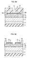
- Fig. 16 is a sectional view showing a structure of a conventional compound semiconductor device.
- An AlN layer 102, a GaN layer 103, an n-type AlGaN layer 104a, an n-type AlGaN layer 104b and an n-type GaN layer 105 are sequentially formed on an SiC substrate 101.
- a thickness of the AlN layer 102 is 150 ⁇ m.
- a total thickness of the n-type AlGaN layer 104b and the n-type GaN layer 105 is approximately 30 nm.
- an SiN layer 107 is formed on the n-type GaN layer 105.
- Plural openings are formed at the SiN layer 107, and a source electrode 108a, a drain electrode 108b and a gate electrode 109 are evaporated in these openings.
- this compound semiconductor device is a normally-on type.
- a compound semiconductor device is used for automobile parts. Current continues to flow in the automobile parts when a car goes out of order resulting from a traffic accident and so on when the compound semiconductor device is the normally-on type. Accordingly, a demand for a normally-off type compound semiconductor device becomes high in recent times.
- a positive gate leakage current flows in a saturation region as input power is made large. This is because the gate electrode 109 and the n-type GaN layer 105 are in contact directly. It is difficult to continue to use in a saturation power state if the gate leak current as stated above flows, and it is hard to say that it is suitable for the base station amplifier of the cellular phone.
- Patent Document 1 Japanese Patent Application Laid-open No. 2002-359256
- Patent Document 2 Japanese Patent Application Laid-open No. 2004-342907
- An object of the present invention is to provide a compound semiconductor device and a manufacturing method thereof capable of suppressing current flowing when a gate voltage is set to be "0" (zero), and manufacturing with high reproducibility.
- a GaN based carrier transit layer is formed on a semiconductor substrate, a GaN based carrier supply layer is formed on the carrier transit layer, a GaN based protective layer is formed on the carrier supply layer, and a source electrode, a drain electrode and a gate electrode are formed on the protective layer.
- a compound semiconductor layer containing nitrogen and positioning between the gate electrode and the source electrode, and between the gate electrode and the drain electrode, is formed on the protective layer, and an insulator layer is formed on the compound semiconductor layer.
- a GaN based carrier transit layer is formed on a semiconductor substrate, and thereafter, a GaN based carrier supply layer is formed on the carrier transit layer.
- a GaN based protective layer is formed on the carrier supply layer.
- a compound semiconductor layer containing nitrogen is formed on the protective layer.
- an insulator layer is formed on the compound semiconductor layer.
- an opening for a source electrode, an opening for a drain electrode and an opening for a gate electrode are formed in the insulator layer and the compound semiconductor layer.
- electrodes are formed in the three openings. In forming the opening for a gate electrode, wet etching of the compound semiconductor layer is performed until the protective layer exposes.
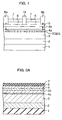
- FIG. 1 is a sectional view showing a structure of a compound semiconductor device according to the first embodiment of the present invention.
- an AlN layer 2 with a thickness of approximately 150 nm to 300 nm is formed on an SiC substrate 1.
- a GaN buffer layer 3 (a carrier transit layer) with a thickness of approximately 3 ⁇ m is formed on the AlN layer 2.
- a non-doped AlGaN layer 4a with a thickness of approximately 5 nm is formed on the GaN buffer layer 3.
- An n-type AlGaN layer 4b (a carrier supply layer) with a thickness of approximately 15 nm to 20 nm is formed on the non-doped AlGaN layer 4a.
- the n-type AlGaN layer 4b is doped with Si at approximately 4 ⁇ 10 18 cm -3 .
- an n-type GaN layer 5 (a protective layer) with a thickness of approximately 7 nm is formed on the n-type AlGaN layer 4b.
- the n-type GaN layer 5 is doped with Si at approximately 5 ⁇ 10 18 cm -3 .
- a non-doped AlN layer 6 with a thickness of approximately 3 nm and an SiN layer 7 with a thickness of approximately 20 nm are sequentially formed on the n-type GaN layer 5.
- a semiconductor-insulator junction exists between the non-doped AlN layer 6 and the SiN layer 7.
- At least three openings are formed in the non-doped AlN layer 6 and the SiN layer 7, and a source electrode 8a, a drain electrode 8b and a gate electrode 19 are evaporated in these openings.
- a semiconductor-metal junction exists between the non-doped AlN layer 6 and the gate electrode 19.
- a metal-semiconductor junction exists between the gate electrode 19 and the n-type GaN layer 5.
- the source electrode 8a and the drain electrode 8b may be composed of, for example, a Ta film with a thickness of approximately 10 nm and an Al film with a thickness of approximately 300 nm formed thereon.
- the gate electrode 19 may be composed of, for example, an Ni film and an Au film formed thereon.
- a piezoelectric effect resulting from a lattice mismatch occurs in a vicinity of an interface of the non-doped AlGaN layer 4a with the GaN buffer layer 3. Accordingly, positive polarization charges appear, and electrons are induced in the vicinity of the interface of the GaN buffer layer 3 with the non-doped AlGaN layer 4a. As a result, a two-dimensional electron gas (2DEG) appears.
- 2DEG two-dimensional electron gas
- the SiN layer 7 exists at a periphery of the gate electrode 19 as an insulator layer, and therefore, it is possible to prevent a gate leak current from a side surface. Accordingly, a high withstand voltage is realized.
- the non-doped AlN layer 6 exists between the SiN layer 7 and the n-type GaN layer 5, and therefore, electrons exist at an interface between the non-doped AlN layer 6 and the n-type GaN layer 5. Accordingly, a lot of two-dimensional electron gas exists at an electron transit region between the gate electrode 19 and the source electrode 8a and the drain electrode 8b. Consequently, a transconductance (Gm) improves, and on-resistance is suppressed to be low. Besides, a threshold voltage approximates to "0" (zero) V more closely because a gate recess structure is adopted. Namely, it becomes possible to secure the enough current while approximating the threshold voltage to "0" (zero) V owing to these interactions.
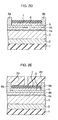
- FIG. 2A to Fig. 2G are sectional views showing the manufacturing method of the compound semiconductor device according to the first embodiment of the present invention in process sequence.
- the AlN layer 2 is formed on the SiC substrate 1, as shown in Fig. 2A .
- the GaN buffer layer 3 is formed on the AlN layer 2.
- the non-doped AlGaN layer 4a is formed on the GaN buffer layer 3.
- the n-type AlGaN layer 4b is formed on the non-doped AlGaN layer 4a.
- the n-type GaN layer 5 is formed on the n-type AlGaN layer 4b.
- the non-doped AlN layer 6 is formed on the n-type GaN layer 5.
- the SiN layer 7 is formed on the non-doped AlN layer 6.
- the formations of the AlN layer 2, the GaN buffer layer 3, the non-doped AlGaN layer 4a, the n-type AlGaN layer 4b, the n-type GaN layer 5 and the non-doped AlN layer 6 may be performed by, for example, a crystal growth method such as an MOCVD method.
- the formation of the SiN layer 7 may be performed by, for example, a plasma CVD method.
- a resist pattern 21 having openings at regions where the source electrode 8a and the drain electrode 8b are to be formed is formed on the SiN layer 7, as shown in Fig. 2B .
- wet etching of the SiN layer 7 and the non-doped AlN layer 6 is performed by using the resist pattern 21 as a mask, and thereby, the opening for the source electrode and the opening for the drain electrode are formed in the SiN layer 7 and the non-doped AlN layer 6, as shown in Fig. 2C .
- the n-type GaN layer 5 positioning under the non-doped AlN layer 6 is not removed by the wet etching, and therefore, the etching is stopped at a surface of the n-type GaN layer 5.
- the resist pattern 21 is removed after the openings are formed.
- the source electrode 8a and the drain electrode 8b are evaporated in the openings in the SiN layer 7 and the non-doped AlN layer 6, as shown in Fig. 2D .
- a resist pattern 22 having an opening at a region where the gate electrode 19 is to be formed is formed on the SiN layer 7, the source electrode 8a and the drain electrode 8b, as shown in Fig. 2E .
- wet etching etching using acid
- wet etching using acid of the SiN layer 7 and the non-doped AlN layer 6 is performed by using the resist pattern 22 as a mask, and thereby, the opening for the gate electrode is formed in the SiN layer 7 and the non-doped AlN layer 6, as shown in Fig. 2F .
- the n-type GaN layer 5 positioning under the non-doped AlN layer 6 is not removed by the wet etching, and therefore, the etching is stopped at the surface of the n-type GaN layer 5.
- the resist pattern 22 is removed after the opening is formed.
- the gate electrode 19 (an embedded gate electrode) is evaporated in the opening in the SiN layer 7 and the non-doped AlN layer 6, as shown in Fig. 2G .
- element isolation can be performed by, for example, ion-implantation, though it is not shown.
- a selection ratio between the non-doped AlN layer 6 and the n-type GaN layer 5 at the wet etching is high, and therefore, it is possible to process the non-doped AlN layer 6 with high accuracy. Accordingly, it is possible to form the gate electrode 19 having good reproducibility with high accuracy.
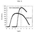
- Fig. 3 is a graphic chart showing the device characteristic of the compound semiconductor device according to the first embodiment measured by the present inventor.
- a device characteristic of the conventional compound semiconductor device shown in Fig. 16 is also shown in Fig. 3 for the purpose of reference.
- a horizontal axis is a voltage between gate-source (Vgs), and a vertical axis is a transconductance (Gm).
- Vgs gate-source
- Gm transconductance
- the threshold voltage approximates to "0" (zero) V more closely in the first embodiment compared to the conventional compound semiconductor device.
- bottom surfaces of the source electrode 8a and the drain electrode 8b are in contact with the surface of the n-type GaN layer 5, but they may be in contact with a surface of the n-type AlGaN layer 4b as shown in Fig. 15 .
- the opening for the source electrode and the opening for the drain electrode are formed in the SiN layer 7 and the non-doped AlN layer 6 by using the resist pattern 21 shown in Fig. 2B as the mask, and thereafter, a dry etching of the n-type GaN layer 5 is performed while remaining the resist pattern 21.
- a reactive ion etching is performed, for example, with a pressure of 2 Pa, a Cl 2 flow rate of 10 sccm, and an etching speed of 10 nm/min.
- An end point of the dry etching may be determined by, for example, a time control.
- an error of an etching amount is preferable to be within ⁇ 3 nm.
- the source electrode 8a and the drain electrode 8b may be composed of, for example, a Ta film with a thickness of approximately 10 nm and an Al film with a thickness of approximately 300 nm formed thereon.
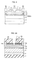
- FIG. 4 is a sectional view showing a structure of a compound semiconductor device according to the second embodiment of the present invention.
- the opening for the gate electrode of the non-doped AlN layer 6 is approximately equal to that of the first embodiment, the opening for the gate electrode of the SiN layer 7 is wider than that of the first embodiment.
- a gate electrode 29 having an overhang portion is embedded in the opening.
- the other structure is the same as the first embodiment.
- an electric field concentration in a vicinity of an interface between the gate electrode 29 and the non-doped AlN layer 6 is reduced than the electric field concentration in a vicinity of an interface between the gate electrode 19 and the non-doped AlN layer 6 in the first embodiment.
- a voltage of 50 V to 500 V is applied between the gate and drain in the compound semiconductor device, but according to the second embodiment, deterioration hardly occurs furthermore even in the case as stated above.
- FIG. 5A to Fig. 5C are sectional views showing the manufacturing method of the compound semiconductor device according to the second embodiment of the present invention in process sequence.
- a resist pattern 23 having an opening at a region where the overhang portion of the gate electrode 29 is to be formed is formed on the SiN layer 7, the source electrode 8a and the drain electrode 8b, as shown in Fig. 5A .
- wet etching of the SiN layer 7 is performed by using the resist pattern 23 as a mask, and thereby, the opening for the overhang portion is formed in the SiN layer 7, as shown in Fig. 5B .
- the resist pattern 23 is removed after the opening is formed.
- the gate electrode 29 (an embedded gate electrode) is evaporated in the opening in the SiN layer 7 and the non-doped AlN layer 6, as shown in Fig. 5C .
- element isolation can be performed by, for example, ion-implantation, though it is not shown.
- Fig. 6 is a graphic chart showing the device characteristic of the compound semiconductor device according to the second embodiment measured by the present inventor.
- a device characteristic of the conventional compound semiconductor device shown in Fig. 16 is also shown for the purpose of reference.
- a horizontal axis is a voltage between gate-drain (Vgd), and a vertical axis is a current between gate-drain (Igd).
- Vgd gate-drain
- Igd current between gate-drain
- a backward gate leak current decreases in the second embodiment compared to the conventional compound semiconductor device.
- the threshold voltage approximates to "0" (zero) V without decreasing saturation current.
- a third embodiment of the present invention is described.
- an MIS (Metal-Insulator-Semiconductor) structure is adopted.
- Fig. 7 is a sectional view showing the structure of a compound semiconductor device according to the third embodiment of the present invention.
- an SiN layer 7a with a thickness of approximately 10 nm is formed on the non-doped AlN layer 6. At least three openings (for a source electrode, for a drain electrode and for a gate electrode) are formed in the non-doped AlN layer 6 and the SiN layer 7a. In the present embodiment, an SiN layer 7b with a thickness of approximately 10 nm is formed in the opening for the gate electrode among the three openings, and on the SiN layer 7a. A gate electrode 39 having an overhang portion is evaporated in the opening for the gate electrode.
- the other structure is the same as the first embodiment.
- a forward gate leak current can be drastically reduced. Besides, a complete normally-off operation can be performed. Besides, it becomes possible to obtain high current because the normally-off operation is realized.
- FIG. 8A to Fig. 8E are sectional views showing the manufacturing method of the compound semiconductor device according to the third embodiment of the present invention in process sequence.
- the processes until the formation of the non-doped AlN layer 6 are performed as same as the first embodiment.
- the SiN layer 7a is formed on the non-doped AlN layer 6, as shown in Fig. 8A .
- the formation of the SiN layer 7a may be performed by, for example, a plasma CVD method.
- a resist pattern 24 having an opening at a region where a lower portion of the gate electrode 39 is to be formed is formed on the SiN layer 7a, the source electrode 8a and the drain electrode 8b, as shown in Fig. 8B .
- wet etching of the SiN layer 7a and the non-doped AlN layer 6 is performed by using the resist pattern 24 as a mask, and thereby, the opening for the gate electrode is formed in the SiN layer 7a and the non-doped AlN layer 6, as shown in Fig. 8C .
- the n-type GaN layer 5 positioning under the non-doped AlN layer 6 is not removed by the wet etching, and therefore, the etching is stopped at the surface of the n-type GaN layer 5.
- the resist pattern 24 is removed after the opening is formed.
- the SiN layer 7b is formed in the opening for the gate electrode and on the SiN layer 7a, as shown in Fig. 8D .
- the formation of the SiN layer 7b may be performed by, for example, a plasma CVD method.
- the gate electrode 39 (an embedded gate electrode) is evaporated in the opening in the SiN layer 7a and the non-doped AlN layer 6, as shown in Fig. 8E .
- element isolation can be performed by, for example, ion-implantation, though it is not shown.
- Fig. 9 is a graphic chart showing the device characteristic of the compound semiconductor device according to the third embodiment measured by the present inventor.
- a device characteristic of the conventional compound semiconductor device shown in Fig. 16 is also shown for the purpose of reference.
- a horizontal axis is a gate voltage
- a vertical axis is a forward gate leak current.
- the forward gate leak current is reduced in the third embodiment compared to the conventional compound semiconductor device. Namely, in the third embodiment, the gate leak current scarcely flows even when the gate voltage is increased up to approximately 4 V.
- a threshold voltage Vth a threshold voltage Vth, a variation thereof ⁇ vth and a maximum current Imax
- Table 1 device characteristics of the conventional compound semiconductor device shown in Fig. 16 are also shown for the purpose of reference.
- the threshold voltage Vth is a negative value in the conventional compound semiconductor device
- the threshold voltage Vth is a positive value in the third embodiment.
- the variation ⁇ vth of the threshold voltage in the third embodiment is approximately 1/10 of the conventional compound semiconductor device. This is because it is possible to form the structure in the vicinity of the gate electrode 39 with high reproducibility in the third embodiment, but the reproducibility is low in the conventional compound semiconductor device.
- the maximum current Imax becomes extremely high compared to the conventional compound semiconductor device in accordance with the reduction of the gate leak current.
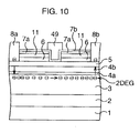
- FIG. 10 is a sectional view showing a structure of a compound semiconductor device according to the fourth embodiment of the present invention.
- an n-type GaN layer 11 with a thickness of approximately 7 nm is formed between the non-doped AlN layer 6 and the SiN layer 7a.
- the n-type GaN layer 11 is doped with Si at approximately 5 ⁇ 10 18 cm -3 .
- An opening similar to those of the non-doped AlN layer 6 and the SiN layer 7a are formed in the n-type GaN layer 11.
- the other structure is the same as the third embodiment.
- a doping amount of Si in the n-type GaN layer 11 may be higher than that of the n-type GaN layer 5.
- the n-type GaN layer 11 is formed on the non-doped AlN layer 6, and therefore, a chemical change of the non-doped AlN layer 6 hardly occurs. Accordingly, deterioration of a whole device hardly occurs, and a high reliability can be obtained.
- the n-type GaN layer 11 is formed on the non-doped AlN layer 6 between the formation of the non-doped AlN layer 6 and the formation of the SiN layer 7a.
- dry etching of the n-type GaN layer 11 is performed. This dry etching may be performed by a time control.
- wet etching of the non-doped AlN layer 6 is performed as same as the first to third embodiments. At this time, the n-type GaN layer 5 positioning under the non-doped AlN layer 6 is not removed by the wet etching, and therefore, the etching is stopped at the surface of the n-type GaN layer 5.
- Fig. 11 is a graphic chart showing a test data of the reliability of the compound semiconductor device according to the fourth embodiment measured by the present inventor.
- test data three kinds of the conventional compound semiconductor device shown in Fig. 16 are shown for the purpose of reference.
- a horizontal axis is test time
- a vertical axis is a gate leak current Ig.
- the gate leak currents are high even at a test start time, and the gate leak currents increase as the time elapses depending on samples, in the conventional compound semiconductor device. This shows that the deterioration is in progress.
- the gate leak current at the test start time is low, and further, the increase in accordance with the elapsed time is not observed at all.
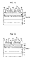
- Fig. 12 is a sectional view showing a structure of a compound semiconductor device according to the fifth embodiment.
- a non-doped GaN layer 12 is formed instead of the n-type GaN layer 5 in the fourth embodiment.
- the non-doped GaN layer 12 is used instead of the n-type GaN layer 5, and therefore, the gate leak current can be reduced further more.
- the MIS structure is adopted as same as the third embodiment, and therefore, the characteristics may not deteriorate even if the non-doped GaN layer 12 is used.
- FIG. 13 is a sectional view showing a structure of a compound semiconductor device according to the sixth embodiment of the present invention.
- an n-type InGaN layer 13 is formed instead of the n-type GaN layer 11 in the fifth embodiment.
- the n-type InGaN layer 13 is used instead of the n-type GaN layer 11, and therefore, a band in this layer decreases, and the two-dimensional electron gas increases. As a result, the maximum current increases.
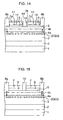
- Fig. 14 is a sectional view showing a structure of a compound semiconductor device according to the seventh embodiment of the present invention.
- an Si layer 14 for one atomic layer is formed between the non-doped AlN layer 6 and the n-type GaN layer 11 in the fourth embodiment.
- the Si layer 14 may be formed by, for example, a planer doping method (an atomic layer doping method).
- the Si layer 14 may be formed between the n-type GaN layer 5 and the non-doped AlN layer 6.
- the formation of the AlN layer may be performed by an ALD (Atomic Layer Deposition) method, a sputtering method, or the like.
- ALD Atomic Layer Deposition
- the AlN layer is formed between the gate electrode, the source electrode and the drain electrode as a compound semiconductor layer containing N, but another compound semiconductor layer, for example, a layer such as InAlN further containing In may be formed.
- the element isolation may be performed by, for example, the ion-implantation, a mesa etching, or the like.
- a compound semiconductor layer containing N is formed on a protective layer, and a process of the compound semiconductor layer can be performed under a condition free from an influence on the protective layer. Accordingly, it is possible to construct a gate recess structure with high reproducibility. It is therefore possible to suppress current flowing when a gate voltage is made to be "0" (zero). Besides, it is possible to suppress a gate leak current to realize a high withstand voltage when an insulator layer is in contact with a side surface of a gate electrode.
Abstract
Description
- The present invention relates to a compound semiconductor device suitable for a high electron mobility transistor (HEMT) and so on and a manufacturing method thereof.
- In recent years, a development of an electronic device (a compound semiconductor device) is vigorous in which a GaN layer and an AlGaN layer are formed sequentially on a substrate composed of sapphire, SiC, GaN, Si, or the like, and the GaN layer is used as an electron transit layer. A bandgap of GaN is 3.4 eV, and it is larger than that of GaAs of 1.4 eV. Accordingly, an operation in high withstand voltage is expected for the compound semiconductor device.
- A high-voltage operation is required for a base station amplifier of a cellular phone system, and a high withstand voltage is essential requirement thereof. At present, a value over 300 V is reported as a withstand voltage when current is turned off. There is a case when a change in on-resistance during operation called as a current collapse occurs in the above-stated compound semiconductor device. This phenomenon can be avoided by disposing a GaN protective layer on an AlGaN electron supply layer, and further forming an SiN protective film. The structure as stated above is described in, for example,
Patent Document 1. -
Fig. 16 is a sectional view showing a structure of a conventional compound semiconductor device. AnAlN layer 102, aGaN layer 103, an n-type AlGaN layer 104a, an n-type AlGaN layer 104b and an n-type GaN layer 105 are sequentially formed on anSiC substrate 101. A thickness of theAlN layer 102 is 150 µm. A total thickness of the n-type AlGaN layer 104b and the n-type GaN layer 105 is approximately 30 nm. Further, anSiN layer 107 is formed on the n-type GaN layer 105. Plural openings are formed at theSiN layer 107, and asource electrode 108a, adrain electrode 108b and agate electrode 109 are evaporated in these openings. - But, this compound semiconductor device is a normally-on type. There is a case when a compound semiconductor device is used for automobile parts. Current continues to flow in the automobile parts when a car goes out of order resulting from a traffic accident and so on when the compound semiconductor device is the normally-on type. Accordingly, a demand for a normally-off type compound semiconductor device becomes high in recent times.
- It is necessary to make a threshold voltage positive to realize the normally-off type compound semiconductor device. Accordingly, a recess gate structure is proposed. However, it is difficult to manufacture a compound semiconductor device in the recess gate structure with high accuracy. This is because a selective etching suitable for processing each semiconductor layer constituting the compound semiconductor device has not been found, and instead, a time-controlled dry etching is performed.
- Besides, in the conventional compound semiconductor device shown in
Fig. 16 , a positive gate leakage current flows in a saturation region as input power is made large. This is because thegate electrode 109 and the n-type GaN layer 105 are in contact directly. It is difficult to continue to use in a saturation power state if the gate leak current as stated above flows, and it is hard to say that it is suitable for the base station amplifier of the cellular phone. - Accordingly, a structure in which an insulator layer is sandwiched between the n-
type GaN layer 105 and thegate electrode 109 is proposed. However, when the insulator layer exists, the gate leak current decreases, but the threshold voltage becomes deep. Accordingly, it is considered that the threshold voltage cannot be made positive with this structure. Further, the withstand voltage decreases though the gate leak current is reduced. This is caused by an influence of a trap between the insulator layer and the n-type GaN layer 105. - Patent Document 1: Japanese Patent Application Laid-open No.
2002-359256
Patent Document 2: Japanese Patent Application Laid-open No.2004-342907 - An object of the present invention is to provide a compound semiconductor device and a manufacturing method thereof capable of suppressing current flowing when a gate voltage is set to be "0" (zero), and manufacturing with high reproducibility.
- In order to solve the above problems, the inventor of the present invention has conducted dedicated studies and consequently reached several aspects of the invention as follows.
- In a compound semiconductor device according to the present invention, a GaN based carrier transit layer is formed on a semiconductor substrate, a GaN based carrier supply layer is formed on the carrier transit layer, a GaN based protective layer is formed on the carrier supply layer, and a source electrode, a drain electrode and a gate electrode are formed on the protective layer. Besides, a compound semiconductor layer containing nitrogen and positioning between the gate electrode and the source electrode, and between the gate electrode and the drain electrode, is formed on the protective layer, and an insulator layer is formed on the compound semiconductor layer.
- In a manufacturing method of a compound semiconductor device according to the present invention, a GaN based carrier transit layer is formed on a semiconductor substrate, and thereafter, a GaN based carrier supply layer is formed on the carrier transit layer. Next, a GaN based protective layer is formed on the carrier supply layer. Subsequently, a compound semiconductor layer containing nitrogen is formed on the protective layer. After that, an insulator layer is formed on the compound semiconductor layer. Subsequently, an opening for a source electrode, an opening for a drain electrode and an opening for a gate electrode are formed in the insulator layer and the compound semiconductor layer. Next, electrodes are formed in the three openings. In forming the opening for a gate electrode, wet etching of the compound semiconductor layer is performed until the protective layer exposes.
-
-
Fig. 1 is a sectional view showing a structure of a compound semiconductor device according to a first embodiment of the present invention; -
Fig. 2A is a sectional view showing a manufacturing method of the compound semiconductor device according to the first embodiment of the present invention; -
Fig. 2B is a sectional view showing the manufacturing method of the compound semiconductor device subsequent toFig. 2A ; -
Fig. 2C is a sectional view showing the manufacturing method of the compound semiconductor device subsequent toFig. 2B ; -
Fig. 2D is a sectional view showing the manufacturing method of the compound semiconductor device subsequent toFig. 2C ; -
Fig. 2E is a sectional view showing the manufacturing method of the compound semiconductor device subsequent toFig. 2D ; -
Fig. 2F is a sectional view showing the manufacturing method of the compound semiconductor device subsequent toFig. 2E ; -
Fig. 2G is a sectional view showing the manufacturing method of the compound semiconductor device subsequent toFig. 2F ; -
Fig. 3 is a graphic chart showing a device characteristic of the compound semiconductor device according to the first embodiment of the present invention; -
Fig. 4 is a sectional view showing a structure of a compound semiconductor device according to a second embodiment of the present invention; -
Fig. 5A is a sectional view showing a manufacturing method of the compound semiconductor device according to the second embodiment of the present invention; -
Fig. 5B is a sectional view showing the manufacturing method of the compound semiconductor device subsequent toFig. 5A ; -
Fig. 5C is a sectional view showing the manufacturing method of the compound semiconductor device subsequent toFig. 5B ; -
Fig. 6 is a graphic chart showing a device characteristic of the compound semiconductor device according to the second embodiment of the present invention; -
Fig. 7 is a sectional view showing a structure of a compound semiconductor device according to a third embodiment of the present invention; -
Fig. 8A is a sectional view showing a manufacturing method of the compound semiconductor device according to the third embodiment of the present invention; -
Fig. 8B is a sectional view showing the manufacturing method of the compound semiconductor device subsequent toFig. 8A ; -
Fig. 8C is a sectional view showing the manufacturing method of the compound semiconductor device subsequent toFig. 8B ; -
Fig. 8D is a sectional view showing the manufacturing method of the compound semiconductor device subsequent toFig. 8C ; -
Fig. 8E is a sectional view showing the manufacturing method of the compound semiconductor device subsequent toFig. 8D ; -
Fig. 9 is a graphic chart showing a device characteristic of the compound semiconductor device according to the third embodiment of the present invention; -
Fig. 10 is a sectional view showing a structure of a compound semiconductor device according to a fourth embodiment of the present invention; -
Fig. 11 is a graphic chart showing a test data of reliability of the compound semiconductor device according to the fourth embodiment of the present invention; -
Fig. 12 is a sectional view showing a structure of a compound semiconductor device according to a fifth embodiment of the present invention; -
Fig. 13 is a sectional view showing a structure of a compound semiconductor device according to a sixth embodiment of the present invention; -
Fig. 14 is a sectional view showing a structure of a compound semiconductor device according to a seventh embodiment of the present invention; -
Fig. 15 is a sectional view showing a modification example of the first embodiment of the present invention; and -
Fig. 16 is a sectional view showing a structure of a conventional compound semiconductor device. - Hereinafter, embodiments of the present invention are concretely described with reference to the attached drawings.
- First, a first embodiment of the present invention is described.
Fig. 1 is a sectional view showing a structure of a compound semiconductor device according to the first embodiment of the present invention. - In the first embodiment, an
AlN layer 2 with a thickness of approximately 150 nm to 300 nm is formed on anSiC substrate 1. A GaN buffer layer 3 (a carrier transit layer) with a thickness of approximately 3 µm is formed on theAlN layer 2. Anon-doped AlGaN layer 4a with a thickness of approximately 5 nm is formed on theGaN buffer layer 3. An n-type AlGaN layer 4b (a carrier supply layer) with a thickness of approximately 15 nm to 20 nm is formed on thenon-doped AlGaN layer 4a. The n-type AlGaN layer 4b is doped with Si at approximately 4×1018 cm-3. Further, an n-type GaN layer 5 (a protective layer) with a thickness of approximately 7 nm is formed on the n-type AlGaN layer 4b. The n-type GaN layer 5 is doped with Si at approximately 5×1018 cm-3. Anon-doped AlN layer 6 with a thickness of approximately 3 nm and anSiN layer 7 with a thickness of approximately 20 nm are sequentially formed on the n-type GaN layer 5. A semiconductor-insulator junction exists between thenon-doped AlN layer 6 and theSiN layer 7. At least three openings (for a source electrode, for a drain electrode and for a gate electrode) are formed in thenon-doped AlN layer 6 and theSiN layer 7, and asource electrode 8a, adrain electrode 8b and agate electrode 19 are evaporated in these openings. A semiconductor-metal junction exists between thenon-doped AlN layer 6 and thegate electrode 19. Besides, a metal-semiconductor junction exists between thegate electrode 19 and the n-type GaN layer 5. Thesource electrode 8a and thedrain electrode 8b may be composed of, for example, a Ta film with a thickness of approximately 10 nm and an Al film with a thickness of approximately 300 nm formed thereon. Besides, thegate electrode 19 may be composed of, for example, an Ni film and an Au film formed thereon. - In the first embodiment as stated above, a piezoelectric effect resulting from a lattice mismatch occurs in a vicinity of an interface of the
non-doped AlGaN layer 4a with theGaN buffer layer 3. Accordingly, positive polarization charges appear, and electrons are induced in the vicinity of the interface of theGaN buffer layer 3 with thenon-doped AlGaN layer 4a. As a result, a two-dimensional electron gas (2DEG) appears. - Besides, the
SiN layer 7 exists at a periphery of thegate electrode 19 as an insulator layer, and therefore, it is possible to prevent a gate leak current from a side surface. Accordingly, a high withstand voltage is realized. - Further, the
non-doped AlN layer 6 exists between theSiN layer 7 and the n-type GaN layer 5, and therefore, electrons exist at an interface between thenon-doped AlN layer 6 and the n-type GaN layer 5. Accordingly, a lot of two-dimensional electron gas exists at an electron transit region between thegate electrode 19 and thesource electrode 8a and thedrain electrode 8b. Consequently, a transconductance (Gm) improves, and on-resistance is suppressed to be low. Besides, a threshold voltage approximates to "0" (zero) V more closely because a gate recess structure is adopted. Namely, it becomes possible to secure the enough current while approximating the threshold voltage to "0" (zero) V owing to these interactions. - Next, a manufacturing method of the compound semiconductor device according to the first embodiment is described.
Fig. 2A to Fig. 2G are sectional views showing the manufacturing method of the compound semiconductor device according to the first embodiment of the present invention in process sequence. - First, the
AlN layer 2 is formed on theSiC substrate 1, as shown inFig. 2A . Next, theGaN buffer layer 3 is formed on theAlN layer 2. Subsequently, thenon-doped AlGaN layer 4a is formed on theGaN buffer layer 3. After that, the n-type AlGaN layer 4b is formed on thenon-doped AlGaN layer 4a. Subsequently, the n-type GaN layer 5 is formed on the n-type AlGaN layer 4b. Next, thenon-doped AlN layer 6 is formed on the n-type GaN layer 5. Next, theSiN layer 7 is formed on thenon-doped AlN layer 6. The formations of theAlN layer 2, theGaN buffer layer 3, thenon-doped AlGaN layer 4a, the n-type AlGaN layer 4b, the n-type GaN layer 5 and thenon-doped AlN layer 6 may be performed by, for example, a crystal growth method such as an MOCVD method. Besides, the formation of theSiN layer 7 may be performed by, for example, a plasma CVD method. - Next, a resist
pattern 21 having openings at regions where thesource electrode 8a and thedrain electrode 8b are to be formed is formed on theSiN layer 7, as shown inFig. 2B . - Subsequently, wet etching of the
SiN layer 7 and thenon-doped AlN layer 6 is performed by using the resistpattern 21 as a mask, and thereby, the opening for the source electrode and the opening for the drain electrode are formed in theSiN layer 7 and thenon-doped AlN layer 6, as shown inFig. 2C . At this time, the n-type GaN layer 5 positioning under thenon-doped AlN layer 6 is not removed by the wet etching, and therefore, the etching is stopped at a surface of the n-type GaN layer 5. The resistpattern 21 is removed after the openings are formed. - After that, the
source electrode 8a and thedrain electrode 8b are evaporated in the openings in theSiN layer 7 and thenon-doped AlN layer 6, as shown inFig. 2D . - Subsequently, a resist
pattern 22 having an opening at a region where thegate electrode 19 is to be formed is formed on theSiN layer 7, thesource electrode 8a and thedrain electrode 8b, as shown inFig. 2E . - Next, wet etching (etching using acid) of the
SiN layer 7 and thenon-doped AlN layer 6 is performed by using the resistpattern 22 as a mask, and thereby, the opening for the gate electrode is formed in theSiN layer 7 and thenon-doped AlN layer 6, as shown inFig. 2F . At this time also, the n-type GaN layer 5 positioning under thenon-doped AlN layer 6 is not removed by the wet etching, and therefore, the etching is stopped at the surface of the n-type GaN layer 5. The resistpattern 22 is removed after the opening is formed. - Subsequently, the gate electrode 19 (an embedded gate electrode) is evaporated in the opening in the
SiN layer 7 and thenon-doped AlN layer 6, as shown inFig. 2G . Incidentally, element isolation can be performed by, for example, ion-implantation, though it is not shown. - According to the manufacturing method as stated above, a selection ratio between the
non-doped AlN layer 6 and the n-type GaN layer 5 at the wet etching is high, and therefore, it is possible to process thenon-doped AlN layer 6 with high accuracy. Accordingly, it is possible to form thegate electrode 19 having good reproducibility with high accuracy. - Here, a device characteristic of the compound semiconductor device manufactured by the present inventor in accordance with the above-stated method is described.
Fig. 3 is a graphic chart showing the device characteristic of the compound semiconductor device according to the first embodiment measured by the present inventor. A device characteristic of the conventional compound semiconductor device shown inFig. 16 is also shown inFig. 3 for the purpose of reference. A horizontal axis is a voltage between gate-source (Vgs), and a vertical axis is a transconductance (Gm). As shown inFig. 3 , the threshold voltage approximates to "0" (zero) V more closely in the first embodiment compared to the conventional compound semiconductor device. - Incidentally, in the first embodiment, bottom surfaces of the
source electrode 8a and thedrain electrode 8b are in contact with the surface of the n-type GaN layer 5, but they may be in contact with a surface of the n-type AlGaN layer 4b as shown inFig. 15 . In this case, for example, the opening for the source electrode and the opening for the drain electrode are formed in theSiN layer 7 and thenon-doped AlN layer 6 by using the resistpattern 21 shown inFig. 2B as the mask, and thereafter, a dry etching of the n-type GaN layer 5 is performed while remaining the resistpattern 21. In the dry etching, a reactive ion etching (RIE) is performed, for example, with a pressure of 2 Pa, a Cl2 flow rate of 10 sccm, and an etching speed of 10 nm/min. An end point of the dry etching may be determined by, for example, a time control. Incidentally, an error of an etching amount is preferable to be within ±3 nm. In this case also, thesource electrode 8a and thedrain electrode 8b may be composed of, for example, a Ta film with a thickness of approximately 10 nm and an Al film with a thickness of approximately 300 nm formed thereon. The structures of the electrodes and the periphery thereof as stated above can be applied to the following embodiments. - Next, a second embodiment of the present invention is described.
Fig. 4 is a sectional view showing a structure of a compound semiconductor device according to the second embodiment of the present invention. - In the second embodiment, although a size of the opening for the gate electrode of the
non-doped AlN layer 6 is approximately equal to that of the first embodiment, the opening for the gate electrode of theSiN layer 7 is wider than that of the first embodiment. Agate electrode 29 having an overhang portion is embedded in the opening. The other structure is the same as the first embodiment. - According to the second embodiment as stated above, an electric field concentration in a vicinity of an interface between the
gate electrode 29 and thenon-doped AlN layer 6 is reduced than the electric field concentration in a vicinity of an interface between thegate electrode 19 and thenon-doped AlN layer 6 in the first embodiment. There is a case when a voltage of 50 V to 500 V is applied between the gate and drain in the compound semiconductor device, but according to the second embodiment, deterioration hardly occurs furthermore even in the case as stated above. - Next, a manufacturing method of the compound semiconductor device according to the second embodiment is described.
Fig. 5A to Fig. 5C are sectional views showing the manufacturing method of the compound semiconductor device according to the second embodiment of the present invention in process sequence. - First, the processes until the removal of the resist pattern 22 (refer to
Fig. 2F ) are performed as same as the first embodiment. Next, a resistpattern 23 having an opening at a region where the overhang portion of thegate electrode 29 is to be formed is formed on theSiN layer 7, thesource electrode 8a and thedrain electrode 8b, as shown inFig. 5A . - Next, wet etching of the
SiN layer 7 is performed by using the resistpattern 23 as a mask, and thereby, the opening for the overhang portion is formed in theSiN layer 7, as shown inFig. 5B . The resistpattern 23 is removed after the opening is formed. - Subsequently, the gate electrode 29 (an embedded gate electrode) is evaporated in the opening in the
SiN layer 7 and thenon-doped AlN layer 6, as shown inFig. 5C . Incidentally, element isolation can be performed by, for example, ion-implantation, though it is not shown. - Here, a device characteristic of the compound semiconductor device manufactured by the present inventor in accordance with the above-stated method is described.
Fig. 6 is a graphic chart showing the device characteristic of the compound semiconductor device according to the second embodiment measured by the present inventor. InFig. 6 , a device characteristic of the conventional compound semiconductor device shown inFig. 16 is also shown for the purpose of reference. A horizontal axis is a voltage between gate-drain (Vgd), and a vertical axis is a current between gate-drain (Igd). As shown inFig. 6 , a backward gate leak current decreases in the second embodiment compared to the conventional compound semiconductor device. Further, the threshold voltage approximates to "0" (zero) V without decreasing saturation current. - Next, a third embodiment of the present invention is described. In the third embodiment, an MIS (Metal-Insulator-Semiconductor) structure is adopted.
Fig. 7 is a sectional view showing the structure of a compound semiconductor device according to the third embodiment of the present invention. - In the third embodiment, an
SiN layer 7a with a thickness of approximately 10 nm is formed on thenon-doped AlN layer 6. At least three openings (for a source electrode, for a drain electrode and for a gate electrode) are formed in thenon-doped AlN layer 6 and theSiN layer 7a. In the present embodiment, anSiN layer 7b with a thickness of approximately 10 nm is formed in the opening for the gate electrode among the three openings, and on theSiN layer 7a. Agate electrode 39 having an overhang portion is evaporated in the opening for the gate electrode. The other structure is the same as the first embodiment. - According to the third embodiment as stated above, a forward gate leak current can be drastically reduced. Besides, a complete normally-off operation can be performed. Besides, it becomes possible to obtain high current because the normally-off operation is realized.
- Next, a manufacturing method of the compound semiconductor device according to the third embodiment is described.
Fig. 8A to Fig. 8E are sectional views showing the manufacturing method of the compound semiconductor device according to the third embodiment of the present invention in process sequence. - First, the processes until the formation of the non-doped AlN layer 6 (refer to
Fig. 2A ) are performed as same as the first embodiment. Next, theSiN layer 7a is formed on thenon-doped AlN layer 6, as shown inFig. 8A . The formation of theSiN layer 7a may be performed by, for example, a plasma CVD method. - Next, the processes until the formations of the
source electrode 8a and thedrain electrode 8b (refer toFig. 2D ) are performed as same as the first embodiment. After that, a resistpattern 24 having an opening at a region where a lower portion of thegate electrode 39 is to be formed is formed on theSiN layer 7a, thesource electrode 8a and thedrain electrode 8b, as shown inFig. 8B . - Subsequently, wet etching of the
SiN layer 7a and thenon-doped AlN layer 6 is performed by using the resistpattern 24 as a mask, and thereby, the opening for the gate electrode is formed in theSiN layer 7a and thenon-doped AlN layer 6, as shown inFig. 8C . At this time, the n-type GaN layer 5 positioning under thenon-doped AlN layer 6 is not removed by the wet etching, and therefore, the etching is stopped at the surface of the n-type GaN layer 5. The resistpattern 24 is removed after the opening is formed. - Next, the
SiN layer 7b is formed in the opening for the gate electrode and on theSiN layer 7a, as shown inFig. 8D . The formation of theSiN layer 7b may be performed by, for example, a plasma CVD method. - Subsequently, the gate electrode 39 (an embedded gate electrode) is evaporated in the opening in the
SiN layer 7a and thenon-doped AlN layer 6, as shown inFig. 8E . Incidentally, element isolation can be performed by, for example, ion-implantation, though it is not shown. - Here, a device characteristic of the compound semiconductor device manufactured by the present inventor in accordance with the above-stated method is described.
Fig. 9 is a graphic chart showing the device characteristic of the compound semiconductor device according to the third embodiment measured by the present inventor. InFig. 9 , a device characteristic of the conventional compound semiconductor device shown inFig. 16 is also shown for the purpose of reference. A horizontal axis is a gate voltage, and a vertical axis is a forward gate leak current. As shown inFig. 9 , the forward gate leak current is reduced in the third embodiment compared to the conventional compound semiconductor device. Namely, in the third embodiment, the gate leak current scarcely flows even when the gate voltage is increased up to approximately 4 V. - Besides, device characteristics (a threshold voltage Vth, a variation thereof σvth and a maximum current Imax) of the compound semiconductor device manufactured by the present inventor in accordance with the above-stated method are shown in Table 1. In Table 1, device characteristics of the conventional compound semiconductor device shown in
Fig. 16 are also shown for the purpose of reference. Although, the threshold voltage Vth is a negative value in the conventional compound semiconductor device, the threshold voltage Vth is a positive value in the third embodiment. Besides, the variation σvth of the threshold voltage in the third embodiment is approximately 1/10 of the conventional compound semiconductor device. This is because it is possible to form the structure in the vicinity of thegate electrode 39 with high reproducibility in the third embodiment, but the reproducibility is low in the conventional compound semiconductor device. Further, in the third embodiment, the maximum current Imax becomes extremely high compared to the conventional compound semiconductor device in accordance with the reduction of the gate leak current. -
[Table 1] Third Embodiment Prior Art Vth +0.1 V -0.2 V σvth 30 mV 300 mV Imax 650 mA/ mm 100 mA/mm - Next, a fourth embodiment of the present invention is described.
Fig. 10 is a sectional view showing a structure of a compound semiconductor device according to the fourth embodiment of the present invention. - In the fourth embodiment, an n-
type GaN layer 11 with a thickness of approximately 7 nm is formed between thenon-doped AlN layer 6 and theSiN layer 7a. The n-type GaN layer 11 is doped with Si at approximately 5×1018 cm-3. An opening similar to those of thenon-doped AlN layer 6 and theSiN layer 7a are formed in the n-type GaN layer 11. The other structure is the same as the third embodiment. Incidentally, a doping amount of Si in the n-type GaN layer 11 may be higher than that of the n-type GaN layer 5. - According to the fourth embodiment as stated above, the n-
type GaN layer 11 is formed on thenon-doped AlN layer 6, and therefore, a chemical change of thenon-doped AlN layer 6 hardly occurs. Accordingly, deterioration of a whole device hardly occurs, and a high reliability can be obtained. - Incidentally, when the compound semiconductor device according to the fourth embodiment is manufactured, for example, the n-
type GaN layer 11 is formed on thenon-doped AlN layer 6 between the formation of thenon-doped AlN layer 6 and the formation of theSiN layer 7a. After the opening is formed in theSiN layer 7a, dry etching of the n-type GaN layer 11 is performed. This dry etching may be performed by a time control. Next, wet etching of thenon-doped AlN layer 6 is performed as same as the first to third embodiments. At this time, the n-type GaN layer 5 positioning under thenon-doped AlN layer 6 is not removed by the wet etching, and therefore, the etching is stopped at the surface of the n-type GaN layer 5. - Here, a reliability of the compound semiconductor device manufactured by the present inventor in accordance with the above-stated method is described.
Fig. 11 is a graphic chart showing a test data of the reliability of the compound semiconductor device according to the fourth embodiment measured by the present inventor. InFig. 11 , test data (three kinds) of the conventional compound semiconductor device shown inFig. 16 are shown for the purpose of reference. A horizontal axis is test time, and a vertical axis is a gate leak current Ig. As shown inFig. 11 , the gate leak currents are high even at a test start time, and the gate leak currents increase as the time elapses depending on samples, in the conventional compound semiconductor device. This shows that the deterioration is in progress. On the other hand, in the fourth embodiment, the gate leak current at the test start time is low, and further, the increase in accordance with the elapsed time is not observed at all. - Next, a fifth embodiment of the present invention is described.
Fig. 12 is a sectional view showing a structure of a compound semiconductor device according to the fifth embodiment. - In the fifth embodiment, a
non-doped GaN layer 12 is formed instead of the n-type GaN layer 5 in the fourth embodiment. - According to the fifth embodiment as stated above, the
non-doped GaN layer 12 is used instead of the n-type GaN layer 5, and therefore, the gate leak current can be reduced further more. Besides, the MIS structure is adopted as same as the third embodiment, and therefore, the characteristics may not deteriorate even if thenon-doped GaN layer 12 is used. - Next, a sixth embodiment of the present invention is described.
Fig. 13 is a sectional view showing a structure of a compound semiconductor device according to the sixth embodiment of the present invention. - In the sixth embodiment, an n-
type InGaN layer 13 is formed instead of the n-type GaN layer 11 in the fifth embodiment. - According to the sixth embodiment as stated above, the n-
type InGaN layer 13 is used instead of the n-type GaN layer 11, and therefore, a band in this layer decreases, and the two-dimensional electron gas increases. As a result, the maximum current increases. - Next, a seventh embodiment of the present invention is described.
Fig. 14 is a sectional view showing a structure of a compound semiconductor device according to the seventh embodiment of the present invention. - In the seventh embodiment, an
Si layer 14 for one atomic layer is formed between thenon-doped AlN layer 6 and the n-type GaN layer 11 in the fourth embodiment. TheSi layer 14 may be formed by, for example, a planer doping method (an atomic layer doping method). - According to the seventh embodiment as stated above, resistance between electrodes decreases, and the maximum current increases. Incidentally, the
Si layer 14 may be formed between the n-type GaN layer 5 and thenon-doped AlN layer 6. - Incidentally, the formation of the AlN layer may be performed by an ALD (Atomic Layer Deposition) method, a sputtering method, or the like. In this case, a crystal orientation of the AlN layer is hardly affected by the GaN layer positioning under the AlN layer. Besides, in these embodiments, the AlN layer is formed between the gate electrode, the source electrode and the drain electrode as a compound semiconductor layer containing N, but another compound semiconductor layer, for example, a layer such as InAlN further containing In may be formed. Further, in these embodiments, it is described as a simple HEMT, but plural HEMT may be accumulated. In this case, the element isolation may be performed by, for example, the ion-implantation, a mesa etching, or the like.
- According to the present invention, a compound semiconductor layer containing N is formed on a protective layer, and a process of the compound semiconductor layer can be performed under a condition free from an influence on the protective layer. Accordingly, it is possible to construct a gate recess structure with high reproducibility. It is therefore possible to suppress current flowing when a gate voltage is made to be "0" (zero). Besides, it is possible to suppress a gate leak current to realize a high withstand voltage when an insulator layer is in contact with a side surface of a gate electrode.
Claims (20)
- A compound semiconductor device, comprising:a GaN based carrier transit layer formed over a semiconductor substrate;a GaN based carrier supply layer formed on said carrier transit layer;a GaN based protective layer formed on said carrier supply layer;a source electrode, a drain electrode and a gate electrode formed on said protective layer;a compound semiconductor layer containing nitrogen formed on said protective layer, and positioning between said gate electrode and said source electrode, and between said gate electrode and said drain electrode; andan insulator layer formed on said compound semiconductor layer.
- The compound semiconductor device according to claim 1, wherein said gate electrode and said protective layer are in contact with each other.
- The compound semiconductor device according to claim 1, wherein said gate electrode and said compound semiconductor layer are in contact with each other.
- The compound semiconductor device according to claim 1, wherein said compound semiconductor layer and said insulator layer are in contact with each other.
- The compound semiconductor device according to claim 1, wherein said insulator layer is an SiN layer.
- The compound semiconductor device according to claim 1, wherein said compound semiconductor layer is an AlN layer.
- The compound semiconductor device according to claim 1, wherein said insulator layer positions also between said gate electrode and said compound semiconductor layer, and between said gate electrode and said protective layer.
- The compound semiconductor device according to claim 1, wherein said gate electrode has an overhang portion.
- The compound semiconductor device according to claim 1, wherein said protective layer is doped with silicon.
- The compound semiconductor device according to claim 1, further comprising a GaN based second compound semiconductor layer formed between said compound semiconductor layer and said insulator layer.
- The compound semiconductor device according to claim 10, wherein said second compound semiconductor layer contains indium.
- The compound semiconductor device according to claim 10, further comprising a silicon layer formed between said compound semiconductor layer and said second compound semiconductor layer.
- The compound semiconductor device according to claim 10, wherein said second compound semiconductor layer is doped with silicon.
- A manufacturing method of a compound semiconductor device, comprising:forming a GaN based carrier transit layer over a semiconductor substrate;forming a GaN based carrier supply layer on the carrier transit layer;forming a GaN based protective layer on the carrier supply layer;forming a compound semiconductor layer containing nitrogen on said protective layer;forming an insulator layer on the compound semiconductor layer;forming an opening for a source electrode, an opening for a drain electrode and an opening for a gate electrode in the insulator layer and the compound semiconductor layer; andforming electrodes in the three openings,wherein said forming the opening for the gate electrode has performing wet etching of the compound semiconductor layer until the protective layer exposes.
- The manufacturing method of a compound semiconductor device according to claim 14, wherein an SiN layer is formed as the insulator layer.
- The manufacturing method of a compound semiconductor device according to claim 14, wherein an AlN layer is formed as the compound semiconductor layer.
- The manufacturing method of a compound semiconductor device according to claim 14, further comprising forming a second insulator layer at a bottom portion and a side portion of the opening for the gate electrode, after said forming the opening for the gate electrode.
- The manufacturing method of a compound semiconductor device according to claim 14, further comprising forming a GaN based second compound semiconductor layer on the compound semiconductor layer, between said forming the compound semiconductor layer and said forming the insulator layer.
- The manufacturing method of a compound semiconductor device according to claim 18, wherein a layer containing indium is formed as the second compound semiconductor layer.
- The manufacturing method of a compound semiconductor device according to claim 18, further comprising forming a silicon layer by an atomic layer doping on the compound semiconductor layer, between said forming the compound semiconductor layer and said forming the second compound semiconductor layer.
Priority Applications (4)
| Application Number | Priority Date | Filing Date | Title |
|---|---|---|---|
| EP13164123.5A EP2657976B1 (en) | 2006-03-16 | 2006-03-16 | Compound Semiconductor Device and Manufacturing Method of the Same |
| EP09178269.8A EP2175494B1 (en) | 2006-03-16 | 2006-03-16 | Compound semiconductor device and manufacturing method of the same |
| EP20130164120 EP2677544B1 (en) | 2006-03-16 | 2006-03-16 | Compound Semiconductor Device and Manufacturing Method of the Same |
| EP09178271A EP2166575B1 (en) | 2006-03-16 | 2006-03-16 | Compound semiconductor device |
Applications Claiming Priority (1)
| Application Number | Priority Date | Filing Date | Title |
|---|---|---|---|
| PCT/JP2006/305265 WO2007108055A1 (en) | 2006-03-16 | 2006-03-16 | Compound semiconductor device and process for producing the same |
Related Child Applications (5)
| Application Number | Title | Priority Date | Filing Date |
|---|---|---|---|
| EP20130164120 Division EP2677544B1 (en) | 2006-03-16 | 2006-03-16 | Compound Semiconductor Device and Manufacturing Method of the Same |
| EP09178269.8A Division EP2175494B1 (en) | 2006-03-16 | 2006-03-16 | Compound semiconductor device and manufacturing method of the same |
| EP13164123.5A Division EP2657976B1 (en) | 2006-03-16 | 2006-03-16 | Compound Semiconductor Device and Manufacturing Method of the Same |
| EP09178269.8 Division-Into | 2009-12-08 | ||
| EP09178271.4 Division-Into | 2009-12-08 |
Publications (3)
| Publication Number | Publication Date |
|---|---|
| EP1998376A1 true EP1998376A1 (en) | 2008-12-03 |
| EP1998376A4 EP1998376A4 (en) | 2009-07-22 |
| EP1998376B1 EP1998376B1 (en) | 2011-08-03 |
Family
ID=38522096
Family Applications (5)
| Application Number | Title | Priority Date | Filing Date |
|---|---|---|---|
| EP09178271A Active EP2166575B1 (en) | 2006-03-16 | 2006-03-16 | Compound semiconductor device |
| EP09178269.8A Active EP2175494B1 (en) | 2006-03-16 | 2006-03-16 | Compound semiconductor device and manufacturing method of the same |
| EP13164123.5A Active EP2657976B1 (en) | 2006-03-16 | 2006-03-16 | Compound Semiconductor Device and Manufacturing Method of the Same |
| EP06729258A Active EP1998376B1 (en) | 2006-03-16 | 2006-03-16 | Compound semiconductor device and process for producing the same |
| EP20130164120 Active EP2677544B1 (en) | 2006-03-16 | 2006-03-16 | Compound Semiconductor Device and Manufacturing Method of the Same |
Family Applications Before (3)
| Application Number | Title | Priority Date | Filing Date |
|---|---|---|---|
| EP09178271A Active EP2166575B1 (en) | 2006-03-16 | 2006-03-16 | Compound semiconductor device |
| EP09178269.8A Active EP2175494B1 (en) | 2006-03-16 | 2006-03-16 | Compound semiconductor device and manufacturing method of the same |
| EP13164123.5A Active EP2657976B1 (en) | 2006-03-16 | 2006-03-16 | Compound Semiconductor Device and Manufacturing Method of the Same |
Family Applications After (1)
| Application Number | Title | Priority Date | Filing Date |
|---|---|---|---|
| EP20130164120 Active EP2677544B1 (en) | 2006-03-16 | 2006-03-16 | Compound Semiconductor Device and Manufacturing Method of the Same |
Country Status (4)
| Country | Link |
|---|---|
| US (4) | US8344419B2 (en) |
| EP (5) | EP2166575B1 (en) |
| JP (1) | JP5071377B2 (en) |
| WO (1) | WO2007108055A1 (en) |
Cited By (19)
| Publication number | Priority date | Publication date | Assignee | Title |
|---|---|---|---|---|
| US8193562B2 (en) | 2007-09-17 | 2012-06-05 | Tansphorm Inc. | Enhancement mode gallium nitride power devices |
| US8237198B2 (en) | 2008-12-10 | 2012-08-07 | Transphorm Inc. | Semiconductor heterostructure diodes |
| US8289065B2 (en) | 2008-09-23 | 2012-10-16 | Transphorm Inc. | Inductive load power switching circuits |
| US8390000B2 (en) * | 2009-08-28 | 2013-03-05 | Transphorm Inc. | Semiconductor devices with field plates |
| US8389977B2 (en) | 2009-12-10 | 2013-03-05 | Transphorm Inc. | Reverse side engineered III-nitride devices |
| US8519438B2 (en) | 2008-04-23 | 2013-08-27 | Transphorm Inc. | Enhancement mode III-N HEMTs |
| US8598937B2 (en) | 2011-10-07 | 2013-12-03 | Transphorm Inc. | High power semiconductor electronic components with increased reliability |
| US8742459B2 (en) | 2009-05-14 | 2014-06-03 | Transphorm Inc. | High voltage III-nitride semiconductor devices |
| US8742460B2 (en) | 2010-12-15 | 2014-06-03 | Transphorm Inc. | Transistors with isolation regions |
| US8901604B2 (en) | 2011-09-06 | 2014-12-02 | Transphorm Inc. | Semiconductor devices with guard rings |
| US9087718B2 (en) | 2013-03-13 | 2015-07-21 | Transphorm Inc. | Enhancement-mode III-nitride devices |
| US9257547B2 (en) | 2011-09-13 | 2016-02-09 | Transphorm Inc. | III-N device structures having a non-insulating substrate |
| US9634100B2 (en) | 2012-06-27 | 2017-04-25 | Transphorm Inc. | Semiconductor devices with integrated hole collectors |
| US9685323B2 (en) | 2012-02-03 | 2017-06-20 | Transphorm Inc. | Buffer layer structures suited for III-nitride devices with foreign substrates |
| US9842922B2 (en) | 2013-07-19 | 2017-12-12 | Transphorm Inc. | III-nitride transistor including a p-type depleting layer |
| US9865719B2 (en) | 2013-03-15 | 2018-01-09 | Transphorm Inc. | Carbon doping semiconductor devices |
| US9935190B2 (en) | 2014-07-21 | 2018-04-03 | Transphorm Inc. | Forming enhancement mode III-nitride devices |
| US10224401B2 (en) | 2016-05-31 | 2019-03-05 | Transphorm Inc. | III-nitride devices including a graded depleting layer |
| US11322599B2 (en) | 2016-01-15 | 2022-05-03 | Transphorm Technology, Inc. | Enhancement mode III-nitride devices having an Al1-xSixO gate insulator |
Families Citing this family (42)
| Publication number | Priority date | Publication date | Assignee | Title |
|---|---|---|---|---|
| JP2008306130A (en) * | 2007-06-11 | 2008-12-18 | Sanken Electric Co Ltd | Field-effect semiconductor device and its manufacturing method |
| US8680580B2 (en) | 2007-11-19 | 2014-03-25 | Renesas Electronics Corporation | Field effect transistor and process for manufacturing same |
| JP5386829B2 (en) | 2008-01-30 | 2014-01-15 | 富士通株式会社 | Semiconductor device |
| JP5320774B2 (en) * | 2008-03-03 | 2013-10-23 | 三菱電機株式会社 | Semiconductor device |
| JP5468768B2 (en) | 2008-12-05 | 2014-04-09 | パナソニック株式会社 | Field effect transistor and manufacturing method thereof |
| JP5487613B2 (en) | 2008-12-19 | 2014-05-07 | 富士通株式会社 | Compound semiconductor device and manufacturing method thereof |
| JP4794655B2 (en) * | 2009-06-09 | 2011-10-19 | シャープ株式会社 | Field effect transistor |
| WO2011033932A1 (en) * | 2009-09-18 | 2011-03-24 | 株式会社パイオラックス | Hose clamp |
| JP2011082216A (en) | 2009-10-02 | 2011-04-21 | Fujitsu Ltd | Compound semiconductor device and method for manufacturing the same |
| US9378965B2 (en) * | 2009-12-10 | 2016-06-28 | Infineon Technologies Americas Corp. | Highly conductive source/drain contacts in III-nitride transistors |
| CN101916773B (en) * | 2010-07-23 | 2012-05-23 | 中国科学院上海技术物理研究所 | Double-channel MOS-HEMT (Metal Oxide Semiconductor-High Electron Mobility Transistor) device and manufacturing method |
| JP5712583B2 (en) | 2010-12-02 | 2015-05-07 | 富士通株式会社 | Compound semiconductor device and manufacturing method thereof |
| JP5724339B2 (en) * | 2010-12-03 | 2015-05-27 | 富士通株式会社 | Compound semiconductor device and manufacturing method thereof |
| JP5654884B2 (en) * | 2011-01-26 | 2015-01-14 | 株式会社東芝 | Manufacturing method of nitride semiconductor device |
| US8643062B2 (en) | 2011-02-02 | 2014-02-04 | Transphorm Inc. | III-N device structures and methods |
| JP5762049B2 (en) * | 2011-02-28 | 2015-08-12 | ルネサスエレクトロニクス株式会社 | Semiconductor device |
| US8772842B2 (en) | 2011-03-04 | 2014-07-08 | Transphorm, Inc. | Semiconductor diodes with low reverse bias currents |
| US8716141B2 (en) | 2011-03-04 | 2014-05-06 | Transphorm Inc. | Electrode configurations for semiconductor devices |
| GB201112327D0 (en) | 2011-07-18 | 2011-08-31 | Epigan Nv | Method for growing III-V epitaxial layers |
| JP2013206976A (en) * | 2012-03-27 | 2013-10-07 | Fujitsu Ltd | Compound semiconductor device and manufacturing method of the same |
| US9093366B2 (en) | 2012-04-09 | 2015-07-28 | Transphorm Inc. | N-polar III-nitride transistors |
| US10700201B2 (en) | 2012-05-23 | 2020-06-30 | Hrl Laboratories, Llc | HEMT GaN device with a non-uniform lateral two dimensional electron gas profile and method of manufacturing the same |
| US9379195B2 (en) | 2012-05-23 | 2016-06-28 | Hrl Laboratories, Llc | HEMT GaN device with a non-uniform lateral two dimensional electron gas profile and method of manufacturing the same |
| US9000484B2 (en) | 2012-05-23 | 2015-04-07 | Hrl Laboratories, Llc | Non-uniform lateral profile of two-dimensional electron gas charge density in type III nitride HEMT devices using ion implantation through gray scale mask |
| US8680536B2 (en) * | 2012-05-23 | 2014-03-25 | Hrl Laboratories, Llc | Non-uniform two dimensional electron gas profile in III-Nitride HEMT devices |
| US8803246B2 (en) | 2012-07-16 | 2014-08-12 | Transphorm Inc. | Semiconductor electronic components with integrated current limiters |
| JP6087552B2 (en) | 2012-09-21 | 2017-03-01 | トランスフォーム・ジャパン株式会社 | Compound semiconductor device and manufacturing method thereof |
| US9583574B2 (en) | 2012-09-28 | 2017-02-28 | Intel Corporation | Epitaxial buffer layers for group III-N transistors on silicon substrates |
| US8884334B2 (en) * | 2012-11-09 | 2014-11-11 | Taiwan Semiconductor Manufacturing Co., Ltd. | Composite layer stacking for enhancement mode transistor |
| JP2014130951A (en) * | 2012-12-28 | 2014-07-10 | Sumitomo Electric Ind Ltd | Semiconductor device |
| JP6253886B2 (en) * | 2013-01-09 | 2017-12-27 | トランスフォーム・ジャパン株式会社 | Semiconductor device and manufacturing method of semiconductor device |
| US9171730B2 (en) | 2013-02-15 | 2015-10-27 | Transphorm Inc. | Electrodes for semiconductor devices and methods of forming the same |
| JP5721782B2 (en) * | 2013-06-26 | 2015-05-20 | パナソニック株式会社 | Semiconductor device |
| KR20150011238A (en) * | 2013-07-22 | 2015-01-30 | 삼성전자주식회사 | Nitride-based semiconductor devices |
| JP6214978B2 (en) * | 2013-09-17 | 2017-10-18 | 株式会社東芝 | Semiconductor device |
| US10276712B2 (en) | 2014-05-29 | 2019-04-30 | Hrl Laboratories, Llc | III-nitride field-effect transistor with dual gates |
| US9536966B2 (en) | 2014-12-16 | 2017-01-03 | Transphorm Inc. | Gate structures for III-N devices |
| US9536967B2 (en) | 2014-12-16 | 2017-01-03 | Transphorm Inc. | Recessed ohmic contacts in a III-N device |
| US9812532B1 (en) | 2015-08-28 | 2017-11-07 | Hrl Laboratories, Llc | III-nitride P-channel transistor |
| ITUB20155503A1 (en) | 2015-11-12 | 2017-05-12 | St Microelectronics Srl | METHOD OF MANUFACTURE OF A HEMT TRANSISTOR AND HEMT TRANSISTOR WITH IMPROVED ELECTRONIC MOBILITY |
| CN108292678B (en) | 2015-11-19 | 2021-07-06 | Hrl实验室有限责任公司 | Group III nitride field effect transistor with dual gates |
| CN112242441A (en) * | 2019-07-16 | 2021-01-19 | 联华电子股份有限公司 | High electron mobility transistor |
Citations (3)
| Publication number | Priority date | Publication date | Assignee | Title |
|---|---|---|---|---|
| JP2002141499A (en) * | 2000-10-31 | 2002-05-17 | Toshiba Corp | Field effect transistor and manufacturing method thereof |
| JP2002359256A (en) * | 2001-05-31 | 2002-12-13 | Fujitsu Ltd | Field effect compound semiconductor device |
| US20030020092A1 (en) * | 2001-07-24 | 2003-01-30 | Primit Parikh | Insulating gate AlGaN/GaN HEMT |
Family Cites Families (7)
| Publication number | Priority date | Publication date | Assignee | Title |
|---|---|---|---|---|
| US5888872A (en) | 1997-06-20 | 1999-03-30 | Advanced Micro Devices, Inc. | Method for forming source drain junction areas self-aligned between a sidewall spacer and an etched lateral sidewall |
| US5986209A (en) * | 1997-07-09 | 1999-11-16 | Micron Technology, Inc. | Package stack via bottom leaded plastic (BLP) packaging |
| JP4224737B2 (en) * | 1999-03-04 | 2009-02-18 | ソニー株式会社 | Semiconductor element |
| JP3940699B2 (en) * | 2003-05-16 | 2007-07-04 | 株式会社東芝 | Power semiconductor device |
| JP5084262B2 (en) * | 2004-06-24 | 2012-11-28 | 日本電気株式会社 | Semiconductor device |
| JP2006032552A (en) * | 2004-07-14 | 2006-02-02 | Toshiba Corp | Semiconductor device containing nitride |
| US7238560B2 (en) * | 2004-07-23 | 2007-07-03 | Cree, Inc. | Methods of fabricating nitride-based transistors with a cap layer and a recessed gate |
-
2006
- 2006-03-16 WO PCT/JP2006/305265 patent/WO2007108055A1/en active Application Filing
- 2006-03-16 EP EP09178271A patent/EP2166575B1/en active Active
- 2006-03-16 JP JP2008506071A patent/JP5071377B2/en active Active
- 2006-03-16 EP EP09178269.8A patent/EP2175494B1/en active Active
- 2006-03-16 EP EP13164123.5A patent/EP2657976B1/en active Active
- 2006-03-16 EP EP06729258A patent/EP1998376B1/en active Active
- 2006-03-16 EP EP20130164120 patent/EP2677544B1/en active Active
-
2008
- 2008-09-15 US US12/210,442 patent/US8344419B2/en active Active
-
2011
- 2011-07-19 US US13/185,946 patent/US8466029B2/en active Active
- 2011-07-19 US US13/185,888 patent/US8637903B2/en active Active
-
2013
- 2013-05-09 US US13/890,688 patent/US8841706B2/en active Active
Patent Citations (3)
| Publication number | Priority date | Publication date | Assignee | Title |
|---|---|---|---|---|
| JP2002141499A (en) * | 2000-10-31 | 2002-05-17 | Toshiba Corp | Field effect transistor and manufacturing method thereof |
| JP2002359256A (en) * | 2001-05-31 | 2002-12-13 | Fujitsu Ltd | Field effect compound semiconductor device |
| US20030020092A1 (en) * | 2001-07-24 | 2003-01-30 | Primit Parikh | Insulating gate AlGaN/GaN HEMT |
Non-Patent Citations (2)
| Title |
|---|
| KIKKAWA T ET AL: "Surface-charge controlled AlGaN/GaN-Power HFET without current collapse and gm dispersion", INTERNATIONAL ELECTRON DEVICES MEETING 2001. IEDM. TECHNICAL DIGEST. WASHINGTON, DC, DEC. 2 - 5, 2001; [INTERNATIONAL ELECTRON DEVICES MEETING], NEW YORK, NY : IEEE, US, 2 December 2001 (2001-12-02), pages 25.4_1-25.4_4, XP010575195, ISBN: 978-0-7803-7050-0 * |
| See also references of WO2007108055A1 * |
Cited By (29)
| Publication number | Priority date | Publication date | Assignee | Title |
|---|---|---|---|---|
| US8193562B2 (en) | 2007-09-17 | 2012-06-05 | Tansphorm Inc. | Enhancement mode gallium nitride power devices |
| US8519438B2 (en) | 2008-04-23 | 2013-08-27 | Transphorm Inc. | Enhancement mode III-N HEMTs |
| US9941399B2 (en) | 2008-04-23 | 2018-04-10 | Transphorm Inc. | Enhancement mode III-N HEMTs |
| US8289065B2 (en) | 2008-09-23 | 2012-10-16 | Transphorm Inc. | Inductive load power switching circuits |
| US9690314B2 (en) | 2008-09-23 | 2017-06-27 | Transphorm Inc. | Inductive load power switching circuits |
| US8237198B2 (en) | 2008-12-10 | 2012-08-07 | Transphorm Inc. | Semiconductor heterostructure diodes |
| US8742459B2 (en) | 2009-05-14 | 2014-06-03 | Transphorm Inc. | High voltage III-nitride semiconductor devices |
| US8390000B2 (en) * | 2009-08-28 | 2013-03-05 | Transphorm Inc. | Semiconductor devices with field plates |
| US9831315B2 (en) | 2009-08-28 | 2017-11-28 | Transphorm Inc. | Semiconductor devices with field plates |
| US10199217B2 (en) | 2009-12-10 | 2019-02-05 | Transphorm Inc. | Methods of forming reverse side engineered III-nitride devices |
| US8389977B2 (en) | 2009-12-10 | 2013-03-05 | Transphorm Inc. | Reverse side engineered III-nitride devices |
| US8742460B2 (en) | 2010-12-15 | 2014-06-03 | Transphorm Inc. | Transistors with isolation regions |
| US8901604B2 (en) | 2011-09-06 | 2014-12-02 | Transphorm Inc. | Semiconductor devices with guard rings |
| US9257547B2 (en) | 2011-09-13 | 2016-02-09 | Transphorm Inc. | III-N device structures having a non-insulating substrate |
| US8860495B2 (en) | 2011-10-07 | 2014-10-14 | Transphorm Inc. | Method of forming electronic components with increased reliability |
| US8598937B2 (en) | 2011-10-07 | 2013-12-03 | Transphorm Inc. | High power semiconductor electronic components with increased reliability |
| US9685323B2 (en) | 2012-02-03 | 2017-06-20 | Transphorm Inc. | Buffer layer structures suited for III-nitride devices with foreign substrates |
| US9634100B2 (en) | 2012-06-27 | 2017-04-25 | Transphorm Inc. | Semiconductor devices with integrated hole collectors |
| US10043898B2 (en) | 2013-03-13 | 2018-08-07 | Transphorm Inc. | Enhancement-mode III-nitride devices |
| US9087718B2 (en) | 2013-03-13 | 2015-07-21 | Transphorm Inc. | Enhancement-mode III-nitride devices |
| US10535763B2 (en) | 2013-03-13 | 2020-01-14 | Transphorm Inc. | Enhancement-mode III-nitride devices |
| US9865719B2 (en) | 2013-03-15 | 2018-01-09 | Transphorm Inc. | Carbon doping semiconductor devices |
| US9842922B2 (en) | 2013-07-19 | 2017-12-12 | Transphorm Inc. | III-nitride transistor including a p-type depleting layer |
| US10043896B2 (en) | 2013-07-19 | 2018-08-07 | Transphorm Inc. | III-Nitride transistor including a III-N depleting layer |
| US9935190B2 (en) | 2014-07-21 | 2018-04-03 | Transphorm Inc. | Forming enhancement mode III-nitride devices |
| US11322599B2 (en) | 2016-01-15 | 2022-05-03 | Transphorm Technology, Inc. | Enhancement mode III-nitride devices having an Al1-xSixO gate insulator |
| US10224401B2 (en) | 2016-05-31 | 2019-03-05 | Transphorm Inc. | III-nitride devices including a graded depleting layer |
| US10629681B2 (en) | 2016-05-31 | 2020-04-21 | Transphorm Technology, Inc. | III-nitride devices including a graded depleting layer |
| US11121216B2 (en) | 2016-05-31 | 2021-09-14 | Transphorm Technology, Inc. | III-nitride devices including a graded depleting layer |
Also Published As
| Publication number | Publication date |
|---|---|
| US20130248934A1 (en) | 2013-09-26 |
| US20110272704A1 (en) | 2011-11-10 |
| EP1998376B1 (en) | 2011-08-03 |
| EP2657976A2 (en) | 2013-10-30 |
| US8841706B2 (en) | 2014-09-23 |
| EP2175494A2 (en) | 2010-04-14 |
| EP2677544A1 (en) | 2013-12-25 |
| EP2166575A1 (en) | 2010-03-24 |
| EP2166575B1 (en) | 2011-08-17 |
| WO2007108055A1 (en) | 2007-09-27 |
| EP2175494A3 (en) | 2012-10-17 |
| JPWO2007108055A1 (en) | 2009-07-30 |
| EP2677544B1 (en) | 2015-04-22 |
| JP5071377B2 (en) | 2012-11-14 |
| EP2657976B1 (en) | 2018-12-26 |
| US8466029B2 (en) | 2013-06-18 |
| EP1998376A4 (en) | 2009-07-22 |
| EP2657976A3 (en) | 2013-12-25 |
| US20090008677A1 (en) | 2009-01-08 |
| US8344419B2 (en) | 2013-01-01 |
| US20110275199A1 (en) | 2011-11-10 |
| EP2175494B1 (en) | 2015-03-25 |
| US8637903B2 (en) | 2014-01-28 |
Similar Documents
| Publication | Publication Date | Title |
|---|---|---|
| EP2677544B1 (en) | Compound Semiconductor Device and Manufacturing Method of the Same | |
| US11322599B2 (en) | Enhancement mode III-nitride devices having an Al1-xSixO gate insulator | |
| EP2735031B1 (en) | Method for growing iii-v epitaxial layers | |
| JP6486828B2 (en) | Etching technology for semiconductor structure and recess formation | |
| US7750369B2 (en) | Nitride semiconductor device | |
| US7816707B2 (en) | Field-effect transistor with nitride semiconductor and method for fabricating the same | |
| KR101660870B1 (en) | Compensated gate misfet and method for fabricating the same | |
| US8436399B2 (en) | Semiconductor device | |
| KR102630424B1 (en) | Enhancement-mode GaN transistor with selective and non-selective etch layers for improved uniformity of GaN spacer thickness | |
| US10840353B2 (en) | High electron mobility transistor with dual thickness barrier layer | |
| JP6679036B1 (en) | Diode, method of manufacturing diode, and electric device |
Legal Events
| Date | Code | Title | Description |
|---|---|---|---|
| PUAI | Public reference made under article 153(3) epc to a published international application that has entered the european phase |
Free format text: ORIGINAL CODE: 0009012 |
|
| 17P | Request for examination filed |
Effective date: 20081013 |
|
| AK | Designated contracting states |
Kind code of ref document: A1 Designated state(s): DE GB |
|
| DAX | Request for extension of the european patent (deleted) | ||
| RBV | Designated contracting states (corrected) |
Designated state(s): DE GB |
|
| A4 | Supplementary search report drawn up and despatched |
Effective date: 20090624 |
|
| 17Q | First examination report despatched |
Effective date: 20091029 |
|
| R17C | First examination report despatched (corrected) |
Effective date: 20100203 |
|
| GRAP | Despatch of communication of intention to grant a patent |
Free format text: ORIGINAL CODE: EPIDOSNIGR1 |
|
| GRAS | Grant fee paid |
Free format text: ORIGINAL CODE: EPIDOSNIGR3 |
|
| GRAA | (expected) grant |
Free format text: ORIGINAL CODE: 0009210 |
|
| AK | Designated contracting states |
Kind code of ref document: B1 Designated state(s): DE GB |
|
| REG | Reference to a national code |
Ref country code: GB Ref legal event code: FG4D |
|
| REG | Reference to a national code |
Ref country code: DE Ref legal event code: R096 Ref document number: 602006023504 Country of ref document: DE Effective date: 20110929 |
|
| PLBE | No opposition filed within time limit |
Free format text: ORIGINAL CODE: 0009261 |
|
| STAA | Information on the status of an ep patent application or granted ep patent |
Free format text: STATUS: NO OPPOSITION FILED WITHIN TIME LIMIT |
|
| 26N | No opposition filed |
Effective date: 20120504 |
|
| REG | Reference to a national code |
Ref country code: DE Ref legal event code: R097 Ref document number: 602006023504 Country of ref document: DE Effective date: 20120504 |
|
| PGFP | Annual fee paid to national office [announced via postgrant information from national office to epo] |
Ref country code: GB Payment date: 20230202 Year of fee payment: 18 Ref country code: DE Payment date: 20230131 Year of fee payment: 18 |