JP5063234B2 - IMAGING DEVICE, IMAGING SYSTEM, AND OPERATION METHOD OF IMAGING DEVICE - Google Patents
IMAGING DEVICE, IMAGING SYSTEM, AND OPERATION METHOD OF IMAGING DEVICE Download PDFInfo
- Publication number
- JP5063234B2 JP5063234B2 JP2007190118A JP2007190118A JP5063234B2 JP 5063234 B2 JP5063234 B2 JP 5063234B2 JP 2007190118 A JP2007190118 A JP 2007190118A JP 2007190118 A JP2007190118 A JP 2007190118A JP 5063234 B2 JP5063234 B2 JP 5063234B2
- Authority
- JP
- Japan
- Prior art keywords
- pixel
- pixels
- signal
- readout
- read
- Prior art date
- Legal status (The legal status is an assumption and is not a legal conclusion. Google has not performed a legal analysis and makes no representation as to the accuracy of the status listed.)
- Active
Links
Images


Classifications
-
- H—ELECTRICITY
- H04—ELECTRIC COMMUNICATION TECHNIQUE
- H04N—PICTORIAL COMMUNICATION, e.g. TELEVISION
- H04N25/00—Circuitry of solid-state image sensors [SSIS]; Control thereof
- H04N25/40—Extracting pixel data from image sensors by controlling scanning circuits, e.g. by modifying the number of pixels sampled or to be sampled
- H04N25/44—Extracting pixel data from image sensors by controlling scanning circuits, e.g. by modifying the number of pixels sampled or to be sampled by partially reading an SSIS array
- H04N25/445—Extracting pixel data from image sensors by controlling scanning circuits, e.g. by modifying the number of pixels sampled or to be sampled by partially reading an SSIS array by skipping some contiguous pixels within the read portion of the array
-
- H—ELECTRICITY
- H04—ELECTRIC COMMUNICATION TECHNIQUE
- H04N—PICTORIAL COMMUNICATION, e.g. TELEVISION
- H04N25/00—Circuitry of solid-state image sensors [SSIS]; Control thereof
- H04N25/50—Control of the SSIS exposure
- H04N25/53—Control of the integration time
-
- H—ELECTRICITY
- H04—ELECTRIC COMMUNICATION TECHNIQUE
- H04N—PICTORIAL COMMUNICATION, e.g. TELEVISION
- H04N25/00—Circuitry of solid-state image sensors [SSIS]; Control thereof
- H04N25/50—Control of the SSIS exposure
- H04N25/57—Control of the dynamic range
- H04N25/58—Control of the dynamic range involving two or more exposures
- H04N25/587—Control of the dynamic range involving two or more exposures acquired sequentially, e.g. using the combination of odd and even image fields
-
- H—ELECTRICITY
- H04—ELECTRIC COMMUNICATION TECHNIQUE
- H04N—PICTORIAL COMMUNICATION, e.g. TELEVISION
- H04N25/00—Circuitry of solid-state image sensors [SSIS]; Control thereof
- H04N25/70—SSIS architectures; Circuits associated therewith
- H04N25/76—Addressed sensors, e.g. MOS or CMOS sensors
- H04N25/77—Pixel circuitry, e.g. memories, A/D converters, pixel amplifiers, shared circuits or shared components
- H04N25/778—Pixel circuitry, e.g. memories, A/D converters, pixel amplifiers, shared circuits or shared components comprising amplifiers shared between a plurality of pixels, i.e. at least one part of the amplifier must be on the sensor array itself
Description
本発明は、撮像装置、撮像システム、及び、撮像装置の動作方法に関する。 The present invention relates to an imaging apparatus, an imaging system, and an operation method of the imaging apparatus.
近年、1000万以上の画素を有する撮像装置が使用されるようになってきている。この様な撮像装置で動画を撮像すると、画素数が多いので、画素配列の全画素から信号を読み出す場合、画素配列から信号を読み出すための時間が長くなる。これにより、1秒あたりの撮像枚数が減少する(フレームレートが低下する)。 In recent years, imaging devices having 10 million or more pixels have been used. When a moving image is picked up by such an image pickup apparatus, since the number of pixels is large, when a signal is read from all the pixels in the pixel array, the time for reading the signal from the pixel array becomes long. As a result, the number of captured images per second decreases (the frame rate decreases).
これに対して、画素配列の一部の画素から信号を読み出さない(間引き読み出しを行う)ことにより、画素配列から信号を読み出すための時間を短縮する技術が提案されている(特許文献1参照)。この技術によれば、1秒あたりの撮像枚数を多くする(フレームレートを高くする)ことができる。 On the other hand, a technique for shortening the time for reading signals from the pixel array by not reading signals from a part of the pixels of the pixel array (performing thinning-out reading) has been proposed (see Patent Document 1). . According to this technique, the number of images taken per second can be increased (the frame rate can be increased).
一方、被写体を撮像する際における画像信号のダイナミックレンジを拡大したいという要求がある。特に、被写体に高輝度の部分があると、高輝度の部分に対応した画素が蓄積する電荷が飽和することがある。すなわち、画素配列から読み出される信号がダイナミックレンジの上限に達して飽和する可能性がある。 On the other hand, there is a demand for expanding the dynamic range of an image signal when imaging a subject. In particular, if the subject has a high luminance part, the charge accumulated in the pixels corresponding to the high luminance part may be saturated. That is, the signal read from the pixel array may reach the upper limit of the dynamic range and become saturated.
これに対して、画素配列の全体の各画素に長時間の電荷蓄積動作と短時間の電荷蓄積動作とを行わせ、長時間の電荷蓄積動作により得られた信号と、短時間の電荷蓄積動作により得られた信号とを合成する技術が提案されている(特許文献2参照)。この技術によれば、画素配列から読み出される信号のダイナミックレンジを拡大することができる。 In contrast, a signal obtained by a long-time charge accumulation operation and a short-time charge accumulation operation are performed by causing each pixel of the entire pixel array to perform a long-time charge accumulation operation and a short-time charge accumulation operation. A technique for synthesizing the signal obtained by the above is proposed (see Patent Document 2). According to this technique, the dynamic range of signals read from the pixel array can be expanded.
また、画素配列の一部の特定画素領域の各画素に対して第1の電子シャッタ動作を実行し、画素配列から特定画素領域を除く領域の各画素に対して第2の電子シャッタ動作を実行する技術が提案されている(特許文献3参照)。この技術によれば、特定画素領域とそれ以外の領域とで画素が電荷を蓄積する時間を変えることができる。
特許文献1に示された撮像装置では、画素配列の全体から間引き読み出しを行うことにより全体の画像を低解像度で表示しつつ、注目画素領域から間引かずに読み出しを行うことにより部分の画像を高解像度で表示している。
In the imaging apparatus disclosed in
ここで、特許文献1には、全体の画像及び部分の画像を得るために、画素配列の全体及び注目画素領域の画素がそれぞれどのような時間で電荷を蓄積するのかについて開示がない。
Here, in
一方、特許文献2及び特許文献3に示された技術では、画素配列の全画素から信号が読み出される。このため、1000万以上の画素を有する撮像装置に特許文献2及び特許文献3の技術を適用した場合、全体の画像の信号を得るためのフレーム期間が非常に長くなり、動画撮影に要求されるフレームレートを達成できなくなる可能性がある。すなわち、画素配列から信号を読み出す際のフレームレートを多くすることが困難になる。
On the other hand, in the techniques disclosed in
また、特許文献2では、撮像装置の小型化及びコストダウンを課題としており、撮像装置の画素数が少なく抑えられる傾向にある。このため、動画撮影のために、撮像装置の画素配列から信号を読み出す際に、間引いて読み出さなくても十分なフレームレートを実現し得る。 Japanese Patent Laid-Open No. 2004-26883 has a problem of downsizing and cost reduction of the imaging device, and tends to suppress the number of pixels of the imaging device. For this reason, when a signal is read out from the pixel array of the imaging device for moving image shooting, a sufficient frame rate can be realized without thinning out and reading out.
さらに、特許文献3では、画素配列の各画素が蓄積した電荷による信号を点順次で読み出している。このような構成では、信号の読み出し動作に時間がかかることが考えられ、動画撮影を行うためには撮像装置の画素数を少なく抑えることが考えられる。このため、画素数が少ない場合には動画撮影のために、撮像装置の画素配列から信号を読み出す際に、間引いて読み出さなくても十分なフレームレートを実現し得る。
Furthermore, in
本発明の目的は、画素配列から信号を読み出す際のフレームレートを高くするとともに、信号を読み出す画素の密度が異なる複数の領域が画素配列において存在する場合に、それぞれの領域において適切な時間で蓄積された信号による画像を得ることにある。 The object of the present invention is to increase the frame rate when reading signals from the pixel array, and when there are multiple areas in the pixel array where the density of pixels from which signals are read is present in the pixel array, accumulation is performed in each area at an appropriate time. It is to obtain an image by the processed signal.
本発明の第1側面に係る撮像装置は、複数の画素が行方向及び列方向に配列された画素配列と、前記画素配列において読み出し領域を選択する選択部と、前記選択部が選択している読み出し領域から信号を読み出す読み出し部と、を備える撮像装置であって、前記読み出し部は、信号を間引いて読み出す場合に、第1のフレーム期間に、前記画素配列の全体である第1の読み出し領域から第1の画素密度で信号を読み出し、第2のフレーム期間に、前記画素配列の一部である第2の読み出し領域から前記第1の画素密度よりも高い第2の画素密度で信号を読み出し、前記第1の読み出し領域の画素のうち前記第1のフレーム期間に信号が読み出される画素のいずれも、前記第2の読み出し領域のうち前記第2のフレーム期間に信号が読み出される画素を含まず、前記選択部は、信号を間引いて読み出す場合に、前記第1の読み出し領域の画素に第1の蓄積時間で電荷蓄積動作を行わせ、前記第2の読み出し領域の画素に第2の蓄積時間で電荷蓄積動作を行わせる、ことを特徴とする。In the imaging device according to the first aspect of the present invention, a pixel array in which a plurality of pixels are arranged in a row direction and a column direction, a selection unit that selects a readout region in the pixel array, and the selection unit select And a reading unit that reads a signal from the reading region, wherein the reading unit is a first reading region that is the entire pixel array during a first frame period when the signal is thinned and read. The signal is read out at a first pixel density from the first pixel density, and the signal is read out at a second pixel density higher than the first pixel density from a second readout region that is a part of the pixel array in a second frame period. Any of the pixels of the first readout region from which the signal is read out during the first frame period is read out of the pixel of the second readout region during the second frame period. The selection unit causes the pixels in the first readout region to perform a charge accumulation operation in a first accumulation time and reads out the signals from the pixels in the second readout region. The charge accumulation operation is performed in the second accumulation time.
本発明の第2側面に係る撮像システムは、本発明の第1側面に係る撮像装置と、前記撮像装置の撮像面へ像を形成する光学系と、前記撮像装置から出力された信号を処理して画像データを生成する信号処理部とを備え、前記信号処理部は、前記第1の読み出し領域から読み出された信号の輝度に基づいて、前記第1の蓄積時間を決定し、前記第1の読み出し領域の画素に前記第1の蓄積時間で電荷蓄積動作を行わせるように、前記撮像装置の前記選択部を制御し、前記第2の読み出し領域から読み出された信号の輝度に基づいて、前記第2の蓄積時間を決定し、前記第2の読み出し領域の画素に前記第2の蓄積時間で電荷蓄積動作を行わせるように、前記撮像装置の前記選択部を制御することを特徴とする。
本発明の第3の側面に係る撮像装置の動作方法は、複数の画素が行方向及び列方向に配列された画素配列を備える撮像装置の動作方法であって、前記画素配列の全体である第1の読み出し領域から第1の画素密度で信号を読み出す第1の動作と、前記画素配列の一部である第2の読み出し領域から前記第1の画素密度よりも高い第2の画素密度で信号を読み出す第2の動作と、を含み、前記第1の読み出し領域の画素のうち前記第1のフレーム期間に信号が読み出される画素のいずれも、前記第2の読み出し領域のうち前記第2のフレーム期間に信号が読み出される画素を含まず、前記第1の読み出し領域の画素のうち前記第1の動作で信号を読み出すべき画素には第1の蓄積時間で電荷蓄積動作を行わせ、前記第2の読み出し領域の画素のうち前記第2の動作で信号を読み出すべき画素には第2の蓄積時間で電荷蓄積動作を行わせる、ことを特徴とする。
An imaging system according to a second aspect of the present invention processes the imaging device according to the first aspect of the present invention, an optical system that forms an image on the imaging surface of the imaging device, and a signal output from the imaging device. A signal processing unit for generating image data, wherein the signal processing unit determines the first accumulation time based on the luminance of the signal read from the first reading region, and Based on the luminance of the signal read from the second readout region, the selection unit of the imaging device is controlled to cause the pixels in the readout region to perform a charge accumulation operation in the first accumulation time. Determining the second accumulation time, and controlling the selection unit of the imaging device so that a pixel in the second readout region performs a charge accumulation operation with the second accumulation time. To do.
An operation method of an imaging apparatus according to a third aspect of the present invention is an operation method of an imaging apparatus including a pixel array in which a plurality of pixels are arrayed in a row direction and a column direction, and is the entire pixel array. A first operation for reading a signal from a first readout region at a first pixel density, and a signal from a second readout region that is part of the pixel array at a second pixel density higher than the first pixel density. Any one of the pixels in the first readout region in which the signal is read out during the first frame period is included in the second frame in the second readout region. A pixel that does not include a pixel from which a signal is read out in a period and a pixel from which a signal is to be read out in the first operation out of the pixels in the first reading region is subjected to a charge accumulation operation in a first accumulation time, Of pixels in the readout area The pixels to be read out signal in Chi the second operation causes the charge accumulation operation in the second accumulation time, and wherein the.
本発明によれば、画素配列から信号を読み出す際のフレームレートを高くするとともに、信号を読み出す画素の密度が異なる複数の領域が画素配列において存在する場合に、それぞれの領域において適切な時間で蓄積された信号による画像を得ることができる。 According to the present invention, when a plurality of regions having different pixel densities for reading signals are present in the pixel array while accumulating the frame rate when reading signals from the pixel array, accumulation is performed in each region at an appropriate time. An image based on the processed signal can be obtained.
本発明の第1実施形態に係る撮像装置1の概略構成及び概略動作ついて、図1を用いて説明する。図1は、本発明の第1実施形態に係る撮像装置1の構成図である。なお、図1では、各制御信号ΦV1、φV2、ΦG、ΦM、ΦHが1つのパルスとして示されているが、複数のパルスであってもよい。
A schematic configuration and a schematic operation of the
撮像装置1は、画素配列PA、選択部5、及び読み出し部80を備える。撮像装置1は、画素配列PAの一部の画素から信号を読み出す間引き読み出しモードを有する。
The
画素配列PAは、複数の画素10が行方向及び列方向に配列されている。図1では、3行3列の画素配列が一例として示されている。ここでは、説明を簡略化するために3行3列の画素配列を示している。実際には、後述する図3のように、より大きな画素数で構成されることが多い。
In the pixel array PA, a plurality of
選択部5は、間引き読み出しモードにおいて(間引いて読み出す場合)、読み出し領域から、一部の行(読み出し行群)を選択し、残りの行(非読み出し行群)をスキップする。
The
読み出し部80は、間引き読み出しモードにおいて、選択部5が選択している読み出し行の画素から信号を読み出す。
The
選択部5は、垂直走査回路VSR−Aと垂直走査回路VSR−Bとを含む。
The
垂直走査回路VSR−Aは、制御信号φV1に応じて、走査信号φVSR−A(図6、図7参照)を内部的に生成する。そして、垂直走査回路VSR−Aは、走査信号φVSR−Aに応じて、リセット信号φRES−A、転送信号φTX−A、選択信号φSEL−A(図7参照)を生成する。垂直走査回路VSR−Aは、これらの制御信号を制御線CL1,CL2,CL3,・・・経由で画素配列PAの各行の画素に順次供給する。例えば、垂直走査回路VSR−Aは、アクティブな選択信号φSEL−Aを画素配列PAの1つの行に供給して、画素配列PAにおいて1つの行に含まれる複数の画素を選択する。そして、垂直走査回路VSR−Aは、アクティブな転送信号φTX−Aをその行の画素に供給して、それらの画素から信号が読み出されるようにする。また、垂直走査回路VSR−Aは、それらの画素から信号が読み出されるようにすることにより、それらの画素をリセットさせる。すなわち、垂直走査回路VSR−Aは、画素配列PAの各画素に対して、画素から信号を読み出させることにより画素のリセットを開始し、これにより電荷蓄積動作を完了させる。垂直走査回路VSR−Aは、例えば、垂直走査回路である。 The vertical scanning circuit VSR-A internally generates a scanning signal φVSR-A (see FIGS. 6 and 7) according to the control signal φV1. The vertical scanning circuit VSR-A generates a reset signal φRES-A, a transfer signal φTX-A, and a selection signal φSEL-A (see FIG. 7) according to the scanning signal φVSR-A. The vertical scanning circuit VSR-A sequentially supplies these control signals to the pixels in each row of the pixel array PA via the control lines CL1, CL2, CL3,. For example, the vertical scanning circuit VSR-A supplies an active selection signal φSEL-A to one row of the pixel array PA, and selects a plurality of pixels included in one row in the pixel array PA. Then, the vertical scanning circuit VSR-A supplies an active transfer signal φTX-A to the pixels in the row so that signals are read from those pixels. Further, the vertical scanning circuit VSR-A resets the pixels by reading signals from the pixels. That is, the vertical scanning circuit VSR-A starts resetting the pixels by causing each pixel of the pixel array PA to read a signal from the pixel, thereby completing the charge accumulation operation. The vertical scanning circuit VSR-A is, for example, a vertical scanning circuit.
例えば、図3に示すように、垂直走査回路VSR−Aは、フレーム期間F1(第1のフレーム期間)において、画素配列PAの全体である第1の読み出し領域RR1から第1の読み出し行群V4,V9,V14,V19,V24を選択する。すなわち、垂直走査回路VSR−Aは、第1の読み出し行群に含まれる行V4,V9,V14,V19,V24を順次選択する。ここで、垂直走査回路VSR−Aは、画素配列PAの全体から第1の読み出し行群を除く行V1〜V3,V5〜V8,V10〜V13,V15〜V18,V20〜V23,V25〜V27をスキップする。 For example, as shown in FIG. 3, the vertical scanning circuit VSR-A includes the first readout row group V4 from the first readout region RR1 that is the entire pixel array PA in the frame period F1 (first frame period). , V9, V14, V19, V24 are selected. That is, the vertical scanning circuit VSR-A sequentially selects the rows V4, V9, V14, V19, and V24 included in the first readout row group. Here, the vertical scanning circuit VSR-A includes rows V1 to V3, V5 to V8, V10 to V13, V15 to V18, V20 to V23, and V25 to V27 excluding the first readout row group from the entire pixel array PA. skip.
また、例えば、図3に示すように、垂直走査回路VSR−Aは、フレーム期間F2又はフレーム期間F3(第2のフレーム期間)において、画素配列PAの一部である第2の読み出し領域RR2から第2の読み出し行群V13〜V20を選択する。第2の読み出し領域RR2は、注目画素領域RIを含む。 For example, as shown in FIG. 3, the vertical scanning circuit VSR-A starts from the second readout region RR2 that is a part of the pixel array PA in the frame period F2 or the frame period F3 (second frame period). The second read row group V13 to V20 is selected. The second readout region RR2 includes a target pixel region RI.
すなわち、垂直走査回路VSR−Aは、フレーム期間F2において、第1の読み出し行群と第2の読み出し行群との両方に含まれる行V14,V19を順次選択する。ここで、垂直走査回路VSR−Aは、画素配列PAの全体から第2の読み出し行群に含まれる行V14,V19を除く行V1〜V13,V15〜V18,V20〜V27をスキップする。 That is, the vertical scanning circuit VSR-A sequentially selects the rows V14 and V19 included in both the first readout row group and the second readout row group in the frame period F2. Here, the vertical scanning circuit VSR-A skips the rows V1 to V13, V15 to V18, and V20 to V27 excluding the rows V14 and V19 included in the second readout row group from the entire pixel array PA.
そして、垂直走査回路VSR−Aは、フレーム期間F3において、第1の読み出し行群に含まれず第2の読み出し行群に含まれる行V13,V15〜V18,V20を順次選択する。垂直走査回路VSR−Aは、画素配列PAの全体から第2の読み出し行群に含まれる行V13,V15〜V18,V20を除く行V1〜V12,V14,V19,V21〜V27をスキップする。 Then, in the frame period F3, the vertical scanning circuit VSR-A sequentially selects the rows V13, V15 to V18, and V20 that are not included in the first read row group and are included in the second read row group. The vertical scanning circuit VSR-A skips rows V1 to V12, V14, V19, and V21 to V27 excluding rows V13, V15 to V18, and V20 included in the second readout row group from the entire pixel array PA.
垂直走査回路VSR−Bは、制御信号φV2に応じて、走査信号φVSR−B(図6、図7参照)を内部的に生成する。そして、垂直走査回路VSR−Bは、走査信号φVSR−Bに応じて、リセット信号φRES−B、転送信号φTX−B、選択信号φSEL−B(図7参照)を生成する。垂直走査回路VSR−Bは、これらの制御信号を制御線CL1,CL2,CL3,・・・経由で画素配列PAの各行の画素に順次供給する。例えば、垂直走査回路VSR−Bは、アクティブなリセット信号φRES−B,転送信号φTX−Aを画素に供給して、それらの画素がリセットされるようにする。ここで、垂直走査回路VSR−Bは、それらの画素から信号が読み出されるようにしない。そして、垂直走査回路VSR−Bは、画素配列PAの各画素に対して、このリセットを解除することにより電荷蓄積動作を開始させる。 The vertical scanning circuit VSR-B internally generates a scanning signal φVSR-B (see FIGS. 6 and 7) according to the control signal φV2. The vertical scanning circuit VSR-B generates a reset signal φRES-B, a transfer signal φTX-B, and a selection signal φSEL-B (see FIG. 7) according to the scanning signal φVSR-B. The vertical scanning circuit VSR-B sequentially supplies these control signals to the pixels in each row of the pixel array PA via the control lines CL1, CL2, CL3,. For example, the vertical scanning circuit VSR-B supplies an active reset signal φRES-B and a transfer signal φTX-A to the pixels so that the pixels are reset. Here, the vertical scanning circuit VSR-B does not read signals from these pixels. Then, the vertical scanning circuit VSR-B starts the charge accumulation operation by releasing the reset for each pixel of the pixel array PA.
ここで、垂直走査回路VSR−Bが画素に電荷蓄積動作を開始させるタイミングと垂直走査回路VSR−Aが画素に電荷蓄積動作を完了させるタイミングとに所定の時間差が設けられる。垂直走査回路VSR−Bは、垂直走査回路VSR−Aに先行して、所定の行の画素に対してリセットを解除して電荷蓄積動作を開始させる。その後に、垂直走査回路VSR−Aは、その行の画素から信号を読み出して電荷蓄積動作を完了させる。すなわち、垂直走査回路VSR−Bが画素のリセットを解除するタイミングと垂直走査回路VSR−Aがその画素から信号を読み出すタイミングとを調整することにより、所定の行の画素の電荷蓄積時間を変えることができる。 Here, a predetermined time difference is provided between the timing at which the vertical scanning circuit VSR-B starts the charge accumulation operation on the pixel and the timing at which the vertical scanning circuit VSR-A completes the charge accumulation operation on the pixel. Prior to the vertical scanning circuit VSR-A, the vertical scanning circuit VSR-B releases the reset for the pixels in a predetermined row and starts the charge accumulation operation. Thereafter, the vertical scanning circuit VSR-A reads a signal from the pixel in the row and completes the charge accumulation operation. That is, by adjusting the timing at which the vertical scanning circuit VSR-B cancels the reset of the pixel and the timing at which the vertical scanning circuit VSR-A reads a signal from the pixel, the charge accumulation time of the pixels in a predetermined row is changed. Can do.
例えば、垂直走査回路VSR−Bが画素のリセットを解除するタイミングの後において、垂直走査回路VSR−Aが画素から信号が読み出されるようにする動作を行うタイミングを早める。すなわち、垂直走査回路VSR−Bが画素のリセットを解除するタイミングから、垂直走査回路VSR−Aが画素から信号が読み出されるようにする動作を行うタイミングまでの時間を短縮する。これにより、画素の電荷蓄積時間を短くすることができる。 For example, after the timing at which the vertical scanning circuit VSR-B cancels the reset of the pixel, the timing at which the vertical scanning circuit VSR-A performs an operation for reading a signal from the pixel is advanced. That is, the time from the timing at which the vertical scanning circuit VSR-B cancels the reset of the pixel to the timing at which the vertical scanning circuit VSR-A performs an operation for reading a signal from the pixel is shortened. Thereby, the charge accumulation time of the pixel can be shortened.
すなわち、選択部5は、第1の読み出し行群の画素に第1の蓄積時間で電荷蓄積動作を行わせ、第2の読み出し行群の画素に第2の蓄積時間で電荷蓄積動作を行わせる。具体的には、選択部5は、第1の読み出し行群に含まれ第2の読み出し行群に含まれない行(V4,V9,V24)の画素に第1の蓄積時間Ta(図4参照)で電荷蓄積動作を行わせる。選択部5は、第1の読み出し行群と第2の読み出し行群とに含まれる行(V14,V19)の画素に第1の蓄積時間Ta及び第2の蓄積時間Taa(図4参照)で電荷蓄積動作を行わせる。選択部5は、第1の読み出し行群に含まれず第2の読み出し行群に含まれる行(V13,V15〜V18,V20)の画素に第2の蓄積時間Taaで電荷蓄積動作を行わせる。
That is, the
読み出し部80は、垂直走査回路VSR−Aが選択している読み出し行群の画素の中から各列の画素の信号を読み出して順次出力する。非読み出し行群の画素は、後述するように垂直走査回路VSR−Aによる読み出し動作が行われないので、信号が読み出されない。
The
例えば、読み出し部80は、フレーム期間F1(図3参照)において、第1の読み出し行群に含まれる行(V4,V9,V14,V19,V24)の画素の中から各列の画素の第1の蓄積時間Taで蓄積された信号を読み出して順次出力する。このように、読み出し部80は、フレーム期間F1に、画素配列PAの全体である第1の読み出し領域RR1から第1の画素密度で信号を読み出す。第1の画素密度は、第1の読み出し行群の行数を第1の読み出し領域RR1の行数で割ったものである。例えば、図3の例では、第1の画素密度は、5行÷27行≒0.19である。
For example, in the frame period F1 (see FIG. 3), the
読み出し部80は、フレーム期間F2において、第1の読み出し行群と第2の読み出し行群とに含まれる行(V14,V19)の画素の中から各列の画素の第2の蓄積時間Taaで蓄積された信号を読み出して順次出力する。読み出し部80は、フレーム期間F3において、第1の読み出し行群に含まれず第2の読み出し行群に含まれる行(V13,V15〜V18,V20)の画素の中から各列の画素の第2の蓄積時間Taaで蓄積された信号を読み出して順次出力する。このように、読み出し部80は、フレーム期間F2又はフレーム期間F3に、画素配列PAの一部である第2の読み出し領域RR2から第1の画素密度よりも高い第2の画素密度で信号を読み出す。第2の画素密度は、第2の読み出し行群の行数を第2の読み出し領域RR2の行数で割ったものである。例えば、図3の例では、第2の画素密度は、8行÷8行=1.0である。
The
第2の読み出し領域から信号を読み出す場合、第1の読み出し行群に含まれる行V14およびV19は、この他の第2の読み出し領域の行の画素と蓄積時間が異なってしまうので、読み出さないことも考えられる。その場合には、たとえば図3の例においては、第2の画素密度は6行÷8行=0.75となる。 When reading a signal from the second readout region, the rows V14 and V19 included in the first readout row group are different from the pixels in the other rows in the second readout region, and therefore the storage time is not read out. Is also possible. In that case, for example, in the example of FIG. 3, the second pixel density is 6 rows / 8 rows = 0.75.
読み出し部80は、列増幅部群20、制御回路60、及び出力部30を含む。
The
列増幅部群20は、複数の列増幅部21,22,23,・・・を含む。複数の列増幅部21,22,23,・・・は、それぞれ、列信号線RL1,RL2,RL3,・・・により伝達された各列の画素の信号を増幅する。列増幅部21等は、例えば、列アンプである。
The column
制御回路60は、制御信号φGが入力され、制御信号φGに応じて、複数の列増幅部21,22,23,・・・に対して、信号を増幅する増幅率をそれぞれ制御する。これにより、複数の列増幅部21,22,23,・・・のそれぞれは、信号を増幅する増幅率が行ごとに制御される。ここで、制御回路60が一水平走査期間毎に選択された行の複数の画素の信号を一括して低速に増幅率(ゲイン)を設定しているので、増幅率の切り替えによるノイズの発生は少ない。
The
なお、制御回路60は、複数の列増幅部21,22,23,・・・のそれぞれに対応した回路要素を含んでも良く、複数の列増幅部21,22,23,・・・に対して、増幅率をさらに列ごとに制御しても良い。この場合、複数の列増幅部21,22,23,・・・のそれぞれは、増幅率が画素ごとに制御される。
The
また、本実施形態では、画素配列PAの全体に対応した第1の読み出し領域RR1の画素の信号と、注目画素領域RIに対応した第2の読み出し領域RR2の画素の信号とが、別のフレーム期間で読み出される。これに応じて、制御回路60は、フレーム期間ごとに複数の列増幅部21,22,23,・・・の増幅率を変えることも可能である。
In the present embodiment, the signal of the pixel in the first readout region RR1 corresponding to the entire pixel array PA and the signal of the pixel in the second readout region RR2 corresponding to the target pixel region RI are different frames. Read in period. Accordingly, the
出力部30は、複数の列増幅部21,22,23,・・・が増幅した信号を受け取り、それらの信号を順次出力する。出力部30は、メモリ回路70、水平走査回路40、及び出力アンプ50を含む。メモリ回路70は、列増幅部群20からの各列の画素の信号を一時的に蓄積する。水平走査回路40は、メモリ回路70において各列に対応したスイッチを順次にオンし、メモリ回路70に蓄積されている各列の画素の信号を順次に出力アンプ50へ出力する。
The
次に、画素配列PAに含まれる各画素10の構成について、図2を用いて説明する。図2は、画素10の構成図である。
Next, the configuration of each
画素10は、フォトダイオードPD、画素アンプMSF、転送スイッチMTX、リセットスイッチMRES、及びセレクトスイッチMSELを備える。
The
フォトダイオードPDは、光を光電変換して電荷(信号)を蓄積する電荷蓄積動作を行う。 The photodiode PD performs a charge accumulation operation for photoelectrically converting light and accumulating charges (signals).
画素アンプMSFは、フォトダイオードPDで蓄積された信号を増幅する。画素アンプMSFは、例えば、MOSトランジスタである。画素アンプMSFは、定電流源MRVとともにソースフォロワとして動作し、ゲートに入力された信号を増幅してソースへ供給する。なお、定電流源MRVは、例えば、MOSトランジスタであり、定電流源として動作させるための信号φRVがゲートに供されている。 The pixel amplifier MSF amplifies the signal accumulated in the photodiode PD. The pixel amplifier MSF is, for example, a MOS transistor. The pixel amplifier MSF operates as a source follower together with the constant current source MRV, amplifies the signal input to the gate, and supplies the amplified signal to the source. The constant current source MRV is, for example, a MOS transistor, and a signal φRV for operating as a constant current source is provided to the gate.
転送スイッチMTXは、転送信号φTXがアクティブな期間に、フォトダイオードPDで蓄積された信号を画素アンプMSFのゲート(フローティングディフュージョン)へ転送する。転送スイッチMTXは、例えば、MOSトランジスタであり、ゲートにアクティブな転送信号φTXが供給された際に、フォトダイオードPDに蓄積された電荷を画素アンプMSFのゲートに転送する。 The transfer switch MTX transfers the signal accumulated in the photodiode PD to the gate (floating diffusion) of the pixel amplifier MSF while the transfer signal φTX is active. The transfer switch MTX is, for example, a MOS transistor, and transfers an electric charge accumulated in the photodiode PD to the gate of the pixel amplifier MSF when an active transfer signal φTX is supplied to the gate.
リセットスイッチMRESは、リセット信号φRESがアクティブな期間に、画素アンプMSFのゲートの残留電荷をリセットする。リセットスイッチMRESは、例えば、MOSトランジスタであり、ゲートにアクティブなリセット信号φRESが供給された際に、ドレインに供給されている電源電圧に応じた電位に画素アンプMSFのゲートをリセットする。 The reset switch MRES resets the residual charge at the gate of the pixel amplifier MSF during a period when the reset signal φRES is active. The reset switch MRES is, for example, a MOS transistor, and resets the gate of the pixel amplifier MSF to a potential corresponding to the power supply voltage supplied to the drain when an active reset signal φRES is supplied to the gate.
セレクトスイッチMSELは、セレクト信号φSELがアクティブな期間に、画素アンプMSFのソースから供給された信号を列信号線RL1へ伝達する。セレクトスイッチMSELは、例えば、MOSトランジスタであり、ゲートにアクティブなセレクト信号φSELが供給された際に、画素アンプMSFからドレインに供給された信号を列信号線RL1へ伝達する。 The select switch MSEL transmits a signal supplied from the source of the pixel amplifier MSF to the column signal line RL1 during a period in which the select signal φSEL is active. The select switch MSEL is, for example, a MOS transistor, and transmits a signal supplied from the pixel amplifier MSF to the drain to the column signal line RL1 when an active select signal φSEL is supplied to the gate.
次に、撮像装置1の概略動作を、図3〜図6を用いて説明する。図3は、画素配列PAにおける読み出し行群と非読み出し行群とを説明するための図である。図4は、電荷蓄積時間を説明するための図である。図5及び図6は、撮像装置1のスリットローリングリセット動作を説明するための図である。
Next, a schematic operation of the
図3に示す画素配列PAにおいて、被写体における注目部分を撮像するための注目画素領域RIが高輝度領域である場合を考える。この場合、画素配列PAで注目画素領域RI以外が平均的輝度領域であるので、第1の読み出し行群に含まれ第2の読み出し行群に含まれない行(V4,V9,V24)の画素に第1の蓄積時間Ta(図4参照)で電荷蓄積動作を行わせる。 In the pixel array PA shown in FIG. 3, a case is considered where the target pixel region RI for imaging the target portion of the subject is a high luminance region. In this case, since the area other than the target pixel area RI in the pixel array PA is the average luminance area, the pixels in the rows (V4, V9, V24) included in the first readout row group and not included in the second readout row group. The charge accumulation operation is performed in the first accumulation time Ta (see FIG. 4).
一方、注目画素領域RIが高輝度領域であるので、第1の読み出し行群と第2の読み出し行群との両方に含まれる行(V14,V19)の画素に第1の蓄積時間Ta及び第2の蓄積時間Taa(図4参照)で電荷蓄積動作を行わせる。第2の読み出し行群は、注目画素領域RIに少なくとも一部が重なる複数の行を含む。また、第1の読み出し行群に含まれず第2の読み出し行群に含まれる行(V13,V15〜V18,V20)の画素に第2の蓄積時間Taaで電荷蓄積動作を行わせる。 On the other hand, since the target pixel region RI is a high luminance region, the first accumulation time Ta and the first accumulation time Ta are added to the pixels in the rows (V14, V19) included in both the first readout row group and the second readout row group. The charge accumulation operation is performed with an accumulation time Taa of 2 (see FIG. 4). The second readout row group includes a plurality of rows that at least partially overlap the target pixel region RI. Further, the charge accumulation operation is performed for the pixels in the rows (V13, V15 to V18, V20) not included in the first readout row group but included in the second readout row group in the second accumulation time Taa.
ここでは、5行につき1行の画素から信号を読み出す、すなわち、画素配列PAにおいて全行の約1/5の行を間引き読み出ししている。したがって、例えば総画素数1000万画素の撮像素子であっても、全ての画素から読み出す場合と比べて約5倍の動画対応速度で読み出すことが可能になる。これにより、画素配列から信号を読み出す際のフレームレートを要求レベルにすることができる。この要求レベルは、例えば動画撮影時に要求されるフレームレートである。 Here, signals are read out from one row of pixels per five rows, that is, about 1/5 of all the rows in the pixel array PA are read out. Therefore, for example, even an image sensor having a total number of 10 million pixels can be read out at a speed corresponding to a moving image that is approximately five times that in the case of reading out from all pixels. Thereby, the frame rate at the time of reading a signal from the pixel array can be set to a required level. This required level is a frame rate required at the time of moving image shooting, for example.
また、第2の蓄積時間Taaは、第1の蓄積時間Taより短い。例えば、第2の蓄積時間Taaが第1の蓄積時間Taの1/100であれば、第1の蓄積時間Taのみで撮像する場合に比べて、画素配列PAの注目画素領域RIから読み出される信号のダイナミックレンジを100倍拡大することができる。 Further, the second accumulation time Taa is shorter than the first accumulation time Ta. For example, if the second accumulation time Taa is 1/100 of the first accumulation time Ta, a signal read from the target pixel region RI of the pixel array PA is compared with a case where imaging is performed only with the first accumulation time Ta. Can be expanded 100 times.
すなわち、画素配列PAにおいて選択された行の画素の電荷蓄積時間は、図4に示すようになる。 That is, the charge accumulation time of the pixels in the row selected in the pixel array PA is as shown in FIG.
前々回のフレーム期間F2(n−1)において、第1の読み出し行群に含まれる行(V4,V9,V14,V19,V24)の画素から信号(SA’)が読み出される(画素がリセットされる)。その後に、その画素のリセットが解除される。すなわち、画素10(図2参照)において、転送スイッチMTXとリセットスイッチMRESとがオンすることで、フォトダイオードPDと画素アンプMSFのゲートとがリセットされる。 In the previous frame period F2 (n−1), the signal (SA ′) is read from the pixels in the rows (V4, V9, V14, V19, V24) included in the first readout row group (the pixels are reset). ). Thereafter, the reset of the pixel is released. That is, in the pixel 10 (see FIG. 2), when the transfer switch MTX and the reset switch MRES are turned on, the photodiode PD and the gate of the pixel amplifier MSF are reset.
そして、画素10において、転送スイッチMTXがオフするタイミングで、リセットスイッチMRESは、フォトダイオードPDのリセットを解除する。これにより、例えば行V14の画素の電荷蓄積動作が開始するとともに第1の蓄積時間Taが開始する。
In the
今回のフレーム期間F1(n)において、第1の読み出し行群に含まれる画素から信号(SA)が読み出される(画素がリセットされる)。これにより、例えば行V14の画素の電荷蓄積動作が完了するとともにその画素の第1の蓄積時間Taが終了する。 In the current frame period F1 (n), the signal (SA) is read from the pixels included in the first readout row group (the pixels are reset). Thereby, for example, the charge accumulation operation of the pixel in the row V14 is completed, and the first accumulation time Ta of the pixel ends.
そして、第1の読み出し行群と第2の読み出し行群とに含まれる行(V14,V19)の画素からの信号の読み出しが完了する(転送スイッチがオフする)。これにより、例えば、行V14の画素の電荷蓄積動作が再び開始するとともに第2の蓄積時間Taaが開始する。 Then, signal readout from the pixels in the rows (V14, V19) included in the first readout row group and the second readout row group is completed (the transfer switch is turned off). Thereby, for example, the charge accumulation operation of the pixels in the row V14 starts again and the second accumulation time Taa starts.
フレーム期間F2(n)において、第1の読み出し行群と第2の読み出し行群とに含まれる行(V14,V19)の画素から信号(SA’)が読み出される(画素がリセットされる)。これにより、例えば行V14の画素の電荷蓄積動作が完了するとともにその画素の第2の蓄積時間Taaが終了する。 In the frame period F2 (n), the signal (SA ′) is read from the pixels in the rows (V14, V19) included in the first readout row group and the second readout row group (the pixels are reset). Thereby, for example, the charge accumulation operation of the pixel in the row V14 is completed and the second accumulation time Taa of the pixel is completed.
そして、第1の読み出し行群に含まれず第2の読み出し行群に含まれる行(V13,V15〜V18,V20)の画素からの信号は、読み出し回路には読み出されずに、画素はリセットされる。画素のリセットが終了することにより、例えば行V13の画素の電荷蓄積動作が開始するとともに第2の蓄積時間Taaが開始する。 The signals from the pixels in the rows (V13, V15 to V18, V20) not included in the first readout row group and included in the second readout row group are not read out to the readout circuit, and the pixels are reset. . When the resetting of the pixels is completed, for example, the charge accumulation operation of the pixels in the row V13 is started and the second accumulation time Taa is started.
フレーム期間F3(n)において、第1の読み出し行群に含まれず第2の読み出し行群に含まれる行(V13,V15〜V18,V20)の画素から信号(SB’)が読み出される(画素がリセットされる)。これにより、例えば行V13の画素の電荷蓄積動作が完了するとともにその画素の第2の蓄積時間Taaが終了する。 In the frame period F3 (n), the signal (SB ′) is read from the pixels in the rows (V13, V15 to V18, V20) not included in the first readout row group and included in the second readout row group (pixels are Reset). Thereby, for example, the charge accumulation operation of the pixel in the row V13 is completed, and the second accumulation time Taa of the pixel ends.
このように、撮像装置1によるスリットローリングリセット動作は、図5及び図6に示すようになる。図5及び図6において、縦軸は画素配列PAにおける垂直方向の位置を示し、横軸はタイミングを示す。また、図6には、垂直走査回路VSR−Aで内部的に生成される走査信号φVSR−Aと、垂直走査回路VSR−Bで内部的に生成される走査信号φVSR−Bとがさらに示されている。
As described above, the slit rolling reset operation by the
図5に示すように、前回のフレーム期間F2(n−1)において、第1の読み出し行群に含まれる行(V4,V9,V14,V19,V24)が順次選択され、各行に含まれる画素の第1の蓄積時間Taが順次開始する。 As shown in FIG. 5, in the previous frame period F2 (n−1), the rows (V4, V9, V14, V19, V24) included in the first readout row group are sequentially selected, and the pixels included in each row The first accumulation time Ta starts sequentially.
今回のフレーム期間F1(n)において、第1の読み出し行群RR1に含まれる行(V4,V9,V14,V19,V24)が順次選択され、各行に含まれる画素の第1の蓄積時間Taが順次終了する。そして、第1の読み出し行群RR1と第2の読み出し行群RR2とに含まれる行(V14,V19)が順次選択され、各行に含まれる画素の第2の蓄積時間Taaが順次開始する(図6参照)。例えば、垂直走査回路VSR−Bは、行V14の走査信号φVSR−Bに応じて、行V14の画素をリセットすることで電荷蓄積動作を開始させて行V14の第2の蓄積時間Taaを開始させる。 In the current frame period F1 (n), rows (V4, V9, V14, V19, V24) included in the first readout row group RR1 are sequentially selected, and the first accumulation time Ta of the pixels included in each row is set. Exit sequentially. Then, the rows (V14, V19) included in the first readout row group RR1 and the second readout row group RR2 are sequentially selected, and the second accumulation time Taa of the pixels included in each row starts sequentially (FIG. 6). For example, the vertical scanning circuit VSR-B starts the charge accumulation operation by resetting the pixels of the row V14 in accordance with the scanning signal φVSR-B of the row V14, and starts the second accumulation time Taa of the row V14. .
フレーム期間F2(n)において、第1の読み出し行群と第2の読み出し行群とに含まれる行(V14,V19)が順次選択され、各行に含まれる画素の第2の蓄積時間Taaが順次終了する(図6参照)。例えば、選択部VSR−Aは、行V14の走査信号φVSR−Aに応じて、行V14の画素に電荷蓄積動作を完了させて行V14の第2の蓄積時間Taaを終了させる。 In the frame period F2 (n), the rows (V14, V19) included in the first readout row group and the second readout row group are sequentially selected, and the second accumulation time Taa of the pixels included in each row is sequentially selected. The process ends (see FIG. 6). For example, the selection unit VSR-A completes the charge accumulation operation for the pixels in the row V14 in accordance with the scanning signal φVSR-A in the row V14 and ends the second accumulation time Taa in the row V14.
そして、第1の読み出し行群に含まれず第2の読み出し行群に含まれる行(V13,V15〜V18,V20)が順次選択され、各行に含まれる画素の第2の蓄積時間Taaが順次開始する(図6参照)。例えば、垂直走査回路VSR−Bは、行V13の走査信号φVSR−Bに応じて、行V13の画素をリセットすることで電荷蓄積動作を開始させて行V13の第2の蓄積時間Taaを開始させる。 Then, the rows (V13, V15 to V18, V20) not included in the first readout row group and included in the second readout row group are sequentially selected, and the second accumulation time Taa of the pixels included in each row starts sequentially. (See FIG. 6). For example, the vertical scanning circuit VSR-B starts the charge accumulation operation by resetting the pixels of the row V13 in accordance with the scanning signal φVSR-B of the row V13, and starts the second accumulation time Taa of the row V13. .
フレーム期間F3(n)において、第1の読み出し行群に含まれず第2の読み出し行群に含まれる行(V13,V15〜V18,V20)が順次選択され、各行に含まれる画素の第2の蓄積時間Taaが順次終了する(図6参照)。例えば、選択部VSR−Aは、行V13の走査信号φVSR−Aに応じて、行V13の画素から信号を読み出させることで電荷蓄積動作を完了させて行V13の第2の蓄積時間Taaを終了させる。 In the frame period F3 (n), the rows (V13, V15 to V18, V20) not included in the first readout row group and included in the second readout row group are sequentially selected, and the second pixels of the pixels included in each row are selected. The accumulation time Taa ends sequentially (see FIG. 6). For example, the selection unit VSR-A completes the charge accumulation operation by reading a signal from the pixel of the row V13 in accordance with the scanning signal φVSR-A of the row V13, and sets the second accumulation time Taa of the row V13. Terminate.
なお、第1の読み出し行群に含まれず第2の読み出し行群に含まれる行(V13,V15〜V18,V20)の画素は、さらに、第1の蓄積時間Taで電荷蓄積動作を行っても良い。すなわち、図3〜図5に示すフレーム期間F2とフレーム期間F3との間にフレーム期間F5を設けても良い。この場合、フレーム期間F5において、第1の読み出し行群に含まれず第2の読み出し行群に含まれる行(V13,V15〜V18,V20)が順次選択され、各行に含まれる画素の第1の蓄積時間Taが順次終了する(図示せず)。例えば、選択部VSR−Aは、行V13の走査信号φVSR−Aに応じて、行V13の画素に電荷蓄積動作を完了させて行V13の第1の蓄積時間Taを終了させる。これにより、注目部分に高輝度の部分と低輝度の部分とが混在する場合でも、注目部分を監視するための画像が白とび及び黒つぶれすることを低減できる。 Note that the pixels in the rows (V13, V15 to V18, V20) that are not included in the first readout row group and are included in the second readout row group may further perform the charge accumulation operation in the first accumulation time Ta. good. That is, the frame period F5 may be provided between the frame period F2 and the frame period F3 illustrated in FIGS. In this case, in the frame period F5, the rows (V13, V15 to V18, V20) not included in the first readout row group and included in the second readout row group are sequentially selected, and the first of the pixels included in each row is selected. The accumulation time Ta is sequentially terminated (not shown). For example, the selection unit VSR-A completes the charge accumulation operation for the pixels in the row V13 in accordance with the scanning signal φVSR-A in the row V13, and ends the first accumulation time Ta in the row V13. Thereby, even when a high-luminance part and a low-luminance part coexist in the attention part, it is possible to reduce overexposure and blackout of an image for monitoring the attention part.
あるいは、第1の読み出し行群に含まれ第2の読み出し行群に含まれない行(V4,V9,V14)の画素は、さらに、第2の蓄積時間Taaで電荷蓄積動作を行っても良い。この場合、フレーム期間F2において、第1の読み出し行群に含まれる行(V4,V9,V14,V19,V24)が順次選択され、各行に含まれる画素の第2の蓄積時間Taaが順次終了する(図示せず)。例えば、選択部VSR−Aは、行V4の走査信号φVSR−Aに応じて、行V4の画素に電荷蓄積動作を完了させて行V4の第2の蓄積時間Taaを終了させる。これにより、被写体から注目部分を除く部分(背景など)に高輝度の部分と低輝度の部分とが混在する場合でも、その注目部分を除く部分を監視するための画像が白とび及び黒つぶれすることを低減できる。 Alternatively, the pixels in the rows (V4, V9, V14) included in the first readout row group and not included in the second readout row group may further perform the charge accumulation operation in the second accumulation time Taa. . In this case, in the frame period F2, the rows (V4, V9, V14, V19, V24) included in the first readout row group are sequentially selected, and the second accumulation time Taa of the pixels included in each row is sequentially ended. (Not shown). For example, the selection unit VSR-A completes the charge accumulation operation for the pixels in the row V4 in accordance with the scanning signal φVSR-A in the row V4, and ends the second accumulation time Taa in the row V4. As a result, even when a high-luminance part and a low-luminance part are mixed in a part (background, etc.) excluding the target part from the subject, the image for monitoring the part excluding the target part is overexposed and blackened. Can be reduced.
次に、撮像装置1が画素に第2の蓄積時間Taaで電荷蓄積動作を行わせる際の動作を、図7を用いて説明する。図7は、フレーム期間F2の一部における撮像装置1の動作を示すタイミング波形図である。図7において、フレーム期間F2は、選択する行の数だけ水平走査期間Hn1,Hn2,・・・を含む。
Next, an operation when the
タイミングT0では、垂直走査回路VSR−Aが行V14の走査信号φVSR−Aをアクティブにし、垂直走査回路VSR−Bが行V19の走査信号φVSR−Bをアクティブにする。このタイミングから、水平走査期間Hn1、垂直走査期間Vn1及び水平ブランク期間HBLKが開始する。 At timing T0, the vertical scanning circuit VSR-A activates the scanning signal φVSR-A of the row V14, and the vertical scanning circuit VSR-B activates the scanning signal φVSR-B of the row V19. From this timing, the horizontal scanning period Hn1, the vertical scanning period Vn1, and the horizontal blanking period HBLK are started.
タイミングT1では、垂直走査回路VSR−Aが、行V14の走査信号φVSR−Aに応じて、アクティブな選択信号φSEL−A及びリセット信号φRES−Aを行V14の画素に供給する。これにより、行V14の画素のセレクトスイッチMSELが導通状態となるとともに画素アンプMSFのゲート(フローティングディフュージョン)がリセットされる。また、垂直走査回路VSR−Aは、行V14の画素に供給している走査信号φVSR−Aをノンアクティブにして、垂直走査期間Vn1を終了させる。 At timing T1, the vertical scanning circuit VSR-A supplies an active selection signal φSEL-A and reset signal φRES-A to the pixels in the row V14 in response to the scanning signal φVSR-A in the row V14. As a result, the select switch MSEL of the pixel in the row V14 becomes conductive and the gate (floating diffusion) of the pixel amplifier MSF is reset. In addition, the vertical scanning circuit VSR-A deactivates the scanning signal φVSR-A supplied to the pixels in the row V14 and ends the vertical scanning period Vn1.
タイミングT2では、垂直走査回路VSR−Bが、行V19の走査信号φVSR−Bに応じて、アクティブな転送信号φTX−B及びリセット信号φRES−Bを行V19の画素に供給する。これにより、行V19の画素の転送スイッチMTXとリセットスイッチMRESとがオンして、フォトダイオードPDと画素アンプMSFのゲートとがリセットされる。このとき、行V19の画素のセレクトスイッチMSELがオフしているので、行V19の画素の信号は読み出し部80へ読み出されない。
At timing T2, the vertical scanning circuit VSR-B supplies an active transfer signal φTX-B and a reset signal φRES-B to the pixel of the row V19 in response to the scanning signal φVSR-B of the row V19. As a result, the transfer switch MTX and the reset switch MRES of the pixel in the row V19 are turned on, and the photodiode PD and the gate of the pixel amplifier MSF are reset. At this time, since the select switch MSEL of the pixel in the row V19 is off, the signal of the pixel in the row V19 is not read out to the
また、垂直走査回路VSR−Aは、行V14の画素に供給しているリセット信号φRES−Aをノンアクティブにする。これにより、行V14の画素の画素アンプMSFのゲートのリセットが終了する。 Further, the vertical scanning circuit VSR-A deactivates the reset signal φRES-A supplied to the pixels in the row V14. Thereby, the reset of the gate of the pixel amplifier MSF of the pixel in the row V14 is completed.
タイミングT3では、垂直走査回路VSR−Bが、行V19の画素に供給している転送信号φTX−B及びリセット信号φRES−Bをノンアクティブにする。これにより、行V19の画素アンプMSFのゲート及び画素のフォトダイオードPDのリセットが解除され、そのフォトダイオードPDが電荷蓄積動作を開始し、行V19の画素の第2の蓄積時間Taaが開始する。 At timing T3, the vertical scanning circuit VSR-B deactivates the transfer signal φTX-B and the reset signal φRES-B supplied to the pixels in the row V19. As a result, the reset of the gate of the pixel amplifier MSF in the row V19 and the photodiode PD of the pixel is released, the photodiode PD starts the charge accumulation operation, and the second accumulation time Taa of the pixel in the row V19 starts.
タイミングT4では、垂直走査回路VSR−Aが、行V14の走査信号φVSR−Aに応じて、アクティブな転送信号φTX−Aを行V14の画素へ供給する。これにより、行V14の画素の転送スイッチMTXがオンしてフォトダイオードPDが蓄積した信号が読み出されて(フォトダイオードPDがリセットされて)、行V14の画素の第2の蓄積時間Taaが終了する。 At timing T4, the vertical scanning circuit VSR-A supplies an active transfer signal φTX-A to the pixels in the row V14 in response to the scanning signal φVSR-A in the row V14. As a result, the transfer switch MTX of the pixel in the row V14 is turned on and the signal accumulated in the photodiode PD is read (the photodiode PD is reset), and the second accumulation time Taa of the pixel in the row V14 is completed. To do.
タイミングT5では、垂直走査回路VSR−Aが、行V14の画素に供給している転送信号φTX−Aをノンアクティブにする。これにより、行V14の画素のフォトダイオードPDのリセットが解除されて、行V14の画素の第1の蓄積時間Taが開始する。このことは、図5において行V14の第1の蓄積時間Taがフレーム期間F2(n−1)に開始することに相当する。また、垂直走査回路VSR−Aは、行V14の画素に供給している選択信号φSEL−Aをノンアクティブにする。そして、水平ブランキング期間HBLKが終了する。 At timing T5, the vertical scanning circuit VSR-A deactivates the transfer signal φTX-A supplied to the pixels in the row V14. As a result, the reset of the photodiode PD of the pixel in the row V14 is released, and the first accumulation time Ta of the pixel in the row V14 starts. This corresponds to the start of the first accumulation time Ta of the row V14 in FIG. 5 in the frame period F2 (n−1). Further, the vertical scanning circuit VSR-A deactivates the selection signal φSEL-A supplied to the pixel in the row V14. Then, the horizontal blanking period HBLK ends.
その後、垂直走査期間Vm1において、垂直走査回路VSR−Aは、行V15〜行V18からの信号を読み出させることなく走査信号φVSR−Aを空送りする。それと並行して、水平走査回路40は、メモリ回路70が保持する各列の画素の信号を順次に出力アンプ50へ出力する。
Thereafter, in the vertical scanning period Vm1, the vertical scanning circuit VSR-A idles the scanning signal φVSR-A without reading the signals from the rows V15 to V18. In parallel with this, the
タイミングT6では、垂直走査回路VSR−Aが行V19の走査信号φVSR−Aをアクティブにする。このタイミングで水平走査期間Hn1が終了するとともに、このタイミングから、水平走査期間Hn2及び垂直走査期間Vn2が開始する。 At timing T6, the vertical scanning circuit VSR-A activates the scanning signal φVSR-A of the row V19. At this timing, the horizontal scanning period Hn1 ends, and from this timing, the horizontal scanning period Hn2 and the vertical scanning period Vn2 start.
タイミングT7では、垂直走査回路VSR−Aが、行V19の走査信号φVSR−Aに応じて、アクティブな選択信号φSEL−A及びリセット信号φRES−Aを行V19の画素に供給する。これにより、行V19の画素の画素アンプMSFのゲートがリセットされる。また、垂直走査回路VSR−Aは、行V19の走査信号φVSR−Aをノンアクティブにして、垂直走査期間Vn2を終了させる。 At timing T7, the vertical scanning circuit VSR-A supplies an active selection signal φSEL-A and reset signal φRES-A to the pixels in the row V19 in response to the scanning signal φVSR-A in the row V19. As a result, the gate of the pixel amplifier MSF of the pixel in the row V19 is reset. In addition, the vertical scanning circuit VSR-A deactivates the scanning signal φVSR-A of the row V19 and ends the vertical scanning period Vn2.
タイミングT8では、垂直走査回路VSR−Aが、行V19の画素に供給しているリセット信号φRES−Aをノンアクティブにする。これにより、行V19の画素の画素アンプMSFのゲートのリセットが終了する。 At timing T8, the vertical scanning circuit VSR-A deactivates the reset signal φRES-A supplied to the pixels in the row V19. Thereby, the reset of the gate of the pixel amplifier MSF of the pixel in the row V19 is completed.
タイミングT9では、垂直走査回路VSR−Aが、行V19の走査信号φVSR−Aに応じて、アクティブな転送信号φTX−Aを行V19の画素へ供給する。これにより、行V19の画素の転送スイッチMTXがオンしてフォトダイオードPDが蓄積した信号が読み出されて(フォトダイオードPDがリセットされて)、行V19の画素の第2の蓄積時間Taaが終了する。 At timing T9, the vertical scanning circuit VSR-A supplies an active transfer signal φTX-A to the pixels in the row V19 in response to the scanning signal φVSR-A in the row V19. As a result, the transfer switch MTX of the pixel in the row V19 is turned on and the signal accumulated in the photodiode PD is read (the photodiode PD is reset), and the second accumulation time Taa of the pixel in the row V19 ends. To do.
タイミングT10では、垂直走査回路VSR−Aが、行V19の画素に供給している転送信号φTX−Aをノンアクティブにする。これにより、行V19の画素のフォトダイオードPDのリセットが解除されて、行V19の画素の第1の蓄積時間Taが開始する。このことは、図5において行V19の第1の蓄積時間Taがフレーム期間F2(n−1)に開始することに相当する。 At timing T10, the vertical scanning circuit VSR-A deactivates the transfer signal φTX-A supplied to the pixels in the row V19. As a result, the reset of the photodiode PD of the pixel in the row V19 is released, and the first accumulation time Ta of the pixel in the row V19 starts. This corresponds to the start of the first accumulation time Ta of the row V19 in FIG. 5 in the frame period F2 (n−1).
その後、垂直走査期間Vm2において、垂直走査回路VSR−Aは、行V20〜行V23からの信号を読み出させることなく走査信号φVSR−Aを空送りする。それと並行して、水平走査回路40は、メモリ回路70が保持する各列の画素の信号を順次に出力アンプ50へ出力する。
Thereafter, in the vertical scanning period Vm2, the vertical scanning circuit VSR-A idles the scanning signal φVSR-A without reading the signals from the rows V20 to V23. In parallel with this, the
このように、撮像装置1が画素に1水平走査期間程度の第2の蓄積時間Taaで電荷蓄積動作を行わせることができる。
As described above, the
以上のように、画素配列の全体すなわち第1の読み出し領域RR1に読み出し行群と非読み出し行群とが含まれるように画素配列PAを駆動する。これにより、画素配列から信号を読み出すための時間を短縮して、画素配列から信号を読み出す際のフレームレートを多くすることができる。 As described above, the pixel array PA is driven so that the entire pixel array, that is, the first readout region RR1 includes the read row group and the non-read row group. Thereby, it is possible to shorten the time for reading signals from the pixel array and increase the frame rate when reading signals from the pixel array.
また、選択部が、第1の読み出し領域の画素に第1の蓄積時間で電荷蓄積動作を行わせ、第2の読み出し領域の画素に第2の蓄積時間で電荷蓄積動作を行わせる。これにより、信号を読み出す画素の密度が異なる複数の領域が画素配列において存在する場合でも、それぞれの領域において適切な時間で蓄積された信号による画像を得ることができる。 In addition, the selection unit causes the pixels in the first readout region to perform the charge accumulation operation in the first accumulation time, and causes the pixels in the second readout region to perform the charge accumulation operation in the second accumulation time. As a result, even when a plurality of regions having different pixel densities from which signals are read are present in the pixel array, it is possible to obtain an image based on signals accumulated in appropriate time in each region.
これにより、例えば、それぞれの領域の輝度に応じて蓄積時間を決定できれば、高輝度の部分に対応した画素が蓄積する電荷が飽和することを低減できる。これにより、画素配列の全体及び画素配列の一部(注目画素領域)から読み出される信号のダイナミックレンジを拡大することができる。 Accordingly, for example, if the accumulation time can be determined according to the luminance of each region, it is possible to reduce the saturation of the charge accumulated in the pixels corresponding to the high luminance portion. Thereby, the dynamic range of the signal read from the whole pixel array and a part of the pixel array (target pixel region) can be expanded.
この場合、画素配列から信号を読み出す際のフレームレートを多くするとともに注目部分を高精細で撮像した場合でも画素配列の注目画素領域から読み出される信号のダイナミックレンジを拡大することができる。この結果、画素配列の全体に対応した画像により広域のエリアを低解像度で監視しつつ、画素配列の一部(注目画素領域)に対応した部分の画像により注目部分を高解像度で白飛びせずに監視することができる。したがって、現状の監視カメラのようなパンチルトとズーム機能のメカニカルな動作が不要になり、多数の監視カメラで監視する必要もなくなる。 In this case, it is possible to increase the frame rate for reading signals from the pixel array and to expand the dynamic range of signals read from the target pixel area of the pixel array even when the target portion is imaged with high definition. As a result, a wide area is monitored at a low resolution with an image corresponding to the entire pixel array, and the target portion is not overexposed at a high resolution with an image corresponding to a part of the pixel array (the target pixel area). Can be monitored. Therefore, the mechanical operation of the pan / tilt and zoom functions as in the current monitoring camera is not required, and it is not necessary to monitor with a large number of monitoring cameras.
また、制御回路60は、制御信号φGに応じて、図8に示す制御信号φSW1、φSW2、φSW3、φSW4、φSWrを生成しても良い。すなわち、列増幅部21では、容量C1,・・・とスイッチSW1,・・・とがアンプ25nの入力端子と出力端子とに接続されている。また、アンプ25nには、列信号線RL1,・・・により伝達された各列の画素の信号が容量C0経由で入力端子に供給され、参照電圧Vrefが別の入力端子に供給される。これにより、制御信号φSW1、φSW2、φSW3、φSW4に応じてオンするスイッチSW1,・・・の数に応じて、アンプ25nの増幅率(ゲイン)を変えることができる。また、制御信号φSWrがアクティブになることに応じて、アンプ25nをリセットすることができる。
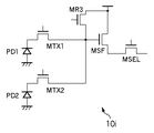
また、画素10iは、図9に示すように、2つのフォトダイオードPD1,PD2と2つの転送スイッチMTX1,MTX2とに対して、画素アンプMSF、リセットスイッチMRES及びセレクトスイッチMSELが共通化されていてもよい。この場合、一つのフォトダイオードに対する画素アンプの面積が小さくなり、結果的にフォトダイオードの開口率が向上する効果がある。また、共通化されるフォトダイオードPD1,PD2は、垂直方向に並んだものであってもよく、水平方向に並んだものであっても良い。 In the pixel 10i, as shown in FIG. 9, the pixel amplifier MSF, the reset switch MRES, and the select switch MSEL are shared by the two photodiodes PD1 and PD2 and the two transfer switches MTX1 and MTX2. Also good. In this case, the area of the pixel amplifier for one photodiode is reduced, and as a result, the aperture ratio of the photodiode is improved. Further, the photodiodes PD1 and PD2 to be shared may be arranged in the vertical direction or may be arranged in the horizontal direction.
また、選択部5jは、図10に示すように、読み出し領域から、行を選択する代わりに画素を選択しても良い。すなわち、選択部5jは、垂直走査回路VSR−A及び垂直走査回路VSR−Bに加えて、水平走査回路40jをさらに含む。水平走査回路40jは、制御線AL1,・・・を介して、制御信号φVXを画素10jのセレクトスイッチMVXへ供給する。セレクトスイッチMVXは、例えばMOSトランジスタであり、アクティブな制御信号φVXがゲートに供給された際にオンして、転送スイッチMTXから供給された信号を画素アンプMSFへ供給する。このように、選択部5jは、セレクトスイッチMSELとセレクトスイッチMVXとをともにオンさせて1つの画素を選択することで画素に対するランダムアクセスを可能とする。
Further, as illustrated in FIG. 10, the selection unit 5 j may select pixels from the readout region instead of selecting a row. That is, the selection unit 5j further includes a horizontal scanning circuit 40j in addition to the vertical scanning circuit VSR-A and the vertical scanning circuit VSR-B. The horizontal scanning circuit 40j supplies a control signal φVX to the select switch MVX of the
例えば、選択部5jは、間引いて読み出す場合、第1のフレーム期間(フレーム期間F1)に、第1の読み出し領域RR1から第1の読み出し画素群を選択する。これにより、読み出し部80は、第1のフレーム期間に、画素配列PAの全体である第1の読み出し領域RR1から第1の画素密度で信号を読み出す。第1の画素密度は、第1の読み出し画素群の画素数を第1の読み出し領域RR1の画素数で割ったものである。
For example, when thinning and reading, the selection unit 5j selects the first readout pixel group from the first readout region RR1 in the first frame period (frame period F1). As a result, the
また、選択部5jは、間引いて読み出す場合、第2のフレーム期間(フレーム期間F2又はフレーム期間F3)に、第2の読み出し領域RR2から第2の読み出し画素群を選択する。読み出し部80は、第2のフレーム期間に、画素配列PAの一部である第2の読み出し領域RR2から第1の画素密度より高い第2の画素密度で信号を読み出す。第2の画素密度は、第2の読み出し画素群の画素数を第2の読み出し領域RR1の画素数で割ったものである。
Further, when reading out by thinning, the selection unit 5j selects the second readout pixel group from the second readout region RR2 in the second frame period (frame period F2 or frame period F3). In the second frame period, the
なお、上記の説明においては、例えば行V14の画素の電荷蓄積動作をF1(n)に、例えば行V13の画素の電荷蓄積動作をF2(n)から開始させている。しかしながら、上記の説明から明らかなように、φVSR−Bの入力されるタイミングを変えることが可能であり、必ずしも上述のタイミングで電荷蓄積動作を始める必要はない。 In the above description, for example, the charge accumulation operation of the pixel in the row V14 is started from F1 (n), and the charge accumulation operation of the pixel in the row V13 is started from F2 (n), for example. However, as is apparent from the above description, the timing at which φVSR-B is input can be changed, and it is not always necessary to start the charge accumulation operation at the above timing.
さらに、この場合、制御回路60は、複数の列増幅部21,22,23,・・・のそれぞれに対応した回路要素を含んでも良く、複数の列増幅部21,22,23,・・・に対して、増幅率を画素ごとに制御しても良い。
Further, in this case, the
次に、第1実施形態に係る撮像装置を適用した撮像システムの構成の一例を、図11を用いて説明する。図11は、第1実施形態に係る撮像装置を適用した撮像システムの構成図である。 Next, an example of the configuration of an imaging system to which the imaging apparatus according to the first embodiment is applied will be described with reference to FIG. FIG. 11 is a configuration diagram of an imaging system to which the imaging apparatus according to the first embodiment is applied.
撮像システム90は、図11に示すように、主として、光学系、撮像装置1及び信号処理部を備える。光学系は、主として、シャッター91、撮影レンズ92及び絞り93を備える。信号処理部は、主として、撮像信号処理回路95、A/D変換器96、画像信号処理部97、メモリ部87、外部I/F部89、タイミング発生部98、全体制御・演算部99、記録媒体88及び記録媒体制御I/F部94を備える。なお、信号処理部は、記録媒体88を備えなくても良い。
As shown in FIG. 11, the
シャッター91は、光路上において撮影レンズ92の手前に設けられ、露出を制御する。
The
撮影レンズ92は、入射した光を屈折させて、撮像装置1の画素配列(撮像面)に被写体の像を形成する。
The
絞り93は、光路上において撮影レンズ92と撮像装置1との間に設けられ、撮影レンズ92を通過後に撮像装置1へ導かれる光の量を調節する。
The
撮像装置1は、画素配列に形成された被写体の像を画像信号に変換する。撮像装置1は、その画像信号を画素配列から読み出して出力する。
The
撮像信号処理回路95は、撮像装置1に接続されており、撮像装置1から出力された画像信号を処理する。
The imaging
A/D変換器96は、撮像信号処理回路95に接続されており、撮像信号処理回路95から出力された処理後の画像信号(アナログ信号)をデジタル信号へ変換する。
The A /
画像信号処理部97は、A/D変換器96に接続されており、A/D変換器96から出力された画像信号(デジタル信号)に各種の補正等の演算処理を行い、画像データを生成する。この画像データは、メモリ部87、外部I/F部89、全体制御・演算部99及び記録媒体制御I/F部94などへ供給される。
The image
メモリ部87は、画像信号処理部97に接続されており、画像信号処理部97から出力された画像データを記憶する。
The
表示部86は、画像信号処理部97に接続されており、画像信号処理部97から出力された画像データに応じた画像を表示する。
The
外部I/F部89は、画像信号処理部97に接続されている。これにより、画像信号処理部97から出力された画像データを、外部I/F部89を介して外部の機器(パソコン等)へ転送する。
The external I /
タイミング発生部98は、撮像装置1、撮像信号処理回路95、A/D変換器96及び画像信号処理部97に接続されている。これにより、撮像装置1、撮像信号処理回路95、A/D変換器96及び画像信号処理部97へタイミング信号を供給する。例えば、タイミング発生部98は、上述の各制御信号ΦV1、φV2、ΦG、ΦM、ΦHを撮像装置1へ供給する。そして、撮像装置1、撮像信号処理回路95、A/D変換器96及び画像信号処理部97がタイミング信号に同期して動作する。
The
全体制御・演算部99は、タイミング発生部98、画像信号処理部97、表示部86及び記録媒体制御I/F部94に接続されており、タイミング発生部98、画像信号処理部97、表示部86及び記録媒体制御I/F部94を全体的に制御する。例えば、全体制御・演算部99は、図示しない入力部に入力された指示等に基づいて、全画素読み出しモードか間引き読み出しモードかを選択して、選択したモードに応じて各部を制御する。
The overall control /
記録媒体88は、記録媒体制御I/F部94に取り外し可能に接続されている。これにより、画像信号処理部97から出力された画像データを、記録媒体制御I/F部94を介して記録媒体88へ記録する。
The recording medium 88 is detachably connected to the recording medium control I /
以上の構成により、撮像装置1において良好な画像信号が得られれば、良好な画像(画像データ)を得ることができる。
With the above configuration, if a good image signal is obtained in the
次に、撮像システム90が被写体を撮像する際の動作の一例を、図12を用いて説明する。図12は、撮像システム90が被写体を撮像する際の動作を示すフローチャートである。
Next, an example of an operation when the
ステップS1では、全体制御・演算部99が、間引き読み出しモードの撮像を開始すべきか否かを判断する。すなわち、全体制御・演算部99は、間引き読み出しモードの撮像を開始するための開始指示を入力部(図示せず)から受け取った場合、間引き読み出しモードの撮像を開始すべきと判断する。全体制御・演算部99は、開始指示を入力部から受け取らなかった場合、間引き読み出しモードの撮像を開始すべきでない(全画素読み出しモードの撮像を開始すべきである)と判断する。全体制御・演算部99は、間引き読み出しモードの撮像を開始すべきと判断した場合、処理をステップS2へ進め、間引き読み出しモードの撮像を開始すべきでないと判断した場合、処理をステップS1へ進める。
In step S1, the overall control /
ステップS2では、タイミング発生部98が、開始指示に応じて、第1の読み出し処理を行うための制御信号(ΦV1、φV2、ΦG、ΦM、ΦH)を撮像装置1へ供給する。撮像装置1は、第1の読み出し処理を行う。すなわち、選択部5は、第1の読み出し行群に含まれる行(V4,V9,V14,V19,V24)の画素に第1の蓄積時間Taで電荷蓄積動作を行わせる。第1の読み出し行群は、画素配列PAの全体から選択された領域である。読み出し部80は、フレーム期間F1(図3参照)において、第1の読み出し行群に含まれる行(V4,V9,V14,V19,V24)の画素の中から各列の画素の第1の蓄積時間Taで蓄積された信号(SA)を読み出して順次出力する。
In step S2, the
撮像信号処理回路95は、撮像装置1から出力された画像信号(SA)を処理して処理後の画像信号をA/D変換器96へ供給する。
The imaging
A/D変換器96は、撮像信号処理回路95から出力された処理後の画像信号(アナログ信号)をデジタル信号へ変換して画像信号処理部97へ出力する。
The A /
画像信号処理部97は、A/D変換器96から出力された画像信号(デジタル信号)に各種の補正等の演算処理を行い、画像データを生成する。
The image
全体制御・演算部99は、画像信号処理部97及び表示部86を制御して、画像信号処理部97が表示部86へ画像データを供給するようにし、表示部86が画像データに応じた画像を表示するようにする。また、全体制御・演算部99は、画像信号処理部97及びメモリ部87を制御して、画像信号処理部97がメモリ部87へ画像データを供給するようにし、画像信号(SA)に応じた画像データをメモリ部87が記憶するようにする。
The overall control /
ステップS3では、全体制御・演算部99が、指定処理を行うべきか否かを判断する。すなわち、入力部(図示せず)には、表示部86が表示したユーザから、注目画素領域を指定するための指定指示が入力されることがある。全体制御・演算部99は、入力部から指定指示を受け取った場合、指定処理を行うべきであると判断し、入力部から指定指示を受け取らなかった場合、指定処理を行うべきでないと判断する。全体制御・演算部99は、指定処理を行うべきであると判断した場合、処理をステップS4へ進め、指定処理を行うべきでないと判断した場合、処理をステップS7へ進める。
In step S3, the overall control /
ステップS4では、全体制御・演算部99が、指定処理を行ってその処理の結果をメモリ部87へ記憶させる。指定処理の詳細は後述する。
In step S <b> 4, the overall control /
ステップS5では、タイミング発生部98が、メモリ部87を参照して、指定処理により指定された内容にしたがって、第2の読み出し処理を行うための制御信号(ΦV1、φV2、ΦG、ΦM、ΦH)を撮像装置1へ供給する。撮像装置1は、第2の読み出し処理を行う。すなわち、選択部5は、第2の読み出し行群に含まれる行(V13〜V20)の画素に第2の蓄積時間Taaで電荷蓄積動作を行わせる。第2の読み出し行群は、画素配列PAの注目画素領域RIに対応した領域から選択された領域である。
In step S5, the
そして、読み出し部80は、フレーム期間F2(図3参照)において、第1の読み出し行群と第2の読み出し行群とに含まれる行(V14,V19)の画素の中から各列の画素の信号(SA’)を読み出して順次出力する。この信号(SA’)は、第2の蓄積時間Taaで蓄積された信号である。
Then, in the frame period F2 (see FIG. 3), the
撮像信号処理回路95は、撮像装置1から出力された画像信号(SA’)を処理して処理後の画像信号をA/D変換器96へ供給する。
The imaging
A/D変換器96は、撮像信号処理回路95から出力された処理後の画像信号(アナログ信号)をデジタル信号へ変換して画像信号処理部97へ出力する。
The A /
画像信号処理部97は、A/D変換器96から出力された画像信号(デジタル信号)に各種の補正等の演算処理を行い、画像信号(SA’)に応じた画像データを生成する。また、画像信号処理部97は、メモリ部87から画像信号(SA)に応じた画像データを取得する。画像信号処理部97は、画像信号(SA)に応じた画像データと画像信号(SA’)に応じた画像データとを合成する。
The image
全体制御・演算部99は、画像信号処理部97及び表示部86を制御して、画像信号処理部97が表示部86へ合成後の画像データを供給するようにし、表示部86が画像データに応じた画像を表示するようにする。また、全体制御・演算部99は、画像信号処理部97及びメモリ部87を制御して、画像信号処理部97がメモリ部87へ画像データを供給するようにし、合成後の画像データをメモリ部87が記憶するようにする。
The overall control /
その後、読み出し部80は、フレーム期間F3(図3参照)において、第1の読み出し行群に含まれず第2の読み出し行群に含まれる行(V13,V15〜V18,V20)の画素の中から各列の画素の信号(SB’)を読み出して順次出力する。この信号(SB’)は、第2の蓄積時間Taaで蓄積された信号である。
Thereafter, in the frame period F3 (see FIG. 3), the
撮像信号処理回路95は、撮像装置1から出力された画像信号(SB’)を処理して処理後の画像信号をA/D変換器96へ供給する。
The imaging
A/D変換器96は、撮像信号処理回路95から出力された処理後の画像信号(アナログ信号)をデジタル信号へ変換して画像信号処理部97へ出力する。
The A /
画像信号処理部97は、A/D変換器96から出力された画像信号(デジタル信号)に各種の補正等の演算処理を行い、画像信号(SB’)に応じた画像データを生成する。また、画像信号処理部97は、メモリ部87から合成後の画像データを取得する。画像信号処理部97は、当該第2の読み出し領域群RR2に含まれる行(V13,V15〜V18,V20)の画素から第1の蓄積時間Taで電荷蓄積動作を行った場合には、合成後の画像データと画像信号(SB’)に応じた画像データとをさらに合成する。
The image
全体制御・演算部99は、画像信号処理部97及び表示部86を制御して、画像信号処理部97が表示部86へ合成後の画像データを供給するようにし、表示部86が画像データに応じた画像を表示するようにする。これにより、表示部86は、注目画素領域RIに対応した部分の画像を高解像度で白とびせずに表示するとともに、画素配列PAから注目画素領域RIを除いた領域に対応した他の部分の画像を低解像度で表示する。
The overall control /
ステップS6では、全体制御・演算部99が、別の注目画素領域が存在するか否かを判断する。すなわち、全体制御・演算部99は、メモリ部87を参照し、指定された複数の領域のうち第2の読み出し領域として信号が読み出されていない領域が存在するか否かを判断する。全体制御・演算部99は、別の注目画素領域が存在すると判断する場合、処理をステップS5へ進め、別の注目画素領域が存在しないと判断する場合、処理を終了する。
In step S <b> 6, the overall control /
次に、指定処理の流れを、図13を用いて説明する。図13は、指定処理の流れの一例を示すフローチャートである。 Next, the flow of the designation process will be described with reference to FIG. FIG. 13 is a flowchart illustrating an example of the flow of the designation process.
ステップS11では、全体制御・演算部99が、画像信号処理部97及びメモリ部87を制御して、メモリ部87が記憶している複数のフレーム期間の画像データが画像信号処理部97へ供給されるようにする。これにより、画像信号処理部97は、複数のフレーム期間の画像データに基づいて、画像データが示す画像における物体の動きを検知する。この検知動作は、撮像フレーム間の画像信号の差分処理により得られた信号からノイズを除去したり、物体判別処理などにより行われる。
In
ステップS12では、全体制御・演算部99が、注目画素領域を指定する。すなわち、全体制御・演算部99は、画像信号処理部97を制御して、画像データに応じた画像において物体が存在する領域が抽出されるようにする。これにより、画像信号処理部97は、撮像装置1の画素配列PAの全体に対応した画像において、物体が存在する領域として注目画素領域RI(図3参照)に対応した領域を抽出して全体制御・演算部99へ供給する。全体制御・演算部99は、注目画素領域RIに対応した領域の情報(画素アドレスの情報等)に基づいて、注目画素領域RIを指定する。全体制御・演算部99は、指定した注目画素領域RIの情報をメモリ部87に記憶させる。
In step S12, the overall control /
ステップS13では、画像信号処理部97が、注目画素領域RIに応じた部分の画像に高輝度の部分が存在するか否かを判断する。画像信号処理部97は、高輝度の部分が存在すると判断する場合、処理をステップS14へ進め、高輝度の部分が存在しないと判断する場合、処理をステップS15へ進める。
In step S <b> 13, the image
ステップS14では、全体制御・演算部99が、第2の蓄積時間の長さを決定する。すなわち、全体制御・演算部99は、注目画素領域RIの輝度の情報を画像信号処理部97からさらに受け取る。全体制御・演算部99は、注目画素領域RIの輝度の平均値等の指標となる値を演算し、その演算結果に応じて、第2の蓄積時間の長さを決定する。全体制御・演算部99は、第2の蓄積時間の情報を指定した注目画素領域RIの情報としてメモリ部87にさらに記憶させる。
In step S14, the overall control /
ステップS15では、全体制御・演算部99が、指定する注目画素領域の情報として、予めデフォルト設定された情報に決定し、決定した情報をメモリ部87に記憶させる。
In step S <b> 15, the overall control /
なお、図13に示すステップS12では、全体制御・演算部99が、複数の注目画素領域RI,RI3を指定してもよい。例えば、全体制御・演算部99は、画像信号処理部97を制御して、注目画素領域RI3に応じた部分の画像において輝度が下限閾値以下であると判断する。
In step S12 shown in FIG. 13, the overall control /
この場合、図14に示すように、撮像装置1の垂直走査回路VSR−Aは、フレーム期間F4において、第3の読み出し領域RR3から第3の読み出し行群V2〜V7を選択する。すなわち、垂直走査回路VSR−Aは、第1の読み出し行群に含まれず第3の読み出し行群に含まれる行V2,V3,V5〜V7を順次選択する。垂直走査回路VSR−Aは、画素配列PAの全体から第3の読み出し行群に含まれる行V2,V3,V5〜V7を除く行V1,V4,V8〜V27をスキップする。垂直走査回路VSR−Aは、第1の読み出し行群に含まれず第3の読み出し行群に含まれる行(V2,V3,V5〜V7)の画素に第3の蓄積時間Tcで電荷蓄積動作を行わせる。第3の読み出し領域RR3における輝度は低いので、第3の蓄積時間Tcは、図15に示すように、第1の蓄積時間Taよりも長い。
In this case, as illustrated in FIG. 14, the vertical scanning circuit VSR-A of the
読み出し部80は、フレーム期間F4において、第1の読み出し行群に含まれず第3の読み出し行群に含まれる行(V2,V3,V5〜V7)の画素の中から各列の画素の第3の蓄積時間Tcで蓄積された信号(SC)を読み出して順次出力する。
In the frame period F4, the
このように、被写体に低輝度の部分がある場合に、その部分に対応する画素の電荷蓄積動作を行う時間を第1の蓄積時間より長くするので、画素配列PAの注目画素領域から読み出される信号のダイナミックレンジをさらに拡大することができる。 As described above, when the subject has a low-luminance portion, the time for performing the charge accumulation operation of the pixel corresponding to the portion is made longer than the first accumulation time, so that the signal read from the target pixel region of the pixel array PA The dynamic range can be further expanded.
あるいは、図13に示すステップS12では、全体制御・演算部99が、複数の注目画素領域RI,RI3aを指定してもよい。例えば、全体制御・演算部99は、画像信号処理部97を制御して、注目画素領域RI3aに応じた部分の画像において輝度が下限閾値以下であると判断する。
Alternatively, in step S12 shown in FIG. 13, the overall control /
この場合、図16に示すように、撮像装置1の垂直走査回路VSR−Aは、フレーム期間F4aにおいて、第3の読み出し領域RR3aから第3の読み出し行群V11〜V17を選択する。すなわち、垂直走査回路VSR−Aは、第1の読み出し行群に含まれず第3の読み出し行群に含まれる行V11〜V13,V15〜V17を順次選択する。垂直走査回路VSR−Aは、画素配列PAの全体から第3の読み出し行群に含まれる行V11〜V13,V15〜V17を除く行V1〜V10,V18〜V27をスキップする。垂直走査回路VSR−Aは、第1の読み出し行群に含まれず第3の読み出し行群に含まれる行(V11〜V13,V15〜V17)の画素に第3の蓄積時間Tcで電荷蓄積動作を行わせる。第3の蓄積時間Tcは、図15に示すように、第1の蓄積時間Taよりも長い。
In this case, as shown in FIG. 16, the vertical scanning circuit VSR-A of the
ここで、画素配列PAにおいて行V13,V15〜V17は、高輝度の注目画素領域RIと低輝度の注目画素領域RI3aとの両方に重なっている。この場合でも、行V13,V15〜V17の画素が第2の蓄積時間Taa及び第3の蓄積時間Tcで電荷蓄積動作を行うようにしているので、画素配列PAの注目画素領域から読み出される信号のダイナミックレンジを拡大することができる。 Here, in the pixel array PA, the rows V13 and V15 to V17 overlap both the high luminance target pixel region RI and the low luminance target pixel region RI3a. Even in this case, since the pixels in the rows V13 and V15 to V17 perform the charge accumulation operation in the second accumulation time Taa and the third accumulation time Tc, the signals read from the target pixel area of the pixel array PA The dynamic range can be expanded.
あるいは、図13に示すステップS12では、全体制御・演算部99が、複数の注目画素領域RI,RI3bを指定してもよい。ここでは、画素配列PAにおいて行V13,V15〜V17は、高輝度の注目画素領域RIと高輝度の注目画素領域RI3bとの両方に重なっている場合を考える。例えば、全体制御・演算部99は、画像信号処理部97を制御して、注目画素領域RI3bに応じた部分の画像において輝度が上限閾値以下であると判断する。
Alternatively, in step S12 shown in FIG. 13, the overall control /
この場合、垂直走査回路VSR−Aは、フレーム期間F3bにおいて、第2の読み出し行群bに含まれる行V11〜V13,V15〜V18,V20,V21を(フレーム期間F3bにおける読み出し領域として)順次選択する(図17参照)。第2の読み出し領域群RR2bは、注目画素領域RIと注目画素領域RI3bとの両方に対応した領域であり、注目画素領域RIに重なる行と注目画素領域RI3bに重なる行との和集合である。 In this case, the vertical scanning circuit VSR-A sequentially selects the rows V11 to V13, V15 to V18, V20, and V21 included in the second readout row group b (as readout regions in the frame period F3b) in the frame period F3b. (See FIG. 17). The second readout region group RR2b is a region corresponding to both the target pixel region RI and the target pixel region RI3b, and is a union of a row overlapping the target pixel region RI and a row overlapping the target pixel region RI3b.
ここで、画素配列PAにおいて行V13,V15〜V17は、高輝度の注目画素領域RIと高輝度の注目画素領域RI3bとの両方に重なっている。この場合でも、行V13,V15〜V17の画素が第2の蓄積時間Taaで電荷蓄積動作を行うようにしているので、画素配列PAの注目画素領域から読み出される信号のダイナミックレンジを拡大することができる。 Here, the rows V13 and V15 to V17 in the pixel array PA overlap both the high-luminance attention pixel region RI and the high-luminance attention pixel region RI3b. Even in this case, since the pixels in the rows V13 and V15 to V17 perform the charge accumulation operation in the second accumulation time Taa, the dynamic range of the signal read from the target pixel area of the pixel array PA can be expanded. it can.
次に、本発明の第2実施形態に係る撮像装置1kについて、図18を用いて説明する。図18は、本発明の第2実施形態に係る撮像装置1kの構成図である。以下では、第1実施形態と異なる部分を中心に説明し、同様の部分の説明を省略する。
Next, an
本発明の第2実施形態に係る撮像装置1kは、選択部5kを備える点で、第1実施形態と異なる。選択部5kは、次のように動作する点で、第1実施形態と異なる。
An
図19に示すように、前回のフレーム期間F101(n−1)において、第1の読み出し行群に含まれる行(V4,V9,V14,V19,V24)が順次選択され、各行に含まれる画素の第1の蓄積時間Taが順次開始する。 As shown in FIG. 19, in the previous frame period F101 (n−1), the rows (V4, V9, V14, V19, V24) included in the first readout row group are sequentially selected, and the pixels included in each row The first accumulation time Ta starts sequentially.
今回のフレーム期間F101(n)において、第1の読み出し行群と第2の読み出し行群とに含まれる行(V14,V19)が順次選択され、各行に含まれる画素の第2の蓄積時間Taaが順次終了する。例えば、選択部VSR−Aは、行V14の走査信号φVSR−Aに応じて、行V14の画素から信号を読み出させることで電荷蓄積動作を完了させて、行V14の第2の蓄積時間Taaを終了させる。 In the current frame period F101 (n), the rows (V14, V19) included in the first readout row group and the second readout row group are sequentially selected, and the second accumulation time Taa of the pixels included in each row is selected. Are sequentially terminated. For example, the selection unit VSR-A completes the charge accumulation operation by reading a signal from the pixel of the row V14 according to the scanning signal φVSR-A of the row V14, and the second accumulation time Taa of the row V14. End.
そして、第1の読み出し行群に含まれず第2の読み出し行群に含まれる行(V13,V15〜V18,V20)が順次選択され、各行に含まれる画素の第2の蓄積時間Taaが順次開始する(図6参照)。例えば、垂直走査回路VSR−Bは、行V13の走査信号φVSR−Bに応じて、行V13の画素をリセットし、リセットの終了により電荷蓄積動作を開始させて行V13の第2の蓄積時間Taaを開始させる。 Then, the rows (V13, V15 to V18, V20) not included in the first readout row group and included in the second readout row group are sequentially selected, and the second accumulation time Taa of the pixels included in each row starts sequentially. (See FIG. 6). For example, the vertical scanning circuit VSR-B resets the pixels in the row V13 in response to the scanning signal φVSR-B in the row V13, starts the charge accumulation operation upon completion of the reset, and performs the second accumulation time Taa in the row V13. To start.
すなわち、選択部5kは、第1実施形態におけるフレーム期間F1における動作とフレーム期間F2における動作とが、フレーム期間F101において行われるように、画素配列PAにおける各画素を駆動する。これにより、画素配列PAから信号を読み出すための時間をさらに短縮することができる。
That is, the
なお、図19では、次のサイクルに対する蓄積時間の図示が省略されている。 In FIG. 19, the accumulation time for the next cycle is not shown.
1 撮像装置
5 選択部
21等 列増幅部
30 出力部
80 読み出し部
90 撮像システム
PA 画素配列
DESCRIPTION OF
Claims (11)
前記読み出し部は、信号を間引いて読み出す場合に、第1のフレーム期間に、前記画素配列の全体である第1の読み出し領域から第1の画素密度で信号を読み出し、第2のフレーム期間に、前記画素配列の一部である第2の読み出し領域から前記第1の画素密度よりも高い第2の画素密度で信号を読み出し、前記第1の読み出し領域の画素のうち前記第1のフレーム期間に信号が読み出される画素のいずれも、前記第2の読み出し領域のうち前記第2のフレーム期間に信号が読み出される画素を含まず、
前記選択部は、信号を間引いて読み出す場合に、前記第1の読み出し領域の画素に第1の蓄積時間で電荷蓄積動作を行わせ、前記第2の読み出し領域の画素に第2の蓄積時間で電荷蓄積動作を行わせる
ことを特徴とする撮像装置。 A plurality of pixels pixel array arranged in row and column directions, a selection unit for selecting a reading area Te said pixel array odor, a reading unit for reading a signal from the read area in which the selector is selected, the a comprises Ru imaging device,
The readout unit reads out signals at a first pixel density from a first readout region, which is the entire pixel array, in a first frame period when reading out signals by thinning out, and in a second frame period, A signal is read at a second pixel density higher than the first pixel density from a second readout area that is a part of the pixel array, and the first readout period includes pixels in the first frame period. None of the pixels from which the signal is read does not include the pixels from which the signal is read in the second frame period in the second readout region,
The selection unit causes the pixels in the first readout region to perform a charge accumulation operation in a first accumulation time and reads out the signals in the second readout region in a second accumulation time when reading out signals. An imaging apparatus characterized by performing a charge accumulation operation.
ことを特徴とする請求項1に記載の撮像装置。 The selection unit causes at least some of the pixels in the first readout region to perform the accumulation operation during the second accumulation time in a period different from the charge accumulation operation during the first accumulation time. The imaging apparatus according to claim 1.
ことを特徴とする請求項1に記載の撮像装置。 The selection unit causes at least some of the pixels in the second readout region to perform the accumulation operation during the first accumulation time in a period different from the charge accumulation operation during the second accumulation time. The imaging apparatus according to claim 1.
前記読み出し部は、信号を間引いて読み出す場合、前記第1のフレーム期間に、前記第1の読み出し領域の一部の行から信号を読み出す
ことを特徴とする請求項1から3のいずれか1項に記載の撮像装置。 The selection unit selects a row in the readout region,
4. The read unit according to claim 1, wherein when the signal is read out by thinning out the signal, the signal is read from a part of the rows of the first read region in the first frame period. 5. The imaging device described in 1.
前記読み出し部は、信号を間引いて読み出す場合、前記第1のフレーム期間に、前記第1の読み出し領域の一部の行かつ一部の列の画素から信号を読み出す
ことを特徴とする請求項1から3のいずれか1項に記載の撮像装置。 The selection unit selects a pixel in the readout region,
The reading unit reads signals from pixels in a part of rows and a part of columns of the first readout region in the first frame period when the signals are thinned out and read out. 4. The imaging device according to any one of items 1 to 3.
各列の画素の信号をそれぞれ増幅する複数の列増幅部と、
前記複数の列増幅部が増幅した信号を順次出力する出力部と、
を含み、
前記複数の列増幅部のそれぞれは、信号を増幅する増幅率が行ごとに制御される
ことを特徴とする請求項4に記載の撮像装置。 The reading unit
A plurality of column amplification units for amplifying the signals of the pixels in each column;
An output unit for sequentially outputting signals amplified by the plurality of column amplification units;
Including
The imaging apparatus according to claim 4, wherein an amplification factor for amplifying a signal is controlled for each row in each of the plurality of column amplification units.
各列の画素の信号をそれぞれ増幅する複数の列増幅部と、
前記複数の列増幅部が増幅した信号を順次出力する出力部と、
を含み、
前記複数の列増幅部のそれぞれは、信号を増幅する増幅率が画素ごとに制御される
ことを特徴とする請求項5に記載の撮像装置。 The reading unit
A plurality of column amplification units for amplifying the signals of the pixels in each column;
An output unit for sequentially outputting signals amplified by the plurality of column amplification units;
Including
The imaging apparatus according to claim 5, wherein an amplification factor for amplifying a signal of each of the plurality of column amplification units is controlled for each pixel.
ことを特徴とする請求項1から7のいずれか1項に記載の撮像装置。 The selection unit causes a pixel that is included in the first readout region and not included in the second readout region to perform a charge accumulation operation in the first accumulation time, and at least a part of the second readout region 8. The charge storage operation during the first storage time and the charge storage operation during the second storage time are performed in different periods by the pixels included in the pixel. 8. The imaging device described in 1.
ことを特徴とする請求項1から8のいずれか1項に記載の撮像装置。The image pickup apparatus according to claim 1, wherein the image pickup apparatus is an image pickup apparatus.
前記撮像装置の撮像面へ像を形成する光学系と、
前記撮像装置から出力された信号を処理して画像データを生成する信号処理部と、を備え、
前記信号処理部は、前記第1の読み出し領域から読み出された信号の輝度に基づいて、前記第1の蓄積時間を決定し、前記第1の読み出し領域の画素に前記第1の蓄積時間で電荷蓄積動作を行わせるように、前記撮像装置の前記選択部を制御し、前記第2の読み出し領域から読み出された信号の輝度に基づいて、前記第2の蓄積時間を決定し、前記第2の読み出し領域の画素に前記第2の蓄積時間で電荷蓄積動作を行わせるように、前記撮像装置の前記選択部を制御する
ことを特徴とする撮像システム。 The imaging device according to any one of claims 1 to 9 ,
An optical system for forming an image on the imaging surface of the imaging device;
A signal processing unit that processes the signal output from the imaging device and generates image data,
The signal processing unit determines the first accumulation time based on the luminance of the signal read from the first readout area, and the pixel in the first readout area is determined based on the first accumulation time. The selection unit of the imaging device is controlled to perform a charge accumulation operation, the second accumulation time is determined based on the luminance of the signal read from the second readout region, and the second accumulation time is determined. 2. The imaging system according to claim 1, wherein the selection unit of the imaging apparatus is controlled to cause a pixel in two readout regions to perform a charge accumulation operation in the second accumulation time.
前記画素配列の全体である第1の読み出し領域から第1の画素密度で信号を読み出す第1の動作と、A first operation of reading a signal at a first pixel density from a first readout region that is the entire pixel array;
前記画素配列の一部である第2の読み出し領域から前記第1の画素密度よりも高い第2の画素密度で信号を読み出す第2の動作と、を含み、A second operation of reading a signal at a second pixel density higher than the first pixel density from a second readout region that is a part of the pixel array,
前記第1の読み出し領域の画素のうち前記第1のフレーム期間に信号が読み出される画素のいずれも、前記第2の読み出し領域のうち前記第2のフレーム期間に信号が読み出される画素を含まず、None of the pixels of the first readout region from which signals are read during the first frame period does not include pixels of the second readout region from which signals are read during the second frame period,
前記第1の読み出し領域の画素のうち前記第1の動作で信号を読み出すべき画素には第1の蓄積時間で電荷蓄積動作を行わせ、前記第2の読み出し領域の画素のうち前記第2の動作で信号を読み出すべき画素には第2の蓄積時間で電荷蓄積動作を行わせる、Among the pixels in the first readout region, the pixels from which signals are to be read out in the first operation are caused to perform a charge accumulation operation in a first accumulation time, and among the pixels in the second readout region, the second The pixel that is to read the signal by the operation is caused to perform the charge accumulation operation in the second accumulation time.
ことを特徴とする撮像装置の動作方法。An operation method of an imaging apparatus characterized by the above.
Priority Applications (2)
| Application Number | Priority Date | Filing Date | Title |
|---|---|---|---|
| JP2007190118A JP5063234B2 (en) | 2007-07-20 | 2007-07-20 | IMAGING DEVICE, IMAGING SYSTEM, AND OPERATION METHOD OF IMAGING DEVICE |
| US12/167,436 US8189086B2 (en) | 2007-07-20 | 2008-07-03 | Image sensing apparatus and image capturing system that performs a thinning-out readout |
Applications Claiming Priority (1)
| Application Number | Priority Date | Filing Date | Title |
|---|---|---|---|
| JP2007190118A JP5063234B2 (en) | 2007-07-20 | 2007-07-20 | IMAGING DEVICE, IMAGING SYSTEM, AND OPERATION METHOD OF IMAGING DEVICE |
Publications (3)
| Publication Number | Publication Date |
|---|---|
| JP2009027559A JP2009027559A (en) | 2009-02-05 |
| JP2009027559A5 JP2009027559A5 (en) | 2010-08-26 |
| JP5063234B2 true JP5063234B2 (en) | 2012-10-31 |
Family
ID=40264525
Family Applications (1)
| Application Number | Title | Priority Date | Filing Date |
|---|---|---|---|
| JP2007190118A Active JP5063234B2 (en) | 2007-07-20 | 2007-07-20 | IMAGING DEVICE, IMAGING SYSTEM, AND OPERATION METHOD OF IMAGING DEVICE |
Country Status (2)
| Country | Link |
|---|---|
| US (1) | US8189086B2 (en) |
| JP (1) | JP5063234B2 (en) |
Cited By (1)
| Publication number | Priority date | Publication date | Assignee | Title |
|---|---|---|---|---|
| US11252348B2 (en) | 2018-04-27 | 2022-02-15 | Sony Semiconductor Solutions Corporation | Imaging device and driving method of imaging device |
Families Citing this family (56)
| Publication number | Priority date | Publication date | Assignee | Title |
|---|---|---|---|---|
| JP5106052B2 (en) * | 2007-11-08 | 2012-12-26 | キヤノン株式会社 | Solid-state imaging device, imaging system, and solid-state imaging device driving method |
| US8390710B2 (en) | 2007-12-19 | 2013-03-05 | Canon Kabushiki Kaisha | Image pickup system, method for driving image pickup elements, and recording medium |
| JP5288823B2 (en) * | 2008-02-18 | 2013-09-11 | キヤノン株式会社 | Photoelectric conversion device and method for manufacturing photoelectric conversion device |
| JP5407391B2 (en) | 2008-03-04 | 2014-02-05 | 株式会社リコー | Optical scanning image forming apparatus |
| JP5188292B2 (en) * | 2008-06-30 | 2013-04-24 | キヤノン株式会社 | Imaging system and driving method of imaging system |
| US8970707B2 (en) * | 2008-12-17 | 2015-03-03 | Sony Computer Entertainment Inc. | Compensating for blooming of a shape in an image |
| JP5315039B2 (en) * | 2008-12-19 | 2013-10-16 | キヤノン株式会社 | Imaging sensor, imaging system, and driving method of imaging sensor |
| US8218068B2 (en) * | 2009-04-01 | 2012-07-10 | Omnivision Technologies, Inc. | Exposing pixel groups in producing digital images |
| JP5214538B2 (en) * | 2009-05-25 | 2013-06-19 | オリンパス株式会社 | Image acquisition apparatus, image composition method, and microscope system |
| JP5404194B2 (en) * | 2009-06-05 | 2014-01-29 | キヤノン株式会社 | Solid-state imaging device, imaging system, and solid-state imaging device driving method |
| JP5219962B2 (en) * | 2009-08-13 | 2013-06-26 | キヤノン株式会社 | Solid-state imaging device, driving method thereof, and imaging system |
| JP5482154B2 (en) * | 2009-12-02 | 2014-04-23 | セイコーエプソン株式会社 | Imaging apparatus, imaging method, and imaging program |
| JP5593975B2 (en) * | 2010-08-30 | 2014-09-24 | 富士通セミコンダクター株式会社 | Image processing apparatus, image processing method, and scheduling apparatus |
| US8928789B2 (en) | 2010-09-30 | 2015-01-06 | Canon Kabushiki Kaisha | Solid-state imaging apparatus |
| JP5610961B2 (en) | 2010-09-30 | 2014-10-22 | キヤノン株式会社 | Solid-state imaging device and driving method of solid-state imaging device |
| JP2012235332A (en) * | 2011-05-02 | 2012-11-29 | Sony Corp | Imaging apparatus, imaging apparatus control method and program |
| JP2013005017A (en) * | 2011-06-13 | 2013-01-07 | Sony Corp | Image pickup apparatus, image pickup apparatus control method, and program |
| JP5808162B2 (en) | 2011-06-23 | 2015-11-10 | キヤノン株式会社 | Imaging device, imaging apparatus, and driving method of imaging device |
| JP6039897B2 (en) * | 2011-12-02 | 2016-12-07 | 東レ・ファインケミカル株式会社 | Manufacturing method of electret synthetic fiber sheet |
| JP5624228B2 (en) * | 2011-12-27 | 2014-11-12 | 富士フイルム株式会社 | IMAGING DEVICE, IMAGING DEVICE CONTROL METHOD, AND CONTROL PROGRAM |
| JP5956755B2 (en) | 2012-01-06 | 2016-07-27 | キヤノン株式会社 | Solid-state imaging device and imaging system |
| JP5893573B2 (en) | 2012-02-09 | 2016-03-23 | キヤノン株式会社 | Solid-state imaging device |
| JP5893550B2 (en) | 2012-04-12 | 2016-03-23 | キヤノン株式会社 | Imaging apparatus and imaging system |
| JP6222915B2 (en) * | 2012-10-29 | 2017-11-01 | キヤノン株式会社 | Imaging device, driving method of imaging device, program, and recording medium |
| JP2014197832A (en) | 2013-03-07 | 2014-10-16 | キヤノン株式会社 | Image-capturing device and drive method thereof |
| FR3004570B1 (en) * | 2013-04-11 | 2016-09-02 | Aldebaran Robotics | METHOD OF ESTIMATING THE ANGULAR DEVIATION OF A MOBILE ELEMENT RELATING TO A REFERENCE DIRECTION |
| JP6274788B2 (en) | 2013-08-28 | 2018-02-07 | キヤノン株式会社 | Imaging apparatus, imaging system, and driving method of imaging apparatus |
| JP6230395B2 (en) | 2013-12-06 | 2017-11-15 | キヤノン株式会社 | Imaging apparatus and driving method thereof |
| JP6338385B2 (en) * | 2014-01-31 | 2018-06-06 | キヤノン株式会社 | IMAGING DEVICE, IMAGING SYSTEM, IMAGING DEVICE CONTROL METHOD, AND IMAGING DEVICE HAVING IMAGING DEVICE |
| JP6336286B2 (en) * | 2014-01-31 | 2018-06-06 | キヤノン株式会社 | IMAGING DEVICE, IMAGING SYSTEM, IMAGING DEVICE CONTROL METHOD, AND IMAGING DEVICE HAVING IMAGING DEVICE |
| EP2942941B1 (en) * | 2014-05-08 | 2016-04-27 | Axis AB | Method and apparatus for determining a need for a change in a pixel density requirement due to changing light conditions |
| JP6442261B2 (en) * | 2014-06-05 | 2018-12-19 | キヤノン株式会社 | Image pickup device, image pickup apparatus, and control method thereof |
| JP6389685B2 (en) | 2014-07-30 | 2018-09-12 | キヤノン株式会社 | Imaging apparatus and imaging system |
| CN104363381B (en) * | 2014-10-15 | 2018-03-02 | 北京智谷睿拓技术服务有限公司 | IMAQ control method and device |
| US9979916B2 (en) | 2014-11-21 | 2018-05-22 | Canon Kabushiki Kaisha | Imaging apparatus and imaging system |
| US9912886B2 (en) | 2014-12-17 | 2018-03-06 | Canon Kabushiki Kaisha | Image capturing apparatus and driving method of image sensor |
| JP6525694B2 (en) * | 2015-04-08 | 2019-06-05 | キヤノン株式会社 | Imaging device, imaging system, and driving method of imaging device |
| US9900539B2 (en) | 2015-09-10 | 2018-02-20 | Canon Kabushiki Kaisha | Solid-state image pickup element, and image pickup system |
| JP6674219B2 (en) | 2015-10-01 | 2020-04-01 | キヤノン株式会社 | Solid-state imaging device and imaging system |
| JP6700731B2 (en) * | 2015-11-13 | 2020-05-27 | キヤノン株式会社 | Projection device and projection system |
| US20170332000A1 (en) * | 2016-05-10 | 2017-11-16 | Lytro, Inc. | High dynamic range light-field imaging |
| US10319765B2 (en) | 2016-07-01 | 2019-06-11 | Canon Kabushiki Kaisha | Imaging device having an effective pixel region, an optical black region and a dummy region each with pixels including a photoelectric converter |
| JP6929671B2 (en) | 2017-03-17 | 2021-09-01 | キヤノン株式会社 | Imaging device and imaging system |
| JP6929114B2 (en) | 2017-04-24 | 2021-09-01 | キヤノン株式会社 | Photoelectric conversion device and imaging system |
| US10582143B2 (en) * | 2017-05-29 | 2020-03-03 | Imec Vzw | Programmable state machine |
| US10411798B2 (en) * | 2017-07-13 | 2019-09-10 | Qualcomm Incorporated | Power optimized VLC signal processing with efficient handling of ISP/VFE |
| JP7150469B2 (en) | 2018-05-17 | 2022-10-11 | キヤノン株式会社 | Imaging device and imaging system |
| WO2019225122A1 (en) * | 2018-05-25 | 2019-11-28 | ソニーセミコンダクタソリューションズ株式会社 | Solid-state imaging apparatus and electronic device equipped with solid-state imaging apparatus |
| US11606500B2 (en) * | 2018-12-06 | 2023-03-14 | Sony Semiconductor Solutions Corporation | Reception apparatus and transmission apparatus |
| US10855896B1 (en) | 2018-12-13 | 2020-12-01 | Facebook Technologies, Llc | Depth determination using time-of-flight and camera assembly with augmented pixels |
| US10791286B2 (en) | 2018-12-13 | 2020-09-29 | Facebook Technologies, Llc | Differentiated imaging using camera assembly with augmented pixels |
| US10791282B2 (en) * | 2018-12-13 | 2020-09-29 | Fenwick & West LLP | High dynamic range camera assembly with augmented pixels |
| JP7204480B2 (en) | 2018-12-27 | 2023-01-16 | キヤノン株式会社 | IMAGING DEVICE, IMAGING SYSTEM, MOVING OBJECT, AND IMAGING DEVICE CONTROL METHOD |
| KR20210014021A (en) * | 2019-07-29 | 2021-02-08 | 삼성전자주식회사 | Image sensor, image processing system and operating method thereof |
| US10902623B1 (en) | 2019-11-19 | 2021-01-26 | Facebook Technologies, Llc | Three-dimensional imaging with spatial and temporal coding for depth camera assembly |
| US11194160B1 (en) | 2020-01-21 | 2021-12-07 | Facebook Technologies, Llc | High frame rate reconstruction with N-tap camera sensor |
Family Cites Families (23)
| Publication number | Priority date | Publication date | Assignee | Title |
|---|---|---|---|---|
| US4731665A (en) | 1984-12-28 | 1988-03-15 | Canon Kabushiki Kaisha | Image sensing apparatus with read-out of selected combinations of lines |
| EP0277016B1 (en) | 1987-01-29 | 1998-04-15 | Canon Kabushiki Kaisha | Photoelectric conversion apparatus |
| US4959723A (en) | 1987-11-06 | 1990-09-25 | Canon Kabushiki Kaisha | Solid state image pickup apparatus having multi-phase scanning pulse to read out accumulated signal |
| US5146339A (en) | 1989-11-21 | 1992-09-08 | Canon Kabushiki Kaisha | Photoelectric converting apparatus employing Darlington transistor readout |
| CA2056087C (en) | 1990-11-27 | 1998-01-27 | Masakazu Morishita | Photoelectric converting device and information processing apparatus employing the same |
| US5452004A (en) * | 1993-06-17 | 1995-09-19 | Litton Systems, Inc. | Focal plane array imaging device with random access architecture |
| JPH09214836A (en) | 1996-02-07 | 1997-08-15 | Olympus Optical Co Ltd | Image pickup device |
| US6906751B1 (en) * | 1998-07-22 | 2005-06-14 | Minolta Co., Ltd. | Digital camera and control method thereof |
| JP4403635B2 (en) | 2000-05-31 | 2010-01-27 | パナソニック株式会社 | Dynamic range expansion camera |
| JP4503878B2 (en) * | 2001-04-27 | 2010-07-14 | オリンパス株式会社 | Imaging apparatus and imaging method |
| JP4019409B2 (en) | 2001-11-02 | 2007-12-12 | ソニー株式会社 | Solid-state image sensor |
| JP2005175626A (en) * | 2003-12-08 | 2005-06-30 | Micron Technology Inc | Wide dynamic range operation for imaging |
| JP4426885B2 (en) * | 2004-03-23 | 2010-03-03 | オリンパス株式会社 | Solid-state imaging device |
| JP2006121151A (en) * | 2004-10-19 | 2006-05-11 | Sony Corp | Signal processing method, signal processing apparatus and physical information acquiring apparatus |
| WO2006048987A1 (en) * | 2004-11-02 | 2006-05-11 | Japan Science And Technology Agency | Image pickup device, and its signal reading method |
| US8045047B2 (en) * | 2005-06-23 | 2011-10-25 | Nokia Corporation | Method and apparatus for digital image processing of an image having different scaling rates |
| JP2007013292A (en) * | 2005-06-28 | 2007-01-18 | Olympus Corp | Imaging apparatus |
| JP4756960B2 (en) * | 2005-09-02 | 2011-08-24 | キヤノン株式会社 | Imaging apparatus, control method therefor, computer program, and storage medium |
| JP3996631B2 (en) * | 2005-09-09 | 2007-10-24 | 松下電器産業株式会社 | Image processing method, image recording method, image processing apparatus, and image file format |
| JP4888081B2 (en) * | 2006-01-23 | 2012-02-29 | セイコーエプソン株式会社 | Imaging apparatus, imaging method, imaging system, and image processing apparatus |
| JP4018727B2 (en) * | 2006-02-14 | 2007-12-05 | キヤノン株式会社 | IMAGING DEVICE, ITS CONTROL METHOD, PROGRAM, AND STORAGE MEDIUM |
| JP5188080B2 (en) * | 2007-03-06 | 2013-04-24 | キヤノン株式会社 | Imaging device, driving method of imaging device, and readout device |
| US8441535B2 (en) * | 2008-03-05 | 2013-05-14 | Omnivision Technologies, Inc. | System and method for independent image sensor parameter control in regions of interest |
-
2007
- 2007-07-20 JP JP2007190118A patent/JP5063234B2/en active Active
-
2008
- 2008-07-03 US US12/167,436 patent/US8189086B2/en active Active
Cited By (1)
| Publication number | Priority date | Publication date | Assignee | Title |
|---|---|---|---|---|
| US11252348B2 (en) | 2018-04-27 | 2022-02-15 | Sony Semiconductor Solutions Corporation | Imaging device and driving method of imaging device |
Also Published As
| Publication number | Publication date |
|---|---|
| US20090021621A1 (en) | 2009-01-22 |
| US8189086B2 (en) | 2012-05-29 |
| JP2009027559A (en) | 2009-02-05 |
Similar Documents
| Publication | Publication Date | Title |
|---|---|---|
| JP5063234B2 (en) | IMAGING DEVICE, IMAGING SYSTEM, AND OPERATION METHOD OF IMAGING DEVICE | |
| JP5188080B2 (en) | Imaging device, driving method of imaging device, and readout device | |
| JP5226552B2 (en) | Imaging device | |
| JP4208904B2 (en) | Imaging apparatus, control method therefor, and imaging system | |
| JP5888914B2 (en) | Imaging apparatus and control method thereof | |
| JP5111140B2 (en) | Solid-state imaging device driving method, solid-state imaging device, and imaging system | |
| US7697038B2 (en) | Imaging apparatus and method for controlling thereof and imaging system | |
| US20100321532A1 (en) | Solid-state imaging device, imaging system, and method of driving solid-state imaging device | |
| US7907193B2 (en) | Image capturing apparatus | |
| JP5101946B2 (en) | Imaging apparatus and imaging system | |
| JP6099904B2 (en) | Imaging device | |
| JP2015115660A5 (en) | IMAGING DEVICE, ITS CONTROL METHOD, AND IMAGING ELEMENT | |
| CN109474781B (en) | Image pickup apparatus, control method for image pickup apparatus, and recording medium | |
| JPWO2018181582A1 (en) | Imaging device, focus adjustment device, and imaging device | |
| JP7332302B2 (en) | Imaging device and its control method | |
| JP2007124542A (en) | Imaging apparatus, and control method, program and recording medium thereof | |
| JP2006033381A (en) | Imaging device and control method | |
| JP6929106B2 (en) | Imaging device and control method of imaging device | |
| JP2009124238A (en) | Imaging device and its flicker detecting method | |
| JP2021122131A (en) | Imaging element and imaging device | |
| JP2007135073A (en) | Solid state imaging device | |
| JP2005328213A (en) | Solid state imaging device and its driving method | |
| JP2010171856A (en) | Imaging apparatus | |
| JP5067843B2 (en) | Imaging device | |
| JP5106056B2 (en) | Imaging apparatus and flicker detection method thereof |
Legal Events
| Date | Code | Title | Description |
|---|---|---|---|
| A521 | Request for written amendment filed |
Free format text: JAPANESE INTERMEDIATE CODE: A523 Effective date: 20100709 |
|
| A621 | Written request for application examination |
Free format text: JAPANESE INTERMEDIATE CODE: A621 Effective date: 20100709 |
|
| A977 | Report on retrieval |
Free format text: JAPANESE INTERMEDIATE CODE: A971007 Effective date: 20120117 |
|
| A131 | Notification of reasons for refusal |
Free format text: JAPANESE INTERMEDIATE CODE: A131 Effective date: 20120123 |
|
| A521 | Request for written amendment filed |
Free format text: JAPANESE INTERMEDIATE CODE: A523 Effective date: 20120306 |
|
| TRDD | Decision of grant or rejection written | ||
| A01 | Written decision to grant a patent or to grant a registration (utility model) |
Free format text: JAPANESE INTERMEDIATE CODE: A01 Effective date: 20120709 |
|
| A01 | Written decision to grant a patent or to grant a registration (utility model) |
Free format text: JAPANESE INTERMEDIATE CODE: A01 |
|
| A61 | First payment of annual fees (during grant procedure) |
Free format text: JAPANESE INTERMEDIATE CODE: A61 Effective date: 20120807 |
|
| R151 | Written notification of patent or utility model registration |
Ref document number: 5063234 Country of ref document: JP Free format text: JAPANESE INTERMEDIATE CODE: R151 |
|
| FPAY | Renewal fee payment (event date is renewal date of database) |
Free format text: PAYMENT UNTIL: 20150817 Year of fee payment: 3 |