JP7204480B2 - IMAGING DEVICE, IMAGING SYSTEM, MOVING OBJECT, AND IMAGING DEVICE CONTROL METHOD - Google Patents
IMAGING DEVICE, IMAGING SYSTEM, MOVING OBJECT, AND IMAGING DEVICE CONTROL METHOD Download PDFInfo
- Publication number
- JP7204480B2 JP7204480B2 JP2018245447A JP2018245447A JP7204480B2 JP 7204480 B2 JP7204480 B2 JP 7204480B2 JP 2018245447 A JP2018245447 A JP 2018245447A JP 2018245447 A JP2018245447 A JP 2018245447A JP 7204480 B2 JP7204480 B2 JP 7204480B2
- Authority
- JP
- Japan
- Prior art keywords
- image data
- unit
- charge
- photoelectric conversion
- exposure
- Prior art date
- Legal status (The legal status is an assumption and is not a legal conclusion. Google has not performed a legal analysis and makes no representation as to the accuracy of the status listed.)
- Active
Links
- 238000003384 imaging method Methods 0.000 title claims description 126
- 238000000034 method Methods 0.000 title claims description 28
- 238000006243 chemical reaction Methods 0.000 claims description 70
- 238000012546 transfer Methods 0.000 claims description 69
- 238000012545 processing Methods 0.000 claims description 49
- 230000006835 compression Effects 0.000 claims description 44
- 238000007906 compression Methods 0.000 claims description 44
- 230000002194 synthesizing effect Effects 0.000 claims description 13
- 230000004397 blinking Effects 0.000 claims description 8
- 238000010586 diagram Methods 0.000 description 29
- 238000005070 sampling Methods 0.000 description 24
- 230000000052 comparative effect Effects 0.000 description 17
- 238000001514 detection method Methods 0.000 description 13
- 101001092910 Homo sapiens Serum amyloid P-component Proteins 0.000 description 12
- 102100036202 Serum amyloid P-component Human genes 0.000 description 12
- 230000015572 biosynthetic process Effects 0.000 description 11
- 238000009792 diffusion process Methods 0.000 description 11
- 230000000694 effects Effects 0.000 description 11
- 238000003786 synthesis reaction Methods 0.000 description 11
- 238000009825 accumulation Methods 0.000 description 10
- 230000003321 amplification Effects 0.000 description 10
- 230000000875 corresponding effect Effects 0.000 description 10
- 238000003199 nucleic acid amplification method Methods 0.000 description 10
- 208000009989 Posterior Leukoencephalopathy Syndrome Diseases 0.000 description 7
- 102100032752 C-reactive protein Human genes 0.000 description 6
- 101000942118 Homo sapiens C-reactive protein Proteins 0.000 description 6
- 101000920800 Homo sapiens Endoplasmic reticulum-Golgi intermediate compartment protein 2 Proteins 0.000 description 6
- 101000583156 Homo sapiens Pituitary homeobox 1 Proteins 0.000 description 6
- KJWMGLBVDNMNQW-VWTMXFPPSA-N Pectenotoxin 1 Chemical compound O[C@@H]1[C@H](C)CCO[C@]1(O)[C@H]1O[C@@H]2/C=C/C(/C)=C/[C@H](C)C[C@](C)(O3)CC[C@@H]3[C@](O3)(O4)CC[C@@]3(CO)C[C@@H]4[C@@H](O3)C(=O)C[C@]3(C)[C@@H](O)[C@@H](O3)CC[C@@]3(O3)CCC[C@H]3[C@@H](C)C(=O)O[C@@H]2C1 KJWMGLBVDNMNQW-VWTMXFPPSA-N 0.000 description 6
- 102220035924 rs515726219 Human genes 0.000 description 6
- 230000006870 function Effects 0.000 description 5
- 230000001276 controlling effect Effects 0.000 description 4
- 238000005286 illumination Methods 0.000 description 4
- 238000012935 Averaging Methods 0.000 description 3
- 238000005259 measurement Methods 0.000 description 3
- 230000003071 parasitic effect Effects 0.000 description 3
- 102200106455 rs2072799 Human genes 0.000 description 3
- 101000622137 Homo sapiens P-selectin Proteins 0.000 description 2
- 102100023472 P-selectin Human genes 0.000 description 2
- 238000012937 correction Methods 0.000 description 2
- 230000007547 defect Effects 0.000 description 2
- 230000006866 deterioration Effects 0.000 description 2
- 230000003287 optical effect Effects 0.000 description 2
- 239000004065 semiconductor Substances 0.000 description 2
- 101001094051 Homo sapiens Prestin Proteins 0.000 description 1
- 102100035276 Prestin Human genes 0.000 description 1
- 230000004888 barrier function Effects 0.000 description 1
- 239000002131 composite material Substances 0.000 description 1
- 230000002596 correlated effect Effects 0.000 description 1
- 238000007599 discharging Methods 0.000 description 1
- 238000005516 engineering process Methods 0.000 description 1
- 239000004973 liquid crystal related substance Substances 0.000 description 1
- 239000000203 mixture Substances 0.000 description 1
- 230000008447 perception Effects 0.000 description 1
- 238000005096 rolling process Methods 0.000 description 1
- 239000000758 substrate Substances 0.000 description 1
Images


Classifications
-
- H—ELECTRICITY
- H04—ELECTRIC COMMUNICATION TECHNIQUE
- H04N—PICTORIAL COMMUNICATION, e.g. TELEVISION
- H04N23/00—Cameras or camera modules comprising electronic image sensors; Control thereof
- H04N23/70—Circuitry for compensating brightness variation in the scene
- H04N23/73—Circuitry for compensating brightness variation in the scene by influencing the exposure time
-
- H—ELECTRICITY
- H04—ELECTRIC COMMUNICATION TECHNIQUE
- H04N—PICTORIAL COMMUNICATION, e.g. TELEVISION
- H04N23/00—Cameras or camera modules comprising electronic image sensors; Control thereof
- H04N23/70—Circuitry for compensating brightness variation in the scene
- H04N23/745—Detection of flicker frequency or suppression of flicker wherein the flicker is caused by illumination, e.g. due to fluorescent tube illumination or pulsed LED illumination
-
- H—ELECTRICITY
- H04—ELECTRIC COMMUNICATION TECHNIQUE
- H04N—PICTORIAL COMMUNICATION, e.g. TELEVISION
- H04N23/00—Cameras or camera modules comprising electronic image sensors; Control thereof
- H04N23/70—Circuitry for compensating brightness variation in the scene
- H04N23/71—Circuitry for evaluating the brightness variation
-
- H—ELECTRICITY
- H04—ELECTRIC COMMUNICATION TECHNIQUE
- H04N—PICTORIAL COMMUNICATION, e.g. TELEVISION
- H04N23/00—Cameras or camera modules comprising electronic image sensors; Control thereof
- H04N23/70—Circuitry for compensating brightness variation in the scene
- H04N23/741—Circuitry for compensating brightness variation in the scene by increasing the dynamic range of the image compared to the dynamic range of the electronic image sensors
-
- H—ELECTRICITY
- H04—ELECTRIC COMMUNICATION TECHNIQUE
- H04N—PICTORIAL COMMUNICATION, e.g. TELEVISION
- H04N23/00—Cameras or camera modules comprising electronic image sensors; Control thereof
- H04N23/95—Computational photography systems, e.g. light-field imaging systems
- H04N23/951—Computational photography systems, e.g. light-field imaging systems by using two or more images to influence resolution, frame rate or aspect ratio
-
- H—ELECTRICITY
- H04—ELECTRIC COMMUNICATION TECHNIQUE
- H04N—PICTORIAL COMMUNICATION, e.g. TELEVISION
- H04N25/00—Circuitry of solid-state image sensors [SSIS]; Control thereof
- H04N25/50—Control of the SSIS exposure
- H04N25/57—Control of the dynamic range
- H04N25/58—Control of the dynamic range involving two or more exposures
- H04N25/587—Control of the dynamic range involving two or more exposures acquired sequentially, e.g. using the combination of odd and even image fields
- H04N25/589—Control of the dynamic range involving two or more exposures acquired sequentially, e.g. using the combination of odd and even image fields with different integration times, e.g. short and long exposures
-
- H—ELECTRICITY
- H04—ELECTRIC COMMUNICATION TECHNIQUE
- H04N—PICTORIAL COMMUNICATION, e.g. TELEVISION
- H04N25/00—Circuitry of solid-state image sensors [SSIS]; Control thereof
- H04N25/70—SSIS architectures; Circuits associated therewith
- H04N25/76—Addressed sensors, e.g. MOS or CMOS sensors
- H04N25/77—Pixel circuitry, e.g. memories, A/D converters, pixel amplifiers, shared circuits or shared components
-
- H—ELECTRICITY
- H04—ELECTRIC COMMUNICATION TECHNIQUE
- H04N—PICTORIAL COMMUNICATION, e.g. TELEVISION
- H04N25/00—Circuitry of solid-state image sensors [SSIS]; Control thereof
- H04N25/70—SSIS architectures; Circuits associated therewith
- H04N25/76—Addressed sensors, e.g. MOS or CMOS sensors
- H04N25/78—Readout circuits for addressed sensors, e.g. output amplifiers or A/D converters
Description
本発明は、撮像装置、撮像システム、移動体及び撮像装置の制御方法に関する。 The present invention relates to an imaging device, an imaging system, a moving body, and a control method for an imaging device.
特許文献1には、互いに異なる露光量で複数の画像を撮影し、当該複数の画像を合成することによりダイナミックレンジが拡張された画像を生成することができる撮像装置が開示されている。 Japanese Unexamined Patent Application Publication No. 2002-200000 discloses an imaging apparatus capable of capturing a plurality of images with mutually different exposure amounts and synthesizing the plurality of images to generate an image with an extended dynamic range.
特許文献1に記載されているような露光時間の異なる複数の画像を撮影することができる撮像装置において、撮影された画像の明るさが光源の点滅に応じて変動するフリッカ現象が問題となり得る。
In an imaging apparatus capable of capturing a plurality of images with different exposure times as described in
本発明は、露光時間の異なる複数の画像を取得する場合において、画質を維持しつつフリッカ現象の影響を低減することが可能な撮像装置、撮像システム、移動体及び撮像装置の制御方法を提供することを目的とする。 The present invention provides an imaging device, an imaging system, a moving object, and a control method for the imaging device that can reduce the influence of flicker while maintaining image quality when acquiring a plurality of images with different exposure times. for the purpose.
本発明の一観点によれば、入射光に応じた電荷を生成する光電変換部と、前記電荷を保持する電荷保持部と、前記光電変換部から前記電荷保持部に前記電荷を転送する電荷転送部と、前記電荷保持部に転送された電荷に基づく信号を出力する出力部と、を有する撮像装置によって取得されたデータを処理する装置であって、第1露光時間において前記光電変換部で生じた電荷に基づく第1画像データを取得する第1取得部と、前記電荷転送部によって前記光電変換部から前記電荷保持部に複数回にわたって転送された電荷の露光時間の合計であり、かつ前記第1露光時間よりも長い第2露光時間において前記光電変換部で生じた電荷に基づく第2画像データを取得する第2取得部と、前記第2画像データの階調値を減少させて第3画像データを生成する圧縮部と、前記第1画像データと前記第3画像データとを合成して、拡張されたダイナミックレンジを有する第4画像データを生成する画像合成部と、を備えることを特徴とする装置が提供される。 According to one aspect of the present invention, a photoelectric conversion portion that generates charges according to incident light, a charge holding portion that holds the charges, and a charge transfer that transfers the charges from the photoelectric conversion portion to the charge holding portion. and an output unit for outputting a signal based on the charge transferred to the charge holding unit, the device processing data acquired by an imaging device, wherein the photoelectric conversion unit generates data during a first exposure time. and the exposure time of the charges transferred from the photoelectric conversion unit to the charge holding unit a plurality of times by the charge transfer unit, and the exposure time of the charges, and a second acquisition unit that acquires second image data based on charges generated in the photoelectric conversion unit during a second exposure time that is longer than one exposure time; and an image synthesizing unit for synthesizing the first image data and the third image data to generate fourth image data having an extended dynamic range. There is provided an apparatus for
本発明の他の一観点によれば、入射光に応じた電荷を生成する光電変換部と、前記電荷を保持する電荷保持部と、前記光電変換部から前記電荷保持部に前記電荷を転送する電荷転送部と、前記電荷保持部に転送された電荷に基づく信号を出力する出力部と、を備える撮像装置によって取得されたデータを処理する装置の制御方法であって、第1露光時間において前記光電変換部で生じた電荷に基づく第1画像データを取得するステップと、前記電荷転送部によって前記光電変換部から前記電荷保持部に複数回にわたって転送された電荷の露光時間の合計であり、かつ前記第1露光時間よりも長い第2露光時間において前記光電変換部で生じた電荷に基づく第2画像データを取得するステップと、前記第2画像データの階調値を減少させて第3画像データを生成するステップと、前記第1画像データと前記第3画像データとを合成して、拡張されたダイナミックレンジを有する第4画像データを生成するステップと、を備えることを特徴とする装置の制御方法が提供される。
According to another aspect of the present invention, a photoelectric conversion unit that generates charges according to incident light, a charge holding unit that holds the charges, and a charge that is transferred from the photoelectric conversion unit to the charge holding unit A control method for an apparatus for processing data acquired by an imaging apparatus comprising a charge transfer section and an output section for outputting a signal based on the charge transferred to the charge holding section, the method comprising: a total of a step of acquiring first image data based on charges generated in a photoelectric conversion unit and an exposure time of charges transferred from the photoelectric conversion unit to the charge holding unit a plurality of times by the charge transfer unit; obtaining second image data based on the charges generated in the photoelectric conversion unit during a second exposure time longer than the first exposure time; reducing a grayscale value of the second image data to obtain third image data and combining the first image data and the third image data to generate fourth image data having an extended dynamic range. is provided.
本発明によれば、露光時間の異なる複数の画像を取得する場合において、画質を維持しつつフリッカ現象の影響を低減することが可能な撮像装置、撮像システム、移動体及び撮像装置の制御方法が提供される。 According to the present invention, there are provided an imaging apparatus, an imaging system, a moving body, and a control method of an imaging apparatus that can reduce the influence of flicker phenomenon while maintaining image quality when acquiring a plurality of images with different exposure times. provided.
以下、図面を参照しつつ、本発明の実施形態を説明する。複数の図面にわたって同一の要素又は対応する要素には共通の符号が付されており、その説明は省略又は簡略化されることがある。 Hereinafter, embodiments of the present invention will be described with reference to the drawings. The same or corresponding elements are denoted by common reference numerals across multiple drawings, and their description may be omitted or simplified.
[第1実施形態]
図1は、本実施形態に係る撮像素子100の概略構成を表すブロック図である。撮像素子100は、画素アレイ110、垂直走査回路120、制御回路130、列増幅回路140、水平走査回路150及び出力回路160を備える。画素アレイ110は、複数の行及び複数の列をなすように配置された複数の画素111を備える。
[First embodiment]
FIG. 1 is a block diagram showing a schematic configuration of an
制御回路130は、垂直走査回路120、列増幅回路140及び水平走査回路150の各部の駆動タイミングを制御する。垂直走査回路120は、画素111に含まれる複数のトランジスタをオン(導通状態)又はオフ(非導通状態)に制御するための制御信号を供給する。垂直走査回路120は、シフトレジスタ、アドレスデコーダ等の論理回路により構成され得る。画素アレイ110の各列には列信号線112が設けられており、画素111からの信号が列ごとに列信号線112に読み出される。
The
列増幅回路140は、列信号線112に出力された信号の増幅処理、画素111のリセット時の信号及び光電変換時の信号に基づく相関二重サンプリング処理等の処理を行う。水平走査回路150は、列増幅回路140の増幅器に接続されたスイッチをオン又はオフに制御するための制御信号を供給する。これにより、水平走査回路150は、選択した列の信号を出力回路160に出力させる制御を行う。
The
出力回路160は、バッファアンプ、差動増幅器等から構成され、列増幅回路140からの信号を撮像素子100の外部の信号処理部に出力する。なお、列増幅回路140は、偽信号成分の補正などの信号処理を行う信号処理回路等の機能を含んでもよい。また、AD変換回路を更に撮像素子100に設けることにより、撮像素子100がデジタルの信号を出力する構成であってもよい。
The
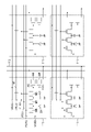
図2は、第1実施形態に係る画素111の回路構成を示す図である。図2には例示として、2行2列分の4つの画素111が示されている。画素111は、光電変換部D1、電荷保持部C1、第1転送トランジスタM1、第2転送トランジスタM2、リセットトランジスタM3、増幅トランジスタM4、選択トランジスタM5及び排出トランジスタM6を有する。これらのトランジスタは、例えばMOSトランジスタである。
FIG. 2 is a diagram showing the circuit configuration of the
光電変換部D1は、入射光を光電変換するとともに、光電変換によって生成される電荷を蓄積する。光電変換部D1としては、例えばフォトダイオードが用いられ得る。以下の説明では光電変換部D1はアノードとカソードを有するフォトダイオードであるものとする。光電変換部D1のアノードは接地電位線に接続されており、カソードは、第1転送トランジスタM1のソース及び排出トランジスタM6のソースに接続されている。第1転送トランジスタM1のドレインは第2転送トランジスタM2のソースに接続されている。第1転送トランジスタM1のドレインと第2転送トランジスタM2のソースとの間に寄生する容量は、電荷保持部C1を構成する。排出トランジスタM6のドレインは、排出電位VOFDを供給する電位線に接続されている。 The photoelectric conversion unit D1 photoelectrically converts incident light and accumulates charges generated by the photoelectric conversion. A photodiode, for example, can be used as the photoelectric conversion unit D1. In the following description, the photoelectric conversion unit D1 is assumed to be a photodiode having an anode and a cathode. The photoelectric conversion unit D1 has an anode connected to the ground potential line, and a cathode connected to the source of the first transfer transistor M1 and the source of the discharge transistor M6. The drain of the first transfer transistor M1 is connected to the source of the second transfer transistor M2. A parasitic capacitance between the drain of the first transfer transistor M1 and the source of the second transfer transistor M2 constitutes the charge holding portion C1. The drain of the drain transistor M6 is connected to a potential line that supplies the drain potential VOFD.
第2転送トランジスタM2のドレインは、リセットトランジスタM3のソース及び増幅トランジスタM4のゲートに接続されている。第2転送トランジスタM2のドレイン、リセットトランジスタM3のソース及び増幅トランジスタM4のゲートの接続ノードは、浮遊拡散領域FDである。リセットトランジスタM3のドレインは、リセット電位VRESを供給する電位線に接続されている。増幅トランジスタM4のソースは、選択トランジスタM5のドレインに接続されている。増幅トランジスタM4のドレインは、電源電圧線に接続されている。選択トランジスタM5のソースは、列信号線112に接続されている。列信号線112には不図示の電流源が接続されている。
The drain of the second transfer transistor M2 is connected to the source of the reset transistor M3 and the gate of the amplification transistor M4. A connection node of the drain of the second transfer transistor M2, the source of the reset transistor M3, and the gate of the amplification transistor M4 is the floating diffusion region FD. A drain of the reset transistor M3 is connected to a potential line that supplies a reset potential VRES. The source of the amplification transistor M4 is connected to the drain of the selection transistor M5. The drain of the amplification transistor M4 is connected to the power supply voltage line. A source of the selection transistor M5 is connected to the
画素アレイ110の各行には、行方向(図2において横方向)に延在して、複数の制御信号線が配されている。垂直走査回路120は、複数の制御信号線を介して画素111内のトランジスタに制御信号を供給する。垂直走査回路120は、制御信号PTX1、PTX2、PRES、PSEL、POFGを第1転送トランジスタM1、第2転送トランジスタM2、リセットトランジスタM3、選択トランジスタM5及び排出トランジスタM6のゲートにそれぞれ供給する。
Each row of the
第1転送トランジスタM1(電荷転送部)は、制御信号PTX1によりオンに制御されることにより、光電変換部D1で生成された電荷を電荷保持部C1に転送する。電荷保持部C1は、光電変換部D1から転送された電荷を保持する。第2転送トランジスタM2は、制御信号PTX2によりオンに制御されることにより、電荷保持部C1に保持された電荷を浮遊拡散領域FDに転送する。 The first transfer transistor M1 (charge transfer section) is turned on by the control signal PTX1 to transfer the charge generated in the photoelectric conversion section D1 to the charge holding section C1. The charge holding portion C1 holds the charge transferred from the photoelectric conversion portion D1. The second transfer transistor M2 is turned on by the control signal PTX2 to transfer the charge held in the charge holding portion C1 to the floating diffusion region FD.
リセットトランジスタM3は、制御信号PRESによりオンに制御されることにより、浮遊拡散領域FDの電位をリセットする。選択トランジスタM5は、制御信号PSELによりオンに制御されることにより、該当行の増幅トランジスタM4から列信号線112に信号を出力させる。このとき、増幅トランジスタM4と、列信号線112に接続された電流源は、浮遊拡散領域FDに転送された電荷に応じた信号を出力するソースフォロワ回路を構成することにより、出力部として機能する。排出トランジスタM6は、制御信号POFGによりオンに制御されることにより、光電変換部D1に蓄積されている電荷を排出し、光電変換部D1のカソードの電位をリセットする。
The reset transistor M3 resets the potential of the floating diffusion region FD by being turned on by the control signal PRES. The selection transistor M5 is turned on by the control signal PSEL to output a signal from the amplification transistor M4 of the corresponding row to the
これらの構成により、電荷保持部C1に電荷が保持されている間に光電変換部D1で電荷が生成され、光電変換部D1に蓄積される構成が実現される。これにより、撮像素子100は、画素アレイ110内の複数の光電変換部D1において電荷蓄積の開始時刻と終了時刻を一致させるグローバル電子シャッタ方式の駆動を行うことができる。グローバル電子シャッタ方式による電荷蓄積の開始は、例えば、画素アレイ110内の複数の排出トランジスタM6を同時にオンからオフに制御して電荷を排出することによって実現することができる。また、グローバル電子シャッタ方式による電荷蓄積の終了は、例えば、画素アレイ110内の複数の第1転送トランジスタM1を同時にオフからオンに制御し、再びオフに制御して電荷を転送することによって実現することができる。
With these configurations, a configuration is realized in which charges are generated in the photoelectric conversion unit D1 while charges are held in the charge holding unit C1 and accumulated in the photoelectric conversion unit D1. Thereby, the
なお、排出トランジスタM6は必須ではなく、光電変換部D1からの電荷の排出先を撮像素子100が形成されている半導体基板とするVertical Overflow Drainと呼ばれる構成に置き換えてもよい。また、電荷保持部C1の電位をリセットするための第2リセットトランジスタを更に追加してもよい。この場合、第2転送トランジスタM2をオンからオフにした後であって、光電変換部D1から電荷保持部C1に電荷を転送する前の期間に、当該第2リセットトランジスタをオンにして電荷保持部C1の電位をリセットしてもよい。
Note that the discharge transistor M6 is not essential, and may be replaced with a configuration called a vertical overflow drain in which the semiconductor substrate on which the
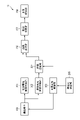
図3は、本実施形態の撮像装置10の概略構成を示すブロック図である。撮像装置10は、撮像素子100、短秒露光画像取得部201、長秒露光画像取得部202、多重露光制御部203、階調圧縮部204、環境光検出部205、画像合成部206、階調変換部207及び画像記録部208を備える。撮像素子100は、図1及び図2に示した構成のグローバル電子シャッタ方式のCMOSイメージセンサである。本実施形態では撮像素子100は、デジタルの画像データを出力するものとする。また、撮像素子100の出力ビット数は12ビットであり、すなわち、撮像素子100の出力値は、0から4095までの値を取り得る4096階調であるものとする。
FIG. 3 is a block diagram showing a schematic configuration of the
撮像素子100は、入射光による電荷の蓄積時間を相対的に短く設定した第1露光時間の第1画像データと、入射光による電荷の蓄積時間を相対的に長く設定した第2露光時間の第2画像データとを出力する。以下では、露光時間が相対的に短い第1露光時間を短秒露光、露光時間が相対的に長い第2露光時間を長秒露光と呼ぶこともある。
The
短秒露光画像取得部201(第1取得部)は、撮像素子100から出力される短秒露光の第1画像データを取得する。また、長秒露光画像取得部202(第2取得部)は、撮像素子100から出力される長秒露光の第2画像データを取得する。この、短秒露光の第1画像データと長秒露光の第2画像データは、たとえば1フレームごとに交互に撮像素子100の画像データ出力端子から出力される。
The short-second exposure image acquisition unit 201 (first acquisition unit) acquires the short-second exposure first image data output from the
環境光検出部205は、撮像装置10の撮像環境における環境光を検出して環境光情報を取得する部分である。環境光検出部205は、環境光の強度の変動を検出することにより、照明光源の点滅周期に関する情報を環境光情報として取得することができる。また、環境光検出部205は、昼夜、夕暮れなどの周囲の明るさ状況を検出することができる。環境光検出部205は、多重露光の回数と、低輝度部の階調値の減少割合(階調値圧縮割合)などを設定する多重露光制御部203の動作を決めるために、これらの環境光情報を取得する。環境光検出部205は、撮像装置10に搭載された環境光センサであり得る。なお、環境光検出部205は、他の装置から環境光情報を受信して、その環境光情報を多重露光制御部203に送信するものであってもよく、その場合、環境光検出部205は、環境光センサに代えてホストPC、マイクロコントローラ等であり得る。
The ambient
上述の第1画像データと第2画像データのうち、少なくとも第2画像データは、多重露光により取得された画像データである。多重露光とは、光電変換部D1から電荷保持部C1への電荷の転送を複数回に分けて行う処理である。なお、多重露光が行われる際の第1露光時間及び第2露光時間とは、複数回にわたって転送された電荷の露光時間の合計を意味するものとする。 Of the first image data and the second image data described above, at least the second image data is image data obtained by multiple exposure. Multiple exposure is a process in which charge is transferred from the photoelectric conversion portion D1 to the charge holding portion C1 in a plurality of times. It should be noted that the first exposure time and the second exposure time when multiple exposure is performed mean the total exposure time of charges transferred a plurality of times.
多重露光の処理は、多重露光制御部203により制御される。多重露光制御部203は、環境光検出部205からの環境光情報を受けて、周囲の環境光の状況に応じた多重露光制御信号を生成する。多重露光制御部203は、多重露光制御信号を撮像素子100及び階調圧縮部204に送信する。撮像素子100に送信される多重露光制御信号は、多重露光動作のオン/オフ、多重露光の回数、多重露光の間隔等の制御に用いられる。階調圧縮部204に送信される多重露光制御信号は、階調圧縮のオン/オフ、圧縮する階調数の範囲、圧縮時のビットシフト量等の制御に用いられる。
Multiple exposure processing is controlled by the multiple
階調圧縮部204(圧縮部)は、長秒露光画像取得部202により取得された長秒露光の第2画像データの階調値を減少させ、第3画像データを生成する。この処理は、具体的には、ビットシフトにより階調値を減少させてダイナミックレンジを圧縮するデジタル処理であり得る。これにより、低輝度のノイズが減少するようにダイナミックレンジを圧縮する画像処理が実現される。
The gradation compression unit 204 (compression unit) reduces the gradation value of the long-second exposure second image data acquired by the long-second exposure
画像合成部206は、短秒露光画像取得部201により取得された短秒露光の第1画像データと、階調圧縮部204から出力された第3画像データとを合成することにより、第4画像データを生成する。これにより、いわゆるハイダイナミックレンジ合成が行われ、ダイナミックレンジの広い第4画像データが生成される。
The
階調変換部207は、画像合成部206により生成された第4画像データを、ディスプレイ、画像記録部208等の出力系の機器の狭いダイナミックレンジに適した画像となるように階調変換を行う。これにより、出力系のダイナミックレンジに応じた適切な画像が生成される。この階調変換の処理は、例えば、ガンマ変換であり得る。階調変換部207で変換された画像データは、画像記録部208に出力される。画像記録部208は、例えば、ハードディスク、メモリカード等の記録装置である。なお、階調変換部207で変換された画像データは、画像記録部208に代えて液晶ディスプレイ等の表示装置に出力されてもよい。
The
以上のように、本実施形態では、短秒露光と長秒露光の2つの画像データからダイナミックレンジ合成画像を生成する。この合成処理では、画像中の明るい領域には短秒露光の画像データが用いられ、画像中の暗い領域には長秒露光の画像データが用いられる。これにより、明るい領域と暗い領域の両方を鮮明に表現することができるハイダイナミックレンジ合成が実現される。この技術は、例えば、明るい場所で逆光により影になっているときであっても人物の顔を認識する必要がある監視カメラ、トンネル内からトンネル外の明るい場所の信号機を認識する必要がある車載カメラ等に適用され得る。ここで、少なくとも長秒露光の第2画像データは、多重露光により取得された画像データである。まず、多重露光を行う理由について説明する。 As described above, in this embodiment, a dynamic range composite image is generated from two pieces of image data of short-second exposure and long-second exposure. In this synthesizing process, short-second exposure image data is used for bright areas in the image, and long-second exposure image data is used for dark areas in the image. This realizes high dynamic range synthesis that can clearly express both bright and dark areas. This technology is used, for example, in surveillance cameras that need to recognize people's faces even when they are in shadows due to backlight in bright places, and in-vehicle vehicles that need to recognize traffic lights in bright places outside tunnels. It can be applied to cameras and the like. Here, at least the second image data of long-second exposure is image data obtained by multiple exposure. First, the reason for performing multiple exposure will be described.
近年、照明用の光源が蛍光灯、白熱灯等からLEDに置き換えられている。LEDを用いた光源は、常時点灯ではなく、商用電源(50Hz又は60Hz)の倍以上の周波数で点滅するパルス点灯である場合がある。通常、この周波数は人が認識できる上限を超えているため、人の目にはこの点滅は認識されない。しかしながら、カメラにより60フレーム/秒等のフレーム周波数による動画撮影を行うと、光源の点滅と撮影のフレーム周波数との関係によっては、フレーム画像の明るさが周期的に変動するフリッカ現象が発生する場合がある。このフリッカ現象により、例えば、照明の明るさが周期的に変動しているように見える動画が撮影されることがある。また、信号機を撮影した場合には、常時点灯しているはずの信号機が点滅しているように撮影される場合もある。 In recent years, fluorescent lamps, incandescent lamps, and the like have been replaced with LEDs as light sources for illumination. A light source using an LED may not always be lit, but may be a pulsed light that blinks at a frequency more than twice that of a commercial power supply (50 Hz or 60 Hz). Normally, the human eye does not perceive this blinking because this frequency exceeds the upper limit of human perception. However, when moving images are captured with a camera at a frame frequency of 60 frames/second, etc., depending on the relationship between the flickering of the light source and the frame frequency of the shooting, a flicker phenomenon may occur in which the brightness of the frame image periodically fluctuates. There is Due to this flicker phenomenon, for example, a moving image may be captured in which the brightness of the illumination appears to fluctuate periodically. Moreover, when a traffic signal is photographed, the traffic signal which should always be lit may be photographed as if it were blinking.
本実施形態では、多重露光を行うことにより、このようなフリッカ現象による明るさの変動を低減することができる。多重露光は、光源の点滅の周波数よりも高い周波数で繰り返し露光を行うことにより、明るさを平均化する手法である。これにより、光源の点滅による明るさの変化の影響を低減することができる。次に、多重露光の具体的な処理について説明する。 In the present embodiment, by performing multiple exposure, it is possible to reduce the fluctuation in brightness due to such a flicker phenomenon. Multiple exposure is a method of averaging brightness by repeatedly exposing at a frequency higher than the frequency of blinking of the light source. As a result, it is possible to reduce the influence of changes in brightness due to blinking of the light source. Next, specific processing of multiple exposure will be described.
図4A及び図4Bは、第1実施形態に係る撮像装置10の動作を示すタイミング図である。図4A及び図4Bは、第1画像データと第2画像データのいずれか一方の画像を取得する際の処理を示している。図4Aは、複数フレームにわたる撮影処理の概略を示すタイミング図であり、図4Bは、1フレーム内の処理をより詳細に示すタイミング図である。
4A and 4B are timing charts showing the operation of the
図4Aには、電源波形PS、光源波形LS、及び制御信号POFG、PTX1、PTX2(i)、PTX2(i+1)、PTX2(i+2)、PTX2(k-1)、PTX2(k)のタイミングが示されている。図4Aの電源波形PSは、被写体を照らすLED照明等の光源に供給されている交流電源の波形を全波整流した形で模式的に示すものである。交流電源は、例えば、50Hzや60Hzの周波数で電力を供給する電源である。図4Aの期間T11は、交流電源の周期に相当しており、例えば、1/50秒又は1/60秒である。 FIG. 4A shows the timing of the power supply waveform PS, the light source waveform LS, and the control signals POFG, PTX1, PTX2(i), PTX2(i+1), PTX2(i+2), PTX2(k−1), PTX2(k). It is A power waveform PS in FIG. 4A schematically shows a waveform of AC power supplied to a light source such as an LED lighting for illuminating an object, in a full-wave rectified form. The AC power supply is, for example, a power supply that supplies power at a frequency of 50 Hz or 60 Hz. A period T11 in FIG. 4A corresponds to the cycle of the AC power supply, which is, for example, 1/50 second or 1/60 second.
図4Aの光源波形LSは、電源波形PSの電源を用いた光源の点灯状態を示すものである。光源波形LSにおいて、ハイレベルは点灯状態、ローレベルは消灯状態を示している。電源波形PSがある閾値以上の場合、光源波形LSはハイレベルであり、光源は点灯状態になっている。一方、電源波形PSが閾値未満の場合、光源波形LSはローレベルであり、光源は消灯状態になっている。上述のとおり、環境光検出部205は、環境光の強度の変動と、照明光源の点滅周期に関する情報を取得する。そのため、光源波形LSの波形自体、又は光源波形LSに基づく点滅周期等を取得することが可能である。
The light source waveform LS in FIG. 4A indicates the lighting state of the light source using the power source of the power source waveform PS. In the light source waveform LS, a high level indicates a lighting state, and a low level indicates a non-lighting state. When the power waveform PS is greater than or equal to a certain threshold, the light source waveform LS is at high level and the light source is on. On the other hand, when the power supply waveform PS is less than the threshold, the light source waveform LS is at low level and the light source is in the off state. As described above, the ambient
期間T12は、光源の点滅周期を示しており、交流電源の周期である期間T11の1/2の長さの周期である。また、期間T13は光源が点灯している期間を、期間T14は光源が消灯している期間をそれぞれ示している。 A period T12 indicates the flickering period of the light source, and is a period half the length of the period T11, which is the period of the AC power supply. A period T13 indicates a period in which the light source is turned on, and a period T14 indicates a period in which the light source is turned off.
図4Aの制御信号POFGは、排出トランジスタM6のゲートに供給されるパルス信号の波形を示している。制御信号POFGがローレベルからハイレベルになると、排出トランジスタM6がオンになり、光電変換部D1に蓄積されている電荷が排出電位VOFDを供給する電位線に排出される。本実施形態では、グローバル電子シャッタ方式による駆動が行われるため、すべての画素111において同じタイミングで制御信号POFGがハイレベルからローレベルになる。これにより、すべての画素111において同じタイミングで排出トランジスタM6がオンからオフになり、全ての画素111において同じタイミングで光電変換部D1での電荷蓄積が開始される。なお、本明細書において、「同じタイミング」とは、厳密に同時である必要はなく、グローバル電子シャッタ方式の駆動によって画像の歪みを抑制可能な程度に実質的に同じ時刻であればよい。
The control signal POFG in FIG. 4A shows the waveform of the pulse signal supplied to the gate of the discharge transistor M6. When the control signal POFG changes from low level to high level, the discharge transistor M6 is turned on, and the charges accumulated in the photoelectric conversion section D1 are discharged to the potential line supplying the discharge potential VOFD. In this embodiment, since driving is performed by the global electronic shutter method, the control signal POFG changes from high level to low level at the same timing in all the
図4Aの制御信号PTX1は、第1転送トランジスタM1のゲートに供給されるパルス信号の波形を示している。制御信号PTX1がローレベルからハイレベルになると、第1転送トランジスタM1がオンになり、光電変換部D1に蓄積されている電荷が電荷保持部C1に転送される。本実施形態では、グローバル電子シャッタ方式による駆動が行われるため、すべての画素111において同じタイミングで制御信号PTX1がハイレベルからローレベルになる。これにより、すべての画素111において同じタイミングで第1転送トランジスタM1がオフになり、全ての画素111において同じタイミングで光電変換部D1での電荷蓄積が終了される。
The control signal PTX1 in FIG. 4A indicates the waveform of the pulse signal supplied to the gate of the first transfer transistor M1. When the control signal PTX1 changes from low level to high level, the first transfer transistor M1 is turned on, and the charges accumulated in the photoelectric conversion portion D1 are transferred to the charge holding portion C1. In the present embodiment, since driving is performed by the global electronic shutter method, the control signal PTX1 changes from high level to low level at the same timing in all the
期間T15は、1回の電荷蓄積の開始から終了までの期間(サンプリング期間)を示している。本実施形態では、1フレーム期間内に短時間のサンプリング動作が複数回行われている。すなわち、すべての画素111において第1転送トランジスタM1が同じタイミングで間欠的に複数回オンになることによって、電荷が光電変換部D1から電荷保持部C1に間欠的に複数回転送されている。また、第1転送トランジスタM1がオンになる時刻においては、すべての画素111において排出トランジスタM6がオフとなるように、排出トランジスタM6も間欠的にオンとオフの動作が繰り返されている。このように、各サンプリング期間の開始と終了のタイミングを各行で一致させることにより、各行の露光時間を同一にすることができる。
A period T15 indicates a period (sampling period) from the start to the end of one charge accumulation. In this embodiment, short-time sampling operations are performed multiple times within one frame period. That is, in all the
図4Aの制御信号PTX2(i)、PTX2(i+1)、…は、第2転送トランジスタM2のゲートに供給されるパルス信号の波形を示している。括弧内の値は各制御信号が供給される画素アレイ110の行番号を示している。制御信号PTX2(i)がローレベルからハイレベルになると、i行目の第2転送トランジスタM2がオンになり、電荷保持部C1に保持された電荷が浮遊拡散領域FDに転送される。図4Aに示されるように、制御信号PTX2(i)、PTX2(i+1)、…は、行ごとに順次ハイレベルになる。これにより、第2転送トランジスタM2も行ごとに順次オンになり、電荷保持部C1に保持された電荷が浮遊拡散領域FDに転送される。
Control signals PTX2(i), PTX2(i+1), . The values in parentheses indicate the row numbers of the
ここで、期間T16は、複数回の電荷の転送の開始から終了までの期間であり、言い換えると、i行目の電荷保持部C1において電荷が保持されている期間である。期間T16において、第1転送トランジスタM1が間欠的に複数回オンになることによって、光電変換部D1から電荷保持部C1に複数回にわたって電荷が転送される。そのため、期間T16は、電荷保持部C1に保持される電荷が光電変換部D1で生成される期間であるともいえる。また、期間T16は、複数回行われるサンプリング動作において、最初のサンプリング動作の開始から、最後のサンプリング動作の終了までの期間に相当するともいえる。本実施形態では、上述のような複数回の転送により、電荷保持部C1には多重露光による信号電荷が蓄積される。同様に、期間T17は、i+1行目における最初のサンプリング動作の開始から、最後のサンプリング動作の終了までの期間を示している。 Here, the period T16 is a period from the start to the end of the charge transfer a plurality of times, in other words, a period during which the charge is held in the charge holding portion C1 of the i-th row. In the period T16, the first transfer transistor M1 is intermittently turned on multiple times, whereby charges are transferred from the photoelectric conversion unit D1 to the charge holding unit C1 multiple times. Therefore, it can be said that the period T16 is a period in which the charge held in the charge holding portion C1 is generated in the photoelectric conversion portion D1. It can also be said that the period T16 corresponds to the period from the start of the first sampling operation to the end of the last sampling operation in the sampling operations performed multiple times. In the present embodiment, signal charges due to multiple exposure are accumulated in the charge holding portion C1 by the multiple transfers as described above. Similarly, a period T17 indicates a period from the start of the first sampling operation on the (i+1)th row to the end of the last sampling operation.
期間T18(n)、T18(n+1)、…は、1フレームの期間を示している。括弧内の値はフレーム番号を示している。期間T18(n)、T18(n+1)、…のそれぞれにおいて、1フレーム分の画像データが撮像素子100から出力される。
Periods T18(n), T18(n+1), . . . indicate periods of one frame. Values in parentheses indicate frame numbers. In each of the periods T18(n), T18(n+1), . . . , one frame of image data is output from the
図4Bを参照して各制御信号の関係をより詳細に説明する。図4Bの制御信号PRES(i)、PRES(i+1)、…は、リセットトランジスタM3のゲートに供給されるパルス信号の波形を示している。括弧内の値は各制御信号が供給される画素アレイ110の行番号を示している。制御信号PRES(i)がローレベルからハイレベルになると、i行目のリセットトランジスタM3がオンになり、浮遊拡散領域FDの電位がリセットされる。図4Bに示されるように、制御信号PRES(i)、PRES(i+1)、…は、行ごとに順次ハイレベルになる。これにより、リセットトランジスタM3も行ごとに順次オンになり、浮遊拡散領域FDの電位がリセットされる。このリセットは、各行における電荷保持部C1から浮遊拡散領域FDへの電荷の転送の直前に行われる。なお、リセットトランジスタM3によるリセットの後及び第2転送トランジスタM2による転送の後には、列増幅回路140による信号の読み出しが行われる。リセット後に読み出された信号は、相関二重サンプリングによるノイズ低減に用いられる。
The relationship of each control signal will be described in more detail with reference to FIG. 4B. Control signals PRES(i), PRES(i+1), . . . in FIG. 4B show waveforms of pulse signals supplied to the gate of the reset transistor M3. The values in parentheses indicate the row numbers of the
期間T15は、図4Aと同様に1回のサンプリング期間を示している。期間T21は、i行目の読み出しが行われ、再度i行目の読み出しが行われる期間であり、その長さは、1フレームの期間と同様である。期間T22は、各行の信号が順次読み出される周期である、垂直走査周期を示すものである。本実施形態では、期間T21内に複数回のサンプリングが行われることにより、多重露光が実現される。以上のように、本実施形態では複数回のサンプリングを行い、電荷保持部C1内で平均化してから読み出すことにより、多重露光が実現される。これにより、光源の点灯時と消灯時の信号電荷が平均化されるため、フリッカ現象による画質への影響が低減される。 A period T15 indicates one sampling period as in FIG. 4A. A period T21 is a period in which the i-th row is read out and then the i-th row is read out again, and its length is the same as the period of one frame. A period T22 indicates a vertical scanning cycle, which is a cycle in which the signals of each row are read out sequentially. In the present embodiment, multiple exposure is realized by performing sampling a plurality of times within the period T21. As described above, in the present embodiment, multiple exposure is realized by sampling a plurality of times, averaging them in the charge holding unit C1, and then reading them out. As a result, signal charges when the light source is turned on and when the light source is turned off are averaged, so that the influence of the flicker phenomenon on image quality is reduced.
なお、期間T15の長さは、例えば、期間T12の長さの1/2以下としてもよい。この場合、複数回のサンプリングのうちのいずれかが消灯時に行われた場合でも、同じフレームの別のサンプリングが点灯時に行われる可能性が高くなり、多重露光によるフリッカ現象の影響の低減効果が向上する。また、期間T15の長さは、例えば、期間T15の長さは、期間T12の長さの1/4以下、1/8以下等のように期間T12の長さの1/2よりも更に小さく設定してもよい。この場合、フリッカ現象の影響の低減効果が更に向上する。 Note that the length of the period T15 may be, for example, half or less of the length of the period T12. In this case, even if one of the multiple samplings is performed when the lights are off, there is a high possibility that another sampling of the same frame will be performed when the lights are on, improving the effect of reducing the effects of flickering due to multiple exposures. do. In addition, the length of the period T15 is smaller than 1/2 of the length of the period T12, such as 1/4 or less, 1/8 or less of the length of the period T12, for example. May be set. In this case, the effect of reducing the influence of the flicker phenomenon is further improved.
期間T16は、期間T12よりも長く設定されていればよいが、期間T16の長さを期間T12に比べて2倍以上、3倍以上等のように大幅に長くしてもよい。この場合、光源の点灯時と消灯時の信号電荷との平均化の効果が大きくなり、フリッカ現象の影響の低減効果が更に向上する。また、例えば、期間T16の長さを、光源が点滅する周期の整数倍としてもよい。特に、商用電源のように周波数又は周期が既知である場合には、期間T16の長さを光源が点滅する周期の自然数倍(1以上の整数倍)とすることが容易である。この場合、期間T16内における光源の点滅回数が一定になるため、フリッカ現象の影響の低減効果が更に向上する。 The period T16 may be set longer than the period T12, but the length of the period T16 may be significantly longer than the period T12, such as twice or more, or three times or more. In this case, the effect of averaging the signal charges when the light source is turned on and when the light source is turned off increases, and the effect of reducing the influence of the flicker phenomenon is further improved. Also, for example, the length of the period T16 may be an integral multiple of the blinking cycle of the light source. In particular, when the frequency or cycle is known, such as with a commercial power supply, it is easy to set the length of the period T16 to a natural number multiple (an integer multiple of 1 or more) of the blinking cycle of the light source. In this case, since the number of times the light source blinks during the period T16 is constant, the effect of reducing the influence of the flicker phenomenon is further improved.
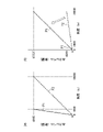
図5(a)及び図5(b)は、第1実施形態に係るダイナミックレンジ拡大処理における照度と出力レベルの関係の例を示すグラフである。図5(a)及び図5(b)を参照して、画像合成部206により行われるハイダイナミックレンジ合成処理の概略を説明する。
FIGS. 5A and 5B are graphs showing examples of the relationship between illuminance and output level in dynamic range expansion processing according to the first embodiment. The outline of the high dynamic range combining processing performed by the
ハイダイナミックレンジ合成処理の一例として、露光時間の短い画像データと露光時間の長い画像データとを合成する処理を説明する。ここでは、2つの画像データの階調数は4096階調(12ビット)であるものとし、合成後の画像データの階調数は65536階調(16ビット)相当であるものとする。この場合、ダイナミックレンジは、72dB相当から96dB相当に拡大する。 As an example of high dynamic range synthesis processing, processing for synthesizing image data with a short exposure time and image data with a long exposure time will be described. Here, the number of gradations of the two image data is assumed to be 4096 gradations (12 bits), and the number of gradations of the combined image data is equivalent to 65536 gradations (16 bits). In this case, the dynamic range is expanded from equivalent to 72 dB to equivalent to 96 dB.
図5(a)は、画像合成前における照度と出力レベル(階調)との関係を示すグラフである。特性P1は、主に被写体の暗部領域の撮像に用いられるものであり、露光時間の長い画像の撮像時の照度に対する出力レベル特性である。特性P2は、主に被写体の明部領域の撮像に用いられるものであり、露光時間の短い画像の撮像時の照度に対する出力レベル特性である。特性P2の傾きは、特性P1の傾きと比較して緩やかである。ここでは、特性P1における露光時間は、特性P2における露光時間の16倍であるものとする。より具体的には、露光時間の長い画像の撮像時の出力レベルは、照度が1000ルクス(lx)で4095階調に達するのに対して、露光時間の短い画像の撮像時の出力レベルは、照度が16倍の16000lxで4095階調に達するように設定されている。 FIG. 5A is a graph showing the relationship between illuminance and output level (gradation) before image synthesis. The characteristic P1 is mainly used for imaging a dark area of a subject, and is an output level characteristic with respect to illuminance when an image with a long exposure time is captured. The characteristic P2 is mainly used for imaging a bright area of a subject, and is an output level characteristic with respect to illuminance when an image with a short exposure time is captured. The slope of the characteristic P2 is gentler than the slope of the characteristic P1. Here, it is assumed that the exposure time for the characteristic P1 is 16 times the exposure time for the characteristic P2. More specifically, the output level when capturing an image with a long exposure time reaches 4095 gradations at an illuminance of 1000 lux (lx), while the output level when capturing an image with a short exposure time is The illuminance is set to reach 4095 gradations at 16000 lx, which is 16 times.
まず、露光時間の短い画像データをデジタル的に4ビットだけ上位側にビットシフトした画像を作成する。これによって、短い時間に露光で撮像された画像データは、階調数65536階調の16ビットのデータとなる。次に、シフト後の露光時間の短い画像データと露光時間の長い画像データとの合成を行う。この合成処理は、ある閾値以下の階調値では露光時間の長い画像データを用い、ある閾値よりも大きい階調値ではシフト後の露光時間の短い画像データを用いるというものであり得る。これにより、ダイナミックレンジが拡大された16ビットの画像データが生成される。本例では、閾値が4095階調であるものとする。 First, an image is created by digitally shifting image data with a short exposure time by 4 bits to the upper side. As a result, the image data captured by exposure in a short period of time becomes 16-bit data with 65536 gradations. Next, image data with a short exposure time after the shift and image data with a long exposure time are combined. This synthesizing process can be such that image data with a long exposure time is used for tone values equal to or less than a certain threshold, and image data with a short exposure time after shift is used for tone values greater than a certain threshold. As a result, 16-bit image data with an expanded dynamic range is generated. In this example, it is assumed that the threshold is 4095 gradations.
図5(b)は、画像合成後における照度と出力レベル(階調)との関係を示すグラフである。特性P1は、閾値である4095階調以下であるため、露光時間の長い画像に係る特性と同一である。特性P3は、閾値である4095階調よりも大きいことから、シフト後の露光時間の短い画像データの特性と同一である。特性P3は、特性P2を4ビットだけ上位側にシフトしたものである。合成後の画像の特性は、特性P1と特性P3をつなげたものに相当する。これによって合成後の画像は、16ビットの階調精度を有しながら、飽和レベルが16倍に大きくなっており、ダイナミックレンジの拡大された画像となる。本例においては、露光時間の比率は16倍としているが、更に露光時間の比を大きく設定することで、100dB以上の高いダイナミックレンジを有する画像を得ることも可能である。 FIG. 5B is a graph showing the relationship between illuminance and output level (gradation) after image synthesis. Since the characteristic P1 is equal to or less than the threshold value of 4095 gradations, it is the same as the characteristic related to an image with a long exposure time. Since the characteristic P3 is larger than the threshold value of 4095 gradations, it is the same as the characteristic of image data with a short exposure time after the shift. The characteristic P3 is obtained by shifting the characteristic P2 by 4 bits to the upper side. The characteristics of the combined image correspond to the combination of characteristics P1 and P3. As a result, the synthesized image has a 16-bit gradation accuracy and a 16-fold increase in saturation level, resulting in an image with an expanded dynamic range. In this example, the exposure time ratio is set to 16 times, but it is possible to obtain an image with a high dynamic range of 100 dB or more by setting the exposure time ratio to a larger value.
本実施形態によれば、上述の多重露光と画像合成によるダイナミックレンジ拡大を組み合わせることによって、フリッカ現象による画質への影響低減とダイナミックレンジ拡大とを両立した高品質な撮像を実現することができる。 According to this embodiment, by combining the above-described multiple exposure and dynamic range expansion by image synthesis, it is possible to achieve high-quality imaging that achieves both reduction in the effect of flicker on image quality and expansion of the dynamic range.
しかしながら、多重露光においては複数回にわたって転送された電荷が電荷保持部C1において加算されるため、画素欠陥、固定パターンノイズ、面内ムラ等に起因するノイズが多重露光の回数分だけ重畳されて画質が劣化する場合がある。特に、上述のダイナミックレンジ拡大後の画像においては、画像中の暗部に相当する部分の撮像に多重露光が用いられると、画質劣化が顕著になる。そこで、本実施形態では、階調圧縮部204は、多重露光された画像に対してダイナミックレンジ拡大の画像合成を行う前に、階調圧縮の処理を行う。階調圧縮部204は、多重露光により得られた長秒露光の第2画像データを階調圧縮する。これにより、画素欠陥等に起因するノイズのレベルが低減される。
However, in multiple exposure, the charges transferred a plurality of times are added in the charge holding portion C1, so noise caused by pixel defects, fixed pattern noise, in-plane unevenness, etc. is superimposed for the number of times of multiple exposure, resulting in poor image quality. may deteriorate. In particular, in the image after the dynamic range expansion described above, if multiple exposure is used to capture a portion corresponding to a dark portion in the image, image quality deterioration becomes noticeable. Therefore, in the present embodiment, the
図6(a)乃至図6(c)は、第1比較例に係るダイナミックレンジ拡大処理を説明する模式図である。図7(a)乃至図7(c)は、第2比較例に係るダイナミックレンジ拡大処理を説明する模式図である。図8(a)乃至図8(c)は、第1実施形態に係るダイナミックレンジ拡大処理を説明する模式図である。これらの図を参照しつつ、ダイナミックレンジ拡大、多重露光及び階調圧縮の効果を説明する。 FIGS. 6A to 6C are schematic diagrams for explaining dynamic range expansion processing according to the first comparative example. FIGS. 7A to 7C are schematic diagrams for explaining dynamic range expansion processing according to the second comparative example. FIGS. 8A to 8C are schematic diagrams for explaining dynamic range expansion processing according to the first embodiment. The effects of dynamic range expansion, multiple exposure, and gradation compression will be described with reference to these figures.
まず、第1比較例を説明する。図6(a)乃至図6(c)に示す第1比較例は、多重露光制御部203による多重露光の制御を行わず、かつ階調圧縮部204での階調圧縮も行わない場合の例である。図6(a)乃至図6(c)は、第1比較例でのダイナミックレンジ拡大処理時の信号レベルの変化を示す模式図である。
First, a first comparative example will be described. A first comparative example shown in FIGS. 6A to 6C is an example in which the multiple
図6(a)は、長秒露光画像取得部202により取得される長秒露光の第2画像データの信号レベルの模式図である。図5(a)及び図5(b)の例と同様に、撮像素子100は12ビット(4096階調)のデジタル信号を出力するものとする。このとき、第2画像データには、図6(a)に示されるように信号成分S11に、2ビット相当のノイズ成分N11が含まれているものとする。
FIG. 6A is a schematic diagram of the signal level of the second long-second exposure image data acquired by the long-second exposure
図6(b)は、短秒露光画像取得部201により取得される短秒露光の第1画像データの信号レベルの模式図である。撮像素子100は、長秒露光の場合と同様に12ビット(4096階調)のデジタル信号を出力する。このとき、第1画像データには、図6(b)に示されるように信号成分S12に、1ビット相当のノイズ成分N12が含まれているものとする。画像合成部206は、第1画像データを4ビットだけ上位側にビットシフトする。信号成分S13は、ビットシフト後の信号成分を示しており、ノイズ成分N13は、ビットシフト後のノイズ成分を示している。4ビット分のビットシフトにより、ノイズ成分N13の大きさは、1ビット相当から5ビット相当に大きくなっている。
FIG. 6B is a schematic diagram of the signal level of the first image data of the short-second exposure acquired by the short-second exposure
図6(c)は、画像合成部206における合成の前後での信号レベルの模式図である。第1比較例では、階調圧縮部204での階調圧縮は行われないため、長秒露光の第2画像データは、そのまま、4ビット分だけビットシフトされた短秒露光の第1画像データと合成される。合成後の出力信号のうちの4095階調以上の範囲である信号成分S14には短秒露光の第1画像データが用いられる。また、合成後の出力信号のうちの4095階調未満の範囲である信号成分S15には長秒露光の第2画像データが用いられる。合成後の出力信号に含まれるノイズ成分N14は、長秒露光の第2画像データに含まれるノイズ成分N11と同一である。したがって、ノイズ成分N14のレベルは2ビット相当である。この例では多重露光を行わないため、多重露光によるノイズの増加はない。しかしながら、第1比較例の構成では上述のようにフリッカ現象による画質の劣化が生じる場合がある。
FIG. 6C is a schematic diagram of signal levels before and after combining in the
次に、第2比較例を説明する。図7(a)乃至図7(c)に示す第2比較例は、多重露光制御部203による多重露光の制御を行うが、階調圧縮部204での階調圧縮は行わない場合の例である。図7(a)乃至図7(c)は、第2比較例でのダイナミックレンジ拡大処理時の信号レベルの変化を示す模式図である。
Next, a second comparative example will be described. A second comparative example shown in FIGS. 7A to 7C is an example in which the multiple
図7(a)は、長秒露光画像取得部202により取得される長秒露光の第2画像データの信号レベルの模式図である。図5(a)及び図5(b)の例と同様に、撮像素子100は12ビット(4096階調)のデジタル信号を出力するものとする。このとき、図7(a)左側に示されるように、1回の露光に対して2ビット相当のノイズ成分N11が含まれる信号成分S11が生じるものとする。
FIG. 7A is a schematic diagram of the signal level of the second long-second exposure image data acquired by the long-second exposure
本例では、多重露光の回数が4回であるものとすると、4回の露光により図7(a)右側のように信号成分S21、S22、S23、S24が生じ、これらが加算された信号が第2画像データとして出力される。このとき、撮像素子100の出力範囲は12ビット(4096階調)であるため、4095以上の出力レベルはすべて上限値4095でクリップされる。このときに生じるノイズ成分N21の大きさは、1回の露光に対するノイズ成分N11の大きさの4倍になるため、4ビット相当に大きくなっている。
In this example, assuming that the number of multiple exposures is four, the four exposures generate signal components S21, S22, S23, and S24 as shown on the right side of FIG. It is output as the second image data. At this time, since the output range of the
図7(b)は、短秒露光画像取得部201により取得される短秒露光の第1画像データの信号レベルの模式図である。これは第1比較例と同様であるため説明を省略する。
FIG. 7B is a schematic diagram of the signal level of the first image data of the short-second exposure acquired by the short-second exposure
図7(c)は、画像合成部206における合成の前後での信号レベルの模式図である。第2比較例においても、階調圧縮部204での階調圧縮は行われないため、長秒露光の第2画像データは、そのまま4ビット分ビットシフトされた短秒露光の第1画像データと合成される。この場合も第1比較例と同様に、合成後の出力信号に含まれるノイズ成分N22は、長秒露光の第2画像データに含まれるノイズ成分N21と同一である。したがって、ノイズ成分N22のレベルは4ビット相当である。この例では、多重露光を行ったことによりフリッカ現象の影響は低減されるものの、ノイズ成分N22のレベルが増加する点が問題となり得る。
FIG. 7C is a schematic diagram of signal levels before and after combining in the
次に、本実施形態の構成におけるノイズ成分の変化を説明する。図8(a)乃至図8(c)に示す例は、本実施形態に相当する例であり、多重露光制御部203による多重露光の制御を行い、かつ階調圧縮部204での階調圧縮も行う場合を示している。図8(a)乃至図8(c)は、本実施形態でのダイナミックレンジ拡大処理時の信号レベルの変化を示す模式図である。
Next, changes in noise components in the configuration of this embodiment will be described. The examples shown in FIGS. 8A to 8C are examples corresponding to this embodiment, in which multiple exposure is controlled by the multiple
図8(a)は、長秒露光画像取得部202により取得される長秒露光の第2画像データの信号レベルの模式図及び階調圧縮部204による圧縮後の第3画像データの信号レベルの模式図である。図8(a)の左側及び中央に示される第2画像データの信号レベルは図7(a)と同様である。図8(a)の右側は、階調圧縮部204による圧縮後の第3画像データの信号レベルを示している。この処理では12ビットのデータを10ビットに圧縮する処理が行われている。この圧縮処理は具体的には、データを2ビットだけ下位側にビットシフトするものであってもよく、データを係数4で除算するものであってもよい。この処理により、第3画像データの信号成分S31の階調値は1/4に小さくなっており、階調数は1024階調に減少している。このとき、ノイズ成分N31の大きさも4ビット相当から2ビット相当に低減されている。したがって、階調圧縮部204により階調圧縮の処理を行って階調数を減少させることにより、多重露光により増大したノイズが低減される。
FIG. 8A is a schematic diagram of the signal level of the second long-second exposure image data acquired by the long-second exposure
図8(b)は、短秒露光画像取得部201により取得される短秒露光の第1画像データの信号レベルの模式図である。これは第1比較例及び第2比較例と同様であるため説明を省略する。
FIG. 8B is a schematic diagram of the signal level of the first image data of the short-second exposure acquired by the short-second exposure
図8(c)は、画像合成部206における合成の前後での信号レベルの模式図である。本実施形態では、階調圧縮部204での階調圧縮により生成された第3画像データと、4ビット分ビットシフトされた短秒露光の第1画像データとが合成される。合成後の出力信号に含まれるノイズ成分N32は、階調圧縮後の第3画像データに含まれるノイズ成分N31と同一である。したがって、ノイズ成分N32のレベルは2ビット相当であり、当初のノイズ成分N11と同等である。本実施形態では、多重露光を行ったことによりフリッカ現象の影響は低減される。さらに、多重露光によるノイズの増大の影響も階調圧縮により緩和される。
FIG. 8C is a schematic diagram of signal levels before and after combining in the
図9は、第1実施形態に係る撮像装置10の動作を示すフローチャートである。図9を参照して撮像装置10の動作を説明する。上述の説明において説明済みの処理についてはは説明を省略又は簡略化することがある。
FIG. 9 is a flow chart showing the operation of the
ステップS101において、多重露光制御部203は、環境光検出部205により取得された環境光情報に基づいて、多重露光制御信号を撮像素子100に送信して短秒露光のための第1露光時間を設定する。
In step S101, the multiple
ステップS102において、撮像素子100は、短秒露光による撮像を行い、第1画像データを出力する。そして、短秒露光画像取得部201は、撮像素子100から短秒露光の第1画像データを取得する。
In step S102, the
ステップS103において、多重露光制御部203は、環境光検出部205により取得された環境光情報に基づいて、多重露光制御信号を撮像素子100に送信して長秒露光のための第2露光時間を設定する。
In step S103, the multiple
ステップS104において、撮像素子100は、長秒露光による撮像を行い、第2画像データを出力する。そして、長秒露光画像取得部202は、撮像素子100から長秒露光の第2画像データを取得する。ステップS105において、階調圧縮部204は、第2画像データの階調数を減少させる階調圧縮を行い、第3画像データを生成し、取得する。このとき、階調圧縮部204は、環境光検出部205により取得された環境光情報に基づいて、多重露光制御部203が定めた制御信号により、取得した長秒露光画像の圧縮割合を制御する。
In step S104, the
ステップS106において、画像合成部206は、第1画像データと、第3画像データとを合成する。これにより、いわゆるハイダイナミックレンジ合成が行われ、ダイナミックレンジの広い第4画像データが生成される。ステップS107において、階調変換部207は、画像記録部208等の出力系の機器の狭いダイナミックレンジに適した画像となるように、第4画像データの階調変換を行う。ステップS108において、画像記録部208は、階調変換後の画像データを記録する。なお、動画の撮影時においては、ステップS101からステップS108の処理が連続的に繰り返され、動画ファイルが生成される。
In step S106, the
本実施形態では、撮像素子100は、短秒露光の第1画像データと、長秒露光の第2画像データを出力する。ここで、少なくとも長秒露光は、光電変換部D1から電荷保持部C1に複数回にわたって電荷が転送される多重露光である。階調圧縮部204は第2画像データの階調値を減少させて第3画像データを生成する。このようにして、本実施形態の撮像装置10は、画質を維持しつつフリッカ現象の影響を低減することが可能で、かつ露光時間の異なる複数の画像(第1画像データ及び第3画像データ)を取得することができる。また、撮像装置10で取得された第1画像データ及び第3画像データはハイダイナミックレンジ合成に用いられるため、本実施形態によれば、高画質なハイダイナミックレンジ画像を生成することができる。
In this embodiment, the
なお、本実施形態においては、少なくとも第2画像データが多重露光により生成されればよいが、第1画像データと第2画像データの両方が多重露光により生成されることが望ましい。この場合、画像中の階調値の小さい箇所と階調値が大きい箇所のいずれにおいてもフリッカ減少の影響を抑制することができる。 In this embodiment, at least the second image data should be generated by multiple exposure, but it is desirable that both the first image data and the second image data are generated by multiple exposure. In this case, it is possible to suppress the influence of flicker reduction in both locations with small gradation values and locations with large gradation values in the image.
また、図3において、撮像素子100以外の要素(画像合成部206等)は、撮像素子100の外部に設けられているように図示されているが、これらの要素の一部又は全部は、撮像素子100の内部に設けられていてもよい。また、画像合成部206、階調変換部207及び画像記録部208の一部又は全部は、撮像装置10の外部の画像処理装置に設けられていてもよい。
Further, in FIG. 3, elements other than the image sensor 100 (such as the image synthesizing unit 206) are illustrated as being provided outside the
[第2実施形態]
本発明の第2実施形態を説明する。本実施形態が第1実施形態と異なる点は、短秒露光の第1画像データの取得と長秒露光の第2画像データの取得が同一フレームに行われ得る点である。第1実施形態においては、撮像素子100は、短秒露光の第1画像データと長秒露光の第2画像データを同一フレーム期間内に出力することを想定していない回路構成となっている。そのため、第1実施形態では、あるフレームで短秒露光の第1画像データを出力し、別のフレームで長秒露光の第2画像データを出力するというような方法によりフレームを分けて画像データの読み出しを行う必要がある。これに対し、本実施形態では、各画素に複数の電荷保持部を設けることにより、短秒露光の第1画像データの取得と長秒露光の第2画像データの取得を同一フレームに行うことができる。以下の説明において、第1実施形態と共通する部分については、適宜説明を省略する。
[Second embodiment]
A second embodiment of the present invention will be described. This embodiment differs from the first embodiment in that acquisition of first image data for short-second exposure and acquisition of second image data for long-second exposure can be performed in the same frame. In the first embodiment, the
図10は、第2実施形態に係る画素113の回路構成を示す図である。本実施形態では、各画素113内に第1転送トランジスタ、電荷保持部及び第2転送トランジスタが2個ずつ設けられている点が第1実施形態と異なる。すなわち、画素113には、第1実施形態の第1転送トランジスタM1、電荷保持部C1及び第2転送トランジスタM2に代えて、第1転送トランジスタM1A、M1B、電荷保持部C1A、C1B及び第2転送トランジスタM2A、M2Bが設けられている。
FIG. 10 is a diagram showing the circuit configuration of the
第1転送トランジスタM1A、M1Bのソースは、いずれも光電変換部D1のカソード及び排出トランジスタM6のソースに接続されている。第1転送トランジスタM1Aのドレインは第2転送トランジスタM2Aのソースに接続されている。第1転送トランジスタM1Aのドレインと第2転送トランジスタM2Aのソースとの間に寄生する容量は、電荷保持部C1Aを構成する。第1転送トランジスタM1Bのドレインは第2転送トランジスタM2Bのソースに接続されている。第1転送トランジスタM1Bのドレインと第2転送トランジスタM2Bのソースとの間に寄生する容量は、電荷保持部C1Bを構成する。第2転送トランジスタM2A、M2Bのドレインは、いずれもリセットトランジスタM3のソース及び増幅トランジスタM4のゲートに接続されている。垂直走査回路120は、制御信号PTX1A、PTX1Bを第1転送トランジスタM1A、M1Bのゲートにそれぞれ供給する。また、垂直走査回路120は、制御信号PTX2A、PTX2Bを第2転送トランジスタM2A、M2Bのゲートにそれぞれ供給する。
The sources of the first transfer transistors M1A and M1B are both connected to the cathode of the photoelectric conversion unit D1 and the source of the discharge transistor M6. The drain of the first transfer transistor M1A is connected to the source of the second transfer transistor M2A. A parasitic capacitance between the drain of the first transfer transistor M1A and the source of the second transfer transistor M2A constitutes the charge holding portion C1A. The drain of the first transfer transistor M1B is connected to the source of the second transfer transistor M2B. A parasitic capacitance between the drain of the first transfer transistor M1B and the source of the second transfer transistor M2B constitutes the charge holding portion C1B. The drains of the second transfer transistors M2A and M2B are both connected to the source of the reset transistor M3 and the gate of the amplification transistor M4. The
このような構成により、電荷保持部C1Aに電荷が保持されている状態であっても、電荷保持部C1Bに更に電荷を転送することができる。このため、電荷保持部C1A、C1Bに同一フレームの互いに異なる信号を保持することが可能となる。また、電荷保持部C1A、C1Bに対して第1転送トランジスタM1A、M1Bが独立して設けられているため、電荷保持部C1A、C1Bに露光時間の異なるサンプリング動作を同一フレーム期間内に順次行うことができる。言い換えると、本実施形態の撮像装置10は、第1画像データと第2画像データを同一のフレーム期間に取得することができる。
With such a configuration, even when charges are held in the charge holding portion C1A, charges can be further transferred to the charge holding portion C1B. Therefore, different signals of the same frame can be held in the charge holding units C1A and C1B. In addition, since the first transfer transistors M1A and M1B are provided independently for the charge holding units C1A and C1B, the charge holding units C1A and C1B can be sequentially subjected to sampling operations with different exposure times within the same frame period. can be done. In other words, the
図11は、第2実施形態に係る撮像装置10の動作を示すタイミング図である。図11には、電源波形PS及び制御信号POFG、PTX1A、PTX1B、PTX2A(i)、PTX2B(i)、PTX2A(i+1)、PTX2B(i+1)、PTX2A(i+2)、PTX2B(i+2)のタイミングが示されている。括弧内の値は、第1実施形態と同様に画素アレイ110の行番号を示している。電源波形PS及び電源波形PSに基づく電力が供給される光源については第1実施形態と同様であるため説明を省略する。
FIG. 11 is a timing chart showing operations of the
制御信号POFGがローレベルからハイレベルになると、排出トランジスタM6がオンになり、光電変換部D1に蓄積されている電荷が排出電位VOFDを供給する電位線に排出される。制御信号PTX1Aがローレベルからハイレベルになると、第1転送トランジスタM1Aがオンになり、光電変換部D1に蓄積されている電荷が電荷保持部C1Aに転送される。制御信号PTX1Bがローレベルからハイレベルになると、第1転送トランジスタM1Bがオンになり、光電変換部D1に蓄積されている電荷が電荷保持部C1Bに転送される。本実施形態においても、第1実施形態と同様にグローバル電子シャッタ方式による駆動が行われるため、すべての画素111において同じタイミングで制御信号POFG、PTX1A、PTX1Bのレベルが変動する。
When the control signal POFG changes from low level to high level, the discharge transistor M6 is turned on, and the charges accumulated in the photoelectric conversion section D1 are discharged to the potential line supplying the discharge potential VOFD. When the control signal PTX1A changes from low level to high level, the first transfer transistor M1A is turned on, and the charge accumulated in the photoelectric conversion section D1 is transferred to the charge holding section C1A. When the control signal PTX1B changes from low level to high level, the first transfer transistor M1B is turned on, and the charges accumulated in the photoelectric conversion portion D1 are transferred to the charge holding portion C1B. Also in this embodiment, driving by the global electronic shutter method is performed as in the first embodiment, so that the levels of the control signals POFG, PTX1A, and PTX1B fluctuate at the same timing in all the
期間T32A、T32Bは、1回の電荷蓄積の開始から終了までの期間(サンプリング期間)を示している。期間T32Aは、電荷保持部C1Aに転送され、保持される電荷についてのサンプリング期間であり、期間T32Bは電荷保持部C1Bに転送され、保持される電荷についてのサンプリング期間である。 Periods T32A and T32B indicate periods (sampling periods) from the start to the end of one charge accumulation. A period T32A is a sampling period for charges transferred to and held in the charge holding portion C1A, and a period T32B is a sampling period for charges transferred to and held in the charge holding portion C1B.
図11に示されるように、期間T32Bの長さは期間T32Aの長さよりも長い。そのため、電荷保持部C1A、C1Bには、蓄積時間の異なる電荷が蓄積される。すなわち、期間T32Aは短秒露光に対応するサンプリング期間であり、期間T32Bは長秒露光に相当するサンプリング期間である。これにより、同一フレーム期間内に露光時間の異なるサンプリング動作を行うことができる。 As shown in FIG. 11, the length of period T32B is longer than the length of period T32A. Therefore, charges with different accumulation times are accumulated in the charge holding units C1A and C1B. That is, the period T32A is a sampling period corresponding to short-second exposure, and the period T32B is a sampling period corresponding to long-second exposure. As a result, sampling operations with different exposure times can be performed within the same frame period.
図11では、期間T32Aと期間T32Bは交互に配されており、互いに重複していないが、期間T32Bと期間T32Aの長さが異なっていればこれらの一部が重複していてもよい。また、図11において、制御信号PTX1Aがハイレベルになる周期と制御信号PTX1Bがハイレベルになる周期とは同一であるが、これらは互いに異なっていてもよい。この場合、短秒露光と長秒露光とで多重露光の回数が異なる画像データが得られるがこれも許容される。 In FIG. 11, the periods T32A and T32B are alternately arranged and do not overlap each other, but if the lengths of the periods T32B and T32A are different, they may partially overlap. Also, in FIG. 11, the period in which the control signal PTX1A goes high and the period in which the control signal PTX1B goes high are the same, but they may be different. In this case, image data with different numbers of multiple exposures can be obtained by short-second exposure and long-second exposure, but this is also acceptable.
制御信号PTX2A(i)がハイレベルになると、i行目の第2転送トランジスタM2Aがオンになり、電荷保持部C1Aに保持された電荷が浮遊拡散領域FDに転送される。また、制御信号PTX2B(i)がハイレベルになると、i行目の第2転送トランジスタM2Bがオンになり、電荷保持部C1Bに保持された電荷が浮遊拡散領域FDに転送される。 When the control signal PTX2A(i) becomes high level, the i-th second transfer transistor M2A is turned on, and the charge held in the charge holding portion C1A is transferred to the floating diffusion region FD. Further, when the control signal PTX2B(i) becomes high level, the i-th second transfer transistor M2B is turned on, and the charge held in the charge holding portion C1B is transferred to the floating diffusion region FD.
期間T33Aは、i行目の電荷保持部C1Aにおいて電荷が保持されている期間であり、期間T33Bは、i行目の電荷保持部C1Bにおいて電荷が保持されている期間である。期間T33A、T33Bの間に第1転送トランジスタM1A、M1Bが間欠的に複数回オンになることにより、複数回のサンプリングが行われるので、第1実施形態と同様に多重露光が実現される。これにより、第1実施形態と同様にフリッカ現象の影響が低減される。本例では、期間T33A、T33Bのそれぞれにおいて3回のサンプリングが行われている。期間T36(n)、T36(n+1)、…は、1フレームの期間を示している。括弧内の値はフレーム番号を示している。期間T36(n)、T36(n+1)、…のそれぞれにおいて、1フレーム分の画像データが撮像素子100から出力される。
A period T33A is a period in which charges are held in the i-th charge holding portion C1A, and a period T33B is a period in which charges are held in the i-th charge holding portion C1B. By intermittently turning on the first transfer transistors M1A and M1B a plurality of times during the periods T33A and T33B, sampling is performed a plurality of times, so multiple exposure is realized as in the first embodiment. As a result, the influence of the flicker phenomenon is reduced as in the first embodiment. In this example, three samplings are performed in each of periods T33A and T33B. Periods T36(n), T36(n+1), . . . indicate periods of one frame. Values in parentheses indicate frame numbers. In each of the periods T36(n), T36(n+1), . . . , one frame of image data is output from the
本実施形態では、第1実施形態と同様に、短秒露光の第1画像データと、長秒露光の第2画像データを生成することができ、第1実施形態と同様に多重露光が実現可能な構成となっている。本実施形態の撮像装置10は、第1実施形態と同様に、画質を維持しつつフリッカ現象の影響を低減することが可能で、かつ露光時間の異なる複数の画像(第1画像データ及び第3画像データ)を取得することができる。更に、本実施形態では、短秒露光の第1画像データの取得と長秒露光の第2画像データの取得を同一フレームに行うことができる。これにより、ハイダイナミックレンジ合成に用いられる2つの画像の撮影時間を近づけることができ、合成後の画像の画質がより向上する効果が得られる。
In the present embodiment, as in the first embodiment, it is possible to generate first image data of short-second exposure and second image data of long-second exposure, and multiple exposure can be realized as in the first embodiment. configuration. As in the first embodiment, the
[第3実施形態]
次に、上述の実施形態による撮像装置を適用した装置の例を説明する。図12は、本実施形態による撮像システム500の構成を示すブロック図である。図12に示す撮像装置10は、上述の第1又は第2実施形態で述べた撮像装置10のいずれかである。撮像装置10が適用可能な撮像システム500としては、例えば、デジタルカメラ、デジタルカムコーダー、監視カメラなどが挙げられる。図5に、上述の実施形態に記載の撮像装置10を適用したデジタルカメラの構成例を示す。
[Third embodiment]
Next, an example of an apparatus to which the imaging apparatus according to the above-described embodiment is applied will be described. FIG. 12 is a block diagram showing the configuration of an
図12に例示した撮像システム500は、撮像装置10、被写体の光学像を撮像装置10に結像させるレンズ502、レンズ502を通過する光量を可変にするための絞り504、レンズ502の保護のためのバリア506を有する。レンズ502及び絞り504は、撮像装置10に光を集光する光学系である。
An
撮像システム500は、また、撮像装置10から出力される出力信号の処理を行う信号処理部508を有する。信号処理部508は、必要に応じて入力信号に対して各種の補正、圧縮を行って出力する信号処理の動作を行う。
The
撮像システム500は、更に、画像データを一時的に記憶するためのバッファメモリ部510、外部コンピュータ等と通信するための外部インターフェース部(外部I/F部)512を有する。更に撮像システム500は、撮像データの記録又は読み出しを行うための半導体メモリ等の記録媒体514、記録媒体514に記録又は読み出しを行うための記録媒体制御インターフェース部(記録媒体制御I/F部)516を有する。なお、記録媒体514は、撮像システム500に内蔵されていてもよく、着脱可能であってもよい。
The
更に撮像システム500は、各種演算を行うとともにデジタルカメラ全体を制御する全体制御・演算部518、撮像装置10と信号処理部508に各種タイミング信号を出力するタイミング発生部520を有する。ここで、タイミング信号などは外部から入力されてもよく、撮像システム500は、少なくとも撮像装置10と、撮像装置10から出力された出力信号を処理する信号処理部508とを有すればよい。全体制御・演算部518及びタイミング発生部520は、上述の実施形態における制御信号の生成、参照電圧の生成等の光電変換装置の制御に関する機能の一部又は全部を実行するように構成してもよい。
The
撮像装置10は、画像用信号を信号処理部508に出力する。信号処理部508は、撮像装置10から出力される画像用信号に対して所定の信号処理を実施し、画像データを出力する。また、信号処理部508は、画像用信号を用いて、画像を生成する。
The
以上のように、本実施形態の撮像システム500は、第1又は第2実施形態による撮像装置10を含む。これにより、より高品質な撮像が可能な撮像システム500を実現することができる。
As described above, the
[第4実施形態]
図13(a)及び図13(b)は、本実施形態による撮像システム600及び移動体の構成を示す図である。図13(a)は、車載カメラに関する撮像システム600の一例を示したものである。撮像システム600は、上述の第1又は第2実施形態のいずれかに記載の撮像装置10を有する。撮像システム600は、撮像装置10により取得された複数の画像データに対し、画像処理を行う画像処理部612と、撮像システム600により取得された複数の画像データから視差(視差画像の位相差)の算出を行う視差算出部614を有する。また、撮像システム600は、算出された視差に基づいて対象物までの距離を算出する距離計測部616と、算出された距離に基づいて衝突可能性があるか否かを判定する衝突判定部618と、を有する。ここで、視差算出部614や距離計測部616は、対象物までの距離情報を取得する距離情報取得手段の一例である。すなわち、距離情報とは、視差、デフォーカス量、対象物までの距離等に関する情報である。衝突判定部618はこれらの距離情報のいずれかを用いて、衝突可能性を判定してもよい。距離情報取得手段は、専用に設計されたハードウェアによって実現されてもよいし、ソフトウェアモジュールによって実現されてもよい。また、FPGA(Field Programmable Gate Array)、ASIC(Application Specific Integrated Circuit)等によって実現されてもよいし、これらの組合せによって実現されてもよい。
[Fourth embodiment]
13(a) and 13(b) are diagrams showing the configuration of an
撮像システム600は、車両情報取得装置620と接続されており、車速、ヨーレート、舵角などの車両情報を取得することができる。また、撮像システム600には、衝突判定部618での判定結果に基づいて、車両に対して制動力を発生させる制御信号を出力する制御装置である制御ECU630が接続されている。すなわち、制御ECU630は、距離情報に基づいて移動体を制御する移動体制御手段の一例である。また、撮像システム600は、衝突判定部618での判定結果に基づいて、ドライバーへ警報を発する警報装置640とも接続されている。例えば、衝突判定部618の判定結果として衝突可能性が高い場合、制御ECU630はブレーキをかける、アクセルを戻す、エンジン出力を抑制するなどして衝突を回避、被害を軽減する車両制御を行う。警報装置640は音等の警報を鳴らす、カーナビゲーションシステムなどの画面に警報情報を表示する、シートベルトやステアリングに振動を与えるなどしてユーザに警告を行う。
The
本実施形態では、車両の周囲、例えば前方又は後方を撮像システム600で撮像する。図13(b)に、車両前方(撮像範囲650)を撮像する場合の撮像システム600を示した。車両情報取得装置620は、撮像システム600を動作させ撮像を実行させるように指示を送る。第1又は第2実施形態による撮像装置10を含む本実施形態の撮像システム600は、測距の精度をより向上させることができる。
In this embodiment, the
以上の説明では、他の車両と衝突しないように制御する例を述べたが、他の車両に追従して自動運転する制御、車線からはみ出さないように自動運転する制御等にも適用可能である。更に、撮像システムは、自車両等の車両に限らず、例えば、船舶、航空機あるいは産業用ロボットなどの移動体(移動装置)に適用することができる。加えて、移動体に限らず、高度道路交通システム(ITS)等、広く物体認識を利用する機器に適用することができる。 In the above explanation, an example of controlling to avoid colliding with another vehicle was described, but it can also be applied to control to automatically drive following another vehicle, control to automatically drive so as not to stray from the lane, etc. be. Furthermore, the imaging system can be applied not only to vehicles such as the own vehicle, but also to moving bodies (moving devices) such as ships, aircraft, and industrial robots. In addition, the present invention can be applied not only to mobile objects but also to devices that widely use object recognition, such as intelligent transportation systems (ITS).
[その他の実施形態]
なお、上述の実施形態は、いずれも本発明を実施するにあたっての具体化の例を示したものに過ぎず、これらによって本発明の技術的範囲が限定的に解釈されてはならないものである。すなわち、本発明はその技術思想、又はその主要な特徴から逸脱することなく、様々な形で実施することができる。例えば、いずれかの実施形態の一部の構成を、他の実施形態に追加した実施形態、あるいは他の実施形態の一部の構成と置換した実施形態も本発明を適用し得る実施形態であると理解されるべきである。
[Other embodiments]
It should be noted that the above-described embodiments are merely examples of specific implementations of the present invention, and the technical scope of the present invention should not be construed to be limited by these. That is, the present invention can be embodied in various forms without departing from its technical concept or main features. For example, an embodiment in which a part of the configuration of any one of the embodiments is added to another embodiment, or an embodiment in which a part of the configuration of another embodiment is replaced with another embodiment is also an embodiment to which the present invention can be applied. should be understood.
上述の実施形態のタイミング図においては、動画撮影の場合の制御方法を例示しているが、本発明は静止画の撮影にも適用可能である。また、上述の実施形態のタイミング図の電子シャッタ方式は、グローバル電子シャッタ方式を前提としているが、これに限定されず、例えば、ローリングシャッタ方式であってもよい。 Although the timing charts of the above-described embodiments exemplify the control method for moving image shooting, the present invention is also applicable to still image shooting. Also, the electronic shutter method in the timing charts of the above-described embodiments is based on the global electronic shutter method, but is not limited to this, and may be, for example, a rolling shutter method.
本発明は、上述の実施形態の1以上の機能を実現するプログラムを、ネットワーク又は記憶媒体を介してシステム又は装置に供給し、そのシステム又は装置のコンピュータにおける1つ以上のプロセッサがプログラムを読み出し実行する処理でも実現可能である。また、1以上の機能を実現する回路(例えば、ASIC)によっても実現可能である。 The present invention supplies a program that implements one or more functions of the above-described embodiments to a system or apparatus via a network or a storage medium, and one or more processors in the computer of the system or apparatus reads and executes the program. It can also be realized by processing to It can also be implemented by a circuit (for example, ASIC) that implements one or more functions.
201 短秒露光画像取得部
202 長秒露光画像取得部
204 階調圧縮部
C1、C1A、C1B 電荷保持部
D1 光電変換部
M1 第1転送トランジスタ
M4 増幅トランジスタ
201 Short-second exposure
Claims (14)
前記電荷を保持する電荷保持部と、
前記光電変換部から前記電荷保持部に前記電荷を転送する電荷転送部と、
前記電荷保持部に転送された電荷に基づく信号を出力する出力部と、
を有する撮像装置によって取得されたデータを処理する装置であって、
第1露光時間において前記光電変換部で生じた電荷に基づく第1画像データを取得する第1取得部と、
前記電荷転送部によって前記光電変換部から前記電荷保持部に複数回にわたって転送された電荷の露光時間の合計であり、かつ前記第1露光時間よりも長い第2露光時間において前記光電変換部で生じた電荷に基づく第2画像データを取得する第2取得部と、
前記第2画像データの階調値を減少させて第3画像データを生成する圧縮部と、
前記第1画像データと前記第3画像データとを合成して、拡張されたダイナミックレンジを有する第4画像データを生成する画像合成部と、
を備えることを特徴とする装置。 a photoelectric conversion unit that generates an electric charge according to incident light;
a charge holding unit that holds the charge;
a charge transfer unit that transfers the charge from the photoelectric conversion unit to the charge holding unit;
an output unit that outputs a signal based on the charge transferred to the charge holding unit;
A device for processing data acquired by an imaging device having
a first acquisition unit that acquires first image data based on charges generated in the photoelectric conversion unit during a first exposure time;
is the total exposure time of the charges transferred from the photoelectric conversion unit to the charge holding unit by the charge transfer unit a plurality of times, and is generated in the photoelectric conversion unit during a second exposure time that is longer than the first exposure time. a second acquisition unit that acquires second image data based on the charges;
a compression unit that reduces the gradation value of the second image data to generate third image data;
an image synthesizing unit for synthesizing the first image data and the third image data to generate fourth image data having an extended dynamic range;
An apparatus comprising:
ことを特徴とする請求項1に記載の装置。 2. The apparatus according to claim 1 , further comprising a gradation conversion unit that gradation-converts the fourth image data.
ことを特徴とする請求項1又は2に記載の装置。 2. The compression unit reduces the tone value of the second image data by bit-shifting the tone value of the second image data to generate the third image data. Or the device according to 2.
前記第1画像データ及び前記第2画像データは同一のフレーム期間に取得される
ことを特徴とする請求項1乃至3のいずれか1項に記載の装置。 The first acquisition unit and the second acquisition unit are capable of acquiring the first image data and the second image data for each predetermined frame period,
4. The apparatus of any one of claims 1-3 , wherein the first image data and the second image data are acquired during the same frame period.
ことを特徴とする請求項1乃至4のいずれか1項に記載の装置。 5. The number of times the charge is transferred from the photoelectric conversion unit to the charge holding unit in generating the second image data is determined according to ambient light information regarding ambient light in an imaging environment. A device according to any one of the preceding claims.
ことを特徴とする請求項5に記載の装置。 6. The apparatus according to claim 5 , wherein, in generating the third image data, the reduction rate of the gradation value performed by the compression unit is determined according to the ambient light information.
ことを特徴とする請求項5又は6に記載の装置。 6. The cycle of transferring charges from the photoelectric conversion unit to the charge holding unit in generating the second image data is 1/2 or less of the flickering cycle of the light source in the imaging environment. Or the device according to 6 .
ことを特徴とする請求項5乃至7のいずれか1項に記載の装置。 3. The length of a period during which charges are transferred from the photoelectric conversion unit to the charge holding unit a plurality of times in the generation of the second image data is longer than a blinking cycle of a light source in the imaging environment. 8. Apparatus according to any one of claims 5-7 .
ことを特徴とする請求項5乃至8のいずれか1項に記載の装置。 In the generation of the second image data, the length of a period during which the charge is transferred from the photoelectric conversion unit to the charge holding unit a plurality of times is a natural number multiple of the flickering cycle of the light source in the imaging environment. 9. Apparatus according to any one of claims 5-8 .
前記光電変換部と、前記電荷保持部と、前記電荷転送部とは、前記複数の画素の各々に含まれており、
前記複数の画素において、前記光電変換部から前記電荷保持部への電荷の転送は同時に行われる
ことを特徴とする請求項1乃至9のいずれか1項に記載の装置。 The imaging device further comprises a plurality of pixels arranged in a plurality of rows and a plurality of columns,
the photoelectric conversion unit, the charge holding unit, and the charge transfer unit are included in each of the plurality of pixels ;
10. The device according to any one of claims 1 to 9 , wherein in the plurality of pixels, charge transfer from the photoelectric conversion portion to the charge holding portion is performed simultaneously.
ことを特徴とする請求項1乃至10のいずれか1項に記載の装置。 11. The device according to any one of claims 1 to 10 , wherein the first exposure time is a total exposure time of charges transferred from the photoelectric conversion unit to the charge holding unit a plurality of times. place.
請求項1乃至11のいずれか1項に記載の装置と、
前記装置からの信号に基づく視差画像から、対象物までの距離情報を取得する距離情報取得手段と、
前記距離情報に基づいて前記移動体を制御する制御手段と、
を備えることを特徴とする移動体。 being mobile,
A device according to any one of claims 1 to 11 ;
distance information acquisition means for acquiring distance information to an object from the parallax image based on the signal from the device ;
a control means for controlling the moving object based on the distance information;
A mobile object comprising:
前記電荷を保持する電荷保持部と、
前記光電変換部から前記電荷保持部に前記電荷を転送する電荷転送部と、
前記電荷保持部に転送された電荷に基づく信号を出力する出力部と、
を備える撮像装置によって取得されたデータを処理する装置の制御方法であって、
第1露光時間において前記光電変換部で生じた電荷に基づく第1画像データを取得するステップと、
前記電荷転送部によって前記光電変換部から前記電荷保持部に複数回にわたって転送された電荷の露光時間の合計であり、かつ前記第1露光時間よりも長い第2露光時間において前記光電変換部で生じた電荷に基づく第2画像データを取得するステップと、
前記第2画像データの階調値を減少させて第3画像データを生成するステップと、
前記第1画像データと前記第3画像データとを合成して、拡張されたダイナミックレンジを有する第4画像データを生成するステップと、
を備えることを特徴とする装置の制御方法。 a photoelectric conversion unit that generates an electric charge according to incident light;
a charge holding unit that holds the charge;
a charge transfer unit that transfers the charge from the photoelectric conversion unit to the charge holding unit;
an output unit that outputs a signal based on the charge transferred to the charge holding unit;
A control method for a device that processes data acquired by an imaging device comprising:
acquiring first image data based on charges generated in the photoelectric conversion unit during a first exposure time;
is the total exposure time of the charges transferred from the photoelectric conversion unit to the charge holding unit by the charge transfer unit a plurality of times, and is generated in the photoelectric conversion unit during a second exposure time that is longer than the first exposure time. obtaining second image data based on the electrical charge;
reducing the tone value of the second image data to generate third image data;
combining the first image data and the third image data to generate fourth image data having an extended dynamic range;
A device control method comprising:
Priority Applications (2)
| Application Number | Priority Date | Filing Date | Title |
|---|---|---|---|
| JP2018245447A JP7204480B2 (en) | 2018-12-27 | 2018-12-27 | IMAGING DEVICE, IMAGING SYSTEM, MOVING OBJECT, AND IMAGING DEVICE CONTROL METHOD |
| US16/700,950 US11317032B2 (en) | 2018-12-27 | 2019-12-02 | Imaging device, imaging system, mobile apparatus, and control method of imaging device |
Applications Claiming Priority (1)
| Application Number | Priority Date | Filing Date | Title |
|---|---|---|---|
| JP2018245447A JP7204480B2 (en) | 2018-12-27 | 2018-12-27 | IMAGING DEVICE, IMAGING SYSTEM, MOVING OBJECT, AND IMAGING DEVICE CONTROL METHOD |
Publications (3)
| Publication Number | Publication Date |
|---|---|
| JP2020108022A JP2020108022A (en) | 2020-07-09 |
| JP2020108022A5 JP2020108022A5 (en) | 2022-01-11 |
| JP7204480B2 true JP7204480B2 (en) | 2023-01-16 |
Family
ID=71124551
Family Applications (1)
| Application Number | Title | Priority Date | Filing Date |
|---|---|---|---|
| JP2018245447A Active JP7204480B2 (en) | 2018-12-27 | 2018-12-27 | IMAGING DEVICE, IMAGING SYSTEM, MOVING OBJECT, AND IMAGING DEVICE CONTROL METHOD |
Country Status (2)
| Country | Link |
|---|---|
| US (1) | US11317032B2 (en) |
| JP (1) | JP7204480B2 (en) |
Families Citing this family (2)
| Publication number | Priority date | Publication date | Assignee | Title |
|---|---|---|---|---|
| WO2023027018A1 (en) * | 2021-08-25 | 2023-03-02 | 株式会社ニコン | Imaging element and imaging device |
| US11632502B2 (en) * | 2021-09-10 | 2023-04-18 | Pixart Imaging Inc. | Optical sensor cancelling image flicker |
Citations (5)
| Publication number | Priority date | Publication date | Assignee | Title |
|---|---|---|---|---|
| JP2008104010A (en) | 2006-10-19 | 2008-05-01 | Sony Corp | Image processing apparatus, imaging apparatus, image processing method, and program |
| JP2008124842A (en) | 2006-11-13 | 2008-05-29 | Toshiba Corp | Solid-state imaging device |
| JP2013074334A (en) | 2011-09-26 | 2013-04-22 | Canon Inc | Image processing apparatus and method, and imaging apparatus |
| JP2016119652A (en) | 2014-12-17 | 2016-06-30 | キヤノン株式会社 | Imaging apparatus and method for driving imaging element |
| JP2017103726A5 (en) | 2015-12-04 | 2019-01-17 |
Family Cites Families (19)
| Publication number | Priority date | Publication date | Assignee | Title |
|---|---|---|---|---|
| JP3801126B2 (en) * | 2002-09-25 | 2006-07-26 | ソニー株式会社 | Imaging apparatus, image output method of imaging apparatus, and computer program |
| JP2005004718A (en) * | 2003-05-16 | 2005-01-06 | Canon Inc | Signal processor and controlling method |
| JP4470485B2 (en) * | 2003-12-25 | 2010-06-02 | 株式会社ニコン | Image compression apparatus, image compression program, image expansion apparatus, image expansion program, and electronic camera for generating prediction differential compression data of fixed bit length |
| JP5188080B2 (en) | 2007-03-06 | 2013-04-24 | キヤノン株式会社 | Imaging device, driving method of imaging device, and readout device |
| JP4306750B2 (en) * | 2007-03-14 | 2009-08-05 | ソニー株式会社 | Imaging apparatus, imaging method, exposure control method, program |
| JP5063234B2 (en) | 2007-07-20 | 2012-10-31 | キヤノン株式会社 | IMAGING DEVICE, IMAGING SYSTEM, AND OPERATION METHOD OF IMAGING DEVICE |
| JP5106052B2 (en) | 2007-11-08 | 2012-12-26 | キヤノン株式会社 | Solid-state imaging device, imaging system, and solid-state imaging device driving method |
| US8390710B2 (en) | 2007-12-19 | 2013-03-05 | Canon Kabushiki Kaisha | Image pickup system, method for driving image pickup elements, and recording medium |
| JP5188292B2 (en) | 2008-06-30 | 2013-04-24 | キヤノン株式会社 | Imaging system and driving method of imaging system |
| JP5315039B2 (en) | 2008-12-19 | 2013-10-16 | キヤノン株式会社 | Imaging sensor, imaging system, and driving method of imaging sensor |
| JP5610961B2 (en) | 2010-09-30 | 2014-10-22 | キヤノン株式会社 | Solid-state imaging device and driving method of solid-state imaging device |
| US8928789B2 (en) | 2010-09-30 | 2015-01-06 | Canon Kabushiki Kaisha | Solid-state imaging apparatus |
| JP5893550B2 (en) | 2012-04-12 | 2016-03-23 | キヤノン株式会社 | Imaging apparatus and imaging system |
| JP2014197832A (en) | 2013-03-07 | 2014-10-16 | キヤノン株式会社 | Image-capturing device and drive method thereof |
| US9460492B2 (en) * | 2013-05-10 | 2016-10-04 | Hanwha Techwin Co., Ltd. | Apparatus and method for image processing |
| JP6230395B2 (en) | 2013-12-06 | 2017-11-15 | キヤノン株式会社 | Imaging apparatus and driving method thereof |
| US9912886B2 (en) | 2014-12-17 | 2018-03-06 | Canon Kabushiki Kaisha | Image capturing apparatus and driving method of image sensor |
| JP6702704B2 (en) | 2015-12-04 | 2020-06-03 | キヤノン株式会社 | Imaging device, imaging system, and method of driving imaging device |
| JP7150469B2 (en) | 2018-05-17 | 2022-10-11 | キヤノン株式会社 | Imaging device and imaging system |
-
2018
- 2018-12-27 JP JP2018245447A patent/JP7204480B2/en active Active
-
2019
- 2019-12-02 US US16/700,950 patent/US11317032B2/en active Active
Patent Citations (5)
| Publication number | Priority date | Publication date | Assignee | Title |
|---|---|---|---|---|
| JP2008104010A (en) | 2006-10-19 | 2008-05-01 | Sony Corp | Image processing apparatus, imaging apparatus, image processing method, and program |
| JP2008124842A (en) | 2006-11-13 | 2008-05-29 | Toshiba Corp | Solid-state imaging device |
| JP2013074334A (en) | 2011-09-26 | 2013-04-22 | Canon Inc | Image processing apparatus and method, and imaging apparatus |
| JP2016119652A (en) | 2014-12-17 | 2016-06-30 | キヤノン株式会社 | Imaging apparatus and method for driving imaging element |
| JP2017103726A5 (en) | 2015-12-04 | 2019-01-17 |
Also Published As
| Publication number | Publication date |
|---|---|
| US20200213502A1 (en) | 2020-07-02 |
| US11317032B2 (en) | 2022-04-26 |
| JP2020108022A (en) | 2020-07-09 |
Similar Documents
| Publication | Publication Date | Title |
|---|---|---|
| JP7014734B2 (en) | Solid-state image sensor and image sensor | |
| CN107920214B (en) | Solid-state imaging device, driving method thereof, imaging system, and movable object | |
| US10771718B2 (en) | Imaging device and imaging system | |
| CN107409179B (en) | Solid-state imaging device, driving method of solid-state imaging device, and electronic apparatus | |
| JP4607006B2 (en) | Video signal processing method and video signal processing apparatus | |
| JP4571179B2 (en) | Imaging device | |
| JP6700723B2 (en) | Imaging device and driving method of imaging device | |
| US11284023B2 (en) | Imaging apparatus, imaging system, and drive method of imaging apparatus | |
| JP7439325B2 (en) | Imaging device and imaging system | |
| US9307207B2 (en) | Glaring reduction for dynamic rearview mirror | |
| JP2008099158A (en) | Solid-state imaging apparatus, method of driving solid-state imaging apparatus and imaging apparatus | |
| JP2017103726A (en) | Imaging apparatus, imaging system, driving method of imaging apparatus | |
| WO2017110481A1 (en) | Imaging element and driving method therefor, and imaging device | |
| WO2021166584A1 (en) | Solid-state imaging device and imaging apparatus using same | |
| JP7204480B2 (en) | IMAGING DEVICE, IMAGING SYSTEM, MOVING OBJECT, AND IMAGING DEVICE CONTROL METHOD | |
| US11412163B2 (en) | Imaging device, imaging system, and mobile apparatus having control signal lines supplying control signals to respective pixels | |
| KR20160030350A (en) | Apparatus for processing image and method for processing image | |
| JP7297433B2 (en) | Photoelectric conversion device and imaging system | |
| WO2012043063A1 (en) | Image processing apparatus | |
| RU2299521C1 (en) | Single-crystal adaptive video sensor | |
| US20180359400A1 (en) | Image capturing apparatus and control method thereof | |
| KR20160023272A (en) | Unit pixel timing control method of Imaging device having WDR pixel array of 1PD structure | |
| JP2015023314A (en) | Imaging apparatus, control method therefor, and computer program |
Legal Events
| Date | Code | Title | Description |
|---|---|---|---|
| A521 | Request for written amendment filed |
Free format text: JAPANESE INTERMEDIATE CODE: A523 Effective date: 20211130 |
|
| A621 | Written request for application examination |
Free format text: JAPANESE INTERMEDIATE CODE: A621 Effective date: 20211130 |
|
| RD01 | Notification of change of attorney |
Free format text: JAPANESE INTERMEDIATE CODE: A7421 Effective date: 20220630 |
|
| A977 | Report on retrieval |
Free format text: JAPANESE INTERMEDIATE CODE: A971007 Effective date: 20221124 |
|
| TRDD | Decision of grant or rejection written | ||
| A01 | Written decision to grant a patent or to grant a registration (utility model) |
Free format text: JAPANESE INTERMEDIATE CODE: A01 Effective date: 20221201 |
|
| A61 | First payment of annual fees (during grant procedure) |
Free format text: JAPANESE INTERMEDIATE CODE: A61 Effective date: 20221228 |
|
| R151 | Written notification of patent or utility model registration |
Ref document number: 7204480 Country of ref document: JP Free format text: JAPANESE INTERMEDIATE CODE: R151 |