JP5060935B2 - Image sensor module and portable electronic device using the same - Google Patents

Image sensor module and portable electronic device using the same Download PDF

Info

Publication number
JP5060935B2
JP5060935B2 JP2007321138A JP2007321138A JP5060935B2 JP 5060935 B2 JP5060935 B2 JP 5060935B2 JP 2007321138 A JP2007321138 A JP 2007321138A JP 2007321138 A JP2007321138 A JP 2007321138A JP 5060935 B2 JP5060935 B2 JP 5060935B2
Authority
JP
Japan
Prior art keywords
heat
heat radiating
image sensor
flexible printed
radiating member
Prior art date
Legal status (The legal status is an assumption and is not a legal conclusion. Google has not performed a legal analysis and makes no representation as to the accuracy of the status listed.)
Expired - Fee Related
Application number
JP2007321138A
Other languages
Japanese (ja)
Other versions
JP2008219861A (en
JP2008219861A5 (en
Inventor
国雄 山宮
Current Assignee (The listed assignees may be inaccurate. Google has not performed a legal analysis and makes no representation or warranty as to the accuracy of the list.)
Olympus Imaging Corp
Original Assignee
Olympus Imaging Corp
Priority date (The priority date is an assumption and is not a legal conclusion. Google has not performed a legal analysis and makes no representation as to the accuracy of the date listed.)
Filing date
Publication date
Application filed by Olympus Imaging Corp filed Critical Olympus Imaging Corp
Priority to JP2007321138A priority Critical patent/JP5060935B2/en
Priority to US12/025,188 priority patent/US7928358B2/en
Priority to CN200810008690XA priority patent/CN101241924B/en
Priority to CN2010102424240A priority patent/CN101916766B/en
Publication of JP2008219861A publication Critical patent/JP2008219861A/en
Publication of JP2008219861A5 publication Critical patent/JP2008219861A5/ja
Application granted granted Critical
Publication of JP5060935B2 publication Critical patent/JP5060935B2/en
Expired - Fee Related legal-status Critical Current
Anticipated expiration legal-status Critical

Links

Images

Classifications

    • HELECTRICITY
    • H01ELECTRIC ELEMENTS
    • H01LSEMICONDUCTOR DEVICES NOT COVERED BY CLASS H10
    • H01L2224/00Indexing scheme for arrangements for connecting or disconnecting semiconductor or solid-state bodies and methods related thereto as covered by H01L24/00
    • H01L2224/01Means for bonding being attached to, or being formed on, the surface to be connected, e.g. chip-to-package, die-attach, "first-level" interconnects; Manufacturing methods related thereto
    • H01L2224/42Wire connectors; Manufacturing methods related thereto
    • H01L2224/47Structure, shape, material or disposition of the wire connectors after the connecting process
    • H01L2224/48Structure, shape, material or disposition of the wire connectors after the connecting process of an individual wire connector
    • H01L2224/4805Shape
    • H01L2224/4809Loop shape
    • H01L2224/48091Arched
    • HELECTRICITY
    • H01ELECTRIC ELEMENTS
    • H01LSEMICONDUCTOR DEVICES NOT COVERED BY CLASS H10
    • H01L2224/00Indexing scheme for arrangements for connecting or disconnecting semiconductor or solid-state bodies and methods related thereto as covered by H01L24/00
    • H01L2224/73Means for bonding being of different types provided for in two or more of groups H01L2224/10, H01L2224/18, H01L2224/26, H01L2224/34, H01L2224/42, H01L2224/50, H01L2224/63, H01L2224/71
    • H01L2224/732Location after the connecting process
    • H01L2224/73251Location after the connecting process on different surfaces
    • H01L2224/73265Layer and wire connectors
    • HELECTRICITY
    • H01ELECTRIC ELEMENTS
    • H01LSEMICONDUCTOR DEVICES NOT COVERED BY CLASS H10
    • H01L2924/00Indexing scheme for arrangements or methods for connecting or disconnecting semiconductor or solid-state bodies as covered by H01L24/00
    • H01L2924/0001Technical content checked by a classifier
    • H01L2924/00011Not relevant to the scope of the group, the symbol of which is combined with the symbol of this group
    • HELECTRICITY
    • H01ELECTRIC ELEMENTS
    • H01LSEMICONDUCTOR DEVICES NOT COVERED BY CLASS H10
    • H01L2924/00Indexing scheme for arrangements or methods for connecting or disconnecting semiconductor or solid-state bodies as covered by H01L24/00
    • H01L2924/0001Technical content checked by a classifier
    • H01L2924/00014Technical content checked by a classifier the subject-matter covered by the group, the symbol of which is combined with the symbol of this group, being disclosed without further technical details
    • HELECTRICITY
    • H01ELECTRIC ELEMENTS
    • H01LSEMICONDUCTOR DEVICES NOT COVERED BY CLASS H10
    • H01L2924/00Indexing scheme for arrangements or methods for connecting or disconnecting semiconductor or solid-state bodies as covered by H01L24/00
    • H01L2924/01Chemical elements
    • H01L2924/01015Phosphorus [P]
    • HELECTRICITY
    • H01ELECTRIC ELEMENTS
    • H01LSEMICONDUCTOR DEVICES NOT COVERED BY CLASS H10
    • H01L2924/00Indexing scheme for arrangements or methods for connecting or disconnecting semiconductor or solid-state bodies as covered by H01L24/00
    • H01L2924/30Technical effects
    • H01L2924/301Electrical effects
    • H01L2924/3025Electromagnetic shielding

Abstract

The invention relates to an imaging device module and a portable electronic device using the imaging the module. In the imaging device module according to the invention, an opening (24) is provided in an FPC board (22) accommodated in an apparatus chassis (68). An insulating sheet (14) of an imaging device (12) is mounted opposite the opening on the FPC board (22). In a configuration of the imaging device module (10), a heat reflection member (16) is thermally coupled to the insulating sheet (14), and a first radiation member (42) thermally coupled to both the apparatus chassis (68) and the imaging device (12) is disposed so as to face the heat reflection member (16).

Description

この発明は、例えば撮像素子一体型レンズ交換式やカメラヘッドユニット等の電子カメラ装置を含む携帯用電子機器に係り、特に、その撮像素子モジュールの冷却構造に関する。   The present invention relates to a portable electronic device including an electronic camera device such as an image sensor integrated lens interchangeable type or a camera head unit, and more particularly to a cooling structure of the image sensor module.

一般に、この種の携帯用電子機器においては、電子部品である撮像素子や、制御回路を構成するCPU(中央演算装置)を内装する場合、防塵性を持たせたうえで、その熱対策を採ることが要請されている。このうち熱対策は、防塵性を高めると、電子部品の温度が上昇して、雑音レベルが上がると、電子カメラ装置の場合、画質の劣化を招くために、最近の撮像素子やCPUの高性能化により、特に、重要な課題の一つとなっている。   In general, in this type of portable electronic device, when an image pickup device that is an electronic component or a CPU (Central Processing Unit) that constitutes a control circuit is installed, it is necessary to take measures against heat while providing dust resistance. It is requested. Among these measures, the heat countermeasure increases the temperature of electronic components and increases the temperature of the electronic components, and if the noise level increases, in the case of an electronic camera device, the image quality deteriorates. This has become one of the most important issues.

そこで、このような放熱構造としては、液体冷却方式や空冷却方式の例えば特許文献1〜3が提案されている。   Therefore, as such a heat dissipation structure, for example, Patent Documents 1 to 3 of a liquid cooling method and an air cooling method have been proposed.

特許文献1には、回路基板上に搭載されている集積回路素子の表面に冷却板を接触させ、微細の冷媒流路に冷却水などを供給し、冷却板を水冷させる液体冷却方式の構成が開示されている。そして、この冷却板と集積回路素子との間である熱接合部に熱伝導性の優れたコンパウンド等の熱伝導性可変形物質を介在させ、接触面積を増大させることにより、熱伝導性を良好とする試しも実施されている。   Patent Document 1 discloses a liquid cooling system configuration in which a cooling plate is brought into contact with the surface of an integrated circuit element mounted on a circuit board, cooling water or the like is supplied to a fine refrigerant flow path, and the cooling plate is cooled with water. It is disclosed. The thermal junction between the cooling plate and the integrated circuit element is interspersed with a thermally conductive deformable material such as a compound having excellent thermal conductivity to increase the contact area, thereby improving the thermal conductivity. A trial has been carried out.

具体的には、セラミック板等の回路基板の一面側に多数の集積回路素子が搭載されている。そして、回路基板に設置される液体冷却モジュールは、冷媒流路から冷媒が供給される冷却板と、集積回路素子の表面との間に熱伝導性の優れたコンパウンド等の熱伝導性可変形物質が介在されており、スプリングのバネ圧により、冷却板と集積回路素子との熱接合を良好なものにしている。また、液体供給手段は、冷媒流路につなぐ冷媒供給管と、開閉弁と、メカニカルポンプを備えている。   Specifically, many integrated circuit elements are mounted on one side of a circuit board such as a ceramic plate. The liquid cooling module installed on the circuit board includes a heat conductive variable material such as a compound having excellent heat conductivity between the cooling plate to which the refrigerant is supplied from the refrigerant flow path and the surface of the integrated circuit element. And the thermal pressure between the cooling plate and the integrated circuit element is improved by the spring pressure of the spring. The liquid supply means includes a refrigerant supply pipe connected to the refrigerant flow path, an on-off valve, and a mechanical pump.

また、特許文献2は、カメラボディ内の本体構造体に組み込まれ、撮影レンズを支持するボディ側マウントと、本体構造体の開口部に光軸に沿って配されるシャッタと、撮像ユニット等からなる空気冷却方式を採用した撮像装置が開示されている。即ち、撮像ユニットは、本体構造体に固定支持される撮像素子固定板、光学ローパスフィルタ、保護ガラス、ベアチップタイプの撮像素子が設けられ、撮像素子が、その非撮像面側表面に対して放熱板を構成する撮像素子固定板が接着固定されてボデイ側マウントの表面から撮像素子の撮像面(光電変換面)までの光軸方向の距離を精度よく組み付けられる。そして、撮像素子は、その駆動に伴い発生した熱が、撮像素子固定板を介して放熱されることで、温度上昇が抑えられている。   Patent Document 2 includes a body-side mount that is incorporated in a main body structure in a camera body and supports a photographing lens, a shutter disposed along an optical axis in an opening of the main body structure, an imaging unit, and the like. An imaging apparatus that employs an air cooling method is disclosed. That is, the imaging unit is provided with an imaging element fixing plate fixed to the main body structure, an optical low-pass filter, protective glass, and a bare chip type imaging element, and the imaging element is a heat sink with respect to the non-imaging surface side surface. The image sensor fixing plate constituting the image sensor is adhered and fixed, and the distance in the optical axis direction from the surface of the body side mount to the image pickup surface (photoelectric conversion surface) of the image sensor can be assembled with high accuracy. And as for the image pick-up element, the heat | fever generate | occur | produced by the drive is thermally radiated via an image pick-up element fixing plate, and the temperature rise is suppressed.

また、特許文献3には、パッケージ、リード端子、カバーガラス等から成る撮像素子を回路基板上に実装して、回路基板に設けた開口部と、パッケージの裏面に可塑性シートを介在してペルチェ素子等の冷却素子の吸熱面を当接させた撮像素子揺動方式の手ブレ補正機能付き撮像ユニットが開示されている。このパッケージの裏面と、冷却素子の吸熱面との間に小型放熱部材を配置し、筐体側に大型放熱部材を配置して、両者の間を熱伝達部材で熱的に結合される。
特開平02−143152号公報 特開2006−332894号公報 特開2006−174226号公報
Patent Document 3 discloses a Peltier element in which an image pickup element made of a package, a lead terminal, a cover glass, and the like is mounted on a circuit board, an opening provided in the circuit board, and a plastic sheet is interposed on the back surface of the package. An imaging unit with a shake correction function of an imaging element swinging system in which a heat absorbing surface of a cooling element such as the above is brought into contact is disclosed. A small heat radiating member is disposed between the back surface of the package and the heat absorbing surface of the cooling element, and a large heat radiating member is disposed on the housing side, and the two are thermally coupled by a heat transfer member.
Japanese Patent Laid-Open No. 02-143152 JP 2006-332894 A JP 2006-174226 A

しかしながら、上記特許文献1の構成では、メカニカルポンプからの冷媒液を導くための冷媒流路を必要とする構成上、冷媒液の流速損失により、冷却効率が劣るという問題を有する。また、冷媒流路の配置スペースがそれぞれ必要となることで、その設計の自由度が劣るうえ、機器筐体が大型となるという問題を有する。   However, the configuration of Patent Document 1 has a problem in that the cooling efficiency is inferior due to the flow rate loss of the refrigerant liquid due to the configuration that requires the refrigerant flow path for guiding the refrigerant liquid from the mechanical pump. Moreover, since the arrangement | positioning space of a refrigerant flow path is each required, the freedom degree of the design is inferior and there exists a problem that an apparatus housing becomes large sized.

また、特許文献2の構成では、撮像素子からの熱が熱輸送される放熱部材の放熱面積により、その放熱効率が決まるために、放熱量を高めると、機器筐体が大型となるという問題を有する。また、十分な放熱面積を確保することが困難なために、撮像素子近傍に、いわゆる熱の淀みが起こり、その熱抵抗が大きいことで、放熱部材への効率的な熱輸送が困難であるという問題も有する。   Moreover, in the structure of patent document 2, since the heat radiation efficiency is determined by the heat radiation area of the heat radiation member to which heat from the image sensor is thermally transported, if the heat radiation amount is increased, the device casing becomes large. Have. Also, since it is difficult to secure a sufficient heat radiation area, so-called heat stagnation occurs in the vicinity of the image sensor, and due to its large thermal resistance, efficient heat transport to the heat radiating member is difficult. There are also problems.

また、特許文献3の構成では、ペルチェ素子をパッケージ型撮像素子の下面に配して、撮像素子を、ペルチェ素子を挟んで回路基板に搭載し、このペルチェ素子及び回路基板を介して放熱板に接合する構成のために、その組立作業が非常に面倒なうえ、その取付け精度により、放熱効率が低下されるという問題を有する。   In the configuration of Patent Document 3, the Peltier element is disposed on the lower surface of the package-type image sensor, and the image sensor is mounted on the circuit board with the Peltier element sandwiched between the Peltier element and the circuit board. Due to the joining structure, the assembling work is very troublesome, and the heat radiation efficiency is lowered due to the mounting accuracy.

この発明は、上記の事情に鑑みてなされたもので、簡易な構成で、高効率な熱移送を実現して、冷却効率の高効率化を図り得、且つ、設計を含む製作の自由度の向上を図り得るようにした撮像素子モジュール及びそれを用いた携帯用電子機器を提供することを目的とする。   The present invention has been made in view of the above circumstances, achieves high-efficiency heat transfer with a simple configuration, can achieve high cooling efficiency, and has a high degree of freedom in manufacturing including design. An object of the present invention is to provide an imaging device module that can be improved and a portable electronic device using the imaging device module.

この発明は、機器筐体に収容されるもので、機器筺体に収容されるもので、撮像素子が搭載されたフレキシブル印刷配線基板と、前記フレキシブル印刷基板を支持し、移動枠に固定された放熱部材と、この放熱部材に収容される潜熱蓄熱材と、前記放熱部材に前記フレキシブル印刷配線基板を支持する押え部材と、を備えて撮像素子モジュールを構成した。
また、この発明は、機器筺体に収容されるもので、撮像素子が搭載されたフレキシブル印刷配線基板と、前記フレキシブル印刷基板を支持し、前記機器筐体に固定された放熱部材と、この放熱部材に収容される潜熱蓄熱材と、前記放熱部材に前記フレキシブル印刷配線基板を支持する押え部材と、を備えて撮像素子モジュールを構成した。
The present invention is housed in a device housing, and is housed in a device housing. A flexible printed wiring board on which an image pickup element is mounted , and a heat dissipation that supports the flexible printed board and is fixed to a moving frame. An image pickup device module is configured by including a member , a latent heat storage material accommodated in the heat radiating member, and a pressing member that supports the flexible printed wiring board on the heat radiating member .
Further, the present invention is housed in a device housing, and includes a flexible printed wiring board on which an image sensor is mounted, a heat radiating member that supports the flexible printed circuit board and is fixed to the device housing, and the heat radiating member. The image pickup device module is configured to include a latent heat storage material housed in a heat sink and a holding member that supports the flexible printed wiring board on the heat radiating member.

この発明は、機器筺体に収容されるもので、撮像素子が搭載されたフレキシブル印刷配線基板と、前記フレキシブル印刷配線基板を支持し、移動枠に固定された放熱部材と、この放熱部材に収容される潜熱蓄熱材と、前記放熱部材に前記フレキシブル印刷配線基板を支持する押え部材と、を備えて携帯用電子機器を構成した。
また、この発明は、機器筺体に収容されるもので、撮像素子が搭載されたフレキシブル印刷配線基板と、前記フレキシブル印刷配線基板を支持し、前記機器筺体に固定された放熱部材と、この放熱部材に収容される潜熱蓄熱材と、前記放熱部材に前記フレキシブル印刷配線基板を支持する支持部材と、を備えて携帯用電子機器を構成した。
The present invention is housed in a device housing, and includes a flexible printed wiring board on which an image sensor is mounted , a heat radiating member that supports the flexible printed wiring board and is fixed to a moving frame, and is housed in the heat radiating member. A portable electronic device comprising a latent heat storage material and a holding member that supports the flexible printed wiring board on the heat radiating member.
Further, the present invention is housed in a device housing, and includes a flexible printed wiring board on which an image sensor is mounted, a heat radiating member that supports the flexible printed wiring board and is fixed to the device housing, and the heat radiating member. The portable electronic device is configured to include a latent heat storage material housed in a storage member and a support member that supports the flexible printed wiring board on the heat dissipation member.

以上述べたように、この発明によれば、簡易な構成で、高効率な熱移送を実現して、冷却効率の高効率化を図り得、且つ、設計を含む製作の自由度の向上を図り得るようにした撮像素子モジュール及びそれを用いた携帯用電子機器を提供することができる。   As described above, according to the present invention, a highly efficient heat transfer can be realized with a simple configuration, the cooling efficiency can be improved, and the degree of freedom in manufacturing including design can be improved. It is possible to provide an image pickup device module and a portable electronic device using the same.

以下、この発明の実施の形態に係る撮像素子モジュール及びそれを用いた携帯用電子機器について、図面を参照して詳細に説明する。   Hereinafter, an image sensor module and a portable electronic device using the same according to embodiments of the present invention will be described in detail with reference to the drawings.

(第1の実施の形態)
初めに、この発明の第1の実施の形態について説明する。
(First embodiment)
First, a first embodiment of the present invention will be described.

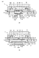
図1(a)は、この発明の第1の実施の形態に係る撮像素子モジュール11 を示すもので、撮像素子10は、その背面の絶縁シート101に赤外線反射部材である熱反射部材(低放射シート)11が接合されて、例えばセラミック製のパッケージ本体12内に収容配置される。この熱反射部材11は、例えばアルミニウム材で、鏡面仕上げ(放射率0.1以下)されて形成され、その表面に金属箔や金属酸化物や赤外線カットフィルタ(赤外線の反射率が高い)等がコーティング、あるいは樹脂シートに白色塗料(放射率が低い塗料)を塗布し、放射率が0.1から0.6以下で赤外線反射率75から90%の処理面が形成される。これにより、熱反射部材11は、撮像素子10からの熱を放熱板に伝熱すると外部(例えば、放熱板)から放射される赤外線を遮光し、赤外線の入射を阻止する。 1 (a) is shows the image sensor module 1 1 according to the first embodiment of the present invention, the imaging device 10, the heat reflecting member (low an infrared reflective member to the insulating sheet 101 in the back (Radiation sheet) 11 is joined and accommodated in, for example, a ceramic package body 12. The heat reflecting member 11 is made of, for example, an aluminum material and has a mirror finish (emissivity of 0.1 or less), and a metal foil, a metal oxide, an infrared cut filter (having high infrared reflectivity), or the like on the surface. A white paint (paint having a low emissivity) is applied to the coating or the resin sheet to form a treated surface with an emissivity of 0.1 to 0.6 and an infrared reflectivity of 75 to 90%. Thus, when the heat reflection member 11 transfers the heat from the image sensor 10 to the heat radiating plate, the heat radiating member 11 shields infrared rays radiated from the outside (for example, the heat radiating plate) and blocks the incidence of infrared rays.

上記放熱板の表面に黒色塗料、ジルコニア系セラミック、セラミック含有材料等の高放射率の塗料を塗布した放熱板と、この放熱板からの赤外線を熱反射部材(低放射率の樹脂シート)の表面で反射し、撮像素子の温度が再上昇することを抑制すると共に、放熱板の熱を空間(撮像素子付近の隙間等)に放熱することができる。   The surface of the above heat sink is coated with a high emissivity paint such as black paint, zirconia-based ceramic, ceramic-containing material, etc., and the surface of the heat reflecting member (low emissivity resin sheet) receives infrared rays from this heat sink , The temperature of the image sensor is prevented from rising again, and the heat of the heat sink can be radiated to a space (such as a gap near the image sensor).

上記パッケージ本体12には、放熱用開口部121が熱反射部材11に対向して設けられる。このパッケージ本体12は、その開口部121が、例えば弾性変形自在なフレキシブル印刷配線基板(以下、FPC基板と記す)13に設けられた放熱用開口部131に対向されて該FPC基板13に搭載されて熱的に結合される。そして、このパッケージ本体12は、そのリード端子122が、撮像素子10の電極とボンディング14で接続されている。このリード端子122は、外部に引き出されて上記FPC基板13の配線パターンに接続される。また、撮像素子10と電気的に接続されているリード端子122の配置される側部と、直交する両側部が、図2に示すように熱伝導性の優れた接着剤15を用いて上記FPC基板13に接着されて熱結合され、その上面部に保護ガラス16が被着されて撮像素子10が密閉収容される。   The package body 12 is provided with a heat radiation opening 121 facing the heat reflecting member 11. The package body 12 is mounted on the FPC board 13 so that the opening 121 is opposed to a heat radiation opening 131 provided on, for example, an elastically deformable flexible printed wiring board (hereinafter referred to as an FPC board) 13. And thermally coupled. The package body 12 has lead terminals 122 connected to the electrodes of the image sensor 10 by bonding 14. The lead terminal 122 is pulled out and connected to the wiring pattern of the FPC board 13. Further, the side portion where the lead terminal 122 electrically connected to the image pickup device 10 is disposed and the both side portions orthogonal to each other are bonded to each other using the adhesive 15 having excellent thermal conductivity as shown in FIG. The image pickup device 10 is hermetically accommodated by being bonded to the substrate 13 and thermally coupled, and having a protective glass 16 attached to the upper surface portion thereof.

上記FPC基板13には、例えば基板端部132が上記開口部131を挟んで設けられ、この基板端部132には、放熱部材を構成する第1の放熱部材17に設けられた突部171が対向されて上記パッケージ本体12と接合される。この第1の放熱部材17は、銅やアルミニウム合金等の金属材料で形成され、その略中央部に開口部170が上記FPC基板13の開口部131に対向して設けられる。ここで、パッケージ本体12は、第1の放熱部材17により位置決め支持される。   For example, a substrate end 132 is provided on the FPC board 13 with the opening 131 interposed therebetween, and a protrusion 171 provided on the first heat radiating member 17 constituting the heat radiating member is provided on the substrate end 132. It is opposed and joined to the package body 12. The first heat radiating member 17 is formed of a metal material such as copper or aluminum alloy, and an opening 170 is provided at a substantially central portion thereof so as to face the opening 131 of the FPC board 13. Here, the package body 12 is positioned and supported by the first heat radiating member 17.

上記第1の放熱部材17には、赤外線吸収部材である高放熱シート18が、上記放熱部材17の凹部131に位置するように設けられる。この高放熱シート18は、例えばアルミニウム材で形成して、その表面側に黒色アルマイト処理、スプライン加工、砂目処理(赤外線が反射しないように規則性あるいは不規則に凹凸を形成)等を施して0.9以上の放射率で、赤外線の反射率が低く熱吸収性を高めた処理面が形成され、開口部180が上記第2の放熱部材20の突起部170に挿通して設けられる。これにより、高放熱シート18は、外部または熱反射部材11からの赤外線を効率よく吸収して、熱反射部材への赤外線の放射を最小限に抑えることが可能となる。   The first heat radiating member 17 is provided with a high heat radiating sheet 18 as an infrared absorbing member so as to be positioned in the recess 131 of the heat radiating member 17. The high heat dissipation sheet 18 is formed of, for example, an aluminum material, and is subjected to black alumite treatment, spline processing, graining treatment (regular or irregular irregularities are formed so that infrared rays are not reflected), and the like. A treatment surface having an emissivity of 0.9 or more, a low infrared reflectance, and a high heat absorption property is formed, and an opening 180 is provided through the protrusion 170 of the second heat dissipation member 20. As a result, the high heat dissipation sheet 18 can efficiently absorb infrared rays from the outside or the heat reflecting member 11 and minimize infrared radiation to the heat reflecting member.

また、上記突起部170の上面に小孔を形成した開口部を形成し、熱反射部材11と高放熱シート18間に蓄積される熱を外部へ直接放射すると、放熱効率が向上する。   Further, when an opening having a small hole is formed on the upper surface of the protrusion 170 and the heat accumulated between the heat reflecting member 11 and the high heat dissipation sheet 18 is directly radiated to the outside, the heat dissipation efficiency is improved.

なお、上記高放熱シート18としては、例えば第1の放熱部材17の熱反射部材11に対向する部位に、上述した表面処理を施して、該第1の放熱部材17で直接的に構成するようにしても良い。   In addition, as the said high heat radiating sheet 18, the surface treatment mentioned above is given to the site | part which opposes the heat | fever reflection member 11 of the 1st heat radiating member 17, for example, and it is comprised directly by this 1st heat radiating member 17. Anyway.

また、第1の放熱部材17には、高放熱シート18の背面側に凹部172が設けられ、この凹部172に熱伝導材19を介在させて、突起部170および中空状の突部200を有した第2の放熱部材20が、例えばカシメ加工により圧着されて一体的に組みつけられる。この第2の放熱部材20は、例えば第1の放熱部材17と同材料で形成される。そして、熱伝導材19は、第1及び第2の放熱部材17,20より熱伝導性の優れたグラファイトカーボン材、シリコンゲル、金属発泡材、各種の多孔質結晶体、グラファイトシート等の材料で形成される。   Further, the first heat radiating member 17 is provided with a concave portion 172 on the back side of the high heat radiating sheet 18, and a thermal conductive material 19 is interposed in the concave portion 172, so that the projection 170 and the hollow projection 200 are provided. The second heat radiating member 20 is integrally assembled by being crimped by caulking, for example. The second heat radiating member 20 is made of the same material as that of the first heat radiating member 17, for example. The heat conductive material 19 is made of a material such as graphite carbon material, silicon gel, metal foam material, various porous crystals, graphite sheet, etc. having better heat conductivity than the first and second heat radiating members 17 and 20. It is formed.

これにより、熱反射部材11からの熱が高放熱シート18の開口部180から第2の放熱部材20の突起部170内を通り、外部に排熱されて、いわゆる熱の淀みがなくなり、撮像素子10の熱飽和の防止が図れる。   As a result, the heat from the heat reflecting member 11 passes through the inside of the protrusion 170 of the second heat radiating member 20 from the opening 180 of the high heat radiating sheet 18 and is exhausted to the outside. 10 thermal saturation can be prevented.

また、熱伝導体に代え、相変化材を用いた潜熱蓄熱材で、有機系として例えば、マイクロカプセル型パラフィン材料に炭素繊維を充填した有機材料からなる樹脂シートを形成してもよい。これにより、潜熱蓄熱材の相変化温度を40から50℃に設定すると、機器内の急激な温度上昇を抑制でき、温度センサによる温度異常検出を遅延することができるため、ユーザの利便性が良くなる。   Further, instead of the heat conductor, a latent heat storage material using a phase change material may be used, and as an organic system, for example, a resin sheet made of an organic material filled with carbon fibers in a microcapsule type paraffin material may be formed. Thereby, when the phase change temperature of the latent heat storage material is set to 40 to 50 ° C., rapid temperature rise in the device can be suppressed, and temperature abnormality detection by the temperature sensor can be delayed, which is convenient for the user. Become.

また、放熱部材17の下面を平坦(後述のカシメ加工が不要)とし、この放熱部材17にマイクロカプセル型パラフィン材料に炭素繊維を充填した有機材料からなる樹脂シートを接合すると、より放熱板17の構造が簡素で組み立ても容易となる。   Further, when the lower surface of the heat radiating member 17 is flat (no need for caulking processing described later) and a resin sheet made of an organic material filled with carbon fibers in a microcapsule-type paraffin material is joined to the heat radiating member 17, Simple structure and easy assembly.

上記第1の放熱部材17には、筐体結合部173が設けられ、この筐体結合部173は、例えば上記FPC基板13に設けられた挿通孔133に挿通されて機器筐体21に熱的に結合される。これにより、第1の放熱部材17は、熱移送された熱の一部を、機器筐体21に熱移送して該機器筐体21から放熱して撮像素子10の熱の上昇が抑制される。   The first heat radiating member 17 is provided with a housing coupling portion 173. The housing coupling portion 173 is inserted into an insertion hole 133 provided in the FPC board 13, for example, and is thermally applied to the device housing 21. Combined with As a result, the first heat radiating member 17 transfers a part of the heat transferred to the device housing 21 to dissipate the heat from the device housing 21 and suppresses an increase in the heat of the image sensor 10. .

また、上記FPC基板13には、例えばそのパッケージ本体12との接合部である上記接着剤15を挟んで4個の切り欠き部134が設けられ(図2参照)、この切り欠き部134には、上記第1の放熱部材17に立設した受熱部176が挿入される。この受熱部176は、上記高放熱シート18とは別にパッケージ本体12の周壁から放熱される熱を受熱する。   In addition, the FPC board 13 is provided with four notches 134 (see FIG. 2), for example, with the adhesive 15 that is a joint with the package body 12 interposed therebetween. The heat receiving portion 176 erected on the first heat radiating member 17 is inserted. The heat receiving portion 176 receives heat radiated from the peripheral wall of the package body 12 separately from the high heat dissipation sheet 18.

上記構成により、撮像素子10が駆動されて発熱すると、その熱は、そのパッケージ本体12及びFPC基板13から第1の放熱部材17に熱伝導により熱移送される。同時に、FPC基板13の他の電子部品からの熱が、該FPC基板13を介して第1の放熱部材17に熱伝導により熱移送される。   With the above configuration, when the image sensor 10 is driven to generate heat, the heat is transferred from the package body 12 and the FPC board 13 to the first heat radiating member 17 by heat conduction. At the same time, heat from other electronic components of the FPC board 13 is transferred by heat conduction to the first heat radiating member 17 through the FPC board 13.

なお、パッケージ本体12の下面と第1の放熱部材17との隙間から放出される熱がFPC基板に伝熱されないように、パッケージ本体12の一部を接着剤15で塞ぐことが望ましい。   In addition, it is desirable to block part of the package body 12 with the adhesive 15 so that heat released from the gap between the lower surface of the package body 12 and the first heat radiating member 17 is not transferred to the FPC board.

また、上記撮像素子10で発生した熱は、絶縁シート101を通して直接的に熱反射部材11に熱移送され、この熱反射部材11で赤外線として放射されて高放熱シート18を介して第1の放熱部材17に熱移送される。さらに、撮像素子10からの熱の一部は、パッケージ本体12の側壁から放熱される。この熱は、第1の放熱部材17の受熱部176に対流伝熱されて該第1の放熱熱部材17に熱移送される。   Further, the heat generated in the image pickup device 10 is directly transferred to the heat reflecting member 11 through the insulating sheet 101, and is radiated as infrared rays by the heat reflecting member 11 to be radiated through the high heat radiating sheet 18. Heat is transferred to the member 17. Further, a part of the heat from the image sensor 10 is radiated from the side wall of the package body 12. This heat is convectively transferred to the heat receiving portion 176 of the first heat radiating member 17 and transferred to the first heat radiating heat member 17.

このように3つの形態で第1の放熱部材17に熱移送された熱は、熱伝導材19を介して第2の放熱部材20に熱移送されて全体に効率よく熱伝導されて、その筐体結合部173より機器筐体21に熱移送されて外部に放熱され、ここに、撮像素子10が冷却されて所望の温度に熱が抑制される。この際、FPC基板13の他の搭載電子部品からの熱も排熱されて、該電子部品の冷却も行われる。   Thus, the heat transferred to the first heat radiating member 17 in three forms is transferred to the second heat radiating member 20 through the heat conducting material 19 and efficiently transferred to the entire heat transfer member. Heat is transferred from the body coupling portion 173 to the device casing 21 to be dissipated to the outside, and the image sensor 10 is cooled here to suppress heat to a desired temperature. At this time, heat from other mounted electronic components of the FPC board 13 is also exhausted, and the electronic components are also cooled.

このように、上記撮像素子モジュール11 は、機器筐体21に収容されるFPC基板13に開口部131を設けて、この開口部131に対して撮像素子10の絶縁シート101を対向させてFPC基板13に搭載し、その絶縁シート101に熱反射部材11を熱的に結合させて、この熱反射部材11に対向して機器筐体21及び撮像素子10の双方に熱的に結合される第1の放熱部材17を配置するように構成した。 Thus, the imaging device module 1 1 is an opening 131 provided on the FPC substrate 13 which is accommodated in the apparatus housing 21, are opposed to the insulating sheet 101 of the imaging device 10 with respect to the opening 131 FPC The heat reflecting member 11 is mounted on the substrate 13 and thermally coupled to the insulating sheet 101. The heat reflecting member 11 is thermally coupled to both the device casing 21 and the imaging element 10 so as to face the heat reflecting member 11. 1 radiating member 17 is arranged.

ここで、熱反射部材は、低放射シートなどの塗布された樹脂シートを用いた場合には、絶縁シート101を省くことができる。   Here, the insulating sheet 101 can be omitted as the heat reflecting member when an applied resin sheet such as a low radiation sheet is used.

これによれば、FPC基板13に半田付けされた撮像素子10の熱は、その絶縁シート101から熱反射部材11に熱移送される。その後、熱移送された熱の一部は、熱反射部材11からFPC基板13の半田付け面と逆側に配置した第1の放熱部材17に接合された高放熱シート18や突起部170の内部へと赤外線を放出して熱移送される。さらに、熱反射部材11に伝導された熱は、パッケージ本体12からFPC基板13や受熱部176に熱伝導されて第1の放熱部材17に熱伝導される。   According to this, the heat of the image sensor 10 soldered to the FPC board 13 is transferred from the insulating sheet 101 to the heat reflecting member 11. Thereafter, a part of the heat transferred is transferred from the heat reflecting member 11 to the first heat radiating member 17 disposed on the side opposite to the soldering surface of the FPC board 13 and inside the high heat radiating sheet 18 and the protrusion 170. Infrared rays are emitted to the heat transfer. Further, the heat conducted to the heat reflecting member 11 is conducted from the package body 12 to the FPC board 13 and the heat receiving unit 176 and conducted to the first heat radiating member 17.

また、図1(b)は、この発明の第1の実施の形態に係る撮像素子モジュールの他の構成例を示した断面図である。   FIG. 1B is a cross-sectional view showing another configuration example of the image sensor module according to the first embodiment of the present invention.

図1(a)と異なる点は、第1の放熱部材17に、熱伝導材171a、第3の放熱部材171b、熱伝導材19、第2の放熱部材20及び放熱シート20aが積層状に設けられて、突起部170が設けられていないことである。上記放熱シート20aは、セラミック含有材料が第2の放熱部材20の表面に塗布されることによって形成されるもので、放熱した熱を空間に放出するために設けられている。   The difference from FIG. 1A is that the first heat radiating member 17 is provided with a heat conductive material 171a, a third heat radiating member 171b, a heat conductive material 19, a second heat radiating member 20, and a heat radiating sheet 20a in a laminated form. In other words, the protrusion 170 is not provided. The heat radiating sheet 20a is formed by applying a ceramic-containing material on the surface of the second heat radiating member 20, and is provided to release the radiated heat to the space.

このように、第1の放熱部材17を2部品に分解し、熱伝導体171aを両部品の境界部に介在させ、放熱シート20aを表面に貼り付けることで、より高い放熱効率を得ることができ、放熱板の小型化が可能となる。   Thus, by disassembling the first heat radiating member 17 into two parts, interposing the heat conductor 171a at the boundary between both parts, and attaching the heat radiating sheet 20a to the surface, higher heat radiation efficiency can be obtained. This makes it possible to reduce the size of the heat sink.

また、上記撮像素子はパッケージ型のタイプについて説明したが、ベアチップ型のタイプに置き換えることも可能である。   In addition, although the image pickup element has been described as a package type, it can be replaced with a bare chip type.

次に、上記撮像素子モジュールの使用形態について説明する。なお、ここでは、一例として、図1(b)に示す構成の撮像素子モジュール1を例として説明する。   Next, a usage pattern of the image sensor module will be described. Here, as an example, the imaging element module 1 having the configuration shown in FIG. 1B will be described as an example.

例えば上記撮像素子モジュール1は、図3に示すように携帯用電子機器である電子カメラのレンズユニット50とカメラ本体51との間に組付けられて使用に供される。但し、この図3においては、上記図1及び図2と同一部分について、同一符合を付して詳細な説明を省略する。   For example, as shown in FIG. 3, the imaging element module 1 is assembled between a lens unit 50 and a camera body 51 of an electronic camera that is a portable electronic device, and is used. However, in FIG. 3, the same parts as those in FIGS. 1 and 2 are given the same reference numerals, and detailed description thereof is omitted.

即ち、上記撮像素子モジュール1は、ユニット接続環52に収容され、その第1の放熱部材17が上記ユニット接続環52に熱的に結合される。そして、このユニット接続環52は、その基端がカメラ本体51に螺子部材53を用いて螺着される。そして、この撮像素子モジュール1の上面には、例えば図4に示す防塵機構54が組付けられる。   That is, the image sensor module 1 is accommodated in the unit connection ring 52, and the first heat radiating member 17 is thermally coupled to the unit connection ring 52. The base end of the unit connection ring 52 is screwed to the camera body 51 using a screw member 53. For example, a dustproof mechanism 54 shown in FIG. 4 is assembled on the upper surface of the imaging element module 1.

この防塵機構54は、ローパスフィルタ541が取付け部材542に設けられた開口部543を閉塞するように設けられ、このローパスフィルタ541は、環形状したゴム材の支持板544を介して上記撮像素子10の上面に配置される。そして、取付け部材542は、そのローパスフィルタ541が上記撮像素子10上に支持板544を介して対向配置された状態で、上記パッケージ本体12に対して螺子部材545を用いて、図示されていないが、機器筐体21に螺着されて配置される。これにより、パッケージ本体12の保護ガラス16の表面への塵埃の侵入を防止することができる。   The dust-proof mechanism 54 is provided so that the low-pass filter 541 closes the opening 543 provided in the mounting member 542, and the low-pass filter 541 is connected to the imaging element 10 via the ring-shaped rubber material support plate 544. It is arranged on the upper surface. The mounting member 542 is not shown in the drawing using a screw member 545 with respect to the package body 12 in a state where the low-pass filter 541 is disposed on the imaging element 10 via a support plate 544. The device casing 21 is screwed and arranged. Thereby, the penetration | invasion of the dust to the surface of the protective glass 16 of the package main body 12 can be prevented.

また、取付け部材542には、ローパスフィルタ541に対向して防塵用の透明ガラス基板546が所定の間隔を有して配置され、この透明ガラス基板546は、弾性部材547を介在して螺子部材548を用いて所望の気密性を有して閉塞されて組付けられる。そして、この透明ガラス基板546と取付け部材542との間には、圧電素子等の加振部材549と、ローパスフィルタ541の表面への塵埃の侵入を防止するために環状に形成されたゴム部材550(ここではOリングとしたが、加振部材549の幅と同一幅でもよい)が介在される。   In addition, a dust-proof transparent glass substrate 546 is disposed on the attachment member 542 so as to face the low-pass filter 541 with a predetermined interval. The transparent glass substrate 546 is interposed between the screw member 548 with an elastic member 547 interposed therebetween. Is closed and assembled with a desired airtightness. Between the transparent glass substrate 546 and the mounting member 542, a vibration member 549 such as a piezoelectric element and a rubber member 550 formed in an annular shape to prevent dust from entering the surface of the low-pass filter 541 are provided. (Here, it is an O-ring, but it may be the same width as the vibration member 549).

ここで、透明ガラス基板546は、ローパスフィルタ541に対して気密を有して振動可能に対向配置され、加振部材549が図示しない駆動制御部を介して駆動されて加振されると、その振動が伝達される。すると、透明ガラス基板546は、弾性部材547の弾性力に抗して気密を保った状態で振動され、その表面等に付着した塵等を除去して、ローパスフィルタ541内への塵の侵入を阻止する。   Here, the transparent glass substrate 546 is arranged to face the low-pass filter 541 in an airtight manner so as to vibrate, and when the vibration member 549 is driven and vibrated via a drive control unit (not shown), Vibration is transmitted. Then, the transparent glass substrate 546 is vibrated in an airtight state against the elastic force of the elastic member 547 to remove dust and the like adhering to the surface of the transparent glass substrate 546 and prevent the dust from entering the low-pass filter 541. Stop.

上記ユニット接続環52の先端部には、上記レンズユニット50が組付けられる。このレンズユニット50には、撮像レンズ系が収納配置される。この撮像レンズ系は、例えば第1群の第1のレンズ55a、第2群の第2及び第3のレンズ55b,55c、第3群の第4のレンズ25dの3群4枚で構成され、その第2群の第2及び第3のレンズ55b,55cを光軸O方向に移動させて焦点調節が行われる。   The lens unit 50 is assembled to the tip of the unit connection ring 52. In this lens unit 50, an imaging lens system is accommodated. The imaging lens system includes, for example, four lenses in three groups: a first lens 55a in the first group, second and third lenses 55b and 55c in the second group, and a fourth lens 25d in the third group. Focus adjustment is performed by moving the second and second lenses 55b and 55c in the second group in the direction of the optical axis O.

上記第1のレンズ55aと、第4のレンズ55dは、それぞれホルダ56a,56dに収容され、このホルダ56a,56dを介して光軸上に位置決め固定されて配置される。そして、第2及び第3のレンズ55b、55cは、ホルダ56bに収容され、このホルダ56bは、例えばガタ防止構造を有した案内機構57に光軸に対応した矢印A,B方向に移動自在に支持される。   The first lens 55a and the fourth lens 55d are accommodated in holders 56a and 56d, respectively, and are positioned and fixed on the optical axis via the holders 56a and 56d. The second and third lenses 55b and 55c are accommodated in a holder 56b. The holder 56b is movable in the directions of arrows A and B corresponding to the optical axis, for example, in a guide mechanism 57 having a backlash prevention structure. Supported.

このホルダ56bは、直線螺子機構58に光軸方向の矢印A,B方向に直線移動自在に連結される。この直線螺子機構58は、例えばステッピングモータ59に駆動自在に連結され、このステッピングモータ59の駆動に連動して回転駆動されて、上記ホルダ56aを矢印A,B方向に直線移動される。この際、ホルダ56bは、上記案内機構57に案内されて矢印A,B方向に移動されて、上記第2及び第3のレンズ55b,55cを光軸方向に移動させて焦点調整を実行する。   The holder 56b is coupled to the linear screw mechanism 58 so as to be linearly movable in the directions of arrows A and B in the optical axis direction. The linear screw mechanism 58 is connected to, for example, a stepping motor 59 so as to be freely driven, and is rotationally driven in conjunction with the driving of the stepping motor 59 to linearly move the holder 56a in the directions of arrows A and B. At this time, the holder 56b is guided by the guide mechanism 57 and moved in the directions of arrows A and B, and the focus adjustment is performed by moving the second and third lenses 55b and 55c in the optical axis direction.

このように上記撮像素子モジュール1は、電子カメラのレンズユニット50に組付けることで、上述したように高効率な冷却を実現したうえで、その熱設計を含む製作の自由度の向上が図れるため、そのカメラ本体51の小形化に寄与することが可能となる。   As described above, the imaging device module 1 is assembled in the lens unit 50 of the electronic camera, so that the highly efficient cooling can be realized as described above, and the manufacturing flexibility including the thermal design can be improved. It is possible to contribute to downsizing of the camera body 51.

なお、上記第1の実施の形態では、弾性変形自在なFPC基板13を用いて構成した場合について説明したが、これに限ることなく、その他、ハードタイプの印刷配線基板を用いて構成することも可能で、同様に有効な効果が期待される。   In the first embodiment, the case where the elastically deformable FPC board 13 is used has been described. However, the invention is not limited to this, and a hard type printed wiring board may also be used. It is possible and expected to be effective as well.

また、この発明は、上記第1の実施の形態に限ることなく、その他、例えば図5、図6、図7、図8、図9及び図10、図11にそれぞれ示すように撮像素子モジュール1a、1b、1c、1d、1e、1fを構成してよく、同様に有効な効果を期待することができる。但し、図5乃至図11においては、上記図1及び図2と同一部分について同一符号を付して、その詳細な説明を省略する。   In addition, the present invention is not limited to the first embodiment, and other components such as the image sensor module 1a as shown in FIGS. 5, 6, 7, 8, 9, 10 and 11, for example. 1b, 1c, 1d, 1e, and 1f may be configured, and similarly effective effects can be expected. However, in FIG. 5 to FIG. 11, the same parts as those in FIG. 1 and FIG.

図5に示す撮像素子モジュール1aは、上記撮像素子10をパッケージ本体12に収容したパッケージタイプに適用したもので、このパッケージ本体12の底面に撮像素子10の絶縁シート101に対応して開口部121を形成する。そして、この開口部121には、上記撮像素子10の絶縁シート101に接合した赤外線反射部材である上記熱反射部材11が配置される。   An image sensor module 1a shown in FIG. 5 is applied to a package type in which the image sensor 10 is accommodated in a package body 12. An opening 121 corresponding to the insulating sheet 101 of the image sensor 10 is formed on the bottom surface of the package body 12. Form. In the opening 121, the heat reflecting member 11 that is an infrared reflecting member bonded to the insulating sheet 101 of the imaging element 10 is disposed.

また、上記撮像素子10が搭載されたFPC基板13には、開口部131が上記パッケージ本体12の開口部121に連続して形成される。そして、このパッケージ本体12の開口部121及び上記FPC基板13の開口部131には、アルミニウム合金等の金属材料製の放熱部材60の一端部に設けられる凹状の第1の熱結合部601が挿通されて、該第1の熱結合部601の先端部が、上記撮像素子10の絶縁シート101と熱的に結合される。   An opening 131 is continuously formed in the opening 121 of the package body 12 in the FPC board 13 on which the imaging element 10 is mounted. A concave first heat coupling portion 601 provided at one end of a heat radiating member 60 made of a metal material such as an aluminum alloy is inserted into the opening 121 of the package body 12 and the opening 131 of the FPC board 13. As a result, the tip of the first thermal coupling portion 601 is thermally coupled to the insulating sheet 101 of the image sensor 10.

上記放熱部材60の第1の熱結合部601には、その内壁に放熱フィン602が形成され、その底面に高放熱シート18aが、上記熱反射部材11に対向して配置される。それと共に、高放熱シート18が、FPC基板13に沿って延出して配置される。これにより、この高放熱シート18aは、上記熱反射部材11から放射される赤外線を受熱して第1の熱結合部601に熱移送する。   The first heat coupling portion 601 of the heat radiating member 60 has heat radiating fins 602 formed on the inner wall thereof, and a high heat radiating sheet 18a is disposed on the bottom surface thereof so as to face the heat reflecting member 11. At the same time, the high heat dissipation sheet 18 extends along the FPC board 13. As a result, the high heat dissipation sheet 18 a receives the infrared rays emitted from the heat reflecting member 11 and transfers the heat to the first heat coupling portion 601.

また、上記第1の熱結合部601には、幅広な第2の熱結合部603が着脱可能に設けられる。この第2の熱結合部603は、その幅広部位が上記FPC基板13の背面側に熱的に結合される。   The first thermal coupling portion 601 is detachably provided with a wide second thermal coupling portion 603. The wide portion of the second thermal coupling portion 603 is thermally coupled to the back side of the FPC board 13.

第2の熱結合部603には、例えば内外壁に放熱フィンが突設された中空部604が設けられ、この中空部604内には、例えば上述した熱伝導性の優れたグラファイトカーボン材、シリコンゲル、金属発泡材、各種の多孔質結晶体、グラファイトシート等の熱伝導材19や無機または有機系の潜熱蓄熱材が密閉収容される。これにより、放熱部材60は、十分な放熱面積が得られ、第1の熱結合部601に熱が移送されると、その熱伝導材19を経由して、第2の熱結合部603を含む全体に効率よく熱伝導され、高効率な放熱が実現できる。   The second thermal coupling portion 603 is provided with, for example, a hollow portion 604 in which heat radiating fins are projected on inner and outer walls. In the hollow portion 604, for example, the above-described graphite carbon material having excellent thermal conductivity, silicon The heat conductive material 19 such as gel, metal foam material, various porous crystals, graphite sheet, and inorganic or organic latent heat storage material are hermetically contained. Thereby, the heat radiating member 60 has a sufficient heat radiating area, and when heat is transferred to the first thermal coupling portion 601, the second thermal coupling portion 603 is included via the thermal conductive material 19. The whole is efficiently heat-conductive and high-efficiency heat dissipation can be realized.

また、図6に示す撮像素子モジュール1bは、いわゆるベアチップタイプの撮像素子10aを用いて構成したもので、FPC基板13には、撮像素子10aの絶縁シート101aに対応して開口部131を形成する。そして、この開口部131には、上記撮像素子10aの絶縁シート101aに上記赤外線反射部材である熱反射部材11が接合されて配置される。   The imaging element module 1b shown in FIG. 6 is configured using a so-called bare chip type imaging element 10a, and an opening 131 is formed in the FPC board 13 corresponding to the insulating sheet 101a of the imaging element 10a. . And in this opening part 131, the heat | fever reflection member 11 which is the said infrared reflection member is joined and arrange | positioned at the insulating sheet 101a of the said image pick-up element 10a.

さらに、上記撮像素子10aが搭載されたFPC基板13の背面には、支持部材を構成する第1の放熱部材62が熱的に結合されて積重配置される。この第1の放熱部材62には、開口部621が上記熱反射部材11に対向して形成され、この開口部621には、例えば銅等の金属材料製の凹状の第2の放熱部材63が、上記熱反射部材11に対向して、例えば螺子部材64を用いて螺着される。   Further, a first heat radiating member 62 constituting a support member is thermally coupled and stacked on the back surface of the FPC board 13 on which the imaging element 10a is mounted. An opening 621 is formed in the first heat radiating member 62 so as to face the heat reflecting member 11, and a concave second heat radiating member 63 made of a metal material such as copper is formed in the opening 621. For example, a screw member 64 is used to face the heat reflecting member 11.

この第2の放熱部材63には、例えばその側壁に排気孔631が設けられ、その底面外壁には、放熱フィン632が形成される。これにより、第2の放熱部材63は、その排気孔631及び放熱フィン632を介して熱移送された熱を外部に効率よく排熱することができる。   The second heat radiating member 63 is provided with, for example, exhaust holes 631 on the side wall thereof, and heat radiating fins 632 are formed on the bottom outer wall thereof. Thus, the second heat radiating member 63 can efficiently exhaust the heat transferred through the exhaust holes 631 and the heat radiating fins 632 to the outside.

第2の放熱部材63には、その内部に例えば金属材料製の第3の放熱部材65が、紫外線硬化型接着剤を用いて接合されて収容配置される。この第3の放熱部材65には、その周壁に放熱フィン651が設けられ、この放熱フィン651に先端部が第2の放熱部材63の内壁に熱的に結合されている。そして、この第3の放熱部材65には、例えば排気孔652が上記第2の放熱部材63の排気孔631に対応して設けられ、この排気孔652を通して熱移送された熱を外部に効率よく排熱することができる。   In the second heat radiating member 63, for example, a third heat radiating member 65 made of a metal material is joined and disposed by using an ultraviolet curable adhesive. The third heat radiating member 65 is provided with a heat radiating fin 651 on its peripheral wall, and the tip of the heat radiating fin 651 is thermally coupled to the inner wall of the second heat radiating member 63. The third heat radiating member 65 is provided with, for example, an exhaust hole 652 corresponding to the exhaust hole 631 of the second heat radiating member 63, and the heat transferred through the exhaust hole 652 is efficiently transferred to the outside. Heat can be exhausted.

また、上記第1の放熱部材62には、突起部622が設けられ、この突起部622が上記FPC基板13の挿通孔132に挿通されて、機器筐体66に熱的に結合される。これにより、第1の放熱部材62は、撮像素子10a及びFPC基板13を介して熱移送された熱を機器筐体66に熱移送して排熱することができる。   The first heat radiating member 62 is provided with a protrusion 622, and the protrusion 622 is inserted into the insertion hole 132 of the FPC board 13 and is thermally coupled to the device housing 66. As a result, the first heat radiating member 62 can transfer the heat transferred through the imaging element 10a and the FPC board 13 to the device housing 66 to exhaust the heat.

なお、上記第1乃至第3の放熱部材62,63,65は、例えば同一金属材料で形成される。   The first to third heat radiating members 62, 63, 65 are made of, for example, the same metal material.

また、図7に示す撮像素子モジュール1cは、手振れ補正を有する一眼レフレックスデジタルカメラに適用される。したがって、撮像素子はカメラ本体によって撮影レンズの光軸に直交するXY平面上に変位可能な状態で支持され、撮影時に手振れ補正機構(例えば、駆動コイルと永久磁石で構成されたリニアモータやステップモータとネジ軸の構成による電磁駆動、あるいは圧電素子や屈曲振動子を用いたリニアモータなど)により手振れ状態に対応してXY平面を駆動される。上記ベアチップタイプの撮像素子10aを用いて構成したもので、FPC基板13には、撮像素子10aが、その絶縁シート101aが基板面に対向して搭載される。このFPC基板13には、開口部131が絶縁シート101aに対向して設けられ、この開口部131には、上記熱反射部材11が接合される。   Further, the image sensor module 1c shown in FIG. 7 is applied to a single-lens reflex digital camera having camera shake correction. Therefore, the image pickup device is supported by the camera body in a state in which it can be displaced on the XY plane orthogonal to the optical axis of the photographing lens, and a camera shake correction mechanism (for example, a linear motor or a step motor composed of a drive coil and a permanent magnet) at the time of photographing. The XY plane is driven in response to the hand shake state by electromagnetic drive using a screw shaft configuration or a linear motor using a piezoelectric element or a bending vibrator. The bare chip type image pickup device 10a is used, and the image pickup device 10a is mounted on the FPC board 13 with the insulating sheet 101a facing the substrate surface. An opening 131 is provided in the FPC board 13 so as to face the insulating sheet 101 a, and the heat reflecting member 11 is joined to the opening 131.

このFPC基板13は、例えば金属材料で形成される第1の放熱部材67に積重され、この第1の放熱部材67により支持されて配置される。この第1の放熱部材67には、開口部671が上記FPC基板13の開口部131に対向して形成され、この第1の放熱部材67の開口部671には、例えば金属材料で形成される凹状の第2の放熱部材68の先端部が熱的に結合されて取付けられる。   The FPC board 13 is stacked on a first heat radiating member 67 made of, for example, a metal material, and is supported and arranged by the first heat radiating member 67. An opening 671 is formed in the first heat radiating member 67 so as to face the opening 131 of the FPC board 13, and the opening 671 of the first heat radiating member 67 is formed of, for example, a metal material. The tip of the concave second heat radiating member 68 is attached by being thermally coupled.

この第2の放熱部材68は、その中間部にヒートパイプタイプの、いわゆるウィック管である周知の板状の金属管69が熱的に結合されて閉塞される。金属管69には、その一方の面に上述した赤外線の反射率が低く熱吸収性を高めた処理面を有する高放熱シート18が、上記熱反射部材11に対向して配置される。   The second heat radiating member 68 is closed by thermally coupling a known plate-like metal tube 69, which is a so-called wick tube, to the middle portion thereof. In the metal tube 69, the high heat dissipation sheet 18 having a treatment surface with low infrared reflectance and high heat absorption is disposed on one surface of the metal tube 69 so as to face the heat reflecting member 11.

また、第2の放熱部材68には、内壁に案内溝681が設けられ、この案内溝681には、銅材等の金属材料製の金属板70が、上記金属管69との間に上記シリコンゲル、グラファイトシート材等の熱伝導材19が介在されて移動自在に組付けられる。金属板70には、上記第2の放熱部材68の底部に螺合調整自在に設けられた調整螺子部材71の先端部が係合され、この調整螺子部材71の螺合調整により、昇降移動されて熱伝導材19を挟んで上記金属管69に圧接される。   The second heat radiating member 68 is provided with a guide groove 681 on the inner wall, and a metal plate 70 made of a metal material such as a copper material is interposed between the silicon tube 69 and the silicon tube 69 in the guide groove 681. A heat conductive material 19 such as a gel or a graphite sheet material is interposed, and is assembled to be movable. The metal plate 70 is engaged with a leading end portion of an adjusting screw member 71 provided so as to be screwed and adjustable at the bottom of the second heat radiating member 68, and is moved up and down by adjusting the screwing of the adjusting screw member 71. Thus, the metal pipe 69 is pressed against the heat conductive material 19.

この際、熱伝導材19は、金属板70に設けられた空気抜き孔701によりその内部空気が抜けて金属管69と金属板70との間に挟装される。これにより、金属管69と第2の放熱部材68との間は、熱伝導材19及び金属板70を介して効率的な熱伝導を可能とり、高効率な熱伝導が可能となる。   At this time, the heat conducting material 19 is sandwiched between the metal tube 69 and the metal plate 70 through the air vent holes 701 provided in the metal plate 70 so that the internal air is released. Thereby, efficient heat conduction is possible between the metal pipe 69 and the second heat radiating member 68 via the heat conducting material 19 and the metal plate 70, and highly efficient heat conduction is possible.

なお、上記金属管69は、接続管692を介して循環路を構成する例えば可撓性合成樹脂管72に接続される。この可撓性合成樹脂管72には、図示しない機器本体側のシャーシに配置された凝縮器及び圧電ポンプに順に配管接続され、このウイック付きヒートパイプや圧電ポンプにより、純水、アルコール、相変化媒体等の作動流体が上記金属管69および凝縮器に循環供給されて撮像素子から熱移送された熱の排熱を実現する。この場合、上記作動流体は、撮像素子10aの発熱温度の飽和温度に対する最適な沸点のものに設定することが好ましい。   The metal pipe 69 is connected to, for example, a flexible synthetic resin pipe 72 that constitutes a circulation path via a connection pipe 692. The flexible synthetic resin pipe 72 is connected in order to a condenser and a piezoelectric pump arranged in a chassis (not shown) on the equipment body side, and pure water, alcohol, phase change is performed by the heat pipe with the wick or the piezoelectric pump. A working fluid such as a medium is circulated and supplied to the metal tube 69 and the condenser to realize exhaust heat of the heat transferred from the image sensor. In this case, the working fluid is preferably set to have an optimum boiling point with respect to the saturation temperature of the heat generation temperature of the image sensor 10a.

また、上記第1の放熱部材67は、熱結合部672が設けられ、この熱結合部672は、上記FPC基板13に設けられた挿通孔132に挿通されて上記機器筐体66に熱的に結合される。これにより、第1の放熱部材67は、撮像素子10aを含むFPC基板13より熱移送された熱を、その熱結合部672を介して機器筐体66に熱移送して排熱することができる。   The first heat radiating member 67 is provided with a thermal coupling portion 672, and the thermal coupling portion 672 is inserted into the insertion hole 132 provided in the FPC board 13 and thermally connected to the device housing 66. Combined. As a result, the first heat radiating member 67 can exhaust the heat transferred from the FPC board 13 including the imaging element 10a to the device housing 66 through the heat coupling portion 672 and exhaust the heat. .

なお、上記第1及び第2の放熱部材67,68、金属板70は、例えば同一材料で形成される。   The first and second heat radiation members 67 and 68 and the metal plate 70 are made of the same material, for example.

また、図8に示す撮像素子モジュール1d(図7と同様に手振れ補正機能を有する一眼レフレックスデジタルカメラに適用)は、上記ベアチップタイプの撮像素子10aを用いて構成したもので、FPC基板13には、開口部131が撮像素子10aの絶縁シート101aに対向して設けられ、この開口部131には、例えば上記放射率が0.1以下の処理面を有した熱反射部材11が接合される。   An image sensor module 1d shown in FIG. 8 (applied to a single-lens reflex digital camera having a camera shake correction function as in FIG. 7) is configured using the bare-chip type image sensor 10a. The opening 131 is provided to face the insulating sheet 101a of the image pickup device 10a, and the heat reflecting member 11 having, for example, a processing surface having an emissivity of 0.1 or less is joined to the opening 131. .

FPC基板13は、銅材等の金属材料製の基板保持部を構成する第1の放熱部材73に載置されて熱的に結合され、この第1の放熱部材73により保持された状態で、該第1放熱部材73を包み込むように折返されて、例えば銅等の金属材料製の押え部材74に沿うように係合されて位置決めされる。この押え部材74には、突部741が形成され、この突部741が上記FPC基板13に挿通されて上記第1の放熱部材73に対して面接触され、熱的に結合される。   The FPC board 13 is placed on and thermally coupled to the first heat radiating member 73 that constitutes the board holding portion made of a metal material such as copper, and is held by the first heat radiating member 73. The first heat dissipating member 73 is folded back so as to be engaged and positioned so as to follow a presser member 74 made of a metal material such as copper. A protrusion 741 is formed on the pressing member 74, and the protrusion 741 is inserted into the FPC board 13 and brought into surface contact with the first heat radiating member 73 to be thermally coupled.

第1の放熱部材73には、例えば上記FPC基板13の開口部131が収容可能な筒状に形成され、その内壁部には、案内溝731が設けられる。そして、この案内溝731には、金属材料製の第2の放熱部材75及び第3の放熱部材76が、例えば上記シリコンゲル、グラファイトシート等で構成される熱伝導材19を挟んで接合された状態で、移動自在に収容される。   The first heat radiating member 73 is formed in a cylindrical shape that can accommodate the opening 131 of the FPC board 13, for example, and a guide groove 731 is provided on the inner wall thereof. Then, the second heat radiating member 75 and the third heat radiating member 76 made of a metal material are joined to the guide groove 731 with the heat conductive material 19 made of, for example, the above-described silicon gel, graphite sheet or the like interposed therebetween. In a state, it is accommodated movably.

これら第2及び第3の放熱部材75,76には、それぞれ対向する一方面に放熱フィン751,761が設けられ、この各放熱フィン751,761が熱伝導材19を介して熱的に結合されている。そして、これら第2及び第3の放熱部材75,76は、例えばその第3の放熱部材76の一部が、上記第1の放熱部材73に螺子部材77を用いて螺着されて該第1の放熱部材73内に収容配置される。なお、第2の放熱部材75上の熱本社部材11と対向する面には、高放熱シート75aが接合されている。   The second and third heat radiating members 75 and 76 are provided with heat radiating fins 751 and 761 on one side facing each other, and the heat radiating fins 751 and 761 are thermally coupled via the heat conducting material 19. ing. The second and third heat radiating members 75, 76 are, for example, a part of the third heat radiating member 76 is screwed to the first heat radiating member 73 using a screw member 77. The heat radiating member 73 is accommodated and disposed. A high heat dissipation sheet 75 a is joined to the surface of the second heat dissipation member 75 facing the thermal head office member 11.

また、上記FPC基板13には、例えば温度センサ78が搭載され、この温度センサ78で上記第1の放熱部材73内の温度が検出される。この温度センサ78は、第1の放熱部材73内の周囲温度を検出して図示しない制御部に出力する。この制御部(図示せず)は、温度センサ78の検出信号に基づいて、その温度が所定時間以上、所定の温度以上であるのを検出した状態で、危険信号を生成して図示しない表示部に動作停止等の危険を表示したりする。   Further, for example, a temperature sensor 78 is mounted on the FPC board 13, and the temperature in the first heat radiating member 73 is detected by the temperature sensor 78. The temperature sensor 78 detects the ambient temperature in the first heat radiating member 73 and outputs it to a control unit (not shown). This control unit (not shown) generates a danger signal based on the detection signal of the temperature sensor 78 and detects that the temperature is higher than the predetermined temperature for a predetermined time or more, and displays a display unit (not shown). Display a danger such as operation stop.

さらに、上記撮像素子10aには、例えばその撮像面の周囲部に、例えば周知の手振れ防止機構を構成する移動枠79に支持された押え部材80が係合され、その面方向が一定に維持された状態で、移動枠79を介して二次元的に移動されて、いわゆる手振れ補正が可能に構成される。この移動枠79は、例えば図示しない結合手段を介して上記押え部材74に熱的に結合され、その駆動に伴う熱が結合手段を介して上記押え部材74、第1の放熱部材73に熱移送されて排熱される。   Furthermore, for example, a pressing member 80 supported by a moving frame 79 constituting a known camera shake prevention mechanism is engaged with the imaging element 10a, for example, around the imaging surface, and the surface direction is maintained constant. In this state, the image is moved two-dimensionally via the moving frame 79, and so-called camera shake correction is possible. The moving frame 79 is thermally coupled to the pressing member 74 through, for example, a coupling means (not shown), and heat accompanying driving thereof is transferred to the pressing member 74 and the first heat radiating member 73 through the coupling means. Is exhausted.

ここで、図8中、762は、例えば上記第3の放熱部材76に設けられ、上記第2の放熱部材75と熱伝導材19を介在させて接合する際の熱伝導材19の内部空気を排出するための空気抜き孔である。   Here, in FIG. 8, 762 is provided in the third heat radiating member 76, for example, and the internal air of the heat conductive material 19 when the second heat radiating member 75 and the heat conductive material 19 are joined. It is an air vent hole for discharging.

この実施の形態においては、上記第2の放熱部材75の他方面に、例えば上述した赤外線の反射率が低く熱吸収性を高めた処理面を有した高放熱シート18を、上記熱反射部材11に対向して配置することで、さらに良好な熱移送特性を得ることが期待できる。   In this embodiment, the heat radiating member 11 is provided with the high heat radiating sheet 18 having, for example, the above-described treatment surface with low infrared reflectance and high heat absorption on the other surface of the second heat radiating member 75. It can be expected that better heat transfer characteristics can be obtained by disposing them facing each other.

また、図9に示す撮像素子モジュール1eは、上記図8に示す実施の形態において、第1及び第2の放熱部材75,76に周知のウィックタイプのヒートパイプ81を熱的に結合させて組付けて、このヒートパイプ81で上記FPC基板13の開口部131を通して上記撮像素子10aの絶縁シート101aに熱的に結合された熱反射部材11からの放射された赤外線を受光するように構成したものである。そこで、図9の説明においては、上記図8と同一部分について同一符号を付して、その詳細な説明を省略する。   Further, in the embodiment shown in FIG. 8, the imaging element module 1e shown in FIG. 9 is assembled by thermally connecting a well-known wick type heat pipe 81 to the first and second heat radiating members 75 and 76. In addition, the heat pipe 81 is configured to receive infrared rays emitted from the heat reflecting member 11 thermally coupled to the insulating sheet 101a of the imaging element 10a through the opening 131 of the FPC board 13. It is. Therefore, in the description of FIG. 9, the same parts as those in FIG. 8 are denoted by the same reference numerals, and detailed description thereof is omitted.

上記ヒートパイプ81は、作動流体が内蔵された循環路で形成され、その中間部に、例えば特開2003−28068号公報等に開示されている周知の圧電型ポンプ82が、図9の要部を拡大して示した一部断面図である図10に示すように、封止弁83を介在して配管接続される。この圧電型ポンプ82は、例えば上記FPC基板13に搭載され、封止弁83が図示しない制御部を介して駆動制御されると、作動流体が循環供給され、上記熱反射部材11から放射される熱を受熱して第1及び第2の放熱部材75,76に熱移送して放熱を実現する。   The heat pipe 81 is formed of a circulation path in which a working fluid is incorporated, and a known piezoelectric pump 82 disclosed in, for example, Japanese Patent Application Laid-Open No. 2003-28068 is provided in the middle part of FIG. As shown in FIG. 10 which is a partial cross-sectional view showing an enlarged view, the pipe connection is made with a sealing valve 83 interposed therebetween. The piezoelectric pump 82 is mounted on, for example, the FPC board 13. When the sealing valve 83 is driven and controlled via a control unit (not shown), the working fluid is circulated and supplied and radiated from the heat reflecting member 11. Heat is received and transferred to the first and second heat radiating members 75 and 76 to realize heat radiation.

ところで、上記撮像素子モジュール1eは、電子カメラに用いた場合、使用者が撮影モードを切替えたり、電源動作開始時において、撮像素子10a近傍に温度が所定値以上となると、図示しない制御部が上記圧電型ポンプ82を駆動するように構成される。この圧電型ポンプ82が駆動されると、作動流体が循環路に循環され、第2の放熱部材75、熱伝導材19、第3の放熱部材76に熱移送され、撮像素子10a近傍の温度上昇が抑制される。   By the way, when the image sensor module 1e is used in an electronic camera, when the user switches the shooting mode or the temperature of the image sensor 10a exceeds a predetermined value at the start of power supply operation, a control unit (not shown) The piezoelectric pump 82 is configured to be driven. When this piezoelectric pump 82 is driven, the working fluid is circulated through the circulation path, and is transferred to the second heat radiating member 75, the heat conducting material 19, and the third heat radiating member 76, and the temperature rises in the vicinity of the image sensor 10a. Is suppressed.

なお、上記ヒートパイプ81のループ形状としては、例えば図中左側となる中。間部を湾曲状として、両端部を平面状に設定してもよい。これによると、空間的に余裕が取れることで、例えば移動枠79の移動をガイドするガイド軸に組付ける軸受等の組付けの簡素化を図ることが可能となる。   The loop shape of the heat pipe 81 is, for example, the left side in the figure. The intermediate portion may be curved and both end portions may be set to be flat. According to this, it is possible to simplify the assembly of a bearing or the like that is assembled to a guide shaft that guides the movement of the moving frame 79, for example, by providing a space.

この実施の形態においては、ヒートパイプ81の熱反射部材11と対向する位置に高放熱シート18を設けると、さらに良好な効果が期待される。   In this embodiment, if the high heat dissipation sheet 18 is provided at a position facing the heat reflecting member 11 of the heat pipe 81, a further better effect is expected.

また、図11に示す撮像素子モジュール1fは、上記ベアチップタイプの撮像素子10aを用いて構成したもので、FPC基板13には、撮像素子10aが、その絶縁シート101aが基板面に対向して搭載される。このFPC基板13には、開口部131が絶縁シート101aに対向して設けられ、この絶縁シート101aを含む周囲部が銅材等の金属材料製の凹状の第1の放熱部材84の外面壁に積重されて熱的に結合される。   An imaging element module 1f shown in FIG. 11 is configured by using the bare chip type imaging element 10a. The imaging element 10a is mounted on the FPC board 13 with its insulating sheet 101a facing the substrate surface. Is done. An opening 131 is provided in the FPC board 13 so as to face the insulating sheet 101a, and a peripheral portion including the insulating sheet 101a is formed on the outer wall of the concave first heat radiating member 84 made of a metal material such as a copper material. Stacked and thermally coupled.

第1の放熱部材84には、例えば同材で形成される凹状の第2の放熱部材85が、互いの開口側を対向させて、その内部に上記熱伝導性の優れにシリコンゲル、グラファイトシート等の熱伝導材19を収容されて接合される。これら第1及び第2の放熱部材84,85には、その内壁に放熱フィン841,851が設けられ、この放熱フィン841,851が、上記熱伝導材19内に埋設された状態で接合されている。   The first heat radiating member 84 includes, for example, a concave second heat radiating member 85 formed of the same material, with the opening sides facing each other, and the silicon gel and graphite sheet having excellent thermal conductivity therein. The thermal conductive material 19 such as the like is accommodated and joined. The first and second heat radiating members 84 and 85 are provided with heat radiating fins 841 and 851 on their inner walls, and the heat radiating fins 841 and 851 are joined in a state of being embedded in the heat conducting material 19. Yes.

第1の放熱部材84は、支持枠部材86に支持され、この支持枠部材86を介して例えば図示しない機器筐体に熱的に結合される。この支持枠部材86には、ローパスフィルタ87及びシャッタ88が上記撮像素子10aの素子面に対向して順に組付け配置される。さらに、撮像素子10aとローパスフィルタ87との間には、ローパスフィルタ87の表面への塵埃の侵入を防止するために環状に形成されたゴム部材87aが介在される。   The first heat radiating member 84 is supported by a support frame member 86 and is thermally coupled to, for example, an equipment housing (not shown) via the support frame member 86. In this support frame member 86, a low-pass filter 87 and a shutter 88 are assembled and arranged in order facing the element surface of the imaging element 10a. Further, an annular rubber member 87 a is interposed between the image sensor 10 a and the low-pass filter 87 in order to prevent dust from entering the surface of the low-pass filter 87.

また、上記第2の放熱部材85には、上記FPC基板13に搭載された、例えばCPU(中央演算処理装置)等の電子部品89が支持板90を介して熱的に結合される。これにより、第2の放熱部材85には、支持板90を介してFPC基板13に搭載された電子部品89の駆動に伴う熱が熱移送される。   Further, an electronic component 89 such as a CPU (Central Processing Unit) mounted on the FPC board 13 is thermally coupled to the second heat radiating member 85 via a support plate 90. As a result, heat accompanying the driving of the electronic component 89 mounted on the FPC board 13 is transferred to the second heat radiating member 85 via the support plate 90.

ここで、第1及び第2の放熱部材84,85は、撮像素子10a及び電子部品89から熱移送されると、その各熱が各放熱フィン841,851及び熱伝導材19を経由して効率よく他方に熱伝導されて全体的に均一的な温度に設定され、その熱を上記支持枠部材86を介して高効率に放熱することが可能となる。   Here, when the first and second heat radiating members 84 and 85 are thermally transferred from the imaging device 10 a and the electronic component 89, their heats are efficiently transmitted via the heat radiating fins 841 and 851 and the heat conducting material 19. The heat is often conducted to the other and set to a uniform temperature as a whole, and the heat can be radiated with high efficiency through the support frame member 86.

上記図11に示す撮像素子モジュール1fは、携帯型電子機器を構成する、例えば図12に示す一眼レフ用電子カメラのカメラ筐体であるカメラ本体91に内装されて使用に供される。   The imaging device module 1f shown in FIG. 11 is used for use in a camera body 91 that is a camera housing of a single-lens reflex electronic camera shown in FIG.

即ち、一眼レフ用電子カメラは、カメラ本体91に撮像光学系、ファインダー光学系、焦点検出光学系が配置される。このうち撮像光学系は、光路の順に撮影レンズ群92a、ハーフミラー92b、反射ミラー92cで構成される。   That is, in the single-lens reflex electronic camera, an imaging optical system, a finder optical system, and a focus detection optical system are arranged in the camera body 91. Among these, the imaging optical system includes a photographing lens group 92a, a half mirror 92b, and a reflecting mirror 92c in the order of the optical path.

この撮影レンズ群92aは、マウントを介してカメラ本体91に着脱自在に組付けられる。ハーフミラー92bは、撮影レンズ群92aからの光路を上記撮像素子モジュール1fの方向とファインダー光学系とに分割するように構成される。また、このハーフミラー92bは、上記シャッタ88と連動して持ち上がるクイックリターンミラーで構成されている。   The photographic lens group 92a is detachably attached to the camera body 91 via a mount. The half mirror 92b is configured to divide the optical path from the photographing lens group 92a into the direction of the imaging element module 1f and the finder optical system. The half mirror 92b is composed of a quick return mirror that lifts in conjunction with the shutter 88.

反射ミラー92cは、撮影レンズ群92aからの光を焦点検出光学系に導くように構成されている。また、反射ミラー92cは、ハーフミラー92bと連動して持ち上がるように構成され、持ち上げられたときに光路から外れて撮影レンズ群92aからの光が撮像素子モジュール1fに導かれて、撮影レンズ群92aからの光路が撮像素子モジュール方向と焦点検出光学系とに切替え設定される。   The reflection mirror 92c is configured to guide the light from the photographing lens group 92a to the focus detection optical system. The reflection mirror 92c is configured to be lifted in conjunction with the half mirror 92b. When the reflection mirror 92c is lifted, the reflection mirror 92c is off the optical path, and the light from the photographing lens group 92a is guided to the imaging element module 1f, so that the photographing lens group 92a. Is switched to the image sensor module direction and the focus detection optical system.

焦点検出光学系は、撮影レンズ群92aの結像面と等価な予定結像面92d近傍に配置されたコンデンサーレンズ93aと、このコンデンサーレンズ93aからの光を折曲げてカメラ本体91内でコンパクトに収めるための反射ミラー93bと、縦横方向にそれぞれ一対の開口絞りを持つ開口絞り群93cと、再結像レンズ93dが開口絞り93cに対応して一体形成された再結像光学系93eとの組み合わせと、光電変換素子列93fとで構成されている。   The focus detection optical system is compact in the camera body 91 by bending a condenser lens 93a disposed in the vicinity of a planned imaging plane 92d equivalent to the imaging plane of the photographic lens group 92a, and bending light from the condenser lens 93a. A combination of a reflecting mirror 93b for accommodating, an aperture stop group 93c having a pair of aperture stops in the vertical and horizontal directions, and a re-imaging optical system 93e in which a re-imaging lens 93d is integrally formed corresponding to the aperture stop 93c. And a photoelectric conversion element array 93f.

また、一対の開口絞り93cと対応する一対の再結像レンズ93dとの組み合わせにおいて、それぞれの開口絞り93cの中心及びそれに対応する再結像レンズ93dは、撮影レンズ群92aの光軸から偏心している。ファインダー光学系は、ハーフミラー92bで反射された方向の光路上において撮影レンズ群92aの結像面と等価な予定結像面に配置されたスクリーン94aと、ペンタダハプリズム94bと、接眼レンズ94cとで構成されている。   In the combination of the pair of aperture stops 93c and the corresponding pair of re-imaging lenses 93d, the center of each aperture stop 93c and the corresponding re-imaging lens 93d are decentered from the optical axis of the photographing lens group 92a. Yes. The finder optical system includes a screen 94a, a penta roof prism 94b, and an eyepiece lens 94c that are arranged on a planned imaging surface equivalent to the imaging surface of the photographing lens group 92a on the optical path in the direction reflected by the half mirror 92b. It is configured.

さらに、上記ローパスフィルタ87とシャッタ88との間には、例えば上述した図4に示す防塵機構54が組付け配置される。即ち、上記取付け部材542は、上記支持枠部材86に螺子部材545を用いて螺着されて上記ローパスフィルタ87とシャッタ88との間に収容配置される。これにより、透明ガラス基板546は、その加振部材549の駆動に連動して振動が伝達されて、その振動により表面に付着した塵等を除去して、ローパスフィルタ87への侵入を阻止する。   Furthermore, between the low-pass filter 87 and the shutter 88, for example, the dustproof mechanism 54 shown in FIG. That is, the attachment member 542 is screwed to the support frame member 86 using a screw member 545 and is accommodated and disposed between the low-pass filter 87 and the shutter 88. Thereby, the vibration is transmitted to the transparent glass substrate 546 in conjunction with the driving of the vibration member 549, and dust or the like attached to the surface is removed by the vibration to prevent entry into the low-pass filter 87.

なお、上記実施の形態では、撮像素子モジュール1,1a〜1fをカメラユニットや一眼レフ用電子カメラに組み込んだ場合について、代表して説明したが、これに限ることなく、その他、例えば携帯電話等の携帯端末を含む携帯用電子機器に搭載するように構成しても、同様に有効な効果を期待することができる。   In the above-described embodiment, the case where the image sensor modules 1 and 1a to 1f are incorporated in a camera unit or a single-lens reflex electronic camera has been described as a representative example. Even if it is configured to be mounted on a portable electronic device including the portable terminal, the same effective effect can be expected.

(第2の実施の形態)
次いで、図13を参照して、この発明の第2の実施の形態について説明する。
(Second Embodiment)
Next, a second embodiment of the present invention will be described with reference to FIG.

図13は、この発明の第2の実施の形態のミラー/撮像素子ユニット周りの構成例を示す水平断面図である。   FIG. 13 is a horizontal sectional view showing a configuration example around the mirror / image sensor unit according to the second embodiment of the present invention.

この第2の実施の形態のミラー/撮像素子ユニット300は、一眼レフレックスデジタルカメラに適用され、カメラボディ(図示せず)のフレーム本体に支持されるユニットであって、撮影レンズ(図示せず)が交換自在に装着可能なボディ側マウント322と、このボディ側マウント322が装着される前フレーム320と、ミラーボックス301と、このミラーボックス301内に収納される回動自在なクイックリターンミラー302と、撮像素子10と、サイドフレーム330L、330Rの背面に固着される放熱板としての後フレーム340とからなる。   The mirror / imaging device unit 300 according to the second embodiment is a unit that is applied to a single-lens reflex digital camera and supported by a frame body of a camera body (not shown), and is a photographic lens (not shown). ) Which can be exchangeably mounted, a front frame 320 to which the body mount 322 is mounted, a mirror box 301, and a rotatable quick return mirror 302 housed in the mirror box 301. And the imaging device 10 and a rear frame 340 as a heat radiating plate fixed to the back surfaces of the side frames 330L and 330R.

前フレーム320は、中央開口部を有し、その前面側にボディ側マウント322が固着され、後面側中央にミラーボックス301が固着され、後面部がフレーム本体のサイドフレーム330L、330Rに支持される。   The front frame 320 has a central opening, the body side mount 322 is fixed to the front side thereof, the mirror box 301 is fixed to the center of the rear side, and the rear side is supported by the side frames 330L and 330R of the frame body. .

後フレーム340は、ステンレス金属板またはアルミニウム板からなり、ミラーボックス301の後端部を跨いで配され、サイドフレーム330L、330Rに対して支柱338c、338aを挟んで固着されている。この支柱338a、338cは、撮像素子10で発生した熱が後フレーム340からサイドフレーム330L、330Rへの熱伝達を遮断するための断熱部材となる。また、後フレーム340には、放熱効果を向上させるために、後述する熱反射部材11と対向した位置に高放熱シート18との放熱用フィン340aが外方に配されている。そして、後フレーム340に形成された多数の挿通孔のうちの所定の挿通孔を利用して、サイドフレーム330L、330Rに後フレーム340がねじ止めされている。   The rear frame 340 is made of a stainless steel plate or an aluminum plate, and is disposed across the rear end portion of the mirror box 301, and is fixed to the side frames 330L and 330R with the columns 338c and 338a interposed therebetween. The support columns 338a and 338c serve as heat insulating members for blocking heat generated from the image sensor 10 from heat transfer from the rear frame 340 to the side frames 330L and 330R. Further, in order to improve the heat dissipation effect, the rear frame 340 is provided with heat-dissipating fins 340a with the high heat-dissipating sheet 18 at positions facing the heat reflecting member 11 described later. Then, the rear frame 340 is screwed to the side frames 330L and 330R using a predetermined insertion hole among a large number of insertion holes formed in the rear frame 340.

上述のように、前フレーム320と、サイドフレーム330L、330Rと、後フレーム340とが順次固定され、これら3つの部材が一体化されて、カメラの外形形状に合わせた中空のボックス形状のフレーム本体が構成される。   As described above, the front frame 320, the side frames 330L and 330R, and the rear frame 340 are sequentially fixed, and these three members are integrated to form a hollow box-shaped frame body that matches the outer shape of the camera. Is configured.

なお、右側のサイドフレーム330Rは、左側のサイドフレーム330Lよりも薄く形成されているため、その厚さ不足を補うように断熱部材を用いた支柱338aがサイドフレーム330Rの背面から後方に延びており、支柱338aおよびサイドフレーム330Lに立設された支柱338cの先端のねじ孔にビスが螺合され、後フレーム340が固着される。支柱338aと平行に延びる長い支柱338bは、後フレーム340の背後の回路基板370をサイドフレーム330Lの先端に形成された鍔部に挿入してサイドフレーム330Rに固定するために使用される。   Since the right side frame 330R is formed thinner than the left side frame 330L, a column 338a using a heat insulating member extends rearward from the back surface of the side frame 330R so as to compensate for the lack of thickness. The screws are screwed into the screw holes at the tips of the columns 338a and the columns 338c provided upright on the side frame 330L, and the rear frame 340 is fixed. The long support column 338b extending in parallel with the support column 338a is used to insert the circuit board 370 behind the rear frame 340 into the flange formed at the tip of the side frame 330L and fix it to the side frame 330R.

ミラーボックス301は、中央開口部を有したボックス形状に形成され、前面フランジ部にて前フレーム320に取付けられる。中央開口部の内部に回動可能なクイックリターンミラー302が配され、開口部上方にスクリーン(図示せず)が配置されている。また、後方部に撮像素子支持板380を介して撮像素子10が固着される。この撮像素子10の近傍には、撮像素子10の近傍の温度を検出する温度センサ(図示せず)が配されている。   The mirror box 301 is formed in a box shape having a central opening, and is attached to the front frame 320 at the front flange portion. A rotatable quick return mirror 302 is disposed inside the central opening, and a screen (not shown) is disposed above the opening. In addition, the image sensor 10 is fixed to the rear portion via the image sensor support plate 380. A temperature sensor (not shown) that detects the temperature in the vicinity of the image sensor 10 is disposed in the vicinity of the image sensor 10.

また、撮像素子10は、その背面の絶縁シート101に熱反射部材18が接合されている。撮像素子支持板380は、挿通孔に挿通するビスをミラーボックス301の背面のねじ孔に螺着することによりミラーボックス301に取付けられている。   In addition, the heat reflecting member 18 is bonded to the insulating sheet 101 on the back surface of the imaging element 10. The image sensor support plate 380 is attached to the mirror box 301 by screwing a screw inserted through the insertion hole into a screw hole on the back surface of the mirror box 301.

また、ストッパとしての位置決めピンがミラーボックス301の背面に形成され、撮像素子支持板380の挿通孔、後フレーム340の挿通孔に挿通されている。後フレーム340の位置決め孔に対しては、十分な隙間を残して位置決めピンが挿通され、いわゆる、スキマハメの状態にあり、ミラーボックス301は、後フレーム340に直接固定されていない。位置決めピンと後フレーム340の位置決め孔との嵌合は、ミラーボックス301の位置決めピンの直径寸法誤差とミラーボックス301におけるその位置寸法誤差および後フレーム340の位置決め孔の外径寸法誤差と後フレーム340の位置決め孔の位置寸法誤差を考慮してもなお、位置決めピンと位置決め孔との間に隙間があるように設定されている。そして、フレーム本体が大きく変形すれば、この片側隙間が詰まって、それ以上の変形を防ぐことができ、大きな変形が防止される。   In addition, a positioning pin as a stopper is formed on the back surface of the mirror box 301 and is inserted through the insertion hole of the image sensor support plate 380 and the insertion hole of the rear frame 340. A positioning pin is inserted into the positioning hole of the rear frame 340 while leaving a sufficient gap, and is in a so-called skimming state, and the mirror box 301 is not directly fixed to the rear frame 340. The positioning pin and the positioning hole of the rear frame 340 are fitted to each other with respect to the diameter dimension error of the positioning pin of the mirror box 301, the positional dimension error of the mirror box 301, the outer diameter error of the positioning hole of the rear frame 340, and the rear frame 340. Even when the positional dimension error of the positioning hole is taken into consideration, the gap is set between the positioning pin and the positioning hole. And if a frame main body deform | transforms greatly, this one-side clearance will be clogged and the further deformation | transformation can be prevented and a big deformation | transformation is prevented.

撮像素子360は、ミラーボックス301の背面開口に配され、撮像素子支持板380の前面に接着固定され、フレーム本体に囲まれるように配置されている。また、撮像素子10は、その上下に、光軸O方向に延出した一対の複数のリード(接続端子)362を有する。撮像素子10のリード362は、撮像素子支持板380の長孔(逃げ孔)、後フレーム340の円形の逃げ孔、回路基板370の長孔(逃げ孔)を遊嵌状態で挿通し、さらに、回路基板370上のフレキシブルプリント基板390に挿着されて、撮像素子10と回路基板370とが一対のフレキシブルプリント基板390によって電気的に接続されている。なお、回路基板370は、サイドフレーム330Lに設けられた爪部330aに挿入し、支柱338bに支持されて、小ネジ339で固定する。そして、一対のフレキシブルプリント基板390は、いずれも、撮像素子360のリード362が挿入可能な周囲に導電パターンを有する複数の挿入孔を有すると共に、導電パターンと電気的に接続されていて回路基板370上の接続パターンと接続される複数の接続パターンを有している。   The image sensor 360 is disposed in the rear opening of the mirror box 301, is fixed to the front surface of the image sensor support plate 380, and is disposed so as to be surrounded by the frame body. In addition, the imaging element 10 includes a plurality of pairs of leads (connection terminals) 362 extending in the direction of the optical axis O on the upper and lower sides thereof. The lead 362 of the image sensor 10 is inserted through the long hole (relief hole) of the image sensor support plate 380, the circular relief hole of the rear frame 340, and the long hole (relief hole) of the circuit board 370 in a loose fit state, The imaging element 10 and the circuit board 370 are electrically connected by a pair of flexible printed boards 390 by being inserted into a flexible printed board 390 on the circuit board 370. The circuit board 370 is inserted into the claw portion 330a provided on the side frame 330L, supported by the support column 338b, and fixed with the machine screw 339. Each of the pair of flexible printed boards 390 includes a plurality of insertion holes having conductive patterns around the leads 362 of the image sensor 360 that can be inserted, and is electrically connected to the conductive patterns so as to be connected to the circuit board 370. A plurality of connection patterns are connected to the upper connection pattern.

なお、本発明は、上述した実施の形態に限らず、本発明の趣旨を逸脱しない範囲であれば、種々の変形が可能である。例えば、上述の第2及び第3の実施の形態は、電子カメラとしてレンズ交換可能な一眼レフレックス式デジタルカメラへの適用例で説明したが、このようなカメラに限らず、例えばコンパクト型のデジタルカメラ等であっても同様に適用することができる。   The present invention is not limited to the above-described embodiment, and various modifications can be made without departing from the spirit of the present invention. For example, the second and third embodiments described above have been described with reference to an application example to a single-lens reflex digital camera in which a lens can be exchanged as an electronic camera. However, the present invention is not limited to such a camera. The same applies to a camera or the like.

よって、この発明は、上記実施の形態に限ることなく、その他、実施段階ではその要旨を逸脱しない範囲で種々の変形を実施し得ることが可能である。さらに、上記実施の形態には、種々の段階の発明が含まれており、開示される複数の構成要件における適宜な組合せにより種々の発明が抽出され得る。   Therefore, the present invention is not limited to the above-described embodiment, and various modifications can be made without departing from the scope of the invention at the stage of implementation. Further, the above embodiments include inventions at various stages, and various inventions can be extracted by appropriately combining a plurality of disclosed constituent elements.

例えば実施の形態に示される全構成要件から幾つかの構成要件が削除されても、発明が解決しようとする課題の欄で述べた課題が解決でき、発明の効果で述べられている効果が得られる場合には、この構成要件が削除された構成が発明として抽出され得る。   For example, even if some constituent requirements are deleted from all the constituent requirements shown in the embodiment, the problem described in the column of the problem to be solved by the invention can be solved, and the effect described in the effect of the invention can be obtained. In such a case, a configuration in which this configuration requirement is deleted can be extracted as an invention.

(a)はこの発明の第1の実施の形態に係る撮像素子モジュールを示した断面図、(b)はこの発明の第1の実施の形態に係る撮像素子モジュールの他の構成例を示した断面図である。(A) is sectional drawing which showed the image sensor module which concerns on 1st Embodiment of this invention, (b) showed the other structural example of the image sensor module which concerns on 1st Embodiment of this invention. It is sectional drawing. 図1(a)を撮像素子の受光面側から見た状態を示した平面図である。It is the top view which showed the state which looked at Fig.1 (a) from the light-receiving surface side of the image pick-up element. 図1(b)の撮像素子モジュールを用いたカメラユニットを説明するために示した断面図である。It is sectional drawing shown in order to demonstrate the camera unit using the image pick-up element module of FIG.1 (b). 図3のカメラユニットに組み込まれる防塵機構を取出して示した断面図である。It is sectional drawing which took out and showed the dust-proof mechanism integrated in the camera unit of FIG. この発明の第1の実施の形態に係る撮像素子モジュールの他の例を示した断面図である。It is sectional drawing which showed the other example of the image pick-up element module which concerns on 1st Embodiment of this invention. この発明の第1の実施の形態に係る撮像素子モジュールの他の例を示した断面図である。It is sectional drawing which showed the other example of the image pick-up element module which concerns on 1st Embodiment of this invention. この発明の第1の実施の形態に係る撮像素子モジュールの他の例を示した断面図である。It is sectional drawing which showed the other example of the image pick-up element module which concerns on 1st Embodiment of this invention. この発明の第1の実施の形態に係る撮像素子モジュールの他の例を示した断面図である。It is sectional drawing which showed the other example of the image pick-up element module which concerns on 1st Embodiment of this invention. この発明の第1の実施の形態に係る撮像素子モジュールの他の例を示した断面図である。It is sectional drawing which showed the other example of the image pick-up element module which concerns on 1st Embodiment of this invention. 図9の要部を拡大して示した一部断面図である。FIG. 10 is a partial cross-sectional view showing an enlarged main part of FIG. 9. この発明の第1の実施の形態の係る撮像素子モジュールのさらに他の例を示した断面図である。It is sectional drawing which showed the further another example of the image pick-up element module which concerns on 1st Embodiment of this invention. この発明の第1の実施の形態に係る撮像素子モジュールを用いた一眼レフ用電子カメラの概略構成を示した構成図である。1 is a configuration diagram showing a schematic configuration of a single-lens reflex electronic camera using an image sensor module according to a first embodiment of the present invention. この発明の第2の実施の形態のミラー/撮像素子ユニット周りの構成例を示す水平断面図である。It is a horizontal sectional view showing a configuration example around a mirror / image sensor unit according to a second embodiment of the present invention.

符号の説明Explanation of symbols

1,11 ,1a,1b,1c,1d,1e,1f…撮像素子モジュール、10,10a…撮像素子、101,101a…絶縁シート、11…熱反射部材、12…パッケージ本体、121…開口部、122…リード端子、13…FPC基板、131…凹部、132…基板端部、134…切り欠き部、14…ボンディングワイヤ、15…接着剤、16…保護ガラス、17…第1の放熱部材、170…突起部、171…突部、172…凹部、173…筐体結合部、176…受熱部、18…高放熱シート、180…開口部、19…熱伝導材、20…第2の放熱部材、20a…放熱シート、200…突部、21…機器筐体、50…レンズユニット、54…防塵機構、60…放熱部材、601…第1の熱結合部、602…放熱フィン、603…第2の熱結合部、604…中空部、62…第1の放熱部材、621…開口部、622…突起部、63…第2の放熱部材、631…排気孔、632…放熱フィン、64…螺子部材、65…第3の放熱部材、651…放熱フィン、652…排気孔、66…機器筐体、67…第1の放熱部材、671…開口部、672…熱結合部、68…第2の放熱部材、681…案内溝、69…金属管、692…接続管、70…金属板、701…空気抜き孔、71…調整螺子部材、72…可撓性合成樹脂管、73…第1の放熱部材、731…案内溝、74…押え部材、741…突部、75…第2の放熱部材、76…第3の放熱部材、751,761…放熱フィン、762…空気抜き孔、77…螺子部材、78…温度センサ、79…移動枠、80…押え部材、81…ヒートパイプ、82…圧電ポンプ、83…封止弁、84…第1の放熱部材、85…第2の放熱部材、841,851…放熱部材、86…支持枠部材、87…ローパスフィルタ、88…シャッタ、89…電子部品、90…支持板、91…カメラ本体。 1, 1 1 , 1 a , 1 b, 1 c, 1 d, 1 e, 1 f... Imaging element module, 10, 10 a... Imaging element, 101, 101 a .. Insulating sheet, 11. 122 ... Lead terminal, 13 ... FPC board, 131 ... Recess, 132 ... Substrate edge, 134 ... Notch, 14 ... Bonding wire, 15 ... Adhesive, 16 ... Protective glass, 17 ... First heat dissipation member, 170 ... Projection, 171 ... Projection, 172 ... Recess, 173 ... Housing coupling part, 176 ... Heat receiving part, 18 ... High heat dissipation sheet, 180 ... Opening part, 19 ... Heat conduction material, 20 ... Second heat dissipation member , 20a ... heat dissipation sheet, 200 ... projection, 21 ... device casing, 50 ... lens unit, 54 ... dust-proof mechanism, 60 ... heat dissipation member, 601 ... first heat coupling part, 602 ... heat dissipation fin, 603 ... second No heat 604 ... hollow part 62 ... first heat radiating member 621 ... opening part 622 ... projection part 63 ... second heat radiating member 631 ... exhaust hole 632 ... heat radiating fin 64 ... screw member 65 ... Third heat dissipating member, 651... Heat dissipating fin, 652 .. Exhaust hole, 66... Equipment housing, 67... First heat dissipating member, 671. ... Guide groove, 69 ... Metal pipe, 692 ... Connection pipe, 70 ... Metal plate, 701 ... Air vent hole, 71 ... Adjustment screw member, 72 ... Flexible synthetic resin pipe, 73 ... First heat dissipation member, 731 ... Guide Groove, 74 ... presser member, 741 ... projection, 75 ... second heat radiating member, 76 ... third heat radiating member, 751, 761 ... heat radiating fin, 762 ... air vent, 77 ... screw member, 78 ... temperature sensor, 79 ... Moving frame, 80 ... Presser member, 81 ... Heat pie , 82 ... piezoelectric pump, 83 ... sealing valve, 84 ... first heat radiating member, 85 ... second heat radiating member, 841,851 ... heat radiating member, 86 ... support frame member, 87 ... low pass filter, 88 ... shutter, 89 ... electronic components, 90 ... support plate, 91 ... camera body.

Claims (6)

機器筺体に収容されるもので、撮像素子が搭載されたフレキシブル印刷配線基板と、
前記フレキシブル印刷基板を支持し、移動枠に固定された放熱部材と、
この放熱部材に収容される潜熱蓄熱材と、
前記放熱部材に前記フレキシブル印刷配線基板を支持する押え部材と、を具備とすることを特徴とする撮像素子モジュール。
A flexible printed wiring board on which an image sensor is mounted;
A heat dissipation member that supports the flexible printed circuit board and is fixed to a moving frame;
A latent heat storage material housed in the heat radiating member;
An imaging element module comprising: a pressing member that supports the flexible printed wiring board on the heat dissipation member .
機器筺体に収容されるもので、撮像素子が搭載されたフレキシブル印刷配線基板と、A flexible printed wiring board on which an image sensor is mounted;
前記フレキシブル印刷基板を支持し、前記機器筐体に固定された放熱部材と、A heat dissipation member that supports the flexible printed circuit board and is fixed to the device housing;
この放熱部材に収容される潜熱蓄熱材と、A latent heat storage material housed in the heat radiating member;
前記放熱部材に前記フレキシブル印刷配線基板を支持する押え部材と、を具備とすることを特徴とする撮像素子モジュール。An imaging element module comprising: a pressing member that supports the flexible printed wiring board on the heat dissipation member.
前記放熱部材は、前記潜熱蓄熱材の封入される面に放熱フィンが形成された第1及び第2の放熱部で形成されていることを特徴とする請求項1又は2記載の撮像素子モジュール。The imaging device module according to claim 1, wherein the heat radiating member is formed by first and second heat radiating portions in which heat radiating fins are formed on a surface where the latent heat storage material is enclosed. 機器筺体に収容されるもので、撮像素子が搭載されたフレキシブル印刷配線基板と、A flexible printed wiring board on which an image sensor is mounted;
前記フレキシブル印刷配線基板を支持し、移動枠に固定された放熱部材と、A heat dissipating member that supports the flexible printed wiring board and is fixed to a moving frame;
この放熱部材に収容される潜熱蓄熱材と、A latent heat storage material housed in the heat radiating member;
前記放熱部材に前記フレキシブル印刷配線基板を支持する押え部材と、を具備とすることを特徴とする撮像素子モジュールを用いた携帯用電子機器。A portable electronic device using an imaging element module, comprising: a pressing member that supports the flexible printed wiring board on the heat dissipation member.
前記撮像モジュールは、レンズの光軸に直交する平面上で変位可能な状態で支持されるとともに、手振れ補正機構を有することを特徴とする請求項4記載の撮像素子モジュールを用いた携帯用電子機器。5. The portable electronic device using an imaging element module according to claim 4, wherein the imaging module is supported in a displaceable state on a plane orthogonal to the optical axis of the lens and has a camera shake correction mechanism. . 機器筺体に収容されるもので、撮像素子が搭載されたフレキシブル印刷配線基板と、A flexible printed wiring board on which an image sensor is mounted;
前記フレキシブル印刷配線基板を支持し、前記機器筺体に固定された放熱部材と、A heat dissipating member that supports the flexible printed wiring board and is fixed to the device housing;
この放熱部材に収容される潜熱蓄熱材と、A latent heat storage material housed in the heat radiating member;
前記放熱部材に前記フレキシブル印刷配線基板を支持する支持部材と、を具備とすることを特徴とする撮像素子モジュールを用いた携帯用電子機器。A portable electronic device using an imaging element module, comprising: a support member that supports the flexible printed wiring board on the heat dissipation member.
JP2007321138A 2007-02-08 2007-12-12 Image sensor module and portable electronic device using the same Expired - Fee Related JP5060935B2 (en)

Priority Applications (4)

Application Number Priority Date Filing Date Title
JP2007321138A JP5060935B2 (en) 2007-02-08 2007-12-12 Image sensor module and portable electronic device using the same
US12/025,188 US7928358B2 (en) 2007-02-08 2008-02-04 Imaging device module and portable electronic apparatus utilizing the same
CN200810008690XA CN101241924B (en) 2007-02-08 2008-02-05 Imaging device module and portable electronic apparatus utilizing the same
CN2010102424240A CN101916766B (en) 2007-02-08 2008-02-05 Imaging device module and portable electronic apparatus utilizing the same

Applications Claiming Priority (3)

Application Number Priority Date Filing Date Title
JP2007029337 2007-02-08
JP2007321138A JP5060935B2 (en) 2007-02-08 2007-12-12 Image sensor module and portable electronic device using the same

Publications (3)

Publication Number Publication Date
JP2008219861A JP2008219861A (en) 2008-09-18
JP2008219861A5 JP2008219861A5 (en) 2010-12-24
JP5060935B2 true JP5060935B2 (en) 2012-10-31

Family

ID=39839292

Family Applications (1)

Application Number Title Priority Date Filing Date
JP2007321138A Expired - Fee Related JP5060935B2 (en) 2007-02-08 2007-12-12 Image sensor module and portable electronic device using the same

Country Status (2)

Country Link
JP (1) JP5060935B2 (en)
CN (2) CN101916766B (en)

Families Citing this family (10)

* Cited by examiner, † Cited by third party
Publication number Priority date Publication date Assignee Title
JP2010243634A (en) * 2009-04-02 2010-10-28 Sony Corp Image capturing apparatus
CN102129110B (en) * 2010-01-20 2014-05-14 智宝科技股份有限公司 Optical zoom system
JP5574776B2 (en) * 2010-03-26 2014-08-20 キヤノン株式会社 Lens barrel and imaging device
JP5820607B2 (en) * 2011-04-25 2015-11-24 株式会社シグマ Imaging apparatus and imaging system
JP6193753B2 (en) * 2013-06-27 2017-09-06 京セラ株式会社 Imaging device mounting substrate and imaging device
CN107976857B (en) * 2016-10-20 2021-04-30 台湾东电化股份有限公司 Optical system
CN109427264A (en) * 2017-08-30 2019-03-05 深圳市奥拓电子股份有限公司 A kind of light control plate and LED display
CN110896435B (en) * 2018-09-13 2021-07-20 三赢科技(深圳)有限公司 Camera module
JP6756357B2 (en) * 2018-11-29 2020-09-16 株式会社ニコン Imaging device
CN114740674B (en) * 2022-02-28 2023-12-08 广东安达智能装备股份有限公司 Miniature industrial CCD module and assembling method thereof

Family Cites Families (6)

* Cited by examiner, † Cited by third party
Publication number Priority date Publication date Assignee Title
JP2665441B2 (en) * 1993-05-21 1997-10-22 オリンパス光学工業株式会社 Endoscope
JPH08107526A (en) * 1994-10-05 1996-04-23 Olympus Optical Co Ltd Electronic image pickup device
JP3875505B2 (en) * 2001-03-29 2007-01-31 オリンパス株式会社 Imaging device
US20040061799A1 (en) * 2002-09-27 2004-04-01 Konica Corporation Image pickup device and portable terminal equipped therewith
US6956272B2 (en) * 2004-03-10 2005-10-18 Micron Technology, Inc. Support frame for semiconductor packages
JP2006174226A (en) * 2004-12-17 2006-06-29 Konica Minolta Photo Imaging Inc Imaging unit and imaging device

Also Published As

Publication number Publication date
CN101241924B (en) 2010-09-22
CN101241924A (en) 2008-08-13
JP2008219861A (en) 2008-09-18
CN101916766A (en) 2010-12-15
CN101916766B (en) 2013-04-10

Similar Documents

Publication Publication Date Title
JP5060935B2 (en) Image sensor module and portable electronic device using the same
US7928358B2 (en) Imaging device module and portable electronic apparatus utilizing the same
JP5291892B2 (en) Imaging device module, lens unit using imaging device module, and portable electronic device
JP4225860B2 (en) Digital camera
JP4555732B2 (en) Imaging device
JP5871534B2 (en) Imaging device
JP2006251058A (en) Digital camera and lens unit
JP2009100374A (en) Image sensor cooling unit, photographing lens unit, and electronic apparatus
JP2008271487A (en) Imaging element module, lens unit using the imaging element module and portable electronic device
US8593569B2 (en) Digital camera
JP6639290B2 (en) Imaging device
JP2008227939A (en) Imaging device module and electronics using it
JP2006330388A (en) Lens unit and digital camera
JP2009060459A (en) Heating suppressing method of imaging device, cooling method of imaging device, and electronic camera
JP2013197974A (en) Imaging apparatus
JP2010193308A (en) Image capturing unit
JP2009141609A (en) Electronic camera and lens unit
JP2008278382A (en) Imaging element module, photographing lens unit using imaging element module, and electronic equipment
JP2013229894A (en) Imaging element module, lens unit using the same, and portable electronic apparatus using the same
JP2009284414A (en) Imaging unit and imaging apparatus
JP2008245107A (en) Imaging element module and electronic device
JP6675241B2 (en) Imaging device
JP2018189667A (en) Imaging apparatus
JP2008277664A (en) Image sensor module and electronic apparatus
JP2009071627A (en) Lens unit, and imaging apparatus

Legal Events

Date Code Title Description
A521 Request for written amendment filed

Free format text: JAPANESE INTERMEDIATE CODE: A523

Effective date: 20101104

A621 Written request for application examination

Free format text: JAPANESE INTERMEDIATE CODE: A621

Effective date: 20101104

A977 Report on retrieval

Free format text: JAPANESE INTERMEDIATE CODE: A971007

Effective date: 20120228

A131 Notification of reasons for refusal

Free format text: JAPANESE INTERMEDIATE CODE: A131

Effective date: 20120306

A521 Request for written amendment filed

Free format text: JAPANESE INTERMEDIATE CODE: A523

Effective date: 20120427

RD04 Notification of resignation of power of attorney

Free format text: JAPANESE INTERMEDIATE CODE: A7424

Effective date: 20120529

TRDD Decision of grant or rejection written
A01 Written decision to grant a patent or to grant a registration (utility model)

Free format text: JAPANESE INTERMEDIATE CODE: A01

Effective date: 20120717

A01 Written decision to grant a patent or to grant a registration (utility model)

Free format text: JAPANESE INTERMEDIATE CODE: A01

A61 First payment of annual fees (during grant procedure)

Free format text: JAPANESE INTERMEDIATE CODE: A61

Effective date: 20120806

FPAY Renewal fee payment (event date is renewal date of database)

Free format text: PAYMENT UNTIL: 20150810

Year of fee payment: 3

R151 Written notification of patent or utility model registration

Ref document number: 5060935

Country of ref document: JP

Free format text: JAPANESE INTERMEDIATE CODE: R151

FPAY Renewal fee payment (event date is renewal date of database)

Free format text: PAYMENT UNTIL: 20150810

Year of fee payment: 3

S111 Request for change of ownership or part of ownership

Free format text: JAPANESE INTERMEDIATE CODE: R313111

R350 Written notification of registration of transfer

Free format text: JAPANESE INTERMEDIATE CODE: R350

S531 Written request for registration of change of domicile

Free format text: JAPANESE INTERMEDIATE CODE: R313531

R350 Written notification of registration of transfer

Free format text: JAPANESE INTERMEDIATE CODE: R350

LAPS Cancellation because of no payment of annual fees