JP5049637B2 - DC / DC power converter - Google Patents
DC / DC power converter Download PDFInfo
- Publication number
- JP5049637B2 JP5049637B2 JP2007104520A JP2007104520A JP5049637B2 JP 5049637 B2 JP5049637 B2 JP 5049637B2 JP 2007104520 A JP2007104520 A JP 2007104520A JP 2007104520 A JP2007104520 A JP 2007104520A JP 5049637 B2 JP5049637 B2 JP 5049637B2
- Authority
- JP
- Japan
- Prior art keywords
- circuits
- circuit
- voltage
- column
- series
- Prior art date
- Legal status (The legal status is an assumption and is not a legal conclusion. Google has not performed a legal analysis and makes no representation as to the accuracy of the status listed.)
- Expired - Fee Related
Links
Images
Classifications
-
- H—ELECTRICITY
- H02—GENERATION; CONVERSION OR DISTRIBUTION OF ELECTRIC POWER
- H02M—APPARATUS FOR CONVERSION BETWEEN AC AND AC, BETWEEN AC AND DC, OR BETWEEN DC AND DC, AND FOR USE WITH MAINS OR SIMILAR POWER SUPPLY SYSTEMS; CONVERSION OF DC OR AC INPUT POWER INTO SURGE OUTPUT POWER; CONTROL OR REGULATION THEREOF
- H02M3/00—Conversion of dc power input into dc power output
- H02M3/02—Conversion of dc power input into dc power output without intermediate conversion into ac
- H02M3/04—Conversion of dc power input into dc power output without intermediate conversion into ac by static converters
- H02M3/10—Conversion of dc power input into dc power output without intermediate conversion into ac by static converters using discharge tubes with control electrode or semiconductor devices with control electrode
- H02M3/145—Conversion of dc power input into dc power output without intermediate conversion into ac by static converters using discharge tubes with control electrode or semiconductor devices with control electrode using devices of a triode or transistor type requiring continuous application of a control signal
- H02M3/155—Conversion of dc power input into dc power output without intermediate conversion into ac by static converters using discharge tubes with control electrode or semiconductor devices with control electrode using devices of a triode or transistor type requiring continuous application of a control signal using semiconductor devices only
- H02M3/156—Conversion of dc power input into dc power output without intermediate conversion into ac by static converters using discharge tubes with control electrode or semiconductor devices with control electrode using devices of a triode or transistor type requiring continuous application of a control signal using semiconductor devices only with automatic control of output voltage or current, e.g. switching regulators
- H02M3/158—Conversion of dc power input into dc power output without intermediate conversion into ac by static converters using discharge tubes with control electrode or semiconductor devices with control electrode using devices of a triode or transistor type requiring continuous application of a control signal using semiconductor devices only with automatic control of output voltage or current, e.g. switching regulators including plural semiconductor devices as final control devices for a single load
-
- Y—GENERAL TAGGING OF NEW TECHNOLOGICAL DEVELOPMENTS; GENERAL TAGGING OF CROSS-SECTIONAL TECHNOLOGIES SPANNING OVER SEVERAL SECTIONS OF THE IPC; TECHNICAL SUBJECTS COVERED BY FORMER USPC CROSS-REFERENCE ART COLLECTIONS [XRACs] AND DIGESTS
- Y02—TECHNOLOGIES OR APPLICATIONS FOR MITIGATION OR ADAPTATION AGAINST CLIMATE CHANGE
- Y02B—CLIMATE CHANGE MITIGATION TECHNOLOGIES RELATED TO BUILDINGS, e.g. HOUSING, HOUSE APPLIANCES OR RELATED END-USER APPLICATIONS
- Y02B70/00—Technologies for an efficient end-user side electric power management and consumption
- Y02B70/10—Technologies improving the efficiency by using switched-mode power supplies [SMPS], i.e. efficient power electronics conversion e.g. power factor correction or reduction of losses in power supplies or efficient standby modes
Description
この発明は、直流電圧を昇圧あるいは降圧した直流電圧に変換する、DC/DC電力変換装置に関するものである。 The present invention relates to a DC / DC power conversion device that converts a DC voltage into a DC voltage that is stepped up or stepped down.
従来のDC/DC電力変換装置としてのDC/DCコンバータは、正の電位に接続する半導体スイッチと負の電位に接続する半導体スイッチとを備えた少なくとも2個以上の半導体スイッチを具備するインバータ回路と、直列に接続される複数の整流器と直列に接続される複数のコンデンサとを備えた多倍圧整流回路で構成され、インバータ回路で交流電圧を作り、更に、多倍圧整流回路で高圧直流電圧を作り負荷に供給する(例えば、特許文献1参照)。 A DC / DC converter as a conventional DC / DC power converter includes an inverter circuit including at least two semiconductor switches including a semiconductor switch connected to a positive potential and a semiconductor switch connected to a negative potential. It is composed of a multiple voltage rectifier circuit with a plurality of rectifiers connected in series and a plurality of capacitors connected in series, creates an AC voltage with an inverter circuit, and further generates a high voltage DC voltage with a multiple voltage rectifier circuit Is supplied to the load (see, for example, Patent Document 1).
また従来の別例によるDC/DC電力変換装置としてのスイッチトキャパシタコンバータは、低電圧側直流電源と高電圧側直流電源との間に、コンデンサとインダクタの直列体、および複数の半導体スイッチング素子を備えて2つの電源間でエネルギの移行を行うセルを、n(nは2以上の整数)個並列に接続し、各セル内の上記複数の半導体スイッチング素子を駆動する駆動信号を、該セル間で2π/nずつ位相をずらせている。これにより、各入出力端子間に接続される平滑コンデンサのリプル電流を低減して容量を低減できる(例えば、特許文献2参照)。 A switched capacitor converter as a DC / DC power converter according to another conventional example includes a series body of a capacitor and an inductor and a plurality of semiconductor switching elements between a low-voltage DC power supply and a high-voltage DC power supply. N (n is an integer greater than or equal to 2) cells that transfer energy between two power sources are connected in parallel, and a drive signal for driving the semiconductor switching elements in each cell is transmitted between the cells. The phase is shifted by 2π / n. Thereby, the ripple current of the smoothing capacitor connected between the input / output terminals can be reduced to reduce the capacitance (for example, see Patent Document 2).
これらの従来のDC/DC電力変換装置では、コンデンサの充放電を利用して直流/直流電力変換を行うものであり、上記特許文献2記載のものでは、複数のセルを並列接続して各セル間で駆動信号の位相をずらすことにより各入出力端子間に接続される平滑コンデンサのリプル電流を低減できて装置構成の小型化が促進できる。しかしながら、上記特許文献1に記載されるDC/DC電力変換装置では、インバータ回路および各整流回路の各回路毎に平滑コンデンサが並列配置されている。このため、仮にこのDC/DC電力変換装置を1セルとして、上記特許文献2の場合と同様に複数個並列接続して駆動信号の位相をずらしたとしても、各回路に並列に設けられた平滑コンデンサのリプル電流は低減されないという問題点があった。
In these conventional DC / DC power converters, DC / DC power conversion is performed by using charging / discharging of a capacitor. In the device described in
この発明は、上記のような問題点を解消するために成されたものであって、駆動用インバータ回路と整流回路とから成る複数の回路毎に平滑コンデンサを並列配置し、エネルギ移行用コンデンサの充放電を利用するDC/DC電力変換装置において、上記複数の各回路に並列配置される各平滑コンデンサのリプル電流を低減して、平滑コンデンサの容量低減により装置構成の小型化を図ると共に信頼性を向上させることを目的とする。 The present invention has been made to solve the above-described problems. A smoothing capacitor is arranged in parallel for each of a plurality of circuits including a drive inverter circuit and a rectifier circuit. In a DC / DC power conversion device using charge / discharge, the ripple current of each smoothing capacitor arranged in parallel in each of the plurality of circuits is reduced, and the device configuration is reduced in size and reliability by reducing the capacity of the smoothing capacitor. It aims at improving.
この発明によるDC/DC電力変換装置は、高圧側素子および低圧側素子を直列接続して平滑コンデンサの正負端子間に接続して成る回路を複数、直列接続し、上記各回路内の上記高圧側素子と上記低圧側素子との接続点を中間端子として、上記複数の回路の上記各中間端子間にエネルギ移行用コンデンサおよびインダクタとから成る直列体をそれぞれ配し、直列接続された上記複数の回路と上記複数の直列体とによる列回路を構成する。上記複数の回路は、駆動用と整流用との2群で構成され、上記駆動用の群内の上記回路は、上記高圧側素子および低圧側素子が半導体スイッチング素子から成り、上記整流用の群内の上記回路は、上記高圧側素子および低圧側素子が半導体スイッチング素子あるいはダイオード素子から成る。上記複数の直列体は、上記エネルギ移行用コンデンサのコンデンサ容量と上記インダクタのインダクタンスとで決まる共振周期がそれぞれ等しい。そして、上記DC/DC電力変換装置は、上記列回路を、上記平滑コンデンサを共有してn(nは2以上の整数)個、並列接続して備え、上記n個の列回路を駆動する各駆動信号は、駆動周期を一致させ該駆動周期を上記共振周期に略一致させると共に、各列回路毎にそれぞれ2π/nずつ位相をずらすものである。 I that D C / DC power converting apparatus in the present invention, a plurality of circuits formed by connecting a high-voltage side device and the low-pressure side element between the positive and negative terminals of the smoothing capacitor are connected in series, connected in series, in each of the circuit The connection point between the high-voltage side element and the low-voltage side element is used as an intermediate terminal , and a series body composed of an energy transfer capacitor and an inductor is arranged between the intermediate terminals of the plurality of circuits, respectively , and the series connected. A column circuit is constituted by a plurality of circuits and the plurality of serial bodies. The plurality of circuits are configured by two groups of driving and rectifying, and the circuit in the driving group includes the high-voltage side element and the low-voltage side element formed of semiconductor switching elements, and the rectifying group In the above circuit, the high-voltage side element and the low-voltage side element are composed of a semiconductor switching element or a diode element. The plurality of series bodies have the same resonance period determined by the capacitor capacity of the energy transfer capacitor and the inductance of the inductor. In the DC / DC power converter , each of the column circuits is provided with n (n is an integer of 2 or more) in parallel sharing the smoothing capacitor, and driving the n column circuits. The drive signal has the same drive period and substantially matches the drive period with the resonance period, and shifts the phase by 2π / n for each column circuit.
この発明によるDC/DC電力変換装置は、列回路を、各回路に並列配置される平滑コンデンサを共有して複数個、並列接続し、各列回路を駆動する駆動信号は、駆動周期を一致させ該駆動周期を直列体の共振周期に略一致させると共に各列回路毎にそれぞれ2π/nずつ位相をずらすため、各平滑コンデンサのリプル電流を低減できる。これにより、平滑コンデンサの発熱を抑え、信頼性が向上すると共に、変換効率が向上する。また、平滑コンデンサの容量が低減でき装置構成の小型化が促進できる。 The invention according to DC / DC power converting apparatus, a column circuit, the drive signal a plurality sharing a smoothing capacitor arranged in parallel to each circuit, connected in parallel to drive each column circuits, to match the driving cycle Since the drive period is substantially matched with the resonance period of the series body and the phase is shifted by 2π / n for each column circuit, the ripple current of each smoothing capacitor can be reduced. Thereby, the heat generation of the smoothing capacitor is suppressed, the reliability is improved, and the conversion efficiency is improved. Further, the capacity of the smoothing capacitor can be reduced, and the downsizing of the device configuration can be promoted.
実施の形態1.
以下、この発明の実施の形態1によるDC/DC電力変換装置について説明する。
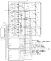
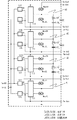
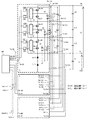
図1はこの発明の実施の形態1によるDC/DC電力変換装置の回路構成を示すものである。
図1に示すように、DC/DC電力変換装置は、それぞれ複数段(この場合4段)の回路A1〜A4から成る3つの列回路X、Y、Zと、駆動用電源Vs1、Vs2、Vs3、Vs4と、入出力電圧を平滑化し、またエネルギ移行のための電圧源としても機能する平滑コンデンサCs1、Cs2、Cs3、Cs4と、制御回路130と、入出力電圧端子Vcom、VL、VHとから構成される。そして、電圧端子VLとVcom間に入力された電圧V1を、約4倍に昇圧された電圧V2にして電圧端子VHとVcom間に出力する機能を有する。
A DC / DC power converter according to
FIG. 1 shows a circuit configuration of a DC / DC power conversion apparatus according to
As shown in FIG. 1, the DC / DC power converter includes three column circuits X, Y, and Z each including a plurality of stages (four stages in this case) of circuits A1 to A4, and driving power sources Vs1, Vs2, and Vs3. , Vs4, smoothing capacitors Cs1, Cs2, Cs3, Cs4 that smooth the input / output voltage and also function as a voltage source for energy transfer,
各列回路X、Y、Zは、それぞれ、電圧端子VLとVcom間に入力された電圧V1を、約4倍に昇圧された電圧V2にして電圧端子VHとVcom間に出力する機能を有するDC/DCコンバータで、各列回路の構成について以下に説明する。便宜上、列回路X内の回路構成のみ図示したが、列回路Y、Zの構成も同様である。
図1に示すように、列回路X(Y、Z)は、低圧側素子、高圧側素子としての2つのMOSFET(Mos1L、Mos1H)(Mos2L、Mos2H)(Mos3L、Mos3H)(Mos4L、Mos4H)を直列接続して、各平滑コンデンサCs1、Cs2、Cs3、Cs4の両端子間に接続した4段の回路A1、A2、A3、A4を直列接続して構成される。そして、各回路A1、A2、A3、A4内の2つのMOSFETの接続点を中間端子として、所定の1回路となる回路A1と他の各回路A2、A3、A4との中間端子間に、コンデンサCr12、Cr13、Cr14およびインダクタLr12、Lr13、Lr14の直列体で構成されエネルギ移行素子として機能するLC直列体LC12、LC13、LC14を接続する。各段のインダクタLrとコンデンサCrのインダクタンス値と容量値から定まる共振周期の値は、それぞれ等しくなるように設定されている。
なお、各MOSFETは、ソース、ドレイン間に寄生ダイオードが形成されているパワーMOSFETである。
Each column circuit X, Y, Z has a function of outputting the voltage V1 input between the voltage terminals VL and Vcom to the voltage V2 boosted about four times and outputting it between the voltage terminals VH and Vcom. A configuration of each column circuit in the / DC converter will be described below. For convenience, only the circuit configuration in the column circuit X is shown, but the configuration of the column circuits Y and Z is the same.
As shown in FIG. 1, the column circuit X (Y, Z) includes two MOSFETs (Mos1L, Mos1H) (Mos2L, Mos2H) (Mos3L, Mos3H) (Mos4L, Mos4H) as low-voltage side elements and high-voltage side elements. Four stages of circuits A1, A2, A3, A4 connected in series and connected between both terminals of each of the smoothing capacitors Cs1, Cs2, Cs3, Cs4 are connected in series. Then, with the connection point of the two MOSFETs in each circuit A1, A2, A3, A4 as an intermediate terminal, a capacitor is connected between the intermediate terminal of the circuit A1 that is a predetermined one circuit and each of the other circuits A2, A3, A4. LC series bodies LC12, LC13, and LC14 that are configured by a series body of Cr12, Cr13, and Cr14 and inductors Lr12, Lr13, and Lr14 and function as energy transfer elements are connected. The resonance period values determined from the inductance value and the capacitance value of the inductor Lr and the capacitor Cr at each stage are set to be equal to each other.
Each MOSFET is a power MOSFET in which a parasitic diode is formed between the source and drain.
また、列回路X(Y、Z)は、各回路A1〜A4内のMOSFETを駆動するための、ゲート駆動回路111〜114およびフォトカプラ(121L、121H)〜(124L、124H)を備える。さらに、ゲート信号入力端子Tm−GL、Tm−GHと、電源入力端子あるいは平滑コンデンサ接続端子となるTm−Com、Tm−Vs1〜Tm−Vs4、Tm−Cs1〜Tm−Cs4を備える。
各列回路X、Y、Zで共有する電源Vs1、Vs2、Vs3、Vs4は、それぞれMos1L、Mos2L、Mos3L、Mos4Lのソース端子を基準とした、各列回路X、Y、Z内のMOSFET、ゲート駆動回路111〜114およびフォトカプラ(121L、121H)〜(124L、124H)を駆動するために備えられた電源である。
The column circuit X (Y, Z) includes
The power sources Vs1, Vs2, Vs3, and Vs4 shared by the column circuits X, Y, and Z are MOSFETs and gates in the column circuits X, Y, and Z, respectively, based on the source terminals of Mos1L, Mos2L, Mos3L, and Mos4L. The power source is provided to drive the
次に、DC/DC電力変換装置内の接続の詳細について説明する。
平滑コンデンサCs1の低電圧側端子は、電圧端子Vcomと電源Vs1の負電圧端子と各列回路X、Y、Zの端子Tm−Comに接続される。平滑コンデンサCs1の高電圧側端子は、電圧端子VLと平滑コンデンサCs2の低電圧側端子と電源Vs2の負電圧端子と各列回路X、Y、Zの端子Tm−Cs1に接続される。平滑コンデンサCs2の高電圧側端子は、平滑コンデンサCs3の低電圧側端子と電源Vs3の負電圧端子と各列回路X、Y、Zの端子Tm−Cs2に接続される。平滑コンデンサCs3の高電圧側端子は、平滑コンデンサCs4の低電圧側端子と電源Vs4の負電圧端子と各列回路X、Y、Zの端子Tm−Cs3に接続される。平滑コンデンサCs4の高電圧側端子は、電圧端子VHと各列回路X、Y、Zの端子Tm−Cs4に接続される。各電源Vs1〜Vs4の正電圧端子は、各列回路X、Y、Zの端子Tm−Vs1〜Tm−Vs4に接続される。
Next, details of connection in the DC / DC power conversion apparatus will be described.
The low voltage side terminal of the smoothing capacitor Cs1 is connected to the voltage terminal Vcom, the negative voltage terminal of the power source Vs1, and the terminal Tm-Com of each column circuit X, Y, Z. The high voltage side terminal of the smoothing capacitor Cs1 is connected to the voltage terminal VL, the low voltage side terminal of the smoothing capacitor Cs2, the negative voltage terminal of the power source Vs2, and the terminals Tm-Cs1 of the column circuits X, Y, and Z. The high voltage side terminal of the smoothing capacitor Cs2 is connected to the low voltage side terminal of the smoothing capacitor Cs3, the negative voltage terminal of the power source Vs3, and the terminals Tm-Cs2 of the column circuits X, Y, and Z. The high voltage side terminal of the smoothing capacitor Cs3 is connected to the low voltage side terminal of the smoothing capacitor Cs4, the negative voltage terminal of the power source Vs4, and the terminals Tm-Cs3 of the column circuits X, Y, and Z. The high voltage side terminal of the smoothing capacitor Cs4 is connected to the voltage terminal VH and the terminal Tm-Cs4 of each column circuit X, Y, Z. The positive voltage terminals of the power sources Vs1 to Vs4 are connected to the terminals Tm-Vs1 to Tm-Vs4 of the column circuits X, Y, and Z.
各列回路内では以下のように接続される。
Mos1Lのソース端子は端子Tm−Comに、Mos1Hのドレイン端子とMos2Lのソース端子とは端子Tm−Cs1に接続され、Mos2Hのドレイン端子とMos3Lのソース端子とは端子Tm−Cs2に接続される。Mos3Hのドレイン端子とMos4Lのソース端子は端子Tm−Cs3に接続され、Mos4Hのドレイン端子は端子Tm−Cs4に接続される。
LC直列体LC12の一端は、Mos1LとMos1Hとの接続点に接続され、他端はMos2LとMos2Hとの接続点に接続される。LC直列体LC13の一端は、Mos1LとMos1Hとの接続点に接続され、他端はMos3LとMos3Hとの接続点に接続される。LC直列体LC14の一端は、Mos1LとMos1Hとの接続点に接続され、他端はMos4LとMos4Hとの接続点に接続されている。
In each column circuit, connections are made as follows.
The source terminal of Mos1L is connected to terminal Tm-Com, the drain terminal of Mos1H and the source terminal of Mos2L are connected to terminal Tm-Cs1, and the drain terminal of Mos2H and the source terminal of Mos3L are connected to terminal Tm-Cs2. The drain terminal of Mos3H and the source terminal of Mos4L are connected to terminal Tm-Cs3, and the drain terminal of Mos4H is connected to terminal Tm-Cs4.
One end of the LC series LC12 is connected to a connection point between Mos1L and Mos1H, and the other end is connected to a connection point between Mos2L and Mos2H. One end of the LC series LC13 is connected to a connection point between Mos1L and Mos1H, and the other end is connected to a connection point between Mos3L and Mos3H. One end of the LC series LC14 is connected to a connection point between Mos1L and Mos1H, and the other end is connected to a connection point between Mos4L and Mos4H.
またMos1L、Mos1Hのゲート端子はゲート駆動回路111の出力端子に接続され、ゲート駆動回路111の入力端子には、Mos1Lのソース端子の電圧を基準としたそれぞれのゲート駆動信号が入力される。同様に、(Mos2L、Mos2H)〜(Mos4L、Mos4H)のゲート端子はゲート駆動回路112〜114の出力端子に接続され、ゲート駆動回路112〜114の入力端子には、Mos2L〜Mos4Lのソース端子の電圧を基準としたそれぞれのゲート駆動信号が入力される。なお、ゲート駆動回路111〜114は、一般的なブートストラップ方式の駆動回路であり、ハーフブリッジインバータ回路駆動用のドライバICや高電圧側のMOSFETを駆動するためのコンデンサ等で構成されている。
The gate terminals of Mos1L and Mos1H are connected to the output terminal of the
Mos1L駆動用のゲート駆動信号はフォトカプラ121Lから、Mos1H駆動用のゲート駆動信号はフォトカプラ121Hから出力される。同様に、Mos2L〜Mos4L駆動用のゲート駆動信号はフォトカプラ122L〜124Lから、Mos2H〜Mos4H駆動用のゲート駆動信号はフォトカプラ122H〜124Hから出力される。フォトカプラ121L〜124L、121H〜124Hには、制御回路130から各列回路X、Y、Z毎に出力されるゲート信号GateL−X(GateL−Y、GateL−Z)、GateH−X(GateH−Y、GateH−Z)が入力される。
The gate drive signal for driving Mos1L is output from the photocoupler 121L, and the gate drive signal for driving Mos1H is output from the
次に各列回路X、Y、Zの動作について説明する。
回路A1は、電圧端子VL−Vcom間に入力されるエネルギを、MOSFET(Mos1L、Mos1H)のオンオフ動作により高電圧側に送る駆動用インバータ回路として動作する。また、回路A2、A3、A4は、駆動用インバータ回路A1で駆動された電流を整流し、エネルギを高電圧側へ移行する整流回路として動作する。制御回路130から各列回路X、Y、Z毎にゲート信号(GateL−X、GateH−X)、(GateL−Y、GateH−Y)、(GateL−Z、GateH−Z)が出力され、これらゲート信号により各列回路X、Y、Zが駆動される。
Next, the operation of each column circuit X, Y, Z will be described.
The circuit A1 operates as a drive inverter circuit that sends energy input between the voltage terminals VL and Vcom to the high voltage side by the on / off operation of the MOSFETs (Mos1L, Mos1H). The circuits A2, A3, and A4 operate as a rectifier circuit that rectifies the current driven by the driving inverter circuit A1 and transfers energy to the high voltage side. A gate signal (GateL-X, GateH-X), (GateL-Y, GateH-Y), (GateL-Z, GateH-Z) is output from the
平滑コンデンサCs1、Cs2、Cs3、Cs4の容量値は、LC直列体のコンデンサCr12、Cr13、Cr14の容量値と比較して十分大きな値に設定される。
上述したように、電圧端子VL−Vcom間に入力された電圧V1を、約4倍に昇圧された電圧V2にして電圧端子VH−Vcom間に出力するため、電圧端子VH−Vcom間に負荷が接続され、電圧V2は4×V1よりも低い値となっている。定常状態では、平滑コンデンサCs1には電圧V1の電圧が充電されており、平滑コンデンサCs2、Cs3、Cs4には平均的に(V2−V1)/3の電圧が充電されている。
The capacitance values of the smoothing capacitors Cs1, Cs2, Cs3, and Cs4 are set to a sufficiently large value as compared with the capacitance values of the LC series capacitors Cr12, Cr13, and Cr14.
As described above, since the voltage V1 input between the voltage terminals VL and Vcom is changed to the voltage V2 boosted by about 4 times and output between the voltage terminals VH and Vcom, a load is applied between the voltage terminals VH and Vcom. Connected, the voltage V2 is lower than 4 × V1. In the steady state, the smoothing capacitor Cs1 is charged with the voltage V1, and the smoothing capacitors Cs2, Cs3, and Cs4 are charged with an average voltage of (V2−V1) / 3.
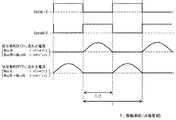
列回路Xのゲート信号(GateL−X、GateH−X)と、駆動用インバータ回路A1および整流回路A2〜A4内の高圧側MOSFET(Mos1H、Mos2H〜Mos4H)に流れる電流と低圧側MOSFET(Mos1L、Mos2L〜Mos4L)に流れる電流とを図2に示す。駆動用インバータ回路A1内のMOSFETではドレインからソースに電流が流れ、整流回路A2〜A4内のMOSFETではソースからドレインに電流が流れる。MOSFETはゲート信号がハイ電圧でオンする。
図2に示すように、ゲート信号(GateL−X、GateH−X)は、LrとCrによるLC直列体LC12、LC13、LC14にて定まる共振周期Tを周期とし、デューティー約50%のオンオフ信号である。なお、列回路Y、Zのゲート信号(GateL−Y、GateH−Y)、(GateL−Z、GateH−Z)および各列回路Y、Z内のMOSFETを流れる電流も、図2と同様である。
The gate signal (GateL-X, GateH-X) of the column circuit X, the current flowing through the high-voltage side MOSFETs (Mos1H, Mos2H-Mos4H) in the driving inverter circuit A1 and the rectifier circuits A2-A4, and the low-voltage side MOSFETs (Mos1L, FIG. 2 shows the current flowing through Mos2L to Mos4L). In the MOSFET in the driving inverter circuit A1, current flows from the drain to the source, and in the MOSFET in the rectifier circuits A2 to A4, current flows from the source to the drain. The MOSFET is turned on when the gate signal is high.
As shown in FIG. 2, the gate signals (GateL-X, GateH-X) are on / off signals with a resonance period T determined by the LC serial bodies LC12, LC13, LC14 of Lr and Cr, and a duty of about 50%. is there. The gate signals (GateL-Y, GateH-Y) and (GateL-Z, GateH-Z) of the column circuits Y and Z and the currents flowing through the MOSFETs in the column circuits Y and Z are the same as those in FIG. .
低圧側MOSFETへのゲート信号GateL(GateL−X、GateL−Y、GateL−Z)により各回路A1〜A4の低圧側MOSFETであるMos1L、Mos2L、Mos3L、Mos4Lがオン状態となると、電圧差があるため、平滑コンデンサCs1、Cs2、Cs3に蓄えられた一部のエネルギが、以下に示す経路でコンデンサCr12、Cr13、Cr14に移行する。
Cs1⇒Mos2L⇒Lr12⇒Cr12⇒Mos1L
Cs1⇒Cs2⇒Mos3L⇒Lr13⇒Cr13⇒Mos1L
Cs1⇒Cs2⇒Cs3⇒Mos4L⇒Lr14⇒Cr14⇒Mos1L
When the gate signals GateL (GateL-X, GateL-Y, GateL-Z) to the low-voltage side MOSFETs turn on the low-voltage side MOSFETs Mos1L, Mos2L, Mos3L, and Mos4L of the circuits A1 to A4, there is a voltage difference. Therefore, some energy stored in the smoothing capacitors Cs1, Cs2, and Cs3 is transferred to the capacitors Cr12, Cr13, and Cr14 through the following path.
Cs1⇒Mos2L⇒Lr12⇒Cr12⇒Mos1L
Cs1⇒Cs2⇒Mos3L⇒Lr13⇒Cr13⇒Mos1L
Cs1⇒Cs2⇒Cs3⇒Mos4L⇒Lr14⇒Cr14⇒Mos1L
次いで、高圧側MOSFETへのゲート信号GateH(GateH−X、GateH−Y、GateH−Z)により各回路A1〜A4の高圧側MOSFETであるMos1H、Mos2H、Mos3H、Mos4Hがオン状態となると、電圧差があるため、コンデンサCr12、Cr13、Cr14に充電されたエネルギが、以下に示す経路で平滑コンデンサCs2、Cs3、Cs4に移行する。
Cr12⇒Lr12⇒Mos2H⇒Cs2⇒Mos1H
Cr13⇒Lr13⇒Mos3H⇒Cs3⇒Cs2⇒Mos1H
Cr14⇒Lr14⇒Mos4H⇒Cs4⇒Cs3⇒Cs2⇒Mos1H
Next, when the gate signals GateH (GateH-X, GateH-Y, GateH-Z) to the high-voltage side MOSFETs turn on the high-voltage side MOSFETs Mos1H, Mos2H, Mos3H, Mos4H of the circuits A1 to A4, the voltage difference Therefore, the energy charged in the capacitors Cr12, Cr13, and Cr14 is transferred to the smoothing capacitors Cs2, Cs3, and Cs4 through the following path.
Cr12⇒Lr12⇒Mos2H⇒Cs2⇒Mos1H
Cr13⇒Lr13⇒Mos3H⇒Cs3⇒Cs2⇒Mos1H
Cr14⇒Lr14⇒Mos4H⇒Cs4⇒Cs3⇒Cs2⇒Mos1H
このように、コンデンサCr12、Cr13、Cr14の充放電により、平滑コンデンサCs1から平滑コンデンサCs2、Cs3、Cs4にエネルギを移行する。そして、電圧端子VLとVcom間に入力された電圧V1を、約4倍に昇圧された電圧V2にして電圧端子VHとVcom間に出力する。また、各コンデンサCr12、Cr13、Cr14には、インダクタLr12、Lr13、Lr14が直列に接続されてLC直列体LC12、LC13、LC14を構成するため、上記エネルギの移行は共振現象を利用したものとなり、大きなエネルギ量を効率よく移行できる。
またこの実施の形態では、整流回路A2〜A4にMOSFETを用いたため、ダイオードを用いたものに比して導通損失が低減でき、電力変換の効率が向上できる。
In this way, energy is transferred from the smoothing capacitor Cs1 to the smoothing capacitors Cs2, Cs3, and Cs4 by charging and discharging the capacitors Cr12, Cr13, and Cr14. Then, the voltage V1 input between the voltage terminals VL and Vcom is changed to a voltage V2 boosted about four times and output between the voltage terminals VH and Vcom. Also, inductors Lr12, Lr13, Lr14 are connected in series to each capacitor Cr12, Cr13, Cr14 to form an LC series body LC12, LC13, LC14, so the above energy transfer uses a resonance phenomenon, A large amount of energy can be transferred efficiently.
In this embodiment, since MOSFETs are used for the rectifier circuits A2 to A4, the conduction loss can be reduced as compared with the diodes, and the efficiency of power conversion can be improved.
また、この実施の形態では、平滑コンデンサCs1の両端子に入力端子となる低電圧側の電圧端子VL、Vcomが接続された駆動用インバータ回路A1と整流回路である他の各回路A2、A3、A4との間に、LC直列体LC12、LC13、LC14を接続した。
この実施の形態におけるLC直列体LC12、LC13、LC14に流れる電流値をI12、I13、I14とし、コンデンサCr12、Cr13、Cr14の電圧をV12、V13、V14とする。そして、比較例として、隣接する回路間、即ちA1、A2間、A2、A3間、A3、A4間で中間端子(低圧側MOSFETと高圧側MOSFETとの接続点)間に、LC直列体LC12、LC23、LC34を接続して、同様に動作させた場合を考える。この比較例におけるLC直列体LC12、LC23、LC34に流れる電流値をI12r、I23r、I34rとし、LC直列体LC12、LC23、LC34内のコンデンサCr12、Cr23、Cr34の電圧をV12r、V23r、V34rとすると、
In this embodiment, the drive inverter circuit A1 in which the low voltage side voltage terminals VL and Vcom serving as input terminals are connected to both terminals of the smoothing capacitor Cs1 and the other circuits A2, A3, which are rectifier circuits, LC serial bodies LC12, LC13, and LC14 were connected to A4.
In this embodiment, current values flowing through the LC series bodies LC12, LC13, and LC14 are I12, I13, and I14, and voltages of the capacitors Cr12, Cr13, and Cr14 are V12, V13, and V14. As a comparative example, an LC series body LC12, between adjacent circuits, that is, between A1, A2, A2, A3, A3, A4, between intermediate terminals (connection point between the low voltage side MOSFET and the high voltage side MOSFET), Consider a case where LC23 and LC34 are connected and operated in the same manner. In this comparative example, the current values flowing through the LC series bodies LC12, LC23, LC34 are I12r, I23r, I34r, and the voltages of the capacitors Cr12, Cr23, Cr34 in the LC series bodies LC12, LC23, LC34 are V12r, V23r, V34r. ,
比較例において
I12r:I23r:I34r=3:2:1
V12r=V23r=V34r
であるのに対し、この実施の形態では、
I12=I13=I14(=I34r)
V12:V13:V14=1:2:3 (V12=V12r=V23r=V34r)
となる。
このように、この実施の形態では、回路A1と他の各回路A2、A3、A4との中間端子間にLC直列体LC12、LC13、LC14を接続したため、上記比較例に比べて、コンデンサCr12、Cr13、Cr14の電圧は増大するものであるが、LC直列体LC12を流れる電流値を1/3に、また高圧側が回路A3に接続されるLC直列体LC13では、比較例のLC直列体LC23を流れる電流値の1/2に低減できる。即ち、各LC直列体LC12、LC13、LC14を流れる電流値を最小のものと等しくできる。このため、エネルギ移行用のLC直列体LC12、LC13、LC14のインダクタLr、コンデンサCrの電流定格を低下させ、インダクタLrとコンデンサCrを小形化することができる。
In the comparative example
I12r: I23r: I34r = 3: 2: 1
V12r = V23r = V34r
In contrast, in this embodiment,
I12 = I13 = I14 (= I34r)
V12: V13: V14 = 1: 2: 3 (V12 = V12r = V23r = V34r)
It becomes.
Thus, in this embodiment, since the LC series bodies LC12, LC13, LC14 are connected between the intermediate terminals of the circuit A1 and the other circuits A2, A3, A4, compared to the comparative example, the capacitors Cr12, Although the voltages of Cr13 and Cr14 increase, the current value flowing through the LC series body LC12 is reduced to 1/3, and the LC series body LC13 whose high voltage side is connected to the circuit A3 has the LC series body LC23 of the comparative example. The current value can be reduced to 1/2. That is, the current value flowing through each LC series LC12, LC13, LC14 can be made equal to the minimum value. For this reason, the current ratings of the inductor Lr and the capacitor Cr of the LC series bodies LC12, LC13, and LC14 for energy transfer can be reduced, and the inductor Lr and the capacitor Cr can be reduced in size.
以上のように各列回路X、Y、Zは動作するものであるが、3つの列回路X、Y、Zを備えたDC/DC電力変換装置全体の動作について、以下に説明する。
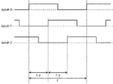
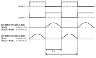
図3に、各列回路X、Y、Z内の高圧側MOSFETを駆動するゲート信号GateH−X、GateH−Y、GateH−Zを示す。図2を用いて示したように、このゲート信号GateH−X、GateH−Y、GateH−Zの反転信号が、低圧側MOSFETを駆動するGateL−X、GateL−Y、GateL−Zである。
図3に示すように、各列回路X、Y、Zを駆動する駆動信号は、周期をTとして一致させると共に、各列回路間で位相をT/3ずつずらして駆動している。
As described above, the column circuits X, Y, and Z operate. The operation of the entire DC / DC power conversion apparatus including the three column circuits X, Y, and Z will be described below.
FIG. 3 shows gate signals GateH-X, GateH-Y, and GateH-Z for driving the high-voltage side MOSFETs in the column circuits X, Y, and Z. As shown in FIG. 2, the inverted signals of the gate signals GateH-X, GateH-Y, and GateH-Z are GateL-X, GateL-Y, and GateL-Z that drive the low-voltage side MOSFET.
As shown in FIG. 3, the drive signals for driving the column circuits X, Y, and Z are driven with a period of T and the phase of each column circuit being shifted by T / 3.
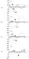
例えば、V1の電圧36V、入力直流電流280Aの条件における、平滑コンデンサCs1、Cs2、Cs3、Cs4に流れる電流を図4に示す。図には、3つの列回路で位相をT/3ずつずらして駆動した場合(図中、3重)、即ちこの実施の形態の場合の平滑コンデンサ電流と、比較例として列回路1つで駆動した場合(図中、1重)、列回路2つで位相をT/2ずらして駆動した場合(図中、2重)の平滑コンデンサ電流を示した。縦軸は電流、横軸は時間である。
図4に示すように、3つの列回路で位相をT/3ずつずらして駆動した場合、列回路が1つ、あるいは2つの場合より平滑コンデンサCs1、Cs2、Cs3、Cs4のリプル電流が減少する。また、列回路の数を増加するほど平滑コンデンサCs1、Cs2、Cs3、Cs4のリプル電流が低減する。
For example, FIG. 4 shows currents flowing through the smoothing capacitors Cs1, Cs2, Cs3, and Cs4 under the conditions of a voltage V1 of 36V and an input DC current 280A. In the figure, when driving by shifting the phase by T / 3 by three column circuits (triple in the figure), that is, smoothing capacitor current in this embodiment, driving by one column circuit as a comparative example In this case (single in the figure), the smoothing capacitor current is shown when the phase is shifted by T / 2 with two column circuits (double in the figure). The vertical axis is current, and the horizontal axis is time.
As shown in FIG. 4, when the three column circuits are driven by shifting the phase by T / 3, the ripple current of the smoothing capacitors Cs1, Cs2, Cs3, and Cs4 is reduced as compared with the case of one or two column circuits. . Further, the ripple current of the smoothing capacitors Cs1, Cs2, Cs3, and Cs4 decreases as the number of column circuits increases.
以上のように、この実施の形態では、それぞれ4段の回路A1、A2、A3、A4から成る3つの列回路X、Y、Zを、列回路内の各回路A1、A2、A3、A4に並列配置される平滑コンデンサCs1、Cs2、Cs3、Cs4を共有して並列接続し、各列回路X、Y、Zを、駆動周期を一致させると共に各列回路毎に位相を2π/3(rad)ずらして駆動した。これにより、平滑コンデンサCs1、Cs2、Cs3、Cs4の充放電タイミングがずれ、平滑コンデンサCs1、Cs2、Cs3、Cs4への充放電電流を列回路間で融通し合うため、平滑コンデンサCs1、Cs2、Cs3、Cs4に流れる交流電流(リプル電流)が低減する。
なお、3つの列回路が、仮に平滑コンデンサCs1、Cs2、Cs3、Cs4を共有せずに、各列回路がそれぞれ平滑コンデンサCs1、Cs2、Cs3、Cs4を備えて並列接続したとすれば、各列回路を上記実施の形態1と同様に動作させたとしても、それぞれ3個ずつある平滑コンデンサCs1、Cs2、Cs3、Cs4は電流の共有化が図れずにリプル電流は低減できないものである。
As described above, in this embodiment, three column circuits X, Y, and Z each including four stages of circuits A1, A2, A3, and A4 are replaced with the respective circuits A1, A2, A3, and A4 in the column circuit. The smoothing capacitors Cs1, Cs2, Cs3, and Cs4 that are arranged in parallel are shared and connected in parallel, and the column circuits X, Y, and Z are matched in drive cycle and the phase of each column circuit is 2π / 3 (rad). Driven by shifting. As a result, the charging / discharging timing of the smoothing capacitors Cs1, Cs2, Cs3, Cs4 is shifted, and the charging / discharging currents to the smoothing capacitors Cs1, Cs2, Cs3, Cs4 are interchanged between the column circuits, so that the smoothing capacitors Cs1, Cs2, Cs3 , AC current (ripple current) flowing through Cs4 is reduced.
Assuming that the three column circuits do not share the smoothing capacitors Cs1, Cs2, Cs3, and Cs4, but each column circuit includes the smoothing capacitors Cs1, Cs2, Cs3, and Cs4 and is connected in parallel. Even if the circuit is operated in the same manner as in the first embodiment, the three smoothing capacitors Cs1, Cs2, Cs3, and Cs4 can not reduce the ripple current without sharing the current.
このような平滑コンデンサのリプル電流低減により、以下のような効果がある。
平滑コンデンサの発熱が抑制され信頼性が向上する。また、電流低減により抵抗分による損失が低減し電力変換効率が向上する。また、平滑コンデンサに必要な容量を低下でき平滑コンデンサのサイズを小さくでき、装置構成の小型化を促進できる。
さらにまた、誘電損失は大きいがサイズが小さいセラミックコンデンサを平滑コンデンサに採用することが可能になり、平滑コンデンサのサイズをさらに小さくできる。
Such reduction of the ripple current of the smoothing capacitor has the following effects.
Heat generation of the smoothing capacitor is suppressed and reliability is improved. Further, the loss due to resistance is reduced by reducing the current, and the power conversion efficiency is improved. Further, the capacity required for the smoothing capacitor can be reduced, the size of the smoothing capacitor can be reduced, and the downsizing of the device configuration can be promoted.
Furthermore, a ceramic capacitor having a large dielectric loss but a small size can be adopted as the smoothing capacitor, and the size of the smoothing capacitor can be further reduced.
なお、上記実施の形態では、列回路を3個としたが、複数(n個)配列し位相を各列回路間で2π/n(rad)ずつずらして駆動することにより、平滑コンデンサCs1、Cs2、Cs3、Cs4のリプル電流が減少する効果が得られる。また、列回路の数nを増加するほど平滑コンデンサCs1、Cs2、Cs3、Cs4のリプル電流が低減できる。
また、各列回路間で2π/n(rad)ずつ位相をずらして駆動するのが最も効果的であるが、位相差は、これに限らず、各列回路間で位相をずらすことにより、平滑コンデンサCs1、Cs2、Cs3、Cs4への充放電電流を列回路間で融通し合えるため、リプル電流低減の効果がある。
In the above embodiment, the number of column circuits is three. However, smoothing capacitors Cs1, Cs2 can be obtained by arranging a plurality (n) of column circuits and shifting the phase by 2π / n (rad) between the column circuits. , Cs3, Cs4 ripple current can be reduced. Further, the ripple current of the smoothing capacitors Cs1, Cs2, Cs3, and Cs4 can be reduced as the number of column circuits n is increased.
In addition, it is most effective to drive each column circuit by shifting the phase by 2π / n (rad). However, the phase difference is not limited to this, and smoothing is possible by shifting the phase between each column circuit. Since the charge / discharge currents to the capacitors Cs1, Cs2, Cs3, and Cs4 can be interchanged between the column circuits, the ripple current can be reduced.
実施の形態2.
上記実施の形態1では、電圧V1を、約4倍の電圧V2に昇圧する昇圧形のDC/DC電力変換装置について示したが、この実施の形態では、電圧V2から電圧V1に降圧する降圧形のDC/DC電力変換装置について示す。
この実施の形態によるDC/DC電力変換装置の回路構成は、図1で示す回路構成と同様であるが、この場合、各列回路X、Y、Z内の回路A2、A3、A4は駆動用インバータ回路として動作し、回路A1は、駆動用インバータ回路で駆動された電流を整流し、エネルギを低電圧側へ移行する整流回路として動作する。制御回路130から各列回路X、Y、Z毎にゲート信号(GateL−X、GateH−X)、(GateL−Y、GateH−Y)、(GateL−Z、GateH−Z)が出力され、これらゲート信号により各列回路X、Y、Zが駆動される。
In the first embodiment, the step-up DC / DC power converter that boosts the voltage V1 to about four times the voltage V2 has been described. However, in this embodiment, the step-down type steps down the voltage V2 to the voltage V1. A DC / DC power conversion apparatus will be described.
The circuit configuration of the DC / DC power converter according to this embodiment is the same as the circuit configuration shown in FIG. 1, but in this case, the circuits A2, A3, A4 in each column circuit X, Y, Z are for driving. The circuit A1 operates as an inverter circuit, and operates as a rectifier circuit that rectifies the current driven by the driving inverter circuit and shifts energy to the low voltage side. A gate signal (GateL-X, GateH-X), (GateL-Y, GateH-Y), (GateL-Z, GateH-Z) is output from the
各列回路X、Y、Zの動作について以下に説明する。
平滑コンデンサCs1、Cs2、Cs3、Cs4の容量値は、LC直列体のコンデンサCr12、Cr13、Cr14の容量値と比較して十分大きな値に設定される。各列回路X、Y、Zは、それぞれ電圧端子VH−Vcom間に入力された電圧V2を、約1/4倍に降圧された電圧V1にして電圧端子VL−Vcom間に出力する機能を有するDC/DCコンバータであるため、電圧端子VL−Vcom間に負荷が接続され、電圧V2は4×V1よりも高い値となっている。定常状態では、平滑コンデンサCs1には電圧V1の電圧が充電されており、平滑コンデンサCs2、Cs3、Cs4には平均的に(V2−V1)/3の電圧が充電されている。
The operation of each column circuit X, Y, Z will be described below.
The capacitance values of the smoothing capacitors Cs1, Cs2, Cs3, and Cs4 are set to a sufficiently large value as compared with the capacitance values of the LC series capacitors Cr12, Cr13, and Cr14. Each of the column circuits X, Y, and Z has a function of converting the voltage V2 input between the voltage terminals VH and Vcom into a voltage V1 stepped down by about 1/4 and outputting the voltage V1 between the voltage terminals VL and Vcom. Since it is a DC / DC converter, a load is connected between the voltage terminals VL and Vcom, and the voltage V2 is higher than 4 × V1. In the steady state, the smoothing capacitor Cs1 is charged with the voltage V1, and the smoothing capacitors Cs2, Cs3, and Cs4 are charged with an average voltage of (V2−V1) / 3.
列回路Xのゲート信号(GateL−X、GateH−X)と、駆動用インバータ回路A2〜A4および整流回路A1内の高圧側MOSFET(Mos2H〜Mos4H、Mos1H)に流れる電流と低圧側MOSFET(Mos2L〜Mos4L、Mos1L)に流れる電流とを図5に示す。駆動用インバータ回路A2〜A4内のMOSFETではドレインからソースに電流が流れ、整流回路A1内のMOSFETではソースからドレインに電流が流れる。MOSFETはゲート信号がハイ電圧でオンする。
図5に示すように、ゲート信号(GateL−X、GateH−X)は、LrとCrによるLC直列体LC12、LC13、LC14にて定まる共振周期Tを周期とし、デューティー約50%のオンオフ信号である。なお、列回路Y、Zのゲート信号(GateL−Y、GateH−Y)、(GateL−Z、GateH−Z)および各列回路Y、Z内のMOSFETを流れる電流も、図5と同様である。
The gate signal (GateL-X, GateH-X) of the column circuit X, the current flowing through the high-voltage side MOSFETs (Mos2H to Mos4H, Mos1H) in the driving inverter circuits A2 to A4 and the rectifier circuit A1, and the low-voltage side MOSFETs (Mos2L to FIG. 5 shows the current flowing through Mos4L and Mos1L). In the MOSFETs in the drive inverter circuits A2 to A4, current flows from the drain to the source, and in the MOSFET in the rectifier circuit A1, current flows from the source to the drain. The MOSFET is turned on when the gate signal is high.
As shown in FIG. 5, the gate signals (GateL-X, GateH-X) are on / off signals with a duty cycle of about 50%, with a resonance period T determined by the LC series LC12, LC13, LC14 of Lr and Cr. is there. The gate signals (GateL-Y, GateH-Y) and (GateL-Z, GateH-Z) of the column circuits Y and Z and the currents flowing through the MOSFETs in the column circuits Y and Z are the same as in FIG. .
高圧側MOSFETへのゲート信号GateH(GateH−X、GateH−Y、GateH−Z)により各回路A2〜A4、A1の高圧側MOSFETであるMos2H、Mos3H、Mos4H、Mos1Hがオン状態となると、電圧差があるため、平滑コンデンサCs2、Cs3、Cs4に蓄えられた一部のエネルギが、以下に示す経路でコンデンサCr12、Cr13、Cr14に移行する。
Cs2⇒Cs3⇒Cs4⇒Mos4H⇒Lr14⇒Cr14⇒Mos1H
Cs2⇒Cs3⇒Mos3H⇒Lr13⇒Cr13⇒Mos1H
Cs2⇒Mos2H⇒Lr12⇒Cr12⇒Mos1H
When the gate signals GateH (GateH-X, GateH-Y, GateH-Z) to the high-voltage side MOSFET turn on the high-voltage side MOSFETs Mos2H, Mos3H, Mos4H, Mos1H of each circuit A2 to A4, A1, the voltage difference Therefore, some energy stored in the smoothing capacitors Cs2, Cs3, and Cs4 is transferred to the capacitors Cr12, Cr13, and Cr14 through the following path.
Cs2⇒Cs3⇒Cs4⇒Mos4H⇒Lr14⇒Cr14⇒Mos1H
Cs2⇒Cs3⇒Mos3H⇒Lr13⇒Cr13⇒Mos1H
Cs2⇒Mos2H⇒Lr12⇒Cr12⇒Mos1H
次いで、低圧側MOSFETへのゲート信号GateL(GateL−X、GateL−Y、GateL−Z)により各回路A2〜A4、A1の低圧側MOSFETであるMos2L、Mos3L、Mos4L、Mos1Lがオン状態となると、電圧差があるため、コンデンサCr12、Cr13、Cr14に充電されたエネルギが、以下に示す経路で平滑コンデンサCs1、Cs2、Cs3に移行する。
Cr14⇒Lr14⇒Mos4L⇒Cs3⇒Cs2⇒Cs1⇒Mos1L
Cr13⇒Lr13⇒Mos3L⇒Cs2⇒Cs1⇒Mos1L
Cr12⇒Lr12⇒Mos2L⇒Cs1⇒Mos1L
Next, when the gate signals GateL (GateL-X, GateL-Y, GateL-Z) to the low-voltage side MOSFETs, Mos2L, Mos3L, Mos4L, and Mos1L, which are the low-voltage side MOSFETs of the circuits A2 to A4 and A1, are turned on. Since there is a voltage difference, the energy charged in the capacitors Cr12, Cr13, Cr14 is transferred to the smoothing capacitors Cs1, Cs2, Cs3 through the following path.
Cr14⇒Lr14⇒Mos4L⇒Cs3⇒Cs2⇒Cs1⇒Mos1L
Cr13⇒Lr13⇒Mos3L⇒Cs2⇒Cs1⇒Mos1L
Cr12⇒Lr12⇒Mos2L⇒Cs1⇒Mos1L
このように、コンデンサCr12、Cr13、Cr14の充放電により、平滑コンデンサCs2、Cs3、Cs4から平滑コンデンサCs1にエネルギを移行する。そして、電圧端子VHとVcom間に入力された電圧V2を、約1/4倍に降圧された電圧V1にして電圧端子VLとVcom間に出力する。また、各コンデンサCr12、Cr13、Cr14には、インダクタLr12、Lr13、Lr14が直列に接続されてLC直列体LC12、LC13、LC14を構成するため、上記エネルギの移行は共振現象を利用したものとなり、大きなエネルギ量を効率よく移行できる。
またこの実施の形態では、整流回路A1にMOSFETを用いたため、ダイオードを用いたものに比して導通損失が低減でき、電力変換の効率が向上できる。
As described above, energy is transferred from the smoothing capacitors Cs2, Cs3, and Cs4 to the smoothing capacitor Cs1 by charging and discharging the capacitors Cr12, Cr13, and Cr14. Then, the voltage V2 input between the voltage terminals VH and Vcom is converted to a voltage V1 that has been stepped down by about 1/4 and output between the voltage terminals VL and Vcom. Also, inductors Lr12, Lr13, Lr14 are connected in series to each capacitor Cr12, Cr13, Cr14 to form an LC series body LC12, LC13, LC14, so the above energy transfer uses a resonance phenomenon, A large amount of energy can be transferred efficiently.
In this embodiment, since the MOSFET is used for the rectifier circuit A1, the conduction loss can be reduced and the efficiency of power conversion can be improved as compared with the case where the diode is used.
また、この実施の形態では、平滑コンデンサCs1の両端子に入力端子となる低電圧側の電圧端子VL、Vcomが接続された整流回路A1と駆動用インバータ回路である他の各回路A2、A3、A4との間に、LC直列体LC12、LC13、LC14を接続した。そして、この実施の形態においても、上記実施の形態1で示した比較例、即ち、隣接する回路間に、LC直列体LC12、LC23、LC34を接続して、同様に動作させた場合と比較して、LC直列体LC12を流れる電流値を1/3に、また高圧側が回路A3に接続されるLC直列体LC13では、比較例のLC直列体LC23を流れる電流値の1/2に低減できる。即ち、各LC直列体LC12、LC13、LC14を流れる電流値を最小のものと等しくできる。このため、エネルギ移行用のLC直列体LC12、LC13、LC14のインダクタLr、コンデンサCrの電流定格を低下させ、インダクタLrとコンデンサCrを小形化することができる。 In this embodiment, the rectifier circuit A1 in which the low-voltage side voltage terminals VL and Vcom serving as input terminals are connected to both terminals of the smoothing capacitor Cs1, and the other circuits A2, A3, which are drive inverter circuits, LC serial bodies LC12, LC13, and LC14 were connected to A4. This embodiment is also compared with the comparative example shown in the first embodiment, that is, when the LC series bodies LC12, LC23, and LC34 are connected between adjacent circuits and operated in the same manner. Thus, the current value flowing through the LC series body LC12 can be reduced to LC, and the LC series body LC13 whose high-voltage side is connected to the circuit A3 can be reduced to ½ of the current value flowing through the LC series body LC23 of the comparative example. That is, the current value flowing through each LC series LC12, LC13, LC14 can be made equal to the minimum value. For this reason, the current ratings of the inductor Lr and the capacitor Cr of the LC series bodies LC12, LC13, and LC14 for energy transfer can be reduced, and the inductor Lr and the capacitor Cr can be reduced in size.
以上のように各列回路X、Y、Zは動作するものであるが、各列回路X、Y、Zを駆動する駆動信号は、上記実施の形態1と同様に、周期をT(LC直列体にて定まる共振周期)として一致させると共に、各列回路間で位相をT/3(2π/3(rad))ずつずらして駆動する(図3参照)。また、3つの列回路X、Y、Zは、列回路内の各回路A1、A2、A3、A4に並列配置される平滑コンデンサCs1、Cs2、Cs3、Cs4を共有して並列接続される。これにより、平滑コンデンサCs1、Cs2、Cs3、Cs4の充放電タイミングがずれ、平滑コンデンサCs1、Cs2、Cs3、Cs4への充放電電流を列回路間で融通し合うため、平滑コンデンサCs1、Cs2、Cs3、Cs4に流れる交流電流(リプル電流)が低減する。このような平滑コンデンサのリプル電流低減により、上記実施の形態1と同様に、信頼性の向上、電力変換効率の向上、および装置構成の小型化が図れる。 As described above, each column circuit X, Y, Z operates, but the drive signal for driving each column circuit X, Y, Z has a cycle of T (LC series) as in the first embodiment. (Resonance period determined by the body) and the phase is shifted by T / 3 (2π / 3 (rad)) between the column circuits (see FIG. 3). The three column circuits X, Y, and Z are connected in parallel by sharing smoothing capacitors Cs1, Cs2, Cs3, and Cs4 arranged in parallel with the circuits A1, A2, A3, and A4 in the column circuit. As a result, the charging / discharging timing of the smoothing capacitors Cs1, Cs2, Cs3, Cs4 is shifted, and the charging / discharging currents to the smoothing capacitors Cs1, Cs2, Cs3, Cs4 are interchanged between the column circuits, so that the smoothing capacitors Cs1, Cs2, Cs3 , AC current (ripple current) flowing through Cs4 is reduced. By reducing the ripple current of such a smoothing capacitor, as in the first embodiment, it is possible to improve reliability, improve power conversion efficiency, and reduce the size of the device configuration.
なお、この実施の形態においても、列回路の個数および位相差は上述したものに限らず、列回路を複数(n個)配列して位相を各列回路間でずらして駆動することにより、平滑コンデンサCs1、Cs2、Cs3、Cs4のリプル電流が減少する効果が得られる。また、各列回路の位相を2π/n(rad)ずつずらすのが最も効果的であり、さらに、列回路の数nを増加するほど平滑コンデンサCs1、Cs2、Cs3、Cs4のリプル電流が低減できる。 In this embodiment, the number of column circuits and the phase difference are not limited to those described above, and a plurality of (n) column circuits are arranged and driven by shifting the phase between the column circuits. An effect of reducing the ripple current of the capacitors Cs1, Cs2, Cs3, and Cs4 can be obtained. Further, it is most effective to shift the phase of each column circuit by 2π / n (rad), and the ripple current of the smoothing capacitors Cs1, Cs2, Cs3, and Cs4 can be reduced as the number n of column circuits is increased. .
また、上記実施の形態1ではV1⇒V2の昇圧形DC/DC電力変換装置について示し、上記実施の形態2ではV2⇒V1の降圧形DC/DC電力変換装置について示したが、上記実施の形態1、2の機能を併せ持って双方向のエネルギ移行を実現することもできる。この場合、V1×4>V2のとき昇圧動作を行い、昇圧時には回路A1を駆動用インバータ回路に、回路A2、A3、A4を整流回路に用いる。また、V1×4<V2のときに降圧動作を行い、降圧時には回路A2、A3、A4を駆動用インバータ回路に、回路A1を整流回路に用いる。
このように制御される昇降圧形のDC/DC電力変換装置では、上記実施の形態1、2と同様の効果が得られると共に、1つの回路で双方向のエネルギ移行を実現でき広く利用できる。
In the first embodiment, the step-up DC / DC power converter of V1⇒V2 is shown. In the second embodiment, the step-down DC / DC power converter of V2 → V1 is shown. Bidirectional energy transfer can also be realized by combining the functions of 1 and 2. In this case, a boosting operation is performed when V1 × 4> V2, and the circuit A1 is used as a drive inverter circuit and the circuits A2, A3, and A4 are used as a rectifier circuit when boosting. Further, when V1 × 4 <V2, the step-down operation is performed, and at the time of step-down, the circuits A2, A3, A4 are used as a drive inverter circuit, and the circuit A1 is used as a rectifier circuit.
The step-up / step-down DC / DC power converter controlled in this way can achieve the same effects as those of the first and second embodiments, and can be widely used because a single circuit can realize bidirectional energy transfer.
実施の形態3.
次に、この発明の実施の形態3によるDC/DC電力変換装置について説明する。
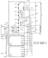
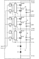
この実施の形態によるDC/DC電力変換装置の回路構成は、図1で示す回路構成において、各列回路X、Y、Zの構成が異なるもので、各列回路X、Y、Zの回路構成を図6に示す。その他の構成は図1と同様である。
上記実施の形態1と同様に、各列回路X、Y、Zは、それぞれ、電圧端子VLとVcom間に入力された電圧V1を、約4倍に昇圧された電圧V2にして電圧端子VHとVcom間に出力する機能を有するDC/DCコンバータである。
Next, a DC / DC power converter according to
The circuit configuration of the DC / DC power converter according to this embodiment is different from the circuit configuration shown in FIG. 1 in the configuration of each column circuit X, Y, Z. The circuit configuration of each column circuit X, Y, Z Is shown in FIG. Other configurations are the same as those in FIG.
As in the first embodiment, each of the column circuits X, Y, and Z converts the voltage V1 input between the voltage terminals VL and Vcom to the voltage V2 boosted about four times and the voltage terminal VH. This is a DC / DC converter with a function to output between Vcom.
図6に示すように、列回路X(Y、Z)は、低圧側素子、高圧側素子としての2つのMOSFET(Mos1L、Mos1H)(Mos2L、Mos2H)(Mos3L、Mos3H)(Mos4L、Mos4H)を直列接続して、各平滑コンデンサCs1、Cs2、Cs3、Cs4の両端子間に接続した4段の回路A1、A2、A3、A4を直列接続して構成される(図1参照)。そして、各回路A1、A2、A3、A4内の2つのMOSFETの接続点を中間端子として、隣接する各回路、即ち(A1,A2)(A2,A3)(A3,A4)の中間端子間に、コンデンサCr12、Cr23、Cr34およびインダクタLr12、Lr23、Lr34の直列体で構成されエネルギ移行素子として機能するLC直列体LC12、LC23、LC34を接続する。各段のインダクタLrとコンデンサCrのインダクタンス値と容量値から定まる共振周期の値は、それぞれ等しくなるように設定されている。
なお、各MOSFETは、ソース、ドレイン間に寄生ダイオードが形成されているパワーMOSFETである。
As shown in FIG. 6, the column circuit X (Y, Z) includes two MOSFETs (Mos1L, Mos1H) (Mos2L, Mos2H) (Mos3L, Mos3H) (Mos4L, Mos4H) as low-voltage side elements and high-voltage side elements. Four stages of circuits A1, A2, A3, A4 connected in series and connected between both terminals of each of the smoothing capacitors Cs1, Cs2, Cs3, Cs4 are connected in series (see FIG. 1). Then, using the connection point of the two MOSFETs in each circuit A1, A2, A3, A4 as an intermediate terminal, between adjacent circuits, that is, between the intermediate terminals of (A1, A2) (A2, A3) (A3, A4) LC series bodies LC12, LC23, and LC34 that are constituted by series bodies of capacitors Cr12, Cr23, and Cr34 and inductors Lr12, Lr23, and Lr34 and that function as energy transfer elements are connected. The resonance period values determined from the inductance value and the capacitance value of the inductor Lr and the capacitor Cr at each stage are set to be equal to each other.
Each MOSFET is a power MOSFET in which a parasitic diode is formed between the source and drain.
また、列回路X(Y、Z)は、各回路A1〜A4内のMOSFETを駆動するための、ゲート駆動回路111〜114およびフォトカプラ(121L、121H)〜(124L、124H)を備える。さらに、ゲート信号入力端子Tm−GL、Tm−GHと、電源入力端子あるいは平滑コンデンサ接続端子となるTm−Com、Tm−Vs1〜Tm−Vs4、Tm−Cs1〜Tm−Cs4を備える。
The column circuit X (Y, Z) includes
この実施の形態では、LC直列体LC12の一端は、Mos1LとMos1Hとの接続点に接続され、他端はMos2LとMos2Hとの接続点に接続される。LC直列体LC23の一端は、Mos2LとMos2Hの接続点に接続され、他端はMos3LとMos3Hの接続点に接続される。LC直列体LC34の一端は、Mos3LとMos3Hの接続点に接続され、他端はMos4LとMos4Hの接続点に接続される。その他の接続構成は上記実施の形態1と同様である。 In this embodiment, one end of the LC series body LC12 is connected to a connection point between Mos1L and Mos1H, and the other end is connected to a connection point between Mos2L and Mos2H. One end of the LC series LC23 is connected to a connection point between Mos2L and Mos2H, and the other end is connected to a connection point between Mos3L and Mos3H. One end of the LC series LC34 is connected to a connection point between Mos3L and Mos3H, and the other end is connected to a connection point between Mos4L and Mos4H. Other connection configurations are the same as those in the first embodiment.
次に各列回路X、Y、Zの動作について説明する。
上記実施の形態1と同様に、回路A1は駆動用インバータ回路として動作し、回路A2、A3、A4は、駆動用インバータ回路A1で駆動された電流を整流し、エネルギを高電圧側へ移行する整流回路として動作する。制御回路130から各列回路X、Y、Z毎にゲート信号(GateL−X、GateH−X)、(GateL−Y、GateH−Y)、(GateL−Z、GateH−Z)が出力され、これらゲート信号により各列回路X、Y、Zが駆動される。このゲート信号も、上記実施の形態1と同様であり、各回路A1〜A4内のMOSFETに流れる電流とゲート信号との関係も上記実施の形態1の図2で示したものと同様である。
Next, the operation of each column circuit X, Y, Z will be described.
As in the first embodiment, the circuit A1 operates as a drive inverter circuit, and the circuits A2, A3, and A4 rectify the current driven by the drive inverter circuit A1 and shift the energy to the high voltage side. Operates as a rectifier circuit. A gate signal (GateL-X, GateH-X), (GateL-Y, GateH-Y), (GateL-Z, GateH-Z) is output from the
平滑コンデンサCs1、Cs2、Cs3、Cs4の容量値は、LC直列体のコンデンサCr12、Cr13、Cr14の容量値と比較して十分大きな値に設定される。電圧端子VH−Vcom間に負荷が接続され、電圧V2は4×V1よりも低い値となっている。定常状態では、平滑コンデンサCs1には電圧V1の電圧が充電されており、平滑コンデンサCs2、Cs3、Cs4には平均的に(V2−V1)/3の電圧が充電されている。 The capacitance values of the smoothing capacitors Cs1, Cs2, Cs3, and Cs4 are set to a sufficiently large value as compared with the capacitance values of the LC series capacitors Cr12, Cr13, and Cr14. A load is connected between the voltage terminals VH and Vcom, and the voltage V2 is lower than 4 × V1. In the steady state, the smoothing capacitor Cs1 is charged with the voltage V1, and the smoothing capacitors Cs2, Cs3, and Cs4 are charged with an average voltage of (V2−V1) / 3.
低圧側MOSFETへのゲート信号GateL(GateL−X、GateL−Y、GateL−Z)により各回路A1〜A4の低圧側MOSFETであるMos1L、Mos2L、Mos3L、Mos4Lがオン状態となると、電圧差があるため、平滑コンデンサCs1、Cs2、Cs3に蓄えられた一部のエネルギが、以下に示す経路でコンデンサCr12、Cr23、Cr34に移行する。
Cs1⇒Mos2L⇒Lr12⇒Cr12⇒Mos1L
Cs1⇒Cs2⇒Mos3L⇒Lr23⇒Cr23⇒Lr12⇒Cr12⇒Mos1L
Cs1⇒Cs2⇒Cs3⇒Mos4L⇒Lr34⇒Cr34⇒Lr23⇒Cr23⇒Lr12⇒Cr12⇒Mos1L
When the gate signals GateL (GateL-X, GateL-Y, GateL-Z) to the low-voltage side MOSFETs turn on the low-voltage side MOSFETs Mos1L, Mos2L, Mos3L, and Mos4L of the circuits A1 to A4, there is a voltage difference. Therefore, a part of energy stored in the smoothing capacitors Cs1, Cs2, and Cs3 is transferred to the capacitors Cr12, Cr23, and Cr34 through the following path.
Cs1⇒Mos2L⇒Lr12⇒Cr12⇒Mos1L
Cs1⇒Cs2⇒Mos3L⇒Lr23⇒Cr23⇒Lr12⇒Cr12⇒Mos1L
Cs1⇒Cs2⇒Cs3⇒Mos4L⇒Lr34⇒Cr34⇒Lr23⇒Cr23⇒Lr12⇒Cr12⇒Mos1L
次いで、高圧側MOSFETへのゲート信号GateH(GateH−X、GateH−Y、GateH−Z)により各回路A1〜A4の高圧側MOSFETであるMos1H、Mos2H、Mos3H、Mos4Hがオン状態となると、電圧差があるため、コンデンサCr12、Cr23、Cr34に充電されたエネルギが、以下に示す経路で平滑コンデンサCs2、Cs3、Cs4に移行する。
Mos1H⇒Cr12⇒Lr12⇒Mos2H⇒Cs2
Mos1H⇒Cr12⇒Lr12⇒Cr23⇒Lr23⇒Mos3H⇒Cs3⇒Cs2
Mos1H⇒Cr12⇒Lr12⇒Cr23⇒Lr23⇒Cr34⇒Lr34⇒Mos4H⇒Cs4⇒Cs3⇒Cs2
Next, when the gate signals GateH (GateH-X, GateH-Y, GateH-Z) to the high-voltage side MOSFETs turn on the high-voltage side MOSFETs Mos1H, Mos2H, Mos3H, Mos4H of the circuits A1 to A4, the voltage difference Therefore, the energy charged in the capacitors Cr12, Cr23, Cr34 is transferred to the smoothing capacitors Cs2, Cs3, Cs4 through the following path.
Mos1H⇒Cr12⇒Lr12⇒Mos2H⇒Cs2
Mos1H⇒Cr12⇒Lr12⇒Cr23⇒Lr23⇒Mos3H⇒Cs3⇒Cs2
Mos1H⇒Cr12⇒Lr12⇒Cr23⇒Lr23⇒Cr34⇒Lr34⇒Mos4H⇒Cs4⇒Cs3⇒Cs2
このように、コンデンサCr12、Cr23、Cr34の充放電により、平滑コンデンサCs1から平滑コンデンサCs2、Cs3、Cs4にエネルギを移行する。そして、電圧端子VLとVcom間に入力された電圧V1を、約4倍に昇圧された電圧V2にして電圧端子VHとVcom間に出力する。また、各コンデンサCr12、Cr23、Cr34には、インダクタLr12、Lr23、Lr34が直列に接続されてLC直列体LC12、LC23、LC34を構成するため、上記エネルギの移行は共振現象を利用したものとなり、大きなエネルギ量を効率よく移行できる。
またこの実施の形態でも、整流回路A2〜A4にMOSFETを用いたため、ダイオードを用いた従来のものに比して導通損失が低減でき、電力変換の効率が向上できる。
As described above, energy is transferred from the smoothing capacitor Cs1 to the smoothing capacitors Cs2, Cs3, and Cs4 by charging and discharging the capacitors Cr12, Cr23, and Cr34. Then, the voltage V1 input between the voltage terminals VL and Vcom is changed to a voltage V2 boosted about four times and output between the voltage terminals VH and Vcom. Also, inductors Lr12, Lr23, Lr34 are connected in series to each capacitor Cr12, Cr23, Cr34 to form an LC series body LC12, LC23, LC34, so that the energy transfer utilizes a resonance phenomenon, A large amount of energy can be transferred efficiently.
Also in this embodiment, since MOSFETs are used for the rectifier circuits A2 to A4, the conduction loss can be reduced and the efficiency of power conversion can be improved as compared with the conventional one using a diode.
また、この実施の形態では、隣接する回路間にLC直列体LC12、LC23、LC34を接続した。上記実施の形態1で示した場合、即ち、整流回路A1と駆動用インバータ回路である他の各回路A2、A3、A4との間に、LC直列体LC12、LC13、LC14を接続した場合と比較すると、各LC直列体を流れる電流は増大するが、コンデンサCr34の印加電圧がコンデンサCr14の1/3、コンデンサCr23の印加電圧がコンデンサCr13の1/2に低減できる効果がある。 In this embodiment, the LC series bodies LC12, LC23, and LC34 are connected between adjacent circuits. Compared to the case shown in the first embodiment, that is, the case where the LC series bodies LC12, LC13, and LC14 are connected between the rectifier circuit A1 and the other circuits A2, A3, and A4 that are driving inverter circuits. Then, although the current flowing through each LC series body increases, there is an effect that the applied voltage of the capacitor Cr34 can be reduced to 1/3 of the capacitor Cr14 and the applied voltage of the capacitor Cr23 can be reduced to 1/2 of the capacitor Cr13.
以上のように各列回路X、Y、Zは動作するものであるが、各列回路X、Y、Zを駆動する駆動信号は、上記実施の形態1と同様に、周期をT(LC直列体にて定まる共振周期)として一致させると共に、各列回路間で位相をT/3(2π/3(rad))ずつずらして駆動する(図3参照)。また、3つの列回路X、Y、Zは、列回路内の各回路A1、A2、A3、A4に並列配置される平滑コンデンサCs1、Cs2、Cs3、Cs4を共有して並列接続される。これにより、平滑コンデンサCs1、Cs2、Cs3、Cs4の充放電タイミングがずれ、平滑コンデンサCs1、Cs2、Cs3、Cs4への充放電電流を列回路間で融通し合うため、平滑コンデンサCs1、Cs2、Cs3、Cs4に流れる交流電流(リプル電流)が低減する。このような平滑コンデンサのリプル電流低減により、上記実施の形態1と同様に、信頼性の向上、電力変換効率の向上、および装置構成の小型化が図れる。 As described above, each column circuit X, Y, Z operates, but the drive signal for driving each column circuit X, Y, Z has a cycle of T (LC series) as in the first embodiment. (Resonance period determined by the body) and the phase is shifted by T / 3 (2π / 3 (rad)) between the column circuits (see FIG. 3). The three column circuits X, Y, and Z are connected in parallel by sharing smoothing capacitors Cs1, Cs2, Cs3, and Cs4 arranged in parallel with the circuits A1, A2, A3, and A4 in the column circuit. As a result, the charging / discharging timing of the smoothing capacitors Cs1, Cs2, Cs3, Cs4 is shifted, and the charging / discharging currents to the smoothing capacitors Cs1, Cs2, Cs3, Cs4 are interchanged between the column circuits, so that the smoothing capacitors Cs1, Cs2, Cs3 , AC current (ripple current) flowing through Cs4 is reduced. By reducing the ripple current of such a smoothing capacitor, as in the first embodiment, it is possible to improve reliability, improve power conversion efficiency, and reduce the size of the device configuration.
実施の形態4.
上記実施の形態3では、電圧V1を、約4倍の電圧V2に昇圧する昇圧形のDC/DC電力変換装置について示したが、この実施の形態では、電圧V2から電圧V1に降圧する降圧形のDC/DC電力変換装置について示す。
この実施の形態によるDC/DC電力変換装置の回路構成は、上記実施の形態3と同様であるが、この場合、各列回路X、Y、Z内の回路A4は駆動用インバータ回路として動作し、回路A1は、駆動用インバータ回路で駆動された電流を整流し、エネルギを低電圧側へ移行する整流回路として動作し、回路A2、A3は駆動用インバータ回路と整流回路との双方の役割を担う。
In the third embodiment, the step-up DC / DC power converter that boosts the voltage V1 to about four times the voltage V2 has been described. However, in this embodiment, the step-down type steps down the voltage V2 to the voltage V1. A DC / DC power conversion apparatus will be described.
The circuit configuration of the DC / DC power converter according to this embodiment is the same as that of the third embodiment, but in this case, the circuit A4 in each column circuit X, Y, Z operates as a drive inverter circuit. The circuit A1 operates as a rectifier circuit that rectifies the current driven by the drive inverter circuit and transfers energy to the low voltage side, and the circuits A2 and A3 function as both the drive inverter circuit and the rectifier circuit. Bear.
制御回路130から各列回路X、Y、Z毎にゲート信号(GateL−X、GateH−X)、(GateL−Y、GateH−Y)、(GateL−Z、GateH−Z)が出力され、これらゲート信号により各列回路X、Y、Zが駆動される。このゲート信号は、上記実施の形態2と同様であり、各回路A1〜A4内のMOSFETに流れる電流とゲート信号との関係も上記実施の形態2の図5で示したものと同様である。
A gate signal (GateL-X, GateH-X), (GateL-Y, GateH-Y), (GateL-Z, GateH-Z) is output from the
各列回路X、Y、Zの動作について以下に説明する。
平滑コンデンサCs1、Cs2、Cs3、Cs4の容量値は、LC直列体のコンデンサCr12、Cr13、Cr14の容量値と比較して十分大きな値に設定される。各列回路X、Y、Zは、それぞれ電圧端子VH−Vcom間に入力された電圧V2を、約1/4倍に降圧された電圧V1にして電圧端子VL−Vcom間に出力する機能を有するDC/DCコンバータであるため、電圧端子VL−Vcom間に負荷が接続され、電圧V2は4×V1よりも高い値となっている。定常状態では、平滑コンデンサCs1には電圧V1の電圧が充電されており、平滑コンデンサCs2、Cs3、Cs4には平均的に(V2−V1)/3の電圧が充電されている。
The operation of each column circuit X, Y, Z will be described below.
The capacitance values of the smoothing capacitors Cs1, Cs2, Cs3, and Cs4 are set to a sufficiently large value as compared with the capacitance values of the LC series capacitors Cr12, Cr13, and Cr14. Each of the column circuits X, Y, and Z has a function of converting the voltage V2 input between the voltage terminals VH and Vcom into a voltage V1 stepped down by about 1/4 and outputting the voltage V1 between the voltage terminals VL and Vcom. Since it is a DC / DC converter, a load is connected between the voltage terminals VL and Vcom, and the voltage V2 is higher than 4 × V1. In the steady state, the smoothing capacitor Cs1 is charged with the voltage V1, and the smoothing capacitors Cs2, Cs3, and Cs4 are charged with an average voltage of (V2−V1) / 3.
高圧側MOSFETへのゲート信号GateH(GateH−X、GateH−Y、GateH−Z)により各回路A2〜A4、A1の高圧側MOSFETであるMos2H、Mos3H、Mos4H、Mos1Hがオン状態となると、電圧差があるため、平滑コンデンサCs2、Cs3、Cs4に蓄えられた一部のエネルギが、以下に示す経路でコンデンサCr12、Cr23、Cr34に移行する。
Cs2⇒Cs3⇒Cs4⇒Mos4H⇒Lr34⇒Cr34⇒Lr23⇒Cr23⇒Lr12⇒Cr12⇒Mos1H
Cs2⇒Cs3⇒Mos3H⇒Lr23⇒Cr23⇒Lr12⇒Cr12⇒Mos1H
Cs2⇒Mos2H⇒Lr12⇒Cr12⇒Mos1H
When the gate signals GateH (GateH-X, GateH-Y, GateH-Z) to the high-voltage side MOSFET turn on the high-voltage side MOSFETs Mos2H, Mos3H, Mos4H, Mos1H of each circuit A2 to A4, A1, the voltage difference Therefore, some energy stored in the smoothing capacitors Cs2, Cs3, and Cs4 is transferred to the capacitors Cr12, Cr23, and Cr34 through the following path.
Cs2⇒Cs3⇒Cs4⇒Mos4H⇒Lr34⇒Cr34⇒Lr23⇒Cr23⇒Lr12⇒Cr12⇒Mos1H
Cs2⇒Cs3⇒Mos3H⇒Lr23⇒Cr23⇒Lr12⇒Cr12⇒Mos1H
Cs2⇒Mos2H⇒Lr12⇒Cr12⇒Mos1H
次いで、低圧側MOSFETへのゲート信号GateL(GateL−X、GateL−Y、GateL−Z)により各回路A2〜A4、A1の低圧側MOSFETであるMos2L、Mos3L、Mos4L、Mos1Lがオン状態となると、電圧差があるため、コンデンサCr12、Cr23、Cr34に充電されたエネルギが、以下に示す経路で平滑コンデンサCs1、Cs2、Cs3に移行する。
Cr12⇒Lr12⇒Cr23⇒Lr23⇒Cr34⇒Lr34⇒Mos4L⇒Cs3⇒Cs2⇒Cs1⇒Mos1L
Cr12⇒Lr12⇒Cr23⇒Lr23⇒Mos3L⇒Cs2⇒Cs1⇒Mos1L
Cr12⇒Lr12⇒Mos2L⇒Cs1⇒Mos1L
Next, when the gate signals GateL (GateL-X, GateL-Y, GateL-Z) to the low-voltage side MOSFETs, Mos2L, Mos3L, Mos4L, and Mos1L, which are the low-voltage side MOSFETs of the circuits A2 to A4 and A1, are turned on. Since there is a voltage difference, the energy charged in the capacitors Cr12, Cr23, Cr34 is transferred to the smoothing capacitors Cs1, Cs2, Cs3 through the following path.
Cr12⇒Lr12⇒Cr23⇒Lr23⇒Cr34⇒Lr34⇒Mos4L⇒Cs3⇒Cs2⇒Cs1⇒Mos1L
Cr12⇒Lr12⇒Cr23⇒Lr23⇒Mos3L⇒Cs2⇒Cs1⇒Mos1L
Cr12⇒Lr12⇒Mos2L⇒Cs1⇒Mos1L
このように、コンデンサCr12、Cr23、Cr34の充放電により、平滑コンデンサCs2、Cs3、Cs4から平滑コンデンサCs1にエネルギを移行する。そして、電圧端子VHとVcom間に入力された電圧V2を、約1/4倍に降圧された電圧V1にして電圧端子VLとVcom間に出力する。また、各コンデンサCr12、Cr23、Cr34には、インダクタLr12、Lr23、Lr34が直列に接続されてLC直列体LC12、LC23、LC34を構成するため、上記エネルギの移行は共振現象を利用したものとなり、大きなエネルギ量を効率よく移行できる。
この実施の形態でも、整流回路に用いる回路A1〜A3にMOSFETを用いたため、ダイオードを用いた従来のものに比して導通損失が低減でき、電力変換の効率が向上できる。
As described above, energy is transferred from the smoothing capacitors Cs2, Cs3, and Cs4 to the smoothing capacitor Cs1 by charging and discharging the capacitors Cr12, Cr23, and Cr34. Then, the voltage V2 input between the voltage terminals VH and Vcom is converted to a voltage V1 that has been stepped down by about 1/4 and output between the voltage terminals VL and Vcom. Also, inductors Lr12, Lr23, Lr34 are connected in series to each capacitor Cr12, Cr23, Cr34 to form an LC series body LC12, LC23, LC34, so that the energy transfer utilizes a resonance phenomenon, A large amount of energy can be transferred efficiently.
Also in this embodiment, since MOSFETs are used for the circuits A1 to A3 used in the rectifier circuit, the conduction loss can be reduced as compared with the conventional one using a diode, and the efficiency of power conversion can be improved.
以上のように各列回路X、Y、Zは動作するものであるが、各列回路X、Y、Zを駆動する駆動信号は、上記実施の形態1と同様に、周期をT(LC直列体にて定まる共振周期)として一致させると共に、各列回路間で位相をT/3(2π/3(rad))ずつずらして駆動する(図3参照)。また、3つの列回路X、Y、Zは、列回路内の各回路A1、A2、A3、A4に並列配置される平滑コンデンサCs1、Cs2、Cs3、Cs4を共有して並列接続される。これにより、平滑コンデンサCs1、Cs2、Cs3、Cs4の充放電タイミングがずれ、平滑コンデンサCs1、Cs2、Cs3、Cs4への充放電電流を列回路間で融通し合うため、平滑コンデンサCs1、Cs2、Cs3、Cs4に流れる交流電流(リプル電流)が低減する。このような平滑コンデンサのリプル電流低減により、上記実施の形態1と同様に、信頼性の向上、電力変換効率の向上、および装置構成の小型化が図れる。 As described above, each column circuit X, Y, Z operates, but the drive signal for driving each column circuit X, Y, Z has a cycle of T (LC series) as in the first embodiment. (Resonance period determined by the body) and the phase is shifted by T / 3 (2π / 3 (rad)) between the column circuits (see FIG. 3). The three column circuits X, Y, and Z are connected in parallel by sharing smoothing capacitors Cs1, Cs2, Cs3, and Cs4 arranged in parallel with the circuits A1, A2, A3, and A4 in the column circuit. As a result, the charging / discharging timing of the smoothing capacitors Cs1, Cs2, Cs3, Cs4 is shifted, and the charging / discharging currents to the smoothing capacitors Cs1, Cs2, Cs3, Cs4 are interchanged between the column circuits, so that the smoothing capacitors Cs1, Cs2, Cs3 , AC current (ripple current) flowing through Cs4 is reduced. By reducing the ripple current of such a smoothing capacitor, as in the first embodiment, it is possible to improve reliability, improve power conversion efficiency, and reduce the size of the device configuration.
なお、上記実施の形態3、4においても、列回路の個数および位相差は上述したものに限らず、列回路を複数(n個)配列して位相を各列回路間でずらして駆動することにより、平滑コンデンサCs1、Cs2、Cs3、Cs4のリプル電流が減少する効果が得られる。また、各列回路の位相を2π/n(rad)ずつずらすのが最も効果的であり、さらに、列回路の数nを増加するほど平滑コンデンサCs1、Cs2、Cs3、Cs4のリプル電流が低減できる。 In the third and fourth embodiments as well, the number of column circuits and the phase difference are not limited to those described above, and a plurality (n) of column circuits are arranged and the phases are shifted between the column circuits. As a result, the ripple current of the smoothing capacitors Cs1, Cs2, Cs3, and Cs4 can be reduced. Further, it is most effective to shift the phase of each column circuit by 2π / n (rad), and the ripple current of the smoothing capacitors Cs1, Cs2, Cs3, and Cs4 can be reduced as the number n of column circuits is increased. .
また、上記実施の形態3ではV1⇒V2の昇圧形DC/DC電力変換装置について示し、上記実施の形態4ではV2⇒V1の降圧形DC/DC電力変換装置について示したが、上記実施の形態3、4の機能を併せ持って双方向のエネルギ移行を実現することもできる。この場合、V1×4>V2のとき上記実施の形態3と同様に昇圧動作を行い、V1×4<V2のとき上記実施の形態4と同様に降圧動作を行う。
このように制御される昇降圧形のDC/DC電力変換装置では、上記実施の形態3、4と同様の効果が得られると共に、1つの回路で双方向のエネルギ移行を実現でき広く利用できる。
In the third embodiment, the step-up DC / DC power converter of V1 → V2 is shown. In the fourth embodiment, the step-down DC / DC power converter of V2 → V1 is shown. It is also possible to realize bidirectional energy transfer by combining three or four functions. In this case, when V1 × 4> V2, the step-up operation is performed as in the third embodiment, and when V1 × 4 <V2, the step-down operation is performed as in the fourth embodiment.
The step-up / step-down DC / DC power conversion apparatus controlled as described above can achieve the same effects as those of the third and fourth embodiments, and can be widely used since a single circuit can realize bidirectional energy transfer.
実施の形態5.
次に、この発明の実施の形態5によるDC/DC電力変換装置について説明する。
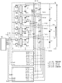
図7はこの発明の実施の形態5によるDC/DC電力変換装置の回路構成を示すものである。
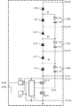
図7に示すように、DC/DC電力変換装置は、それぞれ複数段(この場合4段)の回路A1〜A4から成る3つの列回路X、Y、Zと、駆動用電源Vs1と、入出力電圧を平滑化し、またエネルギ移行のための電圧源としても機能する平滑コンデンサCs1、Cs2、Cs3、Cs4と、制御回路130と、入出力電圧端子Vcom、VL、VHとから構成される。そして、電圧端子VLとVcom間に入力された電圧V1を、約4倍に昇圧された電圧V2にして電圧端子VHとVcom間に出力する機能を有する。
Embodiment 5 FIG.
Next, a DC / DC power conversion apparatus according to Embodiment 5 of the present invention will be described.
FIG. 7 shows a circuit configuration of a DC / DC power converter according to Embodiment 5 of the present invention.
As shown in FIG. 7, the DC / DC power conversion apparatus includes three column circuits X, Y, Z each composed of a plurality of stages (four stages in this case) A1 to A4, a driving power source Vs1, and an input / output. It comprises smoothing capacitors Cs1, Cs2, Cs3, Cs4 that smooth the voltage and also function as a voltage source for energy transfer, a
各列回路X、Y、Zは、それぞれ、電圧端子VLとVcom間に入力された電圧V1を、約4倍に昇圧された電圧V2にして電圧端子VHとVcom間に出力する機能を有するDC/DCコンバータで、各列回路の構成について以下に説明する。便宜上、列回路X内の回路構成のみ図示したが、列回路Y、Zの構成も同様である。
図7に示すように、4段の回路の内、回路A1は、上記実施の形態1と同様に、低圧側素子、高圧側素子としての2つのMOSFET(Mos1L、Mos1H)を直列接続して平滑コンデンサCs1の両端子間に接続して構成される駆動用インバータ回路である。回路A2〜A4は、低圧側素子、高圧側素子として2つのダイオード(Di2L、Di2H)(Di3L、Di3H)(Di4L、Di4H)をそれぞれ直列接続して各平滑コンデンサCs2、Cs3、Cs4の両端子間に接続して構成される整流回路である。
Each column circuit X, Y, Z has a function of outputting the voltage V1 input between the voltage terminals VL and Vcom to the voltage V2 boosted about four times and outputting it between the voltage terminals VH and Vcom. A configuration of each column circuit in the / DC converter will be described below. For convenience, only the circuit configuration in the column circuit X is shown, but the configuration of the column circuits Y and Z is the same.
As shown in FIG. 7, among the four-stage circuits, the circuit A1 is smoothed by connecting two MOSFETs (Mos1L, Mos1H) as low-voltage side elements and high-voltage side elements in series as in the first embodiment. This is a drive inverter circuit configured to be connected between both terminals of the capacitor Cs1. Circuits A2 to A4 consist of two diodes (Di2L, Di2H) (Di3L, Di3H) (Di4L, Di4H) connected in series as low-voltage side elements and high-voltage side elements, and between the terminals of each smoothing capacitor Cs2, Cs3, Cs4 The rectifier circuit is configured to be connected to the rectifier.
4段の回路A1、A2、A3、A4は直列接続され、各回路A1、A2、A3、A4内の2つの素子(MOSFETあるいはダイオード)の接続点を中間端子として、所定の1回路となる駆動用インバータ回路A1と他の各整流回路A2、A3、A4との中間端子間に、コンデンサCr12、Cr13、Cr14およびインダクタLr12、Lr13、Lr14の直列体で構成されエネルギ移行素子として機能するLC直列体LC12、LC13、LC14を接続する。各段のインダクタLrとコンデンサCrのインダクタンス値と容量値から定まる共振周期の値は、それぞれ等しくなるように設定されている。
なお、各MOSFETは、ソース、ドレイン間に寄生ダイオードが形成されているパワーMOSFETである。
The four-stage circuits A1, A2, A3, A4 are connected in series, and a drive that becomes a predetermined circuit with the connection point of two elements (MOSFET or diode) in each circuit A1, A2, A3, A4 as an intermediate terminal LC series body consisting of a series body of capacitors Cr12, Cr13, Cr14 and inductors Lr12, Lr13, Lr14 between the intermediate terminals of the inverter circuit A1 and the other rectifier circuits A2, A3, A4 and functioning as an energy transfer element Connect LC12, LC13, and LC14. The resonance period values determined from the inductance value and the capacitance value of the inductor Lr and the capacitor Cr at each stage are set to be equal to each other.
Each MOSFET is a power MOSFET in which a parasitic diode is formed between the source and drain.
また、列回路X(Y、Z)は、回路A1内のMOSFETを駆動するための、ゲート駆動回路111およびフォトカプラ121L、121Hを備える。さらに、ゲート信号入力端子Tm−GL、Tm−GHと、電源入力端子あるいは平滑コンデンサ接続端子となるTm−Com、Tm−Vs1、Tm−Cs1〜Tm−Cs4を備える。
各列回路X、Y、Zで共有する電源Vs1は、Mos1Lのソース端子を基準とした、各列回路X、Y、Z内のMOSFET、ゲート駆動回路111およびフォトカプラ121L、121Hを駆動するために備えられた電源である。
制御回路130から各列回路X、Y、Z毎にゲート信号(GateL−X、GateH−X)、(GateL−Y、GateH−Y)、(GateL−Z、GateH−Z)が出力され、これらゲート信号により各列回路X、Y、Zが駆動される。
The column circuit X (Y, Z) includes a
The power supply Vs1 shared by the column circuits X, Y, and Z drives the MOSFETs, the
A gate signal (GateL-X, GateH-X), (GateL-Y, GateH-Y), (GateL-Z, GateH-Z) is output from the
次に、動作について説明する。
平滑コンデンサCs1、Cs2、Cs3、Cs4の容量値は、LC直列体LC12、LC13、LC14のコンデンサCrの容量値と比較して十分大きな値に設定される。電圧端子VL−Vcom間に入力された電圧V1を、約4倍に昇圧された電圧V2にして電圧端子VH−Vcom間に出力するため、電圧端子VH−Vcom間に負荷が接続され、電圧V2は4×V1よりも低い値となっている。定常状態では、平滑コンデンサCs1には電圧V1の電圧が充電されており、平滑コンデンサCs2、Cs3、Cs4には平均的に(V2−V1)/3の電圧が充電されている。
駆動用インバータ回路A1は、電圧端子VL−Vcom間に入力されるエネルギを、MOSFET(Mos1L、Mos1H)のオンオフ動作により高電圧側に送り、整流回路A2〜A4は、駆動用インバータ回路A1で駆動された電流を整流し、エネルギを高電圧側へ移行する。
Next, the operation will be described.
The capacitance values of the smoothing capacitors Cs1, Cs2, Cs3, and Cs4 are set to a sufficiently large value as compared with the capacitance value of the capacitor Cr of the LC series bodies LC12, LC13, and LC14. Since the voltage V1 input between the voltage terminals VL and Vcom is changed to a voltage V2 boosted about four times and output between the voltage terminals VH and Vcom, a load is connected between the voltage terminals VH and Vcom, and the voltage V2 Is lower than 4 × V1. In the steady state, the smoothing capacitor Cs1 is charged with the voltage V1, and the smoothing capacitors Cs2, Cs3, and Cs4 are charged with an average voltage of (V2−V1) / 3.
The driving inverter circuit A1 sends energy input between the voltage terminals VL and Vcom to the high voltage side by the on / off operation of the MOSFETs (Mos1L, Mos1H), and the rectifier circuits A2 to A4 are driven by the driving inverter circuit A1. The rectified current is rectified, and energy is transferred to the high voltage side.
2つのMOSFET(Mos1L、Mos1H)へのゲート信号GateL(GateL−X、GateL−Y、GateL−Z)、GateH(GateH−X、GateH−Y、GateH−Z)は、上記実施の形態1と同様に生成されるが、上記実施の形態1では整流回路内のMOSFETのソースからドレインに流れていた電流が、この実施の形態では整流回路A2〜A4内の各ダイオードを順方向に流れる。
低圧側MOSFETへのゲート信号GateLにより駆動用インバータ回路A1のMos1Lがオン状態となると、電圧差があるため、平滑コンデンサCs1、Cs2、Cs3に蓄えられた一部のエネルギが、以下に示す経路でコンデンサCr12、Cr13、Cr14に移行する。
Cs1⇒Di2L⇒Lr12⇒Cr12⇒Mos1L
Cs1⇒Cs2⇒Di3L⇒Lr13⇒Cr13⇒Mos1L
Cs1⇒Cs2⇒Cs3⇒Di4L⇒Lr14⇒Cr14⇒Mos1L
The gate signals GateL (GateL-X, GateL-Y, GateL-Z) and GateH (GateH-X, GateH-Y, GateH-Z) to the two MOSFETs (Mos1L, Mos1H) are the same as in the first embodiment. In the first embodiment, the current flowing from the source to the drain of the MOSFET in the rectifier circuit flows in the forward direction in each diode in the rectifier circuits A2 to A4.
When Mos1L of the drive inverter circuit A1 is turned on by the gate signal GateL to the low-voltage side MOSFET, there is a voltage difference, so that part of the energy stored in the smoothing capacitors Cs1, Cs2, and Cs3 passes through the following path Transition to capacitors Cr12, Cr13, Cr14.
Cs1⇒Di2L⇒Lr12⇒Cr12⇒Mos1L
Cs1⇒Cs2⇒Di3L⇒Lr13⇒Cr13⇒Mos1L
Cs1⇒Cs2⇒Cs3⇒Di4L⇒Lr14⇒Cr14⇒Mos1L
次いで、高圧側MOSFETへのゲート信号GateHにより駆動用インバータ回路A1のMos1Hがオン状態となると、電圧差があるため、コンデンサCr12、Cr13、Cr14に充電されたエネルギが、以下に示す経路で平滑コンデンサCs2、Cs3、Cs4に移行する。
Cr12⇒Lr12⇒Di2H⇒Cs2⇒Mos1H
Cr13⇒Lr13⇒Di3H⇒Cs3⇒Cs2⇒Mos1H
Cr14⇒Lr14⇒Di4H⇒Cs4⇒Cs3⇒Cs2⇒Mos1H
Next, when Mos1H of the driving inverter circuit A1 is turned on by the gate signal GateH to the high-voltage side MOSFET, there is a voltage difference, so that the energy charged in the capacitors Cr12, Cr13, Cr14 is smoothed by the path shown below. Move to Cs2, Cs3, Cs4.
Cr12⇒Lr12⇒Di2H⇒Cs2⇒Mos1H
Cr13⇒Lr13⇒Di3H⇒Cs3⇒Cs2⇒Mos1H
Cr14⇒Lr14⇒Di4H⇒Cs4⇒Cs3⇒Cs2⇒Mos1H
このように、コンデンサCr12、Cr13、Cr14の充放電により、平滑コンデンサCs1から平滑コンデンサCs2、Cs3、Cs4にエネルギを移行する。そして、電圧端子VLとVcom間に入力された電圧V1を、約4倍に昇圧された電圧V2にして電圧端子VHとVcom間に出力する。また、各コンデンサCr12、Cr13、Cr14には、インダクタLr12、Lr13、Lr14が直列に接続されてLC直列体LC12、LC13、LC14を構成するため、上記エネルギの移行は共振現象を利用したものとなり、大きなエネルギ量を効率よく移行できる。 In this way, energy is transferred from the smoothing capacitor Cs1 to the smoothing capacitors Cs2, Cs3, and Cs4 by charging and discharging the capacitors Cr12, Cr13, and Cr14. Then, the voltage V1 input between the voltage terminals VL and Vcom is changed to a voltage V2 boosted about four times and output between the voltage terminals VH and Vcom. Also, inductors Lr12, Lr13, Lr14 are connected in series to each capacitor Cr12, Cr13, Cr14 to form an LC series body LC12, LC13, LC14, so the above energy transfer uses a resonance phenomenon, A large amount of energy can be transferred efficiently.
また、各LC直列体LC12、LC13、LC14に流れる電流I12、I13、I14も上記実施の形態1の場合とほぼ同様である。即ち、この実施の形態においても、上記実施の形態1と同様に、駆動用インバータ回路A1と他の各整流回路A2〜A4との中間端子間にLC直列体LC12、LC13、LC14を接続したため、上記実施の形態1と同様に、エネルギ移行用のLC直列体LC12、LC13、LC14のインダクタLr、コンデンサCrの電流定格を低下させ、インダクタLrとコンデンサCrを小形化することができる。
また、この実施の形態では、整流回路A2〜A4にダイオードを用いたため、MOSFETを用いたものに比して導通損失が増大するが、駆動用の電源や回路が不要になる。
Further, the currents I12, I13, and I14 flowing through the LC serial bodies LC12, LC13, and LC14 are substantially the same as those in the first embodiment. That is, in this embodiment, as in the first embodiment, the LC series bodies LC12, LC13, and LC14 are connected between the intermediate terminals of the driving inverter circuit A1 and the other rectifier circuits A2 to A4. As in the first embodiment, the current ratings of the inductor Lr and the capacitor Cr of the LC series bodies LC12, LC13, and LC14 for energy transfer can be reduced, and the inductor Lr and the capacitor Cr can be reduced in size.
In this embodiment, since diodes are used for the rectifier circuits A2 to A4, the conduction loss is increased as compared with the case where MOSFETs are used, but a driving power supply and circuit are not required.
以上のように各列回路X、Y、Zは動作するものであるが、各列回路X、Y、Zを駆動する駆動信号は、上記実施の形態1と同様に、周期をT(LC直列体にて定まる共振周期)として一致させると共に、各列回路間で位相をT/3(2π/3(rad))ずつずらして駆動する(図3参照)。また、3つの列回路X、Y、Zは、列回路内の各回路A1、A2、A3、A4に並列配置される平滑コンデンサCs1、Cs2、Cs3、Cs4を共有して並列接続される。これにより、平滑コンデンサCs1、Cs2、Cs3、Cs4の充放電タイミングがずれ、平滑コンデンサCs1、Cs2、Cs3、Cs4への充放電電流を列回路間で融通し合うため、平滑コンデンサCs1、Cs2、Cs3、Cs4に流れる交流電流(リプル電流)が低減する。このような平滑コンデンサのリプル電流低減により、上記実施の形態1と同様に、信頼性の向上、電力変換効率の向上、および装置構成の小型化が図れる。 As described above, each column circuit X, Y, Z operates, but the drive signal for driving each column circuit X, Y, Z has a cycle of T (LC series) as in the first embodiment. (Resonance period determined by the body) and the phase is shifted by T / 3 (2π / 3 (rad)) between the column circuits (see FIG. 3). The three column circuits X, Y, and Z are connected in parallel by sharing smoothing capacitors Cs1, Cs2, Cs3, and Cs4 arranged in parallel with the circuits A1, A2, A3, and A4 in the column circuit. As a result, the charging / discharging timing of the smoothing capacitors Cs1, Cs2, Cs3, Cs4 is shifted, and the charging / discharging currents to the smoothing capacitors Cs1, Cs2, Cs3, Cs4 are interchanged between the column circuits, so that the smoothing capacitors Cs1, Cs2, Cs3 , AC current (ripple current) flowing through Cs4 is reduced. By reducing the ripple current of such a smoothing capacitor, as in the first embodiment, it is possible to improve reliability, improve power conversion efficiency, and reduce the size of the device configuration.
なお、この実施の形態においても、列回路の個数および位相差は上述したものに限らず、列回路を複数(n個)配列して位相を各列回路間でずらして駆動することにより、平滑コンデンサCs1、Cs2、Cs3、Cs4のリプル電流が減少する効果が得られる。また、各列回路の位相を2π/n(rad)ずつずらすのが最も効果的であり、さらに、列回路の数nを増加するほど平滑コンデンサCs1、Cs2、Cs3、Cs4のリプル電流が低減できる。 In this embodiment, the number of column circuits and the phase difference are not limited to those described above, and a plurality of (n) column circuits are arranged and driven by shifting the phase between the column circuits. An effect of reducing the ripple current of the capacitors Cs1, Cs2, Cs3, and Cs4 can be obtained. Further, it is most effective to shift the phase of each column circuit by 2π / n (rad), and the ripple current of the smoothing capacitors Cs1, Cs2, Cs3, and Cs4 can be reduced as the number n of column circuits is increased. .
実施の形態6.
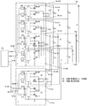
次に、この発明の実施の形態6によるDC/DC電力変換装置について説明する。
この実施の形態によるDC/DC電力変換装置の回路構成は、上記実施の形態5における図7で示す回路構成において、各列回路X、Y、Zの構成が異なるもので、各列回路X、Y、Zの回路構成を図8に示す。その他の構成は図7と同様である。
上記実施の形態5と同様に、各列回路X、Y、Zは、それぞれ、電圧端子VLとVcom間に入力された電圧V1を、約4倍に昇圧された電圧V2にして電圧端子VHとVcom間に出力する機能を有するDC/DCコンバータで、複数段(この場合4段)の回路A1〜A4から構成される。
Next, a DC / DC power converter according to
The circuit configuration of the DC / DC power converter according to this embodiment is different from the circuit configuration shown in FIG. 7 in the fifth embodiment in the configuration of each column circuit X, Y, Z. A circuit configuration of Y and Z is shown in FIG. Other configurations are the same as those in FIG.
As in the fifth embodiment, each of the column circuits X, Y, and Z converts the voltage V1 input between the voltage terminals VL and Vcom to the voltage V2 boosted by about four times and the voltage terminal VH. This is a DC / DC converter having a function of outputting between Vcom and is composed of a plurality of stages (in this case, four stages) of circuits A1 to A4.
図8に示すように、4段の回路の内、回路A1は、上記実施の形態5と同様に、低圧側素子、高圧側素子としての2つのMOSFET(Mos1L、Mos1H)を直列接続して平滑コンデンサCs1の両端子間に接続して構成される駆動用インバータ回路である。回路A2〜A4は、低圧側素子、高圧側素子として2つのダイオード(Di2L、Di2H)(Di3L、Di3H)(Di4L、Di4H)をそれぞれ直列接続して各平滑コンデンサCs2、Cs3、Cs4の両端子間に接続して構成される整流回路である(図7参照)。そして、4段の回路A1、A2、A3、A4は直列接続され、各回路A1、A2、A3、A4内の2つの素子(MOSFETあるいはダイオード)の接続点を中間端子として、隣接する各回路、即ち(A1,A2)(A2,A3)(A3,A4)の中間端子間に、コンデンサCr12、Cr23、Cr34およびインダクタLr12、Lr23、Lr34の直列体で構成されエネルギ移行素子として機能するLC直列体LC12、LC23、LC34を接続する。各段のインダクタLrとコンデンサCrのインダクタンス値と容量値から定まる共振周期の値は、それぞれ等しくなるように設定されている。 As shown in FIG. 8, among the four-stage circuits, the circuit A1 is smoothed by connecting two MOSFETs (Mos1L, Mos1H) as low voltage side elements and high voltage side elements in series as in the fifth embodiment. This is a drive inverter circuit configured to be connected between both terminals of the capacitor Cs1. Circuits A2 to A4 consist of two diodes (Di2L, Di2H) (Di3L, Di3H) (Di4L, Di4H) connected in series as low-voltage side elements and high-voltage side elements, and between the terminals of each smoothing capacitor Cs2, Cs3, Cs4 (See FIG. 7). Then, the four-stage circuits A1, A2, A3, A4 are connected in series, and adjacent circuits with the connection point of two elements (MOSFET or diode) in each circuit A1, A2, A3, A4 as an intermediate terminal, That is, an LC series body composed of capacitors Cr12, Cr23, Cr34 and inductors Lr12, Lr23, Lr34 in series between the intermediate terminals of (A1, A2) (A2, A3) (A3, A4) and functioning as an energy transfer element Connect LC12, LC23, and LC34. The resonance period values determined from the inductance value and the capacitance value of the inductor Lr and the capacitor Cr at each stage are set to be equal to each other.
また、回路A1内のMOSFETを駆動するための、ゲート駆動回路111およびフォトカプラ121L、121Hを備える。さらに、ゲート信号入力端子Tm−GL、Tm−GHと、電源入力端子あるいは平滑コンデンサ接続端子となるTm−Com、Tm−Vs1、Tm−Cs1〜Tm−Cs4を備える。
なお、各MOSFETは、ソース、ドレイン間に寄生ダイオードが形成されているパワーMOSFETである。
Further, a
Each MOSFET is a power MOSFET in which a parasitic diode is formed between the source and drain.
次に、動作について説明する。
平滑コンデンサCs1、Cs2、Cs3、Cs4の容量値は、LC直列体LC12、LC13、LC14のコンデンサCrの容量値と比較して十分大きな値に設定される。電圧端子VL−Vcom間に入力された電圧V1を、約4倍に昇圧された電圧V2にして電圧端子VH−Vcom間に出力するため、電圧端子VH−Vcom間に負荷が接続され、電圧V2は4×V1よりも低い値となっている。定常状態では、平滑コンデンサCs1には電圧V1の電圧が充電されており、平滑コンデンサCs2、Cs3、Cs4には平均的に(V2−V1)/3の電圧が充電されている。
駆動用インバータ回路A1は、電圧端子VL−Vcom間に入力されるエネルギを、MOSFET(Mos1L、Mos1H)のオンオフ動作により高電圧側に送り、整流回路A2〜A4は、駆動用インバータ回路A1で駆動された電流を整流し、エネルギを高電圧側へ移行する。
Next, the operation will be described.
The capacitance values of the smoothing capacitors Cs1, Cs2, Cs3, and Cs4 are set to a sufficiently large value as compared with the capacitance value of the capacitor Cr of the LC series bodies LC12, LC13, and LC14. Since the voltage V1 input between the voltage terminals VL and Vcom is changed to a voltage V2 boosted about four times and output between the voltage terminals VH and Vcom, a load is connected between the voltage terminals VH and Vcom, and the voltage V2 Is lower than 4 × V1. In the steady state, the smoothing capacitor Cs1 is charged with the voltage V1, and the smoothing capacitors Cs2, Cs3, and Cs4 are charged with an average voltage of (V2−V1) / 3.
The drive inverter circuit A1 sends the energy input between the voltage terminals VL and Vcom to the high voltage side by the on / off operation of the MOSFETs (Mos1L, Mos1H), and the rectifier circuits A2 to A4 are driven by the drive inverter circuit A1. The rectified current is rectified, and energy is transferred to the high voltage side.
2つのMOSFET(Mos1L、Mos1H)へのゲート信号GateL(GateL−X、GateL−Y、GateL−Z)、GateH(GateH−X、GateH−Y、GateH−Z)は、上記実施の形態1と同様に生成されるが、上記実施の形態1では整流回路内のMOSFETのソースからドレインに流れていた電流が、この実施の形態では整流回路A2〜A4内の各ダイオードを順方向に流れる。
低圧側MOSFETへのゲート信号GateLにより駆動用インバータ回路A1のMos1Lがオン状態となると、電圧差があるため、平滑コンデンサCs1、Cs2、Cs3に蓄えられた一部のエネルギが、以下に示す経路でコンデンサCr12、Cr23、Cr34に移行する。
Cs1⇒Di2L⇒Lr12⇒Cr12⇒Mos1L
Cs1⇒Cs2⇒Di3L⇒Lr23⇒Cr23⇒Lr12⇒Cr12⇒Mos1L
Cs1⇒Cs2⇒Cs3⇒Di4L⇒Lr34⇒Cr34⇒Lr23⇒Cr23⇒Lr12⇒Cr12⇒Mos1L
The gate signals GateL (GateL-X, GateL-Y, GateL-Z) and GateH (GateH-X, GateH-Y, GateH-Z) to the two MOSFETs (Mos1L, Mos1H) are the same as in the first embodiment. In the first embodiment, the current flowing from the source to the drain of the MOSFET in the rectifier circuit flows in the forward direction in each diode in the rectifier circuits A2 to A4.
When Mos1L of the drive inverter circuit A1 is turned on by the gate signal GateL to the low-voltage side MOSFET, there is a voltage difference, so that part of the energy stored in the smoothing capacitors Cs1, Cs2, and Cs3 passes through the following path Transition to capacitors Cr12, Cr23, Cr34.
Cs1⇒Di2L⇒Lr12⇒Cr12⇒Mos1L
Cs1⇒Cs2⇒Di3L⇒Lr23⇒Cr23⇒Lr12⇒Cr12⇒Mos1L
Cs1⇒Cs2⇒Cs3⇒Di4L⇒Lr34⇒Cr34⇒Lr23⇒Cr23⇒Lr12⇒Cr12⇒Mos1L
次いで、高圧側MOSFETへのゲート信号GateHにより駆動用インバータ回路A1のMos1Hがオン状態となると、電圧差があるため、コンデンサCr12、Cr23、Cr34に充電されたエネルギが、以下に示す経路で平滑コンデンサCs2、Cs3、Cs4に移行する。
Mos1H⇒Cr12⇒Lr12⇒Di2H⇒Cs2
Mos1H⇒Cr12⇒Lr12⇒Cr23⇒Lr23⇒Di3H⇒Cs3⇒Cs2
Mos1H⇒Cr12⇒Lr12⇒Cr23⇒Lr23⇒Cr34⇒Lr34⇒Di4H⇒Cs4⇒Cs3⇒Cs2
Next, when Mos1H of the driving inverter circuit A1 is turned on by the gate signal GateH to the high-voltage side MOSFET, there is a voltage difference, so that the energy charged in the capacitors Cr12, Cr23, and Cr34 is smoothed by the path shown below. Move to Cs2, Cs3, Cs4.
Mos1H⇒Cr12⇒Lr12⇒Di2H⇒Cs2
Mos1H⇒Cr12⇒Lr12⇒Cr23⇒Lr23⇒Di3H⇒Cs3⇒Cs2
Mos1H⇒Cr12⇒Lr12⇒Cr23⇒Lr23⇒Cr34⇒Lr34⇒Di4H⇒Cs4⇒Cs3⇒Cs2
このように、コンデンサCr12、Cr23、Cr34の充放電により、平滑コンデンサCs1から平滑コンデンサCs2、Cs3、Cs4にエネルギを移行する。そして、電圧端子VLとVcom間に入力された電圧V1を、約4倍に昇圧された電圧V2にして電圧端子VHとVcom間に出力する。また、各コンデンサCr12、Cr23、Cr34には、インダクタLr12、Lr23、Lr34が直列に接続されてLC直列体LC12、LC23、LC34を構成するため、上記エネルギの移行は共振現象を利用したものとなり、大きなエネルギ量を効率よく移行できる。 As described above, energy is transferred from the smoothing capacitor Cs1 to the smoothing capacitors Cs2, Cs3, and Cs4 by charging and discharging the capacitors Cr12, Cr23, and Cr34. Then, the voltage V1 input between the voltage terminals VL and Vcom is changed to a voltage V2 boosted about four times and output between the voltage terminals VH and Vcom. Also, inductors Lr12, Lr23, Lr34 are connected in series to each capacitor Cr12, Cr23, Cr34 to form an LC series body LC12, LC23, LC34, so that the energy transfer utilizes a resonance phenomenon, A large amount of energy can be transferred efficiently.
また、この実施の形態では、隣接する回路間にLC直列体LC12、LC23、LC34を接続したため、駆動用インバータ回路A1と他の各整流回路A2〜A4との間にLC直列体LC12、LC13、LC14を接続した場合と比較すると、各LC直列体を流れる電流は増大するが、コンデンサCr34の印加電圧がコンデンサCr14の1/3、コンデンサCr23の印加電圧がコンデンサCr13の1/2に低減できる効果がある。
また、整流回路A2〜A4にダイオードを用いたため、MOSFETを用いたものに比して導通損失が増大するが、駆動用の電源や回路が不要になる。
In this embodiment, since the LC series bodies LC12, LC23, and LC34 are connected between adjacent circuits, the LC series bodies LC12, LC13, LC13, LC are connected between the driving inverter circuit A1 and the other rectifier circuits A2 to A4. Compared with the case where LC14 is connected, the current flowing through each LC series increases, but the applied voltage of capacitor Cr34 can be reduced to 1/3 of capacitor Cr14 and the applied voltage of capacitor Cr23 to 1/2 of capacitor Cr13. There is.
In addition, since diodes are used for the rectifier circuits A2 to A4, conduction loss is increased as compared with those using MOSFETs, but a driving power supply and circuit are not required.
以上のように各列回路X、Y、Zは動作するものであるが、各列回路X、Y、Zを駆動する駆動信号は、上記実施の形態1と同様に、周期をT(LC直列体にて定まる共振周期)として一致させると共に、各列回路間で位相をT/3(2π/3(rad))ずつずらして駆動する(図3参照)。また、3つの列回路X、Y、Zは、列回路内の各回路A1、A2、A3、A4に並列配置される平滑コンデンサCs1、Cs2、Cs3、Cs4を共有して並列接続される。これにより、平滑コンデンサCs1、Cs2、Cs3、Cs4の充放電タイミングがずれ、平滑コンデンサCs1、Cs2、Cs3、Cs4への充放電電流を列回路間で融通し合うため、平滑コンデンサCs1、Cs2、Cs3、Cs4に流れる交流電流(リプル電流)が低減する。このような平滑コンデンサのリプル電流低減により、上記実施の形態1と同様に、信頼性の向上、電力変換効率の向上、および装置構成の小型化が図れる。 As described above, each column circuit X, Y, Z operates, but the drive signal for driving each column circuit X, Y, Z has a cycle of T (LC series) as in the first embodiment. (Resonance period determined by the body) and the phase is shifted by T / 3 (2π / 3 (rad)) between the column circuits (see FIG. 3). The three column circuits X, Y, and Z are connected in parallel by sharing smoothing capacitors Cs1, Cs2, Cs3, and Cs4 arranged in parallel with the circuits A1, A2, A3, and A4 in the column circuit. As a result, the charging / discharging timing of the smoothing capacitors Cs1, Cs2, Cs3, Cs4 is shifted, and the charging / discharging currents to the smoothing capacitors Cs1, Cs2, Cs3, Cs4 are interchanged between the column circuits, so that the smoothing capacitors Cs1, Cs2, Cs3 , AC current (ripple current) flowing through Cs4 is reduced. By reducing the ripple current of such a smoothing capacitor, as in the first embodiment, it is possible to improve reliability, improve power conversion efficiency, and reduce the size of the device configuration.
なお、この実施の形態においても、列回路の個数および位相差は上述したものに限らず、列回路を複数(n個)配列して位相を各列回路間でずらして駆動することにより、平滑コンデンサCs1、Cs2、Cs3、Cs4のリプル電流が減少する効果が得られる。また、各列回路の位相を2π/n(rad)ずつずらすのが最も効果的であり、さらに、列回路の数nを増加するほど平滑コンデンサCs1、Cs2、Cs3、Cs4のリプル電流が低減できる。 In this embodiment, the number of column circuits and the phase difference are not limited to those described above, and a plurality of (n) column circuits are arranged and driven by shifting the phase between the column circuits. An effect of reducing the ripple current of the capacitors Cs1, Cs2, Cs3, and Cs4 can be obtained. Further, it is most effective to shift the phase of each column circuit by 2π / n (rad), and the ripple current of the smoothing capacitors Cs1, Cs2, Cs3, and Cs4 can be reduced as the number n of column circuits is increased. .
実施の形態7.
次に、この発明の実施の形態7によるDC/DC電力変換装置について説明する。
図9はこの発明の実施の形態7によるDC/DC電力変換装置の回路構成を示すものである。
図9に示すように、DC/DC電力変換装置は、それぞれ複数段(この場合4段)の回路A1〜A4から成る3つの列回路X、Y、Zと、駆動用電源Vs2〜Vs4と、入出力電圧を平滑化し、またエネルギ移行のための電圧源としても機能する平滑コンデンサCs1、Cs2、Cs3、Cs4と、制御回路130と、入出力電圧端子Vcom、VL、VHとから構成される。そして、電圧端子VH−Vcom間に入力された電圧V2を、約1/4倍に降圧された電圧V1にして電圧端子VL−Vcom間に出力する機能を有する。
Embodiment 7 FIG.
Next, a DC / DC power converter according to Embodiment 7 of the present invention will be described.
FIG. 9 shows a circuit configuration of a DC / DC power converter according to Embodiment 7 of the present invention.
As shown in FIG. 9, the DC / DC power converter includes three column circuits X, Y, and Z each including a plurality of stages (four stages in this case) of circuits A1 to A4, driving power supplies Vs2 to Vs4, It comprises smoothing capacitors Cs1, Cs2, Cs3, Cs4 that smooth the input / output voltage and also function as a voltage source for energy transfer, a
各列回路X、Y、Zは、それぞれ、電圧端子VH−Vcom間に入力された電圧V2を、約1/4倍に降圧された電圧V1にして電圧端子VL−Vcom間に出力する機能を有するDC/DCコンバータで、各列回路の構成について以下に説明する。便宜上、列回路X内の回路構成のみ図示したが、列回路Y、Zの構成も同様である。
図9に示すように、4段の回路の内、回路A2〜A4は、低圧側素子、高圧側素子としての2つのMOSFET(Mos2L、Mos2H)(Mos3L、Mos3H)(Mos4L、Mos4H)を直列接続して、各平滑コンデンサCs2、Cs3、Cs4の両端子間に接続して構成される駆動用インバータ回路である。また回路A1は、低圧側素子、高圧側素子としての2つのダイオード(Di1L、Di1H)を直列接続して平滑コンデンサCs1の両端子間に接続して構成される整流回路である。
Each of the column circuits X, Y, and Z has a function of converting the voltage V2 input between the voltage terminals VH and Vcom to a voltage V1 that is stepped down by about 1/4 to output between the voltage terminals VL and Vcom. The configuration of each column circuit in the DC / DC converter having the above will be described below. For convenience, only the circuit configuration in the column circuit X is shown, but the configuration of the column circuits Y and Z is the same.
As shown in FIG. 9, among the four-stage circuits, the circuits A2 to A4 are two MOSFETs (Mos2L, Mos2H) (Mos3L, Mos3H) (Mos4L, Mos4H) connected in series as the low voltage side element and the high voltage side element. Thus, the driving inverter circuit is configured to be connected between both terminals of the smoothing capacitors Cs2, Cs3, and Cs4. The circuit A1 is a rectifier circuit configured by connecting two diodes (Di1L, Di1H) as low-voltage side elements and high-voltage side elements in series and connecting between both terminals of the smoothing capacitor Cs1.
4段の回路A1、A2、A3、A4は直列接続され、各回路A1、A2、A3、A4内の2つの素子(MOSFETあるいはダイオード)の接続点を中間端子として、所定の1回路となる整流回路A1と他の各駆動用インバータ回路A2、A3、A4との中間端子間に、コンデンサCr12、Cr13、Cr14およびインダクタLr12、Lr13、Lr14の直列体で構成されエネルギ移行素子として機能するLC直列体LC12、LC13、LC14を接続する。各段のインダクタLrとコンデンサCrのインダクタンス値と容量値から定まる共振周期の値は、それぞれ等しくなるように設定されている。
なお、各MOSFETは、ソース、ドレイン間に寄生ダイオードが形成されているパワーMOSFETである。
The four-stage circuits A1, A2, A3, A4 are connected in series, and a rectification that forms a predetermined circuit with the connection point of two elements (MOSFET or diode) in each circuit A1, A2, A3, A4 as an intermediate terminal LC series body composed of a series body of capacitors Cr12, Cr13, Cr14 and inductors Lr12, Lr13, Lr14 between the intermediate terminals of the circuit A1 and the other driving inverter circuits A2, A3, A4 and functioning as an energy transfer element Connect LC12, LC13, and LC14. The resonance period values determined from the inductance value and the capacitance value of the inductor Lr and the capacitor Cr at each stage are set to be equal to each other.
Each MOSFET is a power MOSFET in which a parasitic diode is formed between the source and drain.
また、列回路X(Y、Z)は、駆動用インバータ回路A2〜A4内のMOSFETを駆動するための、ゲート駆動回路112〜114およびフォトカプラ(122L、122H)〜(124L、124H)を備える。さらに、ゲート信号入力端子Tm−GL、Tm−GHと、電源入力端子あるいは平滑コンデンサ接続端子となるTm−Com、Tm−Vs2〜Tm−Vs4、Tm−Cs1〜Tm−Cs4を備える。
各列回路X、Y、Zで共有する電源Vs2、Vs3、Vs4は、それぞれMos2L、Mos3L、Mos4Lのソース端子を基準とした、各列回路X、Y、Z内のMOSFET、ゲート駆動回路112〜114およびフォトカプラ(122L、122H)〜(124L、124H)を駆動するために備えられた電源である。
制御回路130から各列回路X、Y、Z毎にゲート信号(GateL−X、GateH−X)、(GateL−Y、GateH−Y)、(GateL−Z、GateH−Z)が出力され、これらゲート信号により各列回路X、Y、Zが駆動される。
The column circuit X (Y, Z) includes
The power sources Vs2, Vs3, and Vs4 shared by the column circuits X, Y, and Z are the MOSFETs in the column circuits X, Y, and Z, and the
A gate signal (GateL-X, GateH-X), (GateL-Y, GateH-Y), (GateL-Z, GateH-Z) is output from the
次に、動作について説明する。
各列回路X、Y、Zの動作について以下に説明する。
平滑コンデンサCs1、Cs2、Cs3、Cs4の容量値は、LC直列体のコンデンサCr12、Cr13、Cr14の容量値と比較して十分大きな値に設定される。各列回路X、Y、Zは、それぞれ電圧端子VH−Vcom間に入力された電圧V2を、約1/4倍に降圧された電圧V1にして電圧端子VL−Vcom間に出力する機能を有するDC/DCコンバータであるため、電圧端子VL−Vcom間に負荷が接続され、電圧V2は4×V1よりも高い値となっている。定常状態では、平滑コンデンサCs1には電圧V1の電圧が充電されており、平滑コンデンサCs2、Cs3、Cs4には平均的に(V2−V1)/3の電圧が充電されている。
Next, the operation will be described.
The operation of each column circuit X, Y, Z will be described below.
The capacitance values of the smoothing capacitors Cs1, Cs2, Cs3, and Cs4 are set to a sufficiently large value as compared with the capacitance values of the LC series capacitors Cr12, Cr13, and Cr14. Each of the column circuits X, Y, and Z has a function of converting the voltage V2 input between the voltage terminals VH and Vcom into a voltage V1 stepped down by about 1/4 and outputting the voltage V1 between the voltage terminals VL and Vcom. Since it is a DC / DC converter, a load is connected between the voltage terminals VL and Vcom, and the voltage V2 is higher than 4 × V1. In the steady state, the smoothing capacitor Cs1 is charged with the voltage V1, and the smoothing capacitors Cs2, Cs3, and Cs4 are charged with an average voltage of (V2−V1) / 3.
駆動用インバータ回路A2〜A4内のMOSFETへのゲート信号GateL(GateL−X、GateL−Y、GateL−Z)、GateH(GateH−X、GateH−Y、GateH−Z)は、上記実施の形態2と同様に生成されるが、上記実施の形態2では整流回路A1内のMOSFETのソースからドレインに流れていた電流が、この実施の形態では整流回路A1内のダイオードを順方向に流れる。 The gate signals GateL (GateL-X, GateL-Y, GateL-Z) and GateH (GateH-X, GateH-Y, GateH-Z) to the MOSFETs in the driving inverter circuits A2 to A4 are the same as those in the second embodiment. However, the current flowing from the source to the drain of the MOSFET in the rectifier circuit A1 flows in the forward direction in the diode in the rectifier circuit A1 in this embodiment.
高圧側MOSFETへのゲート信号GateH(GateH−X、GateH−Y、GateH−Z)により各駆動用インバータ回路A2〜A4の高圧側MOSFETであるMos2H、Mos3H、Mos4Hがオン状態となると、電圧差があるため、平滑コンデンサCs2、Cs3、Cs4に蓄えられた一部のエネルギが、以下に示す経路でコンデンサCr12、Cr13、Cr14に移行する。
Cs2⇒Cs3⇒Cs4⇒Mos4H⇒Lr14⇒Cr14⇒Di1H
Cs2⇒Cs3⇒Mos3H⇒Lr13⇒Cr13⇒Di1H
Cs2⇒Mos2H⇒Lr12⇒Cr12⇒Di1H
When the gate signals GateH (GateH-X, GateH-Y, GateH-Z) to the high-voltage side MOSFETs turn on the high-voltage side MOSFETs Mos2H, Mos3H, and Mos4H of the drive inverter circuits A2 to A4, the voltage difference For this reason, some energy stored in the smoothing capacitors Cs2, Cs3, and Cs4 is transferred to the capacitors Cr12, Cr13, and Cr14 through the following path.
Cs2⇒Cs3⇒Cs4⇒Mos4H⇒Lr14⇒Cr14⇒Di1H
Cs2⇒Cs3⇒Mos3H⇒Lr13⇒Cr13⇒Di1H
Cs2⇒Mos2H⇒Lr12⇒Cr12⇒Di1H
次いで、低圧側MOSFETへのゲート信号GateL(GateL−X、GateL−Y、GateL−Z)により各駆動用インバータ回路A2〜A4の低圧側MOSFETであるMos2L、Mos3L、Mos4LLがオン状態となると、電圧差があるため、コンデンサCr12、Cr13、Cr14に充電されたエネルギが、以下に示す経路で平滑コンデンサCs1、Cs2、Cs3に移行する。
Cr14⇒Lr14⇒Mos4L⇒Cs3⇒Cs2⇒Cs1⇒Di1L
Cr13⇒Lr13⇒Mos3L⇒Cs2⇒Cs1⇒Di1L
Cr12⇒Lr12⇒Mos2L⇒Cs1⇒Di1L
Next, when the gate signals GateL (GateL-X, GateL-Y, GateL-Z) to the low voltage side MOSFETs turn on the low voltage side MOSFETs Mos2L, Mos3L, Mos4LL of the driving inverter circuits A2 to A4, Due to the difference, the energy charged in the capacitors Cr12, Cr13, and Cr14 is transferred to the smoothing capacitors Cs1, Cs2, and Cs3 through the following path.
Cr14⇒Lr14⇒Mos4L⇒Cs3⇒Cs2⇒Cs1⇒Di1L
Cr13⇒Lr13⇒Mos3L⇒Cs2⇒Cs1⇒Di1L
Cr12⇒Lr12⇒Mos2L⇒Cs1⇒Di1L
このように、コンデンサCr12、Cr13、Cr14の充放電により、平滑コンデンサCs2、Cs3、Cs4から平滑コンデンサCs1にエネルギを移行する。そして、電圧端子VHとVcom間に入力された電圧V2を、約1/4倍に降圧された電圧V1にして電圧端子VLとVcom間に出力する。また、各コンデンサCr12、Cr13、Cr14には、インダクタLr12、Lr13、Lr14が直列に接続されてLC直列体LC12、LC13、LC14を構成するため、上記エネルギの移行は共振現象を利用したものとなり、大きなエネルギ量を効率よく移行できる。 As described above, energy is transferred from the smoothing capacitors Cs2, Cs3, and Cs4 to the smoothing capacitor Cs1 by charging and discharging the capacitors Cr12, Cr13, and Cr14. Then, the voltage V2 input between the voltage terminals VH and Vcom is converted to a voltage V1 that has been stepped down by about 1/4 and output between the voltage terminals VL and Vcom. Also, inductors Lr12, Lr13, Lr14 are connected in series to each capacitor Cr12, Cr13, Cr14 to form an LC series body LC12, LC13, LC14, so the above energy transfer uses a resonance phenomenon, A large amount of energy can be transferred efficiently.
またこの実施の形態においても、整流回路A1と駆動用インバータ回路である他の各回路A2、A3、A4との間に、LC直列体LC12、LC13、LC14を接続したため、上記実施の形態2と同様に、エネルギ移行用のLC直列体LC12、LC13、LC14のインダクタLr、コンデンサCrの電流定格を低下させ、インダクタLrとコンデンサCrを小形化することができる。
また、この実施の形態では、整流回路A1にダイオードを用いたため、MOSFETを用いたものに比して導通損失が増大するが、駆動用の電源や回路が不要になる。
Also in this embodiment, since the LC series bodies LC12, LC13, and LC14 are connected between the rectifier circuit A1 and the other circuits A2, A3, and A4 that are driving inverter circuits, Similarly, the current ratings of the inductor Lr and the capacitor Cr of the LC series LC12, LC13, and LC14 for energy transfer can be reduced, and the inductor Lr and the capacitor Cr can be reduced in size.
In this embodiment, since a diode is used for the rectifier circuit A1, the conduction loss is increased as compared with the case where a MOSFET is used, but a driving power supply and circuit are not required.
以上のように各列回路X、Y、Zは動作するものであるが、各列回路X、Y、Zを駆動する駆動信号は、上記実施の形態1と同様に、周期をT(LC直列体にて定まる共振周期)として一致させると共に、各列回路間で位相をT/3(2π/3(rad))ずつずらして駆動する(図3参照)。また、3つの列回路X、Y、Zは、列回路内の各回路A1、A2、A3、A4に並列配置される平滑コンデンサCs1、Cs2、Cs3、Cs4を共有して並列接続される。これにより、平滑コンデンサCs1、Cs2、Cs3、Cs4の充放電タイミングがずれ、平滑コンデンサCs1、Cs2、Cs3、Cs4への充放電電流を列回路間で融通し合うため、平滑コンデンサCs1、Cs2、Cs3、Cs4に流れる交流電流(リプル電流)が低減する。このような平滑コンデンサのリプル電流低減により、上記実施の形態1と同様に、信頼性の向上、電力変換効率の向上、および装置構成の小型化が図れる。 As described above, each column circuit X, Y, Z operates, but the drive signal for driving each column circuit X, Y, Z has a cycle of T (LC series) as in the first embodiment. (Resonance period determined by the body) and the phase is shifted by T / 3 (2π / 3 (rad)) between the column circuits (see FIG. 3). The three column circuits X, Y, and Z are connected in parallel by sharing smoothing capacitors Cs1, Cs2, Cs3, and Cs4 arranged in parallel with the circuits A1, A2, A3, and A4 in the column circuit. As a result, the charging / discharging timing of the smoothing capacitors Cs1, Cs2, Cs3, Cs4 is shifted, and the charging / discharging currents to the smoothing capacitors Cs1, Cs2, Cs3, Cs4 are interchanged between the column circuits, so that the smoothing capacitors Cs1, Cs2, Cs3 , AC current (ripple current) flowing through Cs4 is reduced. By reducing the ripple current of such a smoothing capacitor, as in the first embodiment, it is possible to improve reliability, improve power conversion efficiency, and reduce the size of the device configuration.
なお、この実施の形態においても、列回路の個数および位相差は上述したものに限らず、列回路を複数(n個)配列して位相を各列回路間でずらして駆動することにより、平滑コンデンサCs1、Cs2、Cs3、Cs4のリプル電流が減少する効果が得られる。また、各列回路の位相を2π/n(rad)ずつずらすのが最も効果的であり、さらに、列回路の数nを増加するほど平滑コンデンサCs1、Cs2、Cs3、Cs4のリプル電流が低減できる。 In this embodiment, the number of column circuits and the phase difference are not limited to those described above, and a plurality of (n) column circuits are arranged and driven by shifting the phase between the column circuits. An effect of reducing the ripple current of the capacitors Cs1, Cs2, Cs3, and Cs4 can be obtained. Further, it is most effective to shift the phase of each column circuit by 2π / n (rad), and the ripple current of the smoothing capacitors Cs1, Cs2, Cs3, and Cs4 can be reduced as the number n of column circuits is increased. .
実施の形態8.
次に、この発明の実施の形態8によるDC/DC電力変換装置について説明する。
この実施の形態によるDC/DC電力変換装置の回路構成は、上記実施の形態7における図9で示す回路構成において、各列回路X、Y、Zの構成が異なるもので、各列回路X、Y、Zの回路構成を図10に示す。その他の構成は図9と同様である。
上記実施の形態7と同様に、各列回路X、Y、Zは、それぞれ、電圧端子VH−Vcom間に入力された電圧V2を、約1/4倍に降圧された電圧V1にして電圧端子VL−Vcom間に出力する機能を有するDC/DCコンバータで、複数段(この場合4段)の回路A1〜A4から構成される。
Embodiment 8 FIG.
Next, a DC / DC power conversion device according to an eighth embodiment of the present invention will be described.
The circuit configuration of the DC / DC power converter according to this embodiment is different from the circuit configuration shown in FIG. 9 in the seventh embodiment in the configuration of each column circuit X, Y, Z. A circuit configuration of Y and Z is shown in FIG. Other configurations are the same as those in FIG.
As in the seventh embodiment, each of the column circuits X, Y, and Z changes the voltage V2 input between the voltage terminals VH and Vcom to a voltage V1 that is stepped down by about 1/4 times. A DC / DC converter having a function of outputting between VL and Vcom, and is composed of a plurality of (in this case, four) stages of circuits A1 to A4.
図10に示すように、4段の回路の内、回路A2〜A4は、低圧側素子、高圧側素子としての2つのMOSFET(Mos2L、Mos2H)(Mos3L、Mos3H)(Mos4L、Mos4H)を直列接続して、各平滑コンデンサCs2、Cs3、Cs4の両端子間に接続して構成される。また回路A1は、低圧側素子、高圧側素子としての2つのダイオード(Di1L、Di1H)を直列接続して平滑コンデンサCs1の両端子間に接続して構成される(図9参照)。そして、4段の回路A1、A2、A3、A4は直列接続され、各回路A1、A2、A3、A4内の2つの素子(MOSFETあるいはダイオード)の接続点を中間端子として、隣接する各回路、即ち(A1,A2)(A2,A3)(A3,A4)の中間端子間に、コンデンサCr12、Cr23、Cr34およびインダクタLr12、Lr23、Lr34の直列体で構成されエネルギ移行素子として機能するLC直列体LC12、LC23、LC34を接続する。各段のインダクタLrとコンデンサCrのインダクタンス値と容量値から定まる共振周期の値は、それぞれ等しくなるように設定されている。 As shown in FIG. 10, among the four-stage circuits, the circuits A2 to A4 are two MOSFETs (Mos2L, Mos2H) (Mos3L, Mos3H) (Mos4L, Mos4H) connected in series as the low voltage side element and high voltage side element. The smoothing capacitors Cs2, Cs3, and Cs4 are connected between both terminals. The circuit A1 is configured by connecting two diodes (Di1L, Di1H) as a low voltage side element and a high voltage side element in series and connecting between both terminals of the smoothing capacitor Cs1 (see FIG. 9). Then, the four-stage circuits A1, A2, A3, A4 are connected in series, and adjacent circuits with the connection point of two elements (MOSFET or diode) in each circuit A1, A2, A3, A4 as an intermediate terminal, That is, an LC series body composed of capacitors Cr12, Cr23, Cr34 and inductors Lr12, Lr23, Lr34 in series between the intermediate terminals of (A1, A2) (A2, A3) (A3, A4) and functioning as an energy transfer element Connect LC12, LC23, and LC34. The resonance period values determined from the inductance value and the capacitance value of the inductor Lr and the capacitor Cr at each stage are set to be equal to each other.
また、列回路X(Y、Z)は、回路A2〜A4内のMOSFETを駆動するための、ゲート駆動回路112〜114およびフォトカプラ(122L、122H)〜(124L、124H)を備える。さらに、ゲート信号入力端子Tm−GL、Tm−GHと、電源入力端子あるいは平滑コンデンサ接続端子となるTm−Com、Tm−Vs2〜Tm−Vs4、Tm−Cs1〜Tm−Cs4を備える。
なお、各MOSFETは、ソース、ドレイン間に寄生ダイオードが形成されているパワーMOSFETである。
この場合、各列回路X、Y、Z内の回路A4は駆動用インバータ回路として動作し、回路A1は、駆動用インバータ回路で駆動された電流を整流し、エネルギを低電圧側へ移行する整流回路として動作し、回路A2、A3は駆動用インバータ回路と整流回路との双方の役割を担う。
The column circuit X (Y, Z) includes
Each MOSFET is a power MOSFET in which a parasitic diode is formed between the source and drain.
In this case, the circuit A4 in each column circuit X, Y, Z operates as a drive inverter circuit, and the circuit A1 rectifies the current driven by the drive inverter circuit and rectifies the energy to the low voltage side. It operates as a circuit, and the circuits A2 and A3 serve as both a drive inverter circuit and a rectifier circuit.
各列回路X、Y、Zの動作について以下に説明する。
平滑コンデンサCs1、Cs2、Cs3、Cs4の容量値は、LC直列体のコンデンサCr12、Cr13、Cr14の容量値と比較して十分大きな値に設定される。各列回路X、Y、Zは、それぞれ電圧端子VH−Vcom間に入力された電圧V2を、約1/4倍に降圧された電圧V1にして電圧端子VL−Vcom間に出力する機能を有するDC/DCコンバータであるため、電圧端子VL−Vcom間に負荷が接続され、電圧V2は4×V1よりも高い値となっている。定常状態では、平滑コンデンサCs1には電圧V1の電圧が充電されており、平滑コンデンサCs2、Cs3、Cs4には平均的に(V2−V1)/3の電圧が充電されている。
The operation of each column circuit X, Y, Z will be described below.
The capacitance values of the smoothing capacitors Cs1, Cs2, Cs3, and Cs4 are set to a sufficiently large value as compared with the capacitance values of the LC series capacitors Cr12, Cr13, and Cr14. Each of the column circuits X, Y, and Z has a function of converting the voltage V2 input between the voltage terminals VH and Vcom into a voltage V1 stepped down by about 1/4 and outputting the voltage V1 between the voltage terminals VL and Vcom. Since it is a DC / DC converter, a load is connected between the voltage terminals VL and Vcom, and the voltage V2 is higher than 4 × V1. In the steady state, the smoothing capacitor Cs1 is charged with the voltage V1, and the smoothing capacitors Cs2, Cs3, and Cs4 are charged with an average voltage of (V2−V1) / 3.
回路A2〜A4内のMOSFETへのゲート信号GateL(GateL−X、GateL−Y、GateL−Z)、GateH(GateH−X、GateH−Y、GateH−Z)は、上記実施の形態2と同様に生成されるが、上記実施の形態2では整流回路A1内のMOSFETのソースからドレインに流れていた電流が、この実施の形態では整流回路A1内のダイオードを順方向に流れる。 Gate signals GateL (GateL-X, GateL-Y, GateL-Z) and GateH (GateH-X, GateH-Y, GateH-Z) to the MOSFETs in the circuits A2 to A4 are the same as in the second embodiment. Although generated, the current flowing from the source to the drain of the MOSFET in the rectifier circuit A1 in the second embodiment flows in the forward direction through the diode in the rectifier circuit A1 in this embodiment.
高圧側MOSFETへのゲート信号GateH(GateH−X、GateH−Y、GateH−Z)により各インバータ駆動回路A2〜A4の高圧側MOSFETであるMos2H、Mos3H、Mos4Hがオン状態となると、電圧差があるため、平滑コンデンサCs2、Cs3、Cs4に蓄えられた一部のエネルギが、以下に示す経路でコンデンサCr12、Cr23、Cr34に移行する。
Cs2⇒Cs3⇒Cs4⇒Mos4H⇒Lr34⇒Cr34⇒Lr23⇒Cr23⇒Lr12⇒Cr12⇒Di1H
Cs2⇒Cs3⇒Mos3H⇒Lr23⇒Cr23⇒Lr12⇒Cr12⇒Di1H
Cs2⇒Mos2H⇒Lr12⇒Cr12⇒Di1H
When the gate signals GateH (GateH-X, GateH-Y, GateH-Z) to the high voltage side MOSFETs turn on the high voltage side MOSFETs Mos2H, Mos3H, Mos4H of the inverter drive circuits A2 to A4, there is a voltage difference. Therefore, a part of energy stored in the smoothing capacitors Cs2, Cs3, and Cs4 is transferred to the capacitors Cr12, Cr23, and Cr34 through the following path.
Cs2⇒Cs3⇒Cs4⇒Mos4H⇒Lr34⇒Cr34⇒Lr23⇒Cr23⇒Lr12⇒Cr12⇒Di1H
Cs2⇒Cs3⇒Mos3H⇒Lr23⇒Cr23⇒Lr12⇒Cr12⇒Di1H
Cs2⇒Mos2H⇒Lr12⇒Cr12⇒Di1H
次いで、低圧側MOSFETへのゲート信号GateL(GateL−X、GateL−Y、GateL−Z)により各回路A2〜A4の低圧側MOSFETであるMos2L、Mos3L、Mos4Lがオン状態となると、電圧差があるため、コンデンサCr12、Cr23、Cr34に充電されたエネルギが、以下に示す経路で平滑コンデンサCs1、Cs2、Cs3に移行する。
Cr12⇒Lr12⇒Cr23⇒Lr23⇒Cr34⇒Lr34⇒Mos4L⇒Cs3⇒Cs2⇒Cs1⇒Di1L
Cr12⇒Lr12⇒Cr23⇒Lr23⇒Mos3L⇒Cs2⇒Cs1⇒Di1L
Cr12⇒Lr12⇒Mos2L⇒Cs1⇒Di1L
Next, when the gate signals GateL (GateL-X, GateL-Y, GateL-Z) to the low voltage side MOSFETs turn on the low voltage side MOSFETs Mos2L, Mos3L, and Mos4L of the circuits A2 to A4, there is a voltage difference. Therefore, the energy charged in the capacitors Cr12, Cr23, and Cr34 is transferred to the smoothing capacitors Cs1, Cs2, and Cs3 through the following path.
Cr12⇒Lr12⇒Cr23⇒Lr23⇒Cr34⇒Lr34⇒Mos4L⇒Cs3⇒Cs2⇒Cs1⇒Di1L
Cr12⇒Lr12⇒Cr23⇒Lr23⇒Mos3L⇒Cs2⇒Cs1⇒Di1L
Cr12⇒Lr12⇒Mos2L⇒Cs1⇒Di1L
このように、コンデンサCr12、Cr23、Cr34の充放電により、平滑コンデンサCs2、Cs3、Cs4から平滑コンデンサCs1にエネルギを移行する。そして、電圧端子VHとVcom間に入力された電圧V2を、約1/4倍に降圧された電圧V1にして電圧端子VLとVcom間に出力する。また、各コンデンサCr12、Cr23、Cr34には、インダクタLr12、Lr23、Lr34が直列に接続されてLC直列体LC12、LC23、LC34を構成するため、上記エネルギの移行は共振現象を利用したものとなり、大きなエネルギ量を効率よく移行できる。 As described above, energy is transferred from the smoothing capacitors Cs2, Cs3, and Cs4 to the smoothing capacitor Cs1 by charging and discharging the capacitors Cr12, Cr23, and Cr34. Then, the voltage V2 input between the voltage terminals VH and Vcom is converted to a voltage V1 that has been stepped down by about 1/4 and output between the voltage terminals VL and Vcom. Also, inductors Lr12, Lr23, Lr34 are connected in series to each capacitor Cr12, Cr23, Cr34 to form an LC series body LC12, LC23, LC34, so that the energy transfer utilizes a resonance phenomenon, A large amount of energy can be transferred efficiently.
また、この実施の形態では、隣接する回路間にLC直列体LC12、LC23、LC34を接続したため、回路A1と他の各回路A2〜A4との間にLC直列体LC12、LC13、LC14を接続した場合と比較すると、各LC直列体を流れる電流は増大するが、コンデンサCr34の印加電圧がコンデンサCr14の1/3、コンデンサCr23の印加電圧がコンデンサCr13の1/2に低減できる効果がある。
また、この実施の形態では、整流回路A1にダイオードを用いたため、MOSFETを用いたものに比して導通損失が増大するが、駆動用の電源や回路が不要になる。
In this embodiment, since the LC series bodies LC12, LC23, and LC34 are connected between adjacent circuits, the LC series bodies LC12, LC13, and LC14 are connected between the circuit A1 and the other circuits A2 to A4. Compared with the case, the current flowing through each LC series body increases, but there is an effect that the applied voltage of the capacitor Cr34 can be reduced to 1/3 of the capacitor Cr14 and the applied voltage of the capacitor Cr23 to 1/2 of the capacitor Cr13.
In this embodiment, since a diode is used for the rectifier circuit A1, the conduction loss is increased as compared with the case where a MOSFET is used, but a driving power supply and circuit are not required.
以上のように各列回路X、Y、Zは動作するものであるが、各列回路X、Y、Zを駆動する駆動信号は、上記実施の形態1と同様に、周期をT(LC直列体にて定まる共振周期)として一致させると共に、各列回路間で位相をT/3(2π/3(rad))ずつずらして駆動する(図3参照)。また、3つの列回路X、Y、Zは、列回路内の各回路A1、A2、A3、A4に並列配置される平滑コンデンサCs1、Cs2、Cs3、Cs4を共有して並列接続される。これにより、平滑コンデンサCs1、Cs2、Cs3、Cs4の充放電タイミングがずれ、平滑コンデンサCs1、Cs2、Cs3、Cs4への充放電電流を列回路間で融通し合うため、平滑コンデンサCs1、Cs2、Cs3、Cs4に流れる交流電流(リプル電流)が低減する。このような平滑コンデンサのリプル電流低減により、上記実施の形態1と同様に、信頼性の向上、電力変換効率の向上、および装置構成の小型化が図れる。 As described above, each column circuit X, Y, Z operates, but the drive signal for driving each column circuit X, Y, Z has a cycle of T (LC series) as in the first embodiment. (Resonance period determined by the body) and the phase is shifted by T / 3 (2π / 3 (rad)) between the column circuits (see FIG. 3). The three column circuits X, Y, and Z are connected in parallel by sharing smoothing capacitors Cs1, Cs2, Cs3, and Cs4 arranged in parallel with the circuits A1, A2, A3, and A4 in the column circuit. As a result, the charging / discharging timing of the smoothing capacitors Cs1, Cs2, Cs3, Cs4 is shifted, and the charging / discharging currents to the smoothing capacitors Cs1, Cs2, Cs3, Cs4 are interchanged between the column circuits, so that the smoothing capacitors Cs1, Cs2, Cs3 , AC current (ripple current) flowing through Cs4 is reduced. By reducing the ripple current of such a smoothing capacitor, as in the first embodiment, it is possible to improve reliability, improve power conversion efficiency, and reduce the size of the device configuration.
なお、この実施の形態においても、列回路の個数および位相差は上述したものに限らず、列回路を複数(n個)配列して位相を各列回路間でずらして駆動することにより、平滑コンデンサCs1、Cs2、Cs3、Cs4のリプル電流が減少する効果が得られる。また、各列回路の位相を2π/n(rad)ずつずらすのが最も効果的であり、さらに、列回路の数nを増加するほど平滑コンデンサCs1、Cs2、Cs3、Cs4のリプル電流が低減できる。 In this embodiment, the number of column circuits and the phase difference are not limited to those described above, and a plurality of (n) column circuits are arranged and driven by shifting the phase between the column circuits. An effect of reducing the ripple current of the capacitors Cs1, Cs2, Cs3, and Cs4 can be obtained. Further, it is most effective to shift the phase of each column circuit by 2π / n (rad), and the ripple current of the smoothing capacitors Cs1, Cs2, Cs3, and Cs4 can be reduced as the number n of column circuits is increased. .
実施の形態9.
次に、この発明の実施の形態9によるDC/DC電力変換装置について説明する。
図11はこの発明の実施の形態9によるDC/DC電力変換装置の回路構成を示すものである。
図11に示すように、DC/DC電力変換装置は、それぞれ複数段(この場合4段)の回路A1〜A4から成る3つの列回路X、Y、Zと、駆動用電源Vs1〜Vs4と、入出力電圧を平滑化し、またエネルギ移行のための電圧源としても機能する平滑コンデンサCs1、Cs2、Cs3、Cs4と、制御回路130と、入出力電圧端子Vcom、VLl、VLh、VHとから構成される。
Embodiment 9 FIG.
Next, a DC / DC power converter according to Embodiment 9 of the present invention will be described.
FIG. 11 shows a circuit configuration of a DC / DC power conversion apparatus according to Embodiment 9 of the present invention.
As shown in FIG. 11, the DC / DC power converter includes three column circuits X, Y, and Z each including a plurality of stages (four stages in this case) of circuits A1 to A4, driving power supplies Vs1 to Vs4, Smoothing capacitors Cs1, Cs2, Cs3, Cs4 that smooth the input / output voltage and also function as a voltage source for energy transfer,
この実施の形態では、図1にて示した回路構成において、各回路A1〜A4の間に配設されるLC直列体および入出力電圧端子の接続構成を異なるものとしている。即ち、平滑コンデンサCs2の高電圧側端子に接続された電圧端子VLhと、Cs2の低電圧側端子に接続された電圧端子VLlを備え、電圧端子VLhとVLlの間には電圧V1が入力される。また、所定の1回路となる回路A2と他の各回路A1、A3、A4との中間端子間に、コンデンサCr21、Cr23、Cr24およびインダクタLr21、Lr23、Lr24の直列体で構成されエネルギ移行素子として機能するLC直列体LC21、LC23、LC24を接続する。各段のインダクタLrとコンデンサCrのインダクタンス値と容量値から定まる共振周期の値は、それぞれ等しくなるように設定されている。そして、DC/DC電力変換装置は、電圧端子VLhとVLl間に入力された電圧V1を、約4倍に昇圧された電圧V2にして電圧端子VHとVcom間に出力する機能を有する。 In this embodiment, in the circuit configuration shown in FIG. 1, the connection configuration of the LC series body and the input / output voltage terminals arranged between the circuits A1 to A4 is different. That is, a voltage terminal VLh connected to the high voltage side terminal of the smoothing capacitor Cs2 and a voltage terminal VLl connected to the low voltage side terminal of Cs2 are provided, and the voltage V1 is input between the voltage terminals VLh and VLl. . In addition, a capacitor Cr21, Cr23, Cr24 and inductors Lr21, Lr23, Lr24 are connected in series between the intermediate terminals of the predetermined circuit A2 and the other circuits A1, A3, A4 as an energy transfer element. Connect the functioning LC series LC21, LC23, LC24. The resonance period values determined from the inductance value and the capacitance value of the inductor Lr and the capacitor Cr at each stage are set to be equal to each other. The DC / DC power converter has a function of converting the voltage V1 input between the voltage terminals VLh and VLl to a voltage V2 boosted about four times and outputting the voltage V2 between the voltage terminals VH and Vcom.
各列回路X、Y、Zの動作について以下に説明する。
各列回路X、Y、Zは、それぞれ電圧端子VLhとVLl間に入力された電圧V1を、約4倍に昇圧された電圧V2にして電圧端子VHとVcom間に出力する機能を有するDC/DCコンバータで、回路A2は、電圧端子VLh−VLl間に入力されるエネルギを、MOSFET(Mos2L、Mos2H)のオンオフ動作により高電圧側と低電圧側に送る駆動用インバータ回路として動作する。また、回路A1、A3、A4は、駆動用インバータ回路A2で駆動された電流を整流し、エネルギを移行する整流回路として動作する。
The operation of each column circuit X, Y, Z will be described below.
Each of the column circuits X, Y, and Z has a function of outputting a voltage V1 input between the voltage terminals VLh and VLl to a voltage V2 boosted about four times between the voltage terminals VH and Vcom. In the DC converter, the circuit A2 operates as a driving inverter circuit that sends energy input between the voltage terminals VLh and VLl to the high voltage side and the low voltage side by the on / off operation of the MOSFETs (Mos2L, Mos2H). The circuits A1, A3, and A4 operate as a rectifier circuit that rectifies the current driven by the drive inverter circuit A2 and transfers energy.
回路A1〜A4内のMOSFETへのゲート信号GateL(GateL−X、GateL−Y、GateL−Z)、GateH(GateH−X、GateH−Y、GateH−Z)は、上記実施の形態1と同様に生成されるが、回路A1〜A4内のMOSFETを流れる電流は、この場合、駆動用インバータ回路A2内のMOSFETではドレインからソースに電流が流れ、整流回路A1、A3、A4内のMOSFETではソースからドレインに電流が流れる。
平滑コンデンサCs1、Cs2、Cs3、Cs4の容量値は、LC直列体のコンデンサCr21、Cr23、Cr24の容量値と比較して十分大きな値に設定される。上述したように、電圧端子VLh−VLl間に入力された電圧V1を、約4倍に昇圧された電圧V2にして電圧端子VH−Vcom間に出力するため、電圧端子VH−Vcom間に負荷が接続され、電圧V2は4×V1よりも低い値となっている。定常状態では、平滑コンデンサCs2には電圧V1の電圧が充電されており、平滑コンデンサCs1、Cs3、Cs4には平均的に(V2−V1)/3の電圧が充電されている。
Gate signals GateL (GateL-X, GateL-Y, GateL-Z) and GateH (GateH-X, GateH-Y, GateH-Z) to the MOSFETs in the circuits A1 to A4 are the same as in the first embodiment. In this case, the current flowing through the MOSFETs in the circuits A1 to A4 flows from the drain to the source in the MOSFET in the driving inverter circuit A2, and from the source in the MOSFETs in the rectifier circuits A1, A3, and A4. Current flows through the drain.
The capacitance values of the smoothing capacitors Cs1, Cs2, Cs3, and Cs4 are set to a sufficiently large value as compared with the capacitance values of the LC series capacitors Cr21, Cr23, and Cr24. As described above, since the voltage V1 input between the voltage terminals VLh and VLl is output to the voltage terminal VH and Vcom as the voltage V2 boosted by about four times, a load is applied between the voltage terminals VH and Vcom. Connected, the voltage V2 is lower than 4 × V1. In the steady state, the smoothing capacitor Cs2 is charged with the voltage V1, and the smoothing capacitors Cs1, Cs3, and Cs4 are charged with an average voltage of (V2−V1) / 3.
低圧側MOSFETへのゲート信号GateL(GateL−X、GateL−Y、GateL−Z)により各回路A1〜A4の低圧側MOSFETであるMos1L、Mos2L、Mos3L、Mos4Lがオン状態となると、電圧差があるため、以下に示す経路で、平滑コンデンサCs2、Cs3に蓄えられた一部のエネルギがコンデンサCr23、Cr24に移行し、コンデンサCr21に充電されたエネルギが平滑コンデンサCs1に移行する。
Cs2⇒Mos3L⇒Lr23⇒Cr23⇒Mos2L
Cr21⇒Lr21⇒Mos2L⇒Cs1⇒Mos1L
Cs2⇒Cs3⇒Mos4L⇒Lr24⇒Cr24⇒Mos2L
When the gate signals GateL (GateL-X, GateL-Y, GateL-Z) to the low-voltage side MOSFETs turn on the low-voltage side MOSFETs Mos1L, Mos2L, Mos3L, and Mos4L of the circuits A1 to A4, there is a voltage difference. Therefore, part of energy stored in the smoothing capacitors Cs2 and Cs3 is transferred to the capacitors Cr23 and Cr24 and energy charged in the capacitor Cr21 is transferred to the smoothing capacitor Cs1 through the following path.
Cs2⇒Mos3L⇒Lr23⇒Cr23⇒Mos2L
Cr21⇒Lr21⇒Mos2L⇒Cs1⇒Mos1L
Cs2⇒Cs3⇒Mos4L⇒Lr24⇒Cr24⇒Mos2L
次いで、高圧側MOSFETへのゲート信号GateH(GateH−X、GateH−Y、GateH−Z)により各回路A1〜A4の高圧側MOSFETであるMos1H、Mos2H、Mos3H、Mos4Hがオン状態となると、電圧差があるため、以下に示す経路で、コンデンサCr23、Cr24に充電されたエネルギが平滑コンデンサCs3、Cs4に移行し、平滑コンデンサCs2に蓄えられた一部のエネルギが、コンデンサCr21に移行する。
Cr23⇒Lr23⇒Mos3H⇒Cs3⇒Mos2H
Cs2⇒Mos2H⇒Lr21⇒Cr21⇒Mos1H
Cr24⇒Lr24⇒Mos4H⇒Cs4⇒Cs3⇒Mos2H
Next, when the gate signals GateH (GateH-X, GateH-Y, GateH-Z) to the high-voltage side MOSFETs turn on the high-voltage side MOSFETs Mos1H, Mos2H, Mos3H, Mos4H of the circuits A1 to A4, the voltage difference Therefore, the energy charged in the capacitors Cr23 and Cr24 is transferred to the smoothing capacitors Cs3 and Cs4 through the following path, and a part of the energy stored in the smoothing capacitor Cs2 is transferred to the capacitor Cr21.
Cr23⇒Lr23⇒Mos3H⇒Cs3⇒Mos2H
Cs2⇒Mos2H⇒Lr21⇒Cr21⇒Mos1H
Cr24⇒Lr24⇒Mos4H⇒Cs4⇒Cs3⇒Mos2H
このように、コンデンサCr21、Cr23、Cr24の充放電により、平滑コンデンサCs2から平滑コンデンサCs1、Cs3、Cs4にエネルギを移行する。そして、電圧端子VLhとVLl間に入力された電圧V1を、約4倍に昇圧された電圧V2にして電圧端子VHとVcom間に出力する。また、各コンデンサCr21、Cr23、Cr24には、インダクタLr21、Lr23、Lr24が直列に接続されてLC直列体LC21、LC23、LC24を構成するため、上記エネルギの移行は共振現象を利用したものとなり、大きなエネルギ量を効率よく移行できる。
またこの実施の形態では、整流回路A2〜A4にMOSFETを用いたため、ダイオードを用いたものに比して導通損失が低減でき、電力変換の効率が向上できる。
In this way, energy is transferred from the smoothing capacitor Cs2 to the smoothing capacitors Cs1, Cs3, and Cs4 by charging and discharging the capacitors Cr21, Cr23, and Cr24. Then, the voltage V1 inputted between the voltage terminals VLh and VLl is changed to a voltage V2 boosted about four times and outputted between the voltage terminals VH and Vcom. Also, inductors Lr21, Lr23, Lr24 are connected in series to each capacitor Cr21, Cr23, Cr24 to form an LC series body LC21, LC23, LC24, so the above energy transfer uses a resonance phenomenon, A large amount of energy can be transferred efficiently.
In this embodiment, since MOSFETs are used for the rectifier circuits A2 to A4, the conduction loss can be reduced as compared with the diodes, and the efficiency of power conversion can be improved.
また、この実施の形態では、平滑コンデンサCs2の両端子に入力端子となる低電圧側の電圧端子VLh、VLlが接続された駆動用インバータ回路A2と整流回路である他の各回路A1、A3、A4との間に、LC直列体LC21、LC23、LC24を接続した。このため、上記実施の形態1と同様に、各LC直列体LC21、LC23、LC24を流れる電流値を最小のものと等しくして、該電流値を低減できる。このため、エネルギ移行用のLC直列体LC21、LC23、LC24のインダクタLr、コンデンサCrの電流定格を低下させ、インダクタLrとコンデンサCrを小形化することができる。 In this embodiment, the driving inverter circuit A2 in which the low voltage side voltage terminals VLh and VLl as input terminals are connected to both terminals of the smoothing capacitor Cs2 and the other circuits A1, A3, which are rectifier circuits, LC serial bodies LC21, LC23, and LC24 were connected to A4. Therefore, as in the first embodiment, the current value flowing through each LC series body LC21, LC23, LC24 can be made equal to the minimum value, and the current value can be reduced. For this reason, the current rating of the inductor Lr and the capacitor Cr of the LC series bodies LC21, LC23 and LC24 for energy transfer can be reduced, and the inductor Lr and the capacitor Cr can be reduced in size.
また、上記実施の形態1では、電圧V1を平滑コンデンサCs1の両端子に入力したが、この実施の形態では、他の回路に挟まれた中間に位置する回路A2の平滑コンデンサCs2の両端子に入力する。上記実施の形態1におけるLC直列体LC12、LC13、LC14のコンデンサCr12、Cr13、Cr14の電圧をV12r、V13r、V14rとし、この実施の形態におけるLC直列体LC21、LC23、LC24のコンデンサCr21、Cr23、Cr24の電圧をV21、V23、V24とすると、
V12r:V13r:V14r=1:2:3
V21:V23:V24=1:1:2
V21=V23=V12r
となる。
このように、電圧V1を他の回路に挟まれた中間に位置する回路A2の平滑コンデンサCs2の両端子に入力することで、LC直列体を構成するコンデンサの電圧を低減することができる。このため上記実施の形態1よりもコンデンサCr21、Cr23、Cr24の電圧定格を低下させ、コンデンサをさらに小型化できる。
In the first embodiment, the voltage V1 is input to both terminals of the smoothing capacitor Cs1, but in this embodiment, the voltage V1 is applied to both terminals of the smoothing capacitor Cs2 of the circuit A2 located in the middle between other circuits. input. The voltages of the capacitors Cr12, Cr13, Cr14 of the LC series bodies LC12, LC13, LC14 in the first embodiment are set to V12r, V13r, V14r, and the capacitors Cr21, Cr23 of the LC series bodies LC21, LC23, LC24 in the present embodiment, If the voltage of Cr24 is V21, V23, V24,
V12r: V13r: V14r = 1: 2: 3
V21: V23: V24 = 1: 1: 2
V21 = V23 = V12r
It becomes.
In this way, by inputting the voltage V1 to both terminals of the smoothing capacitor Cs2 of the circuit A2 located in the middle between other circuits, the voltage of the capacitor constituting the LC serial body can be reduced. For this reason, the voltage ratings of the capacitors Cr21, Cr23, and Cr24 can be lowered as compared with the first embodiment, and the capacitor can be further downsized.
以上のように各列回路X、Y、Zは動作するものであるが、各列回路X、Y、Zを駆動する駆動信号は、上記実施の形態1と同様に、周期をT(LC直列体にて定まる共振周期)として一致させると共に、各列回路間で位相をT/3(2π/3(rad))ずつずらして駆動する(図3参照)。また、3つの列回路X、Y、Zは、列回路内の各回路A1、A2、A3、A4に並列配置される平滑コンデンサCs1、Cs2、Cs3、Cs4を共有して並列接続される。これにより、平滑コンデンサCs1、Cs2、Cs3、Cs4の充放電タイミングがずれ、平滑コンデンサCs1、Cs2、Cs3、Cs4への充放電電流を列回路間で融通し合うため、平滑コンデンサCs1、Cs2、Cs3、Cs4に流れる交流電流(リプル電流)が低減する。このような平滑コンデンサのリプル電流低減により、上記実施の形態1と同様に、信頼性の向上、電力変換効率の向上、および装置構成の小型化が図れる。 As described above, each column circuit X, Y, Z operates, but the drive signal for driving each column circuit X, Y, Z has a cycle of T (LC series) as in the first embodiment. (Resonance period determined by the body) and the phase is shifted by T / 3 (2π / 3 (rad)) between the column circuits (see FIG. 3). The three column circuits X, Y, and Z are connected in parallel by sharing smoothing capacitors Cs1, Cs2, Cs3, and Cs4 arranged in parallel with the circuits A1, A2, A3, and A4 in the column circuit. As a result, the charging / discharging timing of the smoothing capacitors Cs1, Cs2, Cs3, Cs4 is shifted, and the charging / discharging currents to the smoothing capacitors Cs1, Cs2, Cs3, Cs4 are interchanged between the column circuits, so that the smoothing capacitors Cs1, Cs2, Cs3 , AC current (ripple current) flowing through Cs4 is reduced. By reducing the ripple current of such a smoothing capacitor, as in the first embodiment, it is possible to improve reliability, improve power conversion efficiency, and reduce the size of the device configuration.
なお、この実施の形態においても、列回路の個数および位相差は上述したものに限らず、列回路を複数(n個)配列して位相を各列回路間でずらして駆動することにより、平滑コンデンサCs1、Cs2、Cs3、Cs4のリプル電流が減少する効果が得られる。また、各列回路の位相を2π/n(rad)ずつずらすのが最も効果的であり、さらに、列回路の数nを増加するほど平滑コンデンサCs1、Cs2、Cs3、Cs4のリプル電流が低減できる。 In this embodiment, the number of column circuits and the phase difference are not limited to those described above, and a plurality of (n) column circuits are arranged and driven by shifting the phase between the column circuits. An effect of reducing the ripple current of the capacitors Cs1, Cs2, Cs3, and Cs4 can be obtained. Further, it is most effective to shift the phase of each column circuit by 2π / n (rad), and the ripple current of the smoothing capacitors Cs1, Cs2, Cs3, and Cs4 can be reduced as the number n of column circuits is increased. .
実施の形態10.
上記実施の形態9では、電圧V1を、約4倍の電圧V2に昇圧する昇圧形のDC/DC電力変換装置について示したが、この実施の形態では、電圧V2から電圧V1に降圧する降圧形のDC/DC電力変換装置について示す。
この実施の形態によるDC/DC電力変換装置の回路構成は、図11で示す回路構成と同様であるが、この場合、各列回路X、Y、Z内の回路A1、A3、A4は駆動用インバータ回路として動作し、回路A2は、駆動用インバータ回路で駆動された電流を整流し、エネルギを低電圧側へ移行する整流回路として動作する。
In the ninth embodiment, the step-up DC / DC power converter that boosts the voltage V1 to about four times the voltage V2 has been described. However, in this embodiment, the step-down type steps down the voltage V2 to the voltage V1. A DC / DC power conversion apparatus will be described.
The circuit configuration of the DC / DC power converter according to this embodiment is the same as the circuit configuration shown in FIG. 11, but in this case, the circuits A1, A3, A4 in the column circuits X, Y, Z are for driving. The circuit A2 operates as an inverter circuit, and operates as a rectifier circuit that rectifies the current driven by the driving inverter circuit and shifts energy to the low voltage side.
各列回路X、Y、Zの動作について以下に説明する。
回路A1〜A4内のMOSFETへのゲート信号GateL(GateL−X、GateL−Y、GateL−Z)、GateH(GateH−X、GateH−Y、GateH−Z)は、上記実施の形態2と同様に生成されるが、回路A1〜A4内のMOSFETを流れる電流は、この場合、駆動用インバータ回路A1、A3、A4内のMOSFETではドレインからソースに電流が流れ、整流回路A2内のMOSFETではソースからドレインに電流が流れる。
The operation of each column circuit X, Y, Z will be described below.
The gate signals GateL (GateL-X, GateL-Y, GateL-Z) and GateH (GateH-X, GateH-Y, GateH-Z) to the MOSFETs in the circuits A1 to A4 are the same as in the second embodiment. In this case, the current flowing through the MOSFETs in the circuits A1 to A4 flows from the drain to the source in the MOSFETs in the driving inverter circuits A1, A3, and A4, and from the source in the MOSFET in the rectifier circuit A2. Current flows through the drain.
平滑コンデンサCs1、Cs2、Cs3、Cs4の容量値は、LC直列体のコンデンサCr21、Cr23、Cr24の容量値と比較して十分大きな値に設定される。各列回路X、Y、Zは、それぞれ電圧端子VH−Vcom間に入力された電圧V2を、約1/4倍に降圧された電圧V1にして電圧端子VLh−VLl間に出力する機能を有するDC/DCコンバータであるため、電圧端子VL−VLl間に負荷が接続され、電圧V2は4×V1よりも高い値となっている。定常状態では、平滑コンデンサCs2には電圧V1の電圧が充電されており、平滑コンデンサCs1、Cs3、Cs4には平均的に(V2−V1)/3の電圧が充電されている。 The capacitance values of the smoothing capacitors Cs1, Cs2, Cs3, and Cs4 are set to a sufficiently large value as compared with the capacitance values of the LC series capacitors Cr21, Cr23, and Cr24. Each column circuit X, Y, Z has a function of outputting a voltage V2 input between the voltage terminals VH and Vcom to a voltage V1 that is stepped down by about 1/4 to output between the voltage terminals VLh and VLl. Since it is a DC / DC converter, a load is connected between the voltage terminals VL-VLl, and the voltage V2 is higher than 4 × V1. In the steady state, the smoothing capacitor Cs2 is charged with the voltage V1, and the smoothing capacitors Cs1, Cs3, and Cs4 are charged with an average voltage of (V2−V1) / 3.
低圧側MOSFETへのゲート信号GateL(GateL−X、GateL−Y、GateL−Z)により各回路A1〜A4の低圧側MOSFETであるMos1L、Mos2L、Mos3L、Mos4Lがオン状態となると、電圧差があるため、以下に示す経路で、コンデンサCr23、Cr24に充電されたエネルギが平滑コンデンサCs2、Cs3に移行し、平滑コンデンサCs1に蓄えられた一部のエネルギがコンデンサCr21に移行する。
Cr23⇒Lr23⇒Mos3L⇒Cs2⇒Mos2L
Cs1⇒Mos2L⇒Lr21⇒Cr21⇒Mos1L
Cr24⇒Lr24⇒Mos4L⇒Cs3⇒Cs2⇒Mos2L
When the gate signals GateL (GateL-X, GateL-Y, GateL-Z) to the low-voltage side MOSFETs turn on the low-voltage side MOSFETs Mos1L, Mos2L, Mos3L, and Mos4L of the circuits A1 to A4, there is a voltage difference. Therefore, the energy charged in the capacitors Cr23 and Cr24 is transferred to the smoothing capacitors Cs2 and Cs3 through the path shown below, and a part of the energy stored in the smoothing capacitor Cs1 is transferred to the capacitor Cr21.
Cr23⇒Lr23⇒Mos3L⇒Cs2⇒Mos2L
Cs1⇒Mos2L⇒Lr21⇒Cr21⇒Mos1L
Cr24⇒Lr24⇒Mos4L⇒Cs3⇒Cs2⇒Mos2L
次いで、高圧側MOSFETへのゲート信号GateH(GateH−X、GateH−Y、GateH−Z)により各回路A1〜A4の高圧側MOSFETであるMos1H、Mos2H、Mos3H、Mos4Hがオン状態となると、電圧差があるため、以下に示す経路で、平滑コンデンサCs3、Cs4に蓄えられた一部のエネルギがコンデンサCr23、Cr24に移行し、コンデンサCr21に充電されたエネルギが平滑コンデンサCs2に移行する。
Cs3⇒Mos3H⇒Lr23⇒Cr23⇒Mos2H
Cr21⇒Lr21⇒Mos2H⇒Cs2⇒Mos1H
Cs3⇒Cs4⇒Mos4H⇒Lr24⇒Cr24⇒Mos2H
Next, when the gate signals GateH (GateH-X, GateH-Y, GateH-Z) to the high-voltage side MOSFETs turn on the high-voltage side MOSFETs Mos1H, Mos2H, Mos3H, Mos4H of the circuits A1 to A4, the voltage difference Therefore, part of the energy stored in the smoothing capacitors Cs3 and Cs4 is transferred to the capacitors Cr23 and Cr24, and the energy charged in the capacitor Cr21 is transferred to the smoothing capacitor Cs2 through the following path.
Cs3⇒Mos3H⇒Lr23⇒Cr23⇒Mos2H
Cr21⇒Lr21⇒Mos2H⇒Cs2⇒Mos1H
Cs3⇒Cs4⇒Mos4H⇒Lr24⇒Cr24⇒Mos2H
このように、コンデンサCr21、Cr23、Cr24の充放電により、平滑コンデンサCs1、Cs3、Cs4から平滑コンデンサCs2にエネルギを移行する。そして、電圧端子VHとVcom間に入力された電圧V2を、約1/4倍に降圧された電圧V1にして電圧端子VLhとVLl間に出力する。また、各コンデンサCr21、Cr23、Cr24には、インダクタLr21、Lr23、Lr24が直列に接続されてLC直列体LC21、LC23、LC24を構成するため、上記エネルギの移行は共振現象を利用したものとなり、大きなエネルギ量を効率よく移行できる。
またこの実施の形態では、整流回路A2にMOSFETを用いたため、ダイオードを用いたものに比して導通損失が低減でき、電力変換の効率が向上できる。
As described above, energy is transferred from the smoothing capacitors Cs1, Cs3, and Cs4 to the smoothing capacitor Cs2 by charging and discharging the capacitors Cr21, Cr23, and Cr24. Then, the voltage V2 input between the voltage terminals VH and Vcom is converted to a voltage V1 that has been stepped down by about 1/4 and output between the voltage terminals VLh and VLl. Also, inductors Lr21, Lr23, Lr24 are connected in series to each capacitor Cr21, Cr23, Cr24 to form an LC series body LC21, LC23, LC24, so the above energy transfer uses a resonance phenomenon, A large amount of energy can be transferred efficiently.
Further, in this embodiment, since the MOSFET is used for the rectifier circuit A2, the conduction loss can be reduced and the efficiency of power conversion can be improved as compared with the diode.
また、この実施の形態では、平滑コンデンサCs2の両端子に出力端子となる低電圧側の電圧端子VLh、VLlが接続された整流回路A2と駆動用インバータ回路である他の各回路A1、A3、A4との間に、LC直列体LC21、LC23、LC24を接続した。このため、上記実施の形態9と同様に、各LC直列体LC21、LC23、LC24を流れる電流値を最小のものと等しくして、該電流値を低減できる。このため、エネルギ移行用のLC直列体LC21、LC23、LC24のインダクタLr、コンデンサCrの電流定格を低下させ、インダクタLrとコンデンサCrを小形化することができる。 In this embodiment, the rectifier circuit A2 in which the voltage terminals VLh and VLl on the low voltage side serving as output terminals are connected to both terminals of the smoothing capacitor Cs2, and the other circuits A1, A3, which are drive inverter circuits, LC serial bodies LC21, LC23, and LC24 were connected to A4. Therefore, as in the ninth embodiment, the current value flowing through each LC series body LC21, LC23, LC24 can be made equal to the minimum value, and the current value can be reduced. For this reason, the current rating of the inductor Lr and the capacitor Cr of the LC series bodies LC21, LC23 and LC24 for energy transfer can be reduced, and the inductor Lr and the capacitor Cr can be reduced in size.
また、他の回路に挟まれた中間に位置する回路A2の平滑コンデンサCs2の両端子から出力するため、実施の形態9と同様に、LC直列体を構成するコンデンサの電圧を低減することができる。このため、上記実施の形態1よりもコンデンサCr21、Cr23、Cr24の電圧定格を低下させ、コンデンサをさらに小型化できる。 Further, since the output is made from both terminals of the smoothing capacitor Cs2 of the circuit A2 located between the other circuits, the voltage of the capacitor constituting the LC series body can be reduced as in the ninth embodiment. . For this reason, the voltage ratings of the capacitors Cr21, Cr23, Cr24 can be lowered and the capacitor can be further downsized as compared with the first embodiment.
以上のように各列回路X、Y、Zは動作するものであるが、各列回路X、Y、Zを駆動する駆動信号は、上記実施の形態1と同様に、周期をT(LC直列体にて定まる共振周期)として一致させると共に、各列回路間で位相をT/3(2π/3(rad))ずつずらして駆動する(図3参照)。また、3つの列回路X、Y、Zは、列回路内の各回路A1、A2、A3、A4に並列配置される平滑コンデンサCs1、Cs2、Cs3、Cs4を共有して並列接続される。これにより、平滑コンデンサCs1、Cs2、Cs3、Cs4の充放電タイミングがずれ、平滑コンデンサCs1、Cs2、Cs3、Cs4への充放電電流を列回路間で融通し合うため、平滑コンデンサCs1、Cs2、Cs3、Cs4に流れる交流電流(リプル電流)が低減する。このような平滑コンデンサのリプル電流低減により、上記実施の形態1と同様に、信頼性の向上、電力変換効率の向上、および装置構成の小型化が図れる。 As described above, each column circuit X, Y, Z operates, but the drive signal for driving each column circuit X, Y, Z has a cycle of T (LC series) as in the first embodiment. (Resonance period determined by the body) and the phase is shifted by T / 3 (2π / 3 (rad)) between the column circuits (see FIG. 3). The three column circuits X, Y, and Z are connected in parallel by sharing smoothing capacitors Cs1, Cs2, Cs3, and Cs4 arranged in parallel with the circuits A1, A2, A3, and A4 in the column circuit. As a result, the charging / discharging timing of the smoothing capacitors Cs1, Cs2, Cs3, Cs4 is shifted, and the charging / discharging currents to the smoothing capacitors Cs1, Cs2, Cs3, Cs4 are interchanged between the column circuits, so that the smoothing capacitors Cs1, Cs2, Cs3 , AC current (ripple current) flowing through Cs4 is reduced. By reducing the ripple current of such a smoothing capacitor, as in the first embodiment, it is possible to improve reliability, improve power conversion efficiency, and reduce the size of the device configuration.
なお、この実施の形態においても、列回路の個数および位相差は上述したものに限らず、列回路を複数(n個)配列して位相を各列回路間でずらして駆動することにより、平滑コンデンサCs1、Cs2、Cs3、Cs4のリプル電流が減少する効果が得られる。また、各列回路の位相を2π/n(rad)ずつずらすのが最も効果的であり、さらに、列回路の数nを増加するほど平滑コンデンサCs1、Cs2、Cs3、Cs4のリプル電流が低減できる。 In this embodiment, the number of column circuits and the phase difference are not limited to those described above, and a plurality of (n) column circuits are arranged and driven by shifting the phase between the column circuits. An effect of reducing the ripple current of the capacitors Cs1, Cs2, Cs3, and Cs4 can be obtained. Further, it is most effective to shift the phase of each column circuit by 2π / n (rad), and the ripple current of the smoothing capacitors Cs1, Cs2, Cs3, and Cs4 can be reduced as the number n of column circuits is increased. .
なお、上記実施の形態9ではV1⇒V2の昇圧形DC/DC電力変換装置について示し、上記実施の形態10ではV2⇒V1の降圧形DC/DC電力変換装置について示したが、上記実施の形態9、10の機能を併せ持って双方向のエネルギ移行を実現することもできる。この場合、V1×4>V2のとき上記実施の形態3と同様に昇圧動作を行い、V1×4<V2のとき上記実施の形態4と同様に降圧動作を行う。
このように制御される昇降圧形のDC/DC電力変換装置では、上記実施の形態1、2と同様の効果が得られると共に、1つの回路で双方向のエネルギ移行を実現でき広く利用できる。
In the ninth embodiment, the step-up DC / DC power converter of V1⇒V2 is shown, and the step-down DC / DC power converter of V2 → V1 is shown in the tenth embodiment. It is also possible to realize bidirectional energy transfer by combining the functions of 9, 10. In this case, when V1 × 4> V2, the step-up operation is performed as in the third embodiment, and when V1 × 4 <V2, the step-down operation is performed as in the fourth embodiment.
The step-up / step-down DC / DC power converter controlled in this way can achieve the same effects as those of the first and second embodiments, and can be widely used because a single circuit can realize bidirectional energy transfer.
また、上記実施の形態9、10では、電圧V1の入出力端子を回路A2の平滑コンデンサCs2の両端子に接続したが、他の回路に挟まれた中間に位置する回路の平滑コンデンサの両端子であれば良く、例えば平滑コンデンサCs3の両端子と接続しても良い。その場合、各LC直列体は、回路A3と他の各回路A1、A2、A4との間に接続する。 In the ninth and tenth embodiments, the input / output terminals of the voltage V1 are connected to both terminals of the smoothing capacitor Cs2 of the circuit A2, but both terminals of the smoothing capacitor of the circuit located in the middle between other circuits. For example, it may be connected to both terminals of the smoothing capacitor Cs3. In that case, each LC serial body is connected between the circuit A3 and the other circuits A1, A2, A4.
また、上記実施の形態9、10のように、複数段の回路A1〜A4の内、他の回路に挟まれた中間に位置する回路の平滑コンデンサの両端子に入出力端子を接続する構成は、上記実施の形態3、4にも適用できる。即ち、隣接する各回路、(A1,A2)(A2,A3)(A3,A4)の中間端子間にLC直列体を接続して、例えば、回路A2の平滑コンデンサCs2の両端子に電圧V1の入出力端子を接続する。この場合は、電圧V1を平滑コンデンサCs1の両端子に入力する形態(実施の形態3、4)におけるLC直列体LC12、LC23、LC34の電流をI12r、I23r、Ir34とし、この実施の形態のように電圧V1を平滑コンデンサCs2の両端子に入力する形態におけるLC直列体の電流をI12、I23、I34とすると、
I12r:I23r:I34r=3:2:1
I12:I23:I34=1:2:1
I12=I34=I34r
となることから、上記のようにLC直列体のコンデンサの電圧が低くできるとともに、LC直列体の電流も低減でき、LC直列体のインダクタを小型化できる。またこのような列回路を複数(n個)配列して位相を各列回路間でずらして駆動することにより、平滑コンデンサCs1、Cs2、Cs3、Cs4のリプル電流が減少する効果が得られる。
Further, as in the ninth and tenth embodiments, the configuration in which the input / output terminals are connected to both terminals of the smoothing capacitor of the circuit located in the middle between the other circuits among the multiple stages of circuits A1 to A4 is as follows. The present invention can also be applied to the third and fourth embodiments. That is, an LC series body is connected between the intermediate terminals of adjacent circuits (A1, A2) (A2, A3) (A3, A4), and the voltage V1 is applied to both terminals of the smoothing capacitor Cs2 of the circuit A2, for example. Connect the input / output terminals. In this case, the currents of the LC series bodies LC12, LC23, and LC34 in the embodiment (
I12r: I23r: I34r = 3: 2: 1
I12: I23: I34 = 1: 2: 1
I12 = I34 = I34r
Therefore, the voltage of the capacitor in the LC series body can be reduced as described above, the current in the LC series body can be reduced, and the inductor in the LC series body can be reduced in size. In addition, by arranging a plurality (n) of such column circuits and driving them with the phases shifted between the column circuits, the ripple current of the smoothing capacitors Cs1, Cs2, Cs3, and Cs4 can be reduced.
さらにまた、複数段の回路A1〜A4の内、他の回路に挟まれた中間に位置する回路の平滑コンデンサの両端子に入出力端子を接続するように構成された列回路において、整流回路として動作する回路を上記実施の形態5〜8に示したように、低圧側素子、高圧側素子としての2つのダイオードを直列接続して構成しても良い。 Furthermore, in a column circuit configured to connect input / output terminals to both terminals of a smoothing capacitor of a circuit located in the middle between other circuits among the plurality of circuits A1 to A4, as a rectifier circuit As shown in the fifth to eighth embodiments, the operating circuit may be configured by connecting two diodes as a low voltage side element and a high voltage side element in series.
上記各実施の形態1〜10では、複数段の回路A1〜A4の各回路間に接続されてエネルギ移行に用いられるコンデンサには、インダクタが直列接続されてLC直列体を構成し、共振現象を利用したエネルギ移行を行うものであった。このコンデンサにインダクタを接続せずにコンデンサのみでエネルギ移行することもでき、このように構成される複数の列回路を、列回路内の各回路A1、A2、A3、A4に並列配置される平滑コンデンサCs1、Cs2、Cs3、Cs4を共有して並列接続する。そして、各列回路間で駆動周期を一致させて位相をずらして駆動することにより、上記各実施の形態と同様に、平滑コンデンサCs1、Cs2、Cs3、Cs4のリプル電流が減少する効果が得られる。この場合も、列回路の数をnとすると、各列回路の位相を2π/n(rad)ずつずらすのが最も効果的である。 In each of the above-described first to tenth embodiments, an inductor is connected in series to a capacitor that is connected between the circuits of the plurality of stages A1 to A4 and used for energy transfer to form an LC series body, and the resonance phenomenon is reduced. The energy transfer was performed. It is possible to transfer energy by using only a capacitor without connecting an inductor to the capacitor, and a plurality of column circuits configured in this way are arranged in parallel in the circuits A1, A2, A3, and A4 in the column circuit. Capacitors Cs1, Cs2, Cs3, and Cs4 are shared and connected in parallel. Then, by driving with the drive cycles matched between the column circuits and shifting the phase, the ripple current of the smoothing capacitors Cs1, Cs2, Cs3, and Cs4 can be reduced as in the above embodiments. . Also in this case, when the number of column circuits is n, it is most effective to shift the phase of each column circuit by 2π / n (rad).
また、上記各実施の形態では、昇降圧の電圧比が4のDC/DC電力変換装置について述べてきたが、各列回路を構成する複数段回路の段数を変化させ、昇降圧電圧比を変化させたものでも、上記各実施の形態が適用でき同様の効果が得られる。 In each of the above embodiments, the DC / DC power converter having a voltage ratio of step-up / step-down of 4 has been described. However, the step-up / step-down voltage ratio is changed by changing the number of stages of a plurality of stages constituting each column circuit. Even if it is made to apply, each said embodiment can be applied and the same effect is acquired.
また、上記各実施の形態では、駆動用インバータ回路、整流回路内のスイッチング素子に、ソース、ドレイン間に寄生ダイオードが形成されているパワーMOSFETを用いたが、IGBT等、制御電極でオンオフ動作が制御できる他の半導体スイッチング素子でも良く、その場合ダイオードが逆並列接続されたものを用い、このダイオードがパワーMOSFETの寄生ダイオードの機能を果たす。 In each of the above embodiments, the power MOSFET in which the parasitic diode is formed between the source and the drain is used as the switching element in the driving inverter circuit and the rectifier circuit. However, the control electrode such as IGBT can be turned on and off. Other semiconductor switching elements that can be controlled may be used, in which case a diode connected in antiparallel is used, and this diode functions as a parasitic diode of the power MOSFET.
上記実施の形態1〜10では、並列接続される複数の列回路X、Y、Zが同じ回路構成のものを示したが、異なる回路構成でも良く、例えば列回路Xを上記実施の形態1で示した回路構成、列回路Y、Zを上記実施の形態3で示した回路構成としても良い。この場合、各列回路を構成する複数段回路の段数を同じにすることにより、各平滑コンデンサへの充放電電流を列回路間で効果的に融通し合えて、平滑コンデンサに流れるリプル電流が効果的に低減できる。 In the first to tenth embodiments, a plurality of column circuits X, Y, and Z connected in parallel have the same circuit configuration. However, different circuit configurations may be used. For example, the column circuit X may be the same as the first embodiment. The circuit configuration shown and the column circuits Y and Z may be the circuit configuration shown in the third embodiment. In this case, by making the number of stages of the multi-stage circuits that make up each column circuit the same, the charge / discharge current to each smoothing capacitor is effectively interchanged between the column circuits, and the ripple current flowing through the smoothing capacitor is effective. Can be reduced.
実施の形態11.
次に、この発明の実施の形態11によるDC/DC電力変換装置を、並列配置される複数の列回路を構成する複数段回路の段数が異なるものについて示す。
図12はこの発明の実施の形態11によるDC/DC電力変換装置の回路構成を示すもので、
図12に示すように、DC/DC電力変換装置は、4段の回路A1〜A4から成る列回路Xおよび2段の回路B1、B2から成る列回路Yと、駆動用電源Vs1〜Vs4と、入出力電圧を平滑化し、またエネルギ移行のための電圧源としても機能する平滑コンデンサCs1、Cs2、Cs3、Cs4と、制御回路130と、入出力電圧端子Vcom、VL、VH1、VH2とから構成される。
Next, a DC / DC power converter according to
FIG. 12 shows a circuit configuration of a DC / DC power converter according to
As shown in FIG. 12, the DC / DC power conversion apparatus includes a column circuit X including four stages of circuits A1 to A4, a column circuit Y including two stages of circuits B1 and B2, and driving power sources Vs1 to Vs4. Smoothing capacitors Cs1, Cs2, Cs3, Cs4 that smooth the input / output voltage and also function as a voltage source for energy transfer,
列回路Xの構成は上記実施の形態1と同様である。
列回路Yは、低圧側素子、高圧側素子としての2つのMOSFET(Mos1L、Mos1H)(Mos2L、Mos2H)を直列接続して、各平滑コンデンサCs1、Cs2の両端子間に接続した2段の回路B1、B2を直列接続して構成される。そして、各回路B1、B2内の2つのMOSFETの接続点を中間端子として、2つの回路B1、B2の中間端子間に、コンデンサCr12およびインダクタLr12の直列体で構成されエネルギ移行素子として機能するLC直列体LC12を接続する。このLC直列体LC12のインダクタンス値と容量値から定まる共振周期の値は、列回路X内に配設される各LC直列体にて定まる共振周期の値と等しくなるように設定される。なお、各MOSFETは、ソース、ドレイン間に寄生ダイオードが形成されているパワーMOSFETである。
The configuration of the column circuit X is the same as that in the first embodiment.
The column circuit Y is a two-stage circuit in which two MOSFETs (Mos1L, Mos1H) (Mos2L, Mos2H) as low-voltage side elements and high-voltage side elements are connected in series and connected between both terminals of each of the smoothing capacitors Cs1, Cs2. B1 and B2 are connected in series. Then, the connection point of the two MOSFETs in each of the circuits B1 and B2 is an intermediate terminal, and the LC is composed of a series body of a capacitor Cr12 and an inductor Lr12 between the intermediate terminals of the two circuits B1 and B2 and functions as an energy transfer element. Connect series body LC12. The value of the resonance period determined from the inductance value and the capacitance value of the LC series body LC12 is set to be equal to the value of the resonance period determined in each LC series body arranged in the column circuit X. Each MOSFET is a power MOSFET in which a parasitic diode is formed between the source and drain.
また、列回路Yは、各回路B1、B2内のMOSFETを駆動するための、ゲート駆動回路111、112およびフォトカプラ(121L、121H)、(122L、122H)を備える。さらに、ゲート信号入力端子Tm−GL、Tm−GHと、電源入力端子あるいは平滑コンデンサ接続端子となるTm−Com、Tm−Vs1、Tm−Vs2、Tm−Cs1、Tm−Cs2を備える。
また、入出力電圧端子Vcom、VLは、上記実施の形態1と同様に平滑コンデンサCs1の両端子に接続され、電圧端子VH1は平滑コンデンサCs4の高電圧端子に、電圧端子VH2は平滑コンデンサCs2の高電圧端子(平滑コンデンサCs3の低電圧端子)に、それぞれ接続される。
The column circuit Y includes
The input / output voltage terminals Vcom and VL are connected to both terminals of the smoothing capacitor Cs1 as in the first embodiment, the voltage terminal VH1 is connected to the high voltage terminal of the smoothing capacitor Cs4, and the voltage terminal VH2 is connected to the smoothing capacitor Cs2. Each is connected to a high voltage terminal (low voltage terminal of the smoothing capacitor Cs3).
このように構成されるDC/DC電力変換装置では、電圧端子VL−Vcom間に電圧V1が入力され、電圧端子VH1−Vcom間から4倍に昇圧された電圧V2が出力されると共に、電圧端子VH2−Vcom間から2倍に昇圧された電圧V3が出力される。
制御回路130から各列回路X、Y毎にゲート信号(GateL−X、GateH−X)、(GateL−Y、GateH−Y)が出力され、これらゲート信号により各列回路X、Yが駆動される。各列回路X、Yへのゲート信号は上記実施の形態1と同様であり、列回路Xの動作は、実施の形態1で説明した通りである。
In the DC / DC power converter configured as described above, the voltage V1 is input between the voltage terminals VL and Vcom, the voltage V2 boosted four times from the voltage terminals VH1 and Vcom is output, and the voltage terminals A voltage V3 boosted twice from between VH2 and Vcom is output.
The
列回路Yの動作について以下に説明する。
回路B1は駆動用インバータ回路として動作し、回路B2は整流回路として動作する。
電圧V3は2×V1よりも低い値となっている。定常状態では、平滑コンデンサCs1には電圧V1の電圧が充電されており、平滑コンデンサCs2には平均的にV3−V1の電圧が充電されている。
低圧側MOSFETへのゲート信号GateL−Yにより各回路B1、B2の低圧側MOSFETであるMos1L、Mos2Lがオン状態となると、電圧差があるため、平滑コンデンサCs1に蓄えられた一部のエネルギが、以下に示す経路でコンデンサCr12に移行する。
Cs1⇒Mos2L⇒Lr12⇒Cr12⇒Mos1L
次いで、高圧側MOSFETへのゲート信号GateH−Yにより各回路B1、B2の高圧側MOSFETであるMos1H、Mos2Hがオン状態となると、電圧差があるため、コンデンサCr12に充電されたエネルギが、以下に示す経路で平滑コンデンサCs2に移行する。
Cr12⇒Lr12⇒Mos2H⇒Cs2⇒Mos1H
The operation of the column circuit Y will be described below.
The circuit B1 operates as a drive inverter circuit, and the circuit B2 operates as a rectifier circuit.
The voltage V3 is lower than 2 × V1. In the steady state, the smoothing capacitor Cs1 is charged with the voltage V1, and the smoothing capacitor Cs2 is charged with an average voltage V3-V1.
When Mos1L and Mos2L, which are the low-voltage side MOSFETs of the circuits B1 and B2, are turned on by the gate signal GateL-Y to the low-voltage side MOSFET, there is a voltage difference, so that some energy stored in the smoothing capacitor Cs1 is It moves to the capacitor Cr12 through the following path.
Cs1⇒Mos2L⇒Lr12⇒Cr12⇒Mos1L
Next, when Mos1H and Mos2H, which are the high-voltage side MOSFETs of the respective circuits B1 and B2, are turned on by the gate signal GateH-Y to the high-voltage side MOSFET, there is a voltage difference. It moves to the smoothing capacitor Cs2 along the path shown.
Cr12⇒Lr12⇒Mos2H⇒Cs2⇒Mos1H
このように、列回路Yでは、コンデンサCr12の充放電により、平滑コンデンサCs1から平滑コンデンサCs2にエネルギを移行する。そして、電圧端子VLとVcom間に入力された電圧V1を、約2倍に昇圧された電圧V3にして電圧端子VH2とVcom間に出力する。また、各コンデンサCr12には、インダクタLr12が直列に接続されてLC直列体LC12を構成するため、上記エネルギの移行は共振現象を利用したものとなり、大きなエネルギ量を効率よく移行できる。
またこの場合も、整流回路B2にMOSFETを用いたため、ダイオードを用いたものに比して導通損失が低減でき、電力変換の効率が向上できる。
Thus, in the column circuit Y, energy is transferred from the smoothing capacitor Cs1 to the smoothing capacitor Cs2 by charging and discharging of the capacitor Cr12. Then, the voltage V1 input between the voltage terminals VL and Vcom is changed to a voltage V3 boosted about twice and output between the voltage terminals VH2 and Vcom. In addition, since the inductor Lr12 is connected in series to each capacitor Cr12 to form the LC series body LC12, the energy transfer uses a resonance phenomenon, and a large amount of energy can be transferred efficiently.
Also in this case, since the MOSFET is used for the rectifier circuit B2, the conduction loss can be reduced and the efficiency of power conversion can be improved as compared with a diode.
以上のように各列回路X、Yは動作するものであるが、この場合、列回路は2個であるため、各列回路X、Yを駆動する駆動信号は、周期をT(LC直列体にて定まる共振周期)として一致させると共に、各列回路間で位相をT/2(2π/2(rad))ずつずらして駆動する。また、2つの列回路X、Yは、平滑コンデンサCs1、Cs2を共有するため、平滑コンデンサCs1、Cs2への充放電電流を列回路間で融通し合い、平滑コンデンサCs1、Cs2に流れる交流電流(リプル電流)が低減する。このような平滑コンデンサのリプル電流低減により、上述したように、信頼性の向上、電力変換効率の向上、および装置構成の小型化が図れる。
また、この場合、電圧端子VH2−Vcom間に配列される回路を複数個(2個)並列にしているため、電圧V1と比較して電圧V3の出力電力が大きい場合に、DC/DC電力変換装置の電力損失を低減して発熱を抑えることができる。
As described above, each column circuit X, Y operates, but in this case, since there are two column circuits, the drive signal for driving each column circuit X, Y has a cycle of T (LC series body). And the phase is shifted by T / 2 (2π / 2 (rad)) by each column circuit. In addition, since the two column circuits X and Y share the smoothing capacitors Cs1 and Cs2, the charging / discharging currents to the smoothing capacitors Cs1 and Cs2 are interchanged between the column circuits, and the alternating current flowing through the smoothing capacitors Cs1 and Cs2 ( Ripple current) is reduced. By reducing the ripple current of such a smoothing capacitor, as described above, it is possible to improve reliability, improve power conversion efficiency, and reduce the size of the device configuration.
In this case, since a plurality (two) of circuits arranged between the voltage terminals VH2 and Vcom are arranged in parallel, the DC / DC power conversion is performed when the output power of the voltage V3 is larger than the voltage V1. Heat generation can be suppressed by reducing the power loss of the apparatus.
A1〜A4 回路(駆動用インバータ回路/整流回路)、
B1 回路(駆動用インバータ回路)、B2 回路(整流回路)、
Cr12,Cr13,Cr14,Cr23,Cr34,Cr21,Cr24 コンデンサ、
Cs1〜Cs4 平滑コンデンサ、Di1L〜Di4L 低圧側ダイオード、
Di1H〜Di4H 高圧側ダイオード、
Lr12,Lr13,Lr14,Lr23,Lr34,Lr21,Lr24 インダクタ、
LC12,LC13,LC14,LC23,LC34,LC21,LC24 LC直列体、
Mos1L〜Mos4L 低圧側MOSFET、Mos1H〜Mos4H 高圧側MOSFET、
GateL(GateL−X,GateL−Y,GateL−Z),GateH(GateH−X,GateH−Y,GateH−Z) ゲート信号、
T 駆動周期(共振周期)、X,Y,Z 列回路、VL,VLh,VLl,Vcom 電圧端子。
A1-A4 circuit (drive inverter circuit / rectifier circuit),
B1 circuit (drive inverter circuit), B2 circuit (rectifier circuit),
Cr12, Cr13, Cr14, Cr23, Cr34, Cr21, Cr24 capacitors,
Cs1 ~ Cs4 smoothing capacitor, Di1L ~ Di4L low voltage side diode,
Di1H ~ Di4H High-voltage side diode,
Lr12, Lr13, Lr14, Lr23, Lr34, Lr21, Lr24 inductors,
LC12, LC13, LC14, LC23, LC34, LC21, LC24 LC series body,
Mos1L to Mos4L Low voltage side MOSFET, Mos1H to Mos4H High voltage side MOSFET,
GateL (GateL-X, GateL-Y, GateL-Z), GateH (GateH-X, GateH-Y, GateH-Z) Gate signal,
T Drive cycle (resonance cycle), X, Y, Z column circuit, VL, VLh, VLl, Vcom voltage terminals.
Claims (7)
上記複数の回路は、駆動用と整流用との2群で構成され、上記駆動用の群内の上記回路は、上記高圧側素子および低圧側素子が半導体スイッチング素子から成り、上記整流用の群内の上記回路は、上記高圧側素子および低圧側素子が半導体スイッチング素子あるいはダイオード素子から成り、
上記複数の直列体は、上記エネルギ移行用コンデンサのコンデンサ容量と上記インダクタのインダクタンスとで決まる共振周期がそれぞれ等しく、
上記列回路を、上記平滑コンデンサを共有してn(nは2以上の整数)個、並列接続して備え、
上記n個の列回路を駆動する各駆動信号は、駆動周期を一致させ該駆動周期を上記共振周期に略一致させると共に、各列回路毎にそれぞれ2π/nずつ位相をずらすものであることを特徴とするDC/DC電力変換装置。 A plurality of circuits in which a high-voltage side element and a low-voltage side element are connected in series and connected between the positive and negative terminals of a smoothing capacitor are connected in series, and a connection point between the high-voltage side element and the low-voltage side element in each circuit is As an intermediate terminal, a series body composed of an energy transfer capacitor and an inductor is arranged between each of the intermediate terminals of the plurality of circuits, and a column circuit composed of the plurality of circuits connected in series and the plurality of series bodies is provided. Configure
The plurality of circuits are configured by two groups of driving and rectifying, and the circuit in the driving group includes the high-voltage side element and the low-voltage side element formed of semiconductor switching elements, and the rectifying group In the above circuit, the high voltage side element and the low voltage side element are composed of a semiconductor switching element or a diode element,
The plurality of series bodies have equal resonance periods determined by the capacitor capacity of the energy transfer capacitor and the inductance of the inductor,
The column circuit is provided with n (n is an integer of 2 or more), connected in parallel, sharing the smoothing capacitor,
Each drive signal for driving the n column circuits has the same drive cycle, substantially matches the drive cycle with the resonance cycle, and is shifted in phase by 2π / n for each column circuit. DC / DC power converter characterized by the above.
Priority Applications (3)
| Application Number | Priority Date | Filing Date | Title |
|---|---|---|---|
| JP2007104520A JP5049637B2 (en) | 2007-04-12 | 2007-04-12 | DC / DC power converter |
| US12/060,542 US7729144B2 (en) | 2007-04-12 | 2008-04-01 | DC/DC power conversion device |
| CN2008100916436A CN101286694B (en) | 2007-04-12 | 2008-04-11 | Dc/dc power conversion device |
Applications Claiming Priority (1)
| Application Number | Priority Date | Filing Date | Title |
|---|---|---|---|
| JP2007104520A JP5049637B2 (en) | 2007-04-12 | 2007-04-12 | DC / DC power converter |
Publications (2)
| Publication Number | Publication Date |
|---|---|
| JP2008263715A JP2008263715A (en) | 2008-10-30 |
| JP5049637B2 true JP5049637B2 (en) | 2012-10-17 |
Family
ID=39853551
Family Applications (1)
| Application Number | Title | Priority Date | Filing Date |
|---|---|---|---|
| JP2007104520A Expired - Fee Related JP5049637B2 (en) | 2007-04-12 | 2007-04-12 | DC / DC power converter |
Country Status (3)
| Country | Link |
|---|---|
| US (1) | US7729144B2 (en) |
| JP (1) | JP5049637B2 (en) |
| CN (1) | CN101286694B (en) |
Families Citing this family (33)
| Publication number | Priority date | Publication date | Assignee | Title |
|---|---|---|---|---|
| US8036008B2 (en) * | 2006-09-15 | 2011-10-11 | Mitsubishi Electric Corporation | DC/DC power converting apparatus |
| CN101517876B (en) * | 2006-09-15 | 2012-02-15 | 三菱电机株式会社 | Dc/DC power converting apparatus |
| US7688048B2 (en) | 2007-02-21 | 2010-03-30 | American Power Conversion Corporation | 3-phase high power UPS |
| US7619907B2 (en) * | 2007-04-12 | 2009-11-17 | Mitsubishi Electric Corporation | DC/DC power conversion device |
| US8330436B2 (en) | 2008-06-30 | 2012-12-11 | Intel Corporation | Series and parallel hybrid switched capacitor networks for IC power delivery |
| JP4837023B2 (en) * | 2008-12-22 | 2011-12-14 | 三菱電機株式会社 | DC / DC power converter |
| US7948222B2 (en) * | 2009-02-05 | 2011-05-24 | Advanced Micro Devices, Inc. | Asymmetric topology to boost low load efficiency in multi-phase switch-mode power conversion |
| JP4931987B2 (en) | 2009-05-13 | 2012-05-16 | 三菱電機株式会社 | Power supply |
| EP2485376A1 (en) | 2009-08-05 | 2012-08-08 | Mitsubishi Electric Corporation | Dc/dc power converter |
| US8385091B2 (en) * | 2009-08-20 | 2013-02-26 | Electric IT Corporation | 3-phase high-power UPS |
| EP2719062B1 (en) * | 2011-06-08 | 2018-02-28 | General Electric Technology GmbH | High voltage dc/dc converter with cascaded resonant tanks |
| CN103891121B (en) | 2011-08-01 | 2016-11-23 | 阿尔斯通技术有限公司 | DC-to-DC converter assembly |
| JP5927640B2 (en) * | 2011-09-05 | 2016-06-01 | 国立大学法人 千葉大学 | Multi-level inverter circuit |
| US9209693B2 (en) | 2011-11-07 | 2015-12-08 | Alstom Technology Ltd | Control circuit for DC network to maintain zero net change in energy level |
| EP2781015B1 (en) | 2011-11-17 | 2016-11-02 | General Electric Technology GmbH | Hybrid ac/dc converter for hvdc applications |
| WO2013127461A1 (en) | 2012-03-01 | 2013-09-06 | Alstom Technology Ltd | Control circuit |
| EP2827486B1 (en) | 2012-03-15 | 2019-05-08 | Panasonic Intellectual Property Management Co., Ltd. | Power feed device of inductive charging device |
| JP6103445B2 (en) * | 2012-03-16 | 2017-03-29 | パナソニックIpマネジメント株式会社 | Non-contact charging device power supply device |
| US8816725B2 (en) * | 2012-12-31 | 2014-08-26 | Nxp B.V. | High-voltage electrical switch by series connected semiconductor switches |
| JP6146130B2 (en) * | 2013-05-21 | 2017-06-14 | 富士電機株式会社 | Gate drive power supply circuit for power converter |
| JP6213268B2 (en) * | 2014-01-30 | 2017-10-18 | 株式会社デンソー | Power converter |
| CN104567055B (en) * | 2014-12-12 | 2018-06-08 | 贵州永红航空机械有限责任公司 | A kind of refrigeration system using low-voltage switches stress booster circuit |
| CN105634268A (en) * | 2016-01-15 | 2016-06-01 | 西安紫光国芯半导体有限公司 | Charge pump power supply with low ripple voltage |
| CN107437890B (en) * | 2016-05-25 | 2020-09-01 | 松下知识产权经营株式会社 | Power conversion circuit and power transmission system |
| US9917517B1 (en) * | 2016-10-26 | 2018-03-13 | Google Inc. | Switched tank converter |
| CN110268808A (en) * | 2016-12-30 | 2019-09-20 | 鹰港技术股份有限公司 | High voltage induction adder |
| WO2018135442A1 (en) * | 2017-01-18 | 2018-07-26 | 株式会社デンソー | Control device for power conversion system, and power conversion system |
| EP3735738B1 (en) | 2018-01-23 | 2023-08-09 | Huawei Digital Power Technologies Co., Ltd. | Power converter |
| CN111416518B (en) * | 2019-01-07 | 2023-10-03 | 马克西姆综合产品公司 | Variable switching frequency switching energy storage converter and related method |
| WO2022047633A1 (en) * | 2020-09-01 | 2022-03-10 | 华为数字能源技术有限公司 | Dc/dc converter, and voltage gain changeover method and system |
| CN114830516A (en) * | 2020-11-27 | 2022-07-29 | 华为技术有限公司 | Resonant switch capacitor DC/DC converter and power supply system |
| CN113659852A (en) * | 2021-07-27 | 2021-11-16 | 广东志成冠军集团有限公司 | Switch capacitor resonance voltage-multiplying rectification converter and control method and control system thereof |
| CN114244101B (en) * | 2021-12-16 | 2024-01-26 | 剑桥大学南京科技创新中心有限公司 | Switch capacitor resonance type direct current converter |
Family Cites Families (19)
| Publication number | Priority date | Publication date | Assignee | Title |
|---|---|---|---|---|
| NL293033A (en) * | 1962-05-21 | |||
| US3245872A (en) * | 1963-06-06 | 1966-04-12 | Bird Machine Co | Automatic shower for removing a broken web from a fourdrinier wire |
| US3386042A (en) * | 1964-12-28 | 1968-05-28 | Collins Radio Co | Diode detector having individual audio and rectified d-c doubled outputs |
| JPS59230462A (en) * | 1983-06-13 | 1984-12-25 | Sharp Corp | Dc voltage converting circuit |
| JPH09191638A (en) | 1995-11-09 | 1997-07-22 | Hitachi Metals Ltd | Dc/dc converter |
| US6268716B1 (en) * | 1998-10-30 | 2001-07-31 | Volterra Semiconductor Corporation | Digital voltage regulator using current control |
| US6198261B1 (en) * | 1998-10-30 | 2001-03-06 | Volterra Semiconductor Corporation | Method and apparatus for control of a power transistor in a digital voltage regulator |
| US6100676A (en) * | 1998-10-30 | 2000-08-08 | Volterra Semiconductor Corporation | Method and apparatus for digital voltage regulation |
| US6031361A (en) * | 1998-10-30 | 2000-02-29 | Volterra Semiconductor Corporation | Voltage regulation using an estimated current |
| US6281666B1 (en) * | 2000-03-14 | 2001-08-28 | Advanced Micro Devices, Inc. | Efficiency of a multiphase switching power supply during low power mode |
| CN1153341C (en) * | 2001-04-02 | 2004-06-09 | 华邦电子股份有限公司 | Charging pump circuit for low supply voltage |
| US6853569B2 (en) * | 2003-01-17 | 2005-02-08 | The Hong Kong Polytechnic University | DC to DC converter |
| JP4039310B2 (en) * | 2003-05-15 | 2008-01-30 | セイコーエプソン株式会社 | Booster circuit |
| JP3675456B2 (en) * | 2003-06-19 | 2005-07-27 | セイコーエプソン株式会社 | Semiconductor device and display device |
| US6954366B2 (en) * | 2003-11-25 | 2005-10-11 | Electric Power Research Institute | Multifunction hybrid intelligent universal transformer |
| CN100409549C (en) * | 2004-02-26 | 2008-08-06 | 圆创科技股份有限公司 | High performance charge pump of preventing countercurrent |
| JP3889011B2 (en) * | 2004-03-26 | 2007-03-07 | ローム株式会社 | Boost power supply device and portable device using the same |
| WO2006090675A1 (en) * | 2005-02-25 | 2006-08-31 | Mitsubishi Denki Kabushiki Kaisha | Power converter |
| JP4546296B2 (en) | 2005-03-17 | 2010-09-15 | 三菱電機株式会社 | DC / DC converter device |
-
2007
- 2007-04-12 JP JP2007104520A patent/JP5049637B2/en not_active Expired - Fee Related
-
2008
- 2008-04-01 US US12/060,542 patent/US7729144B2/en not_active Expired - Fee Related
- 2008-04-11 CN CN2008100916436A patent/CN101286694B/en not_active Expired - Fee Related
Also Published As
| Publication number | Publication date |
|---|---|
| CN101286694A (en) | 2008-10-15 |
| JP2008263715A (en) | 2008-10-30 |
| US7729144B2 (en) | 2010-06-01 |
| US20080253156A1 (en) | 2008-10-16 |
| CN101286694B (en) | 2010-09-22 |
Similar Documents
| Publication | Publication Date | Title |
|---|---|---|
| JP5049637B2 (en) | DC / DC power converter | |
| JP4995985B2 (en) | DC / DC power converter | |
| US20200304022A1 (en) | Dc-dc converter | |
| US7619907B2 (en) | DC/DC power conversion device | |
| AU2006251711B2 (en) | Bi-directional battery power inverter | |
| JP4819902B2 (en) | DC / DC power converter | |
| JP6065262B2 (en) | Power supply | |
| WO2011161729A1 (en) | Dc-dc converter | |
| US9385624B2 (en) | Rectifier circuit | |
| CN109565243A (en) | Efficient switched capacitor power supply and method | |
| JP2008072856A (en) | Dc/dc power conversion system | |
| US11296607B2 (en) | DC-DC converter | |
| WO2013186996A1 (en) | Electric power conversion device | |
| JP2009017772A (en) | Dc/dc power converter | |
| JP4358277B2 (en) | DC / DC power converter | |
| Chen et al. | A 92.7%-efficiency 30A 48V-to-1V dual-path hybrid Dickson converter for PoL applications | |
| US20220166341A1 (en) | Switched energy buffering | |
| JP5420080B2 (en) | Power converter | |
| EP3806303A1 (en) | Alternating capacitor step-down dc/dc converter | |
| JP6729196B2 (en) | Power converter | |
| Shahzad et al. | Low-cost high-efficiency single-stage solid-state transformer for lighting applications | |
| JP6602466B2 (en) | Motor drive device | |
| US20240022174A1 (en) | Zeta-Based AC Link Universal Power Converter | |
| WO2023127464A1 (en) | Power conversion system | |
| JP5340130B2 (en) | DC / DC power converter |
Legal Events
| Date | Code | Title | Description |
|---|---|---|---|
| A621 | Written request for application examination |
Free format text: JAPANESE INTERMEDIATE CODE: A621 Effective date: 20100106 |
|
| A977 | Report on retrieval |
Free format text: JAPANESE INTERMEDIATE CODE: A971007 Effective date: 20111207 |
|
| A131 | Notification of reasons for refusal |
Free format text: JAPANESE INTERMEDIATE CODE: A131 Effective date: 20111213 |
|
| A521 | Written amendment |
Free format text: JAPANESE INTERMEDIATE CODE: A523 Effective date: 20120208 |
|
| TRDD | Decision of grant or rejection written | ||
| A01 | Written decision to grant a patent or to grant a registration (utility model) |
Free format text: JAPANESE INTERMEDIATE CODE: A01 Effective date: 20120710 |
|
| A01 | Written decision to grant a patent or to grant a registration (utility model) |
Free format text: JAPANESE INTERMEDIATE CODE: A01 |
|
| A61 | First payment of annual fees (during grant procedure) |
Free format text: JAPANESE INTERMEDIATE CODE: A61 Effective date: 20120723 |
|
| FPAY | Renewal fee payment (event date is renewal date of database) |
Free format text: PAYMENT UNTIL: 20150727 Year of fee payment: 3 |
|
| R150 | Certificate of patent or registration of utility model |
Free format text: JAPANESE INTERMEDIATE CODE: R150 |
|
| R250 | Receipt of annual fees |
Free format text: JAPANESE INTERMEDIATE CODE: R250 |
|
| R250 | Receipt of annual fees |
Free format text: JAPANESE INTERMEDIATE CODE: R250 |
|
| LAPS | Cancellation because of no payment of annual fees |