JP5024162B2 - Semiconductor device manufacturing method and semiconductor test apparatus - Google Patents
Semiconductor device manufacturing method and semiconductor test apparatus Download PDFInfo
- Publication number
- JP5024162B2 JP5024162B2 JP2008092962A JP2008092962A JP5024162B2 JP 5024162 B2 JP5024162 B2 JP 5024162B2 JP 2008092962 A JP2008092962 A JP 2008092962A JP 2008092962 A JP2008092962 A JP 2008092962A JP 5024162 B2 JP5024162 B2 JP 5024162B2
- Authority
- JP
- Japan
- Prior art keywords
- defective
- chip
- determined
- chips
- test
- Prior art date
- Legal status (The legal status is an assumption and is not a legal conclusion. Google has not performed a legal analysis and makes no representation as to the accuracy of the status listed.)
- Active
Links
Images


Landscapes
- Testing Of Individual Semiconductor Devices (AREA)
- Testing Or Measuring Of Semiconductors Or The Like (AREA)
Description
本発明は、半導体装置の製造方法及び半導体試験装置に関する。 The present invention relates to a semiconductor device manufacturing method and a semiconductor test apparatus.
LSI等の半導体装置の製造工程では、半導体ウエハに複数のチップを形成した後、各チップに対してウエハレベルで電気的試験が行われ、良品チップと不良チップとの選別が行われる。その電気的試験で不良と判断されたチップは、良品と誤認しないようにインクでマーキングが施された後、廃棄処分される。 In a manufacturing process of a semiconductor device such as an LSI, after a plurality of chips are formed on a semiconductor wafer, an electrical test is performed on each chip at the wafer level, and non-defective chips and defective chips are selected. Chips determined to be defective in the electrical test are marked with ink so as not to be mistaken as good products, and then discarded.
一方、良品と判断されたチップは、パッケージ工程等の後工程を経て市場に出荷されることになる。 On the other hand, chips that are determined to be non-defective products are shipped to the market through subsequent processes such as a packaging process.
ところが、このような良品チップの中には、上記の電気的試験をぎりぎり通過したことで、後工程や市場に出回った後に不良になる潜在的な不良チップ存在する。このようなチップを市場に出さないために、電気的試験において合格基準を更に厳しくするということも考えられるが、これでは一枚の半導体ウエハから得られる良品チップの数が減少し、半導体装置の歩留まりが低下してしまう。 However, in such good chips, there is a potential defective chip that becomes defective after it is put on the post-process or market because it has passed the electrical test. In order not to put such chips on the market, it may be possible to further tighten the acceptance criteria in the electrical test, but this reduces the number of non-defective chips obtained from a single semiconductor wafer. Yield decreases.
また、良品チップが潜在的に不良であるかどうかは、ウエハ面内における不良チップの分布(AUF: Area Usage of Factor)の仕方によってある程度把握することができる(特許文献1)。 Further, whether or not a non-defective chip is potentially defective can be grasped to some extent by a method of distribution of defective chips (AUF: Area Usage of Factor) in the wafer surface (Patent Document 1).
例えば、特許文献1が開示するように、電気的試験で良品チップと判断されたとしても、その良品チップの隣に不良チップが存在する場合は、この良品チップは潜在的に不良である可能性がある。不良になる可能性が高いかどうかは、不良チップの分布の仕方に依存する。
For example, as disclosed in
しかしながら、その可能性の判定は、不良チップの分布に基づいて作業者が自身の感覚に基づいて行われるので、作業者によっては異なる判定結果になる場合もあり、潜在的に不良になり得るチップが市場に出荷されるおそれがある。また、作業者によっては、その判定に長時間を費やす場合もあり、製品出荷の流れを遅延させることもある。 However, since the determination of the possibility is performed based on the sense of the worker based on the distribution of defective chips, the determination result may be different depending on the worker, and the chip that may be potentially defective May be shipped to the market. In addition, depending on the worker, it may take a long time for the determination, and the flow of product shipment may be delayed.
その他に、本願に関連する技術が特許文献2〜5にも開示されている。
半導体装置の製造方法と半導体試験装置において、潜在的に不良になる可能性のあるチップを後の工程に出す危険性を低減することを目的とする。 In a semiconductor device manufacturing method and a semiconductor test apparatus, an object is to reduce the risk of putting out a chip that may possibly be defective into a subsequent process.
本発明の一観点によれば、所定の試験に基づいて不良と判断された半導体ウエハ上の不良チップを第1の不良モードと第2の不良モードとに分類し、前記所定の試験に基づいて良品と判断された前記半導体ウエハ上の良品チップに隣接する前記第1の不良モードに属する不良チップの分布を調査し、前記分布に基づいて、前記良品チップを第1タイプの良品チップとするか第2タイプの良品チップとするかの判定を行い、前記第1タイプと判定された前記良品チップに対し、前記所定の試験よりも合格条件が厳しい追加試験を行い、前記追加試験で合格と判定された前記良品チップを真の良品チップと判定し、前記追加試験で不合格と判定された前記良品チップを不良チップと判定することを特徴とする半導体装置の製造方法が提供される。 According to one aspect of the present invention, defective chips on a semiconductor wafer determined to be defective based on a predetermined test are classified into a first defective mode and a second defective mode, and based on the predetermined test. The distribution of defective chips belonging to the first failure mode adjacent to the non-defective chips on the semiconductor wafer determined to be non-defective is investigated, and based on the distribution, whether the non-defective chips are the first type non-defective chips. There line determines whether the second type of good chips, relative to the first type as determined by said non-defective chips, to add acceptance conditions severe test than the predetermined test, and pass in the additional test The semiconductor device manufacturing method is characterized in that the determined non-defective chip is determined as a true non-defective chip, and the non-defective chip determined to be unacceptable in the additional test is determined as a defective chip .
また、本発明の別の観点によれば、半導体ウエハに形成された半導体チップに、所定の試験における試験信号を入力して、該半導体チップの合否判断を行う計算部を有し、前記計算部が、前記合否判断において不良と判断された不良チップを第1の不良モードと第2の不良モードとに分類し、
前記合否判断において良品と判断された良品チップに隣接する前記第1の不良モードに属する不良チップの分布を調査し、前記分布に基づいて、前記良品チップを第1タイプの良品チップとするか第2タイプの良品チップとするかの判定を行い、前記第1タイプと判定された前記良品チップに対し、前記所定の試験よりも合格条件が厳しい追加試験を行い、前記追加試験で合格と判定された前記良品チップを真の良品チップと判定し、前記追加試験で不合格と判定された前記良品チップを不良チップと判定することを特徴とする半導体試験装置が提供される。
According to another aspect of the present invention, the calculation unit includes a calculation unit that inputs a test signal in a predetermined test to a semiconductor chip formed on a semiconductor wafer and determines whether the semiconductor chip is acceptable or not. Classify the defective chip determined to be defective in the pass / fail determination into a first defective mode and a second defective mode,
The distribution of defective chips belonging to the first failure mode adjacent to the non-defective chips determined as non-defective in the pass / fail determination is investigated, and based on the distribution, whether the non-defective chips are the first type non-defective chips or not. There line determines whether the two types of non-defective chip with respect to the first type as determined by said non-defective chip, performs the acceptance criteria stringent additional tests than the predetermined test, passing the decision in the additional test There is provided a semiconductor test apparatus characterized in that the determined good chip is determined as a true good chip, and the good chip determined to be unacceptable in the additional test is determined as a defective chip .
本発明によれば、良品チップの周囲に存在する第1の不良モードに属する不良チップの分布に基づき、その良品チップを第1タイプの良品チップとするか第2タイプの良品チップとするかの判定を行う。 According to the present invention, based on the distribution of defective chips belonging to the first failure mode existing around the non-defective chips, whether the non-defective chips are the first type good chips or the second type good chips. Make a decision.
第1タイプの良品チップとしては、例えば、周囲に多くのマージン系の不良チップが存在することにより潜在的に不良になる可能性の高い良品チップがある。その場合、不良チップのモードに応じて良品チップのタイプ分けをすることで、例えば第1タイプの良品については出荷を留保する等の対応をとり、潜在的に不良になる可能性のある良品チップが市場に出回るのを防止できる。 As the first type non-defective chip, for example, there is a non-defective chip that is likely to be defective due to the presence of many margin-type defective chips in the periphery. In that case, by classifying the non-defective chip according to the mode of the defective chip, for example, for the first type non-defective product, the shipment is reserved and the non-defective chip that may potentially become defective Can be prevented from entering the market.
以下に、本発明の実施の形態について、添付図面を参照しながら詳細に説明する。 Hereinafter, embodiments of the present invention will be described in detail with reference to the accompanying drawings.
(1)第1実施形態
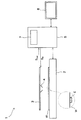
図1は、本実施形態に係る半導体試験装置の構成図である。
(1) First Embodiment FIG. 1 is a configuration diagram of a semiconductor test apparatus according to this embodiment.
この半導体試験装置1は、半導体ウエハWが載置されて水平方向に移動可能なステージ2と、半導体ウエハWに対向したプローブカード3と、パーソナルコンピュータ等の計算部5とを有する。
The
このうち、プローブカード3には、半導体ウエハWの端子Eに対応して複数のプローブ4が設けられており、試験に際してはそのプローブ4から試験信号Sinが端子Eに入力される。
Of these, the
また、ステージ2には不図示のヒータが内蔵されており、計算部5の制御によって半導体ウエハWを所望の試験温度に加熱することができる。
Further, a heater (not shown) is incorporated in the
そして、水平面内でのステージ2の移動量等や試験信号Sin等は計算部5により制御される。試験信号Sinの入力により半導体ウエハWから出力される出力信号Soutは計算部5に入力され、その出力信号Soutに基づいて計算部5が半導体ウエハWに形成されたチップの良否判定を行う。
The moving amount of the
計算部5は、記憶部7を有しており、良否判定の結果が試験結果データとしてその記憶部7に格納される。
The
試験結果データは、半導体ウエハWにおける不良チップの位置と、後述する不良のモードとを含み、ウエハマップの形でCRT等の表示部8に表示される。
The test result data includes the position of the defective chip on the semiconductor wafer W and a defect mode described later, and is displayed on the
次に、この半導体試験装置1を用いた半導体装置の製造方法について説明する。
Next, a method for manufacturing a semiconductor device using the
図2は、本実施形態に係る半導体装置の製造方法について示すフローチャートである。 FIG. 2 is a flowchart showing the method for manufacturing the semiconductor device according to this embodiment.
なお、特に断らない限り、このフローチャートは計算部5が実行するものである。
Unless otherwise specified, this flowchart is executed by the
最初のステップS1では、ステージ2により半導体ウエハWを90℃程度に加熱し、試験中に半導体チップに熱負荷を加えるようにする。
In the first step S1, the semiconductor wafer W is heated to about 90 ° C. by the
次に、ステップS2に移り、プローブ4と端子Eとが正しく導通しているかどうかの確認を行う。
Next, the process proceeds to step S2, and it is confirmed whether or not the
そして、ステップS3に移り、複数の端子E同士が電気的にショートしていないかどうかの確認を行う。 Then, the process proceeds to step S3 to check whether or not the plurality of terminals E are electrically short-circuited.
これらステップS2、S3は、試験前の基礎的な確認事項であって、これらの確認をした後に次のようにして実体的な試験が行われる。 These steps S2 and S3 are basic confirmation items before the test. After these confirmations, a substantial test is performed as follows.
まず、ステップS4では、チップに形成された回路のマージン測定を行う。 First, in step S4, the margin of the circuit formed on the chip is measured.
マージン測定とは、チップの入出力信号の変動が許容範囲内にあるかどうかを測定することをいう。 Margin measurement refers to measuring whether or not fluctuations in input / output signals of a chip are within an allowable range.
そして、入出力信号が許容範囲内にない場合にはそのチップを不良と判定し、そうでない場合には良品と判定する。 If the input / output signal is not within the allowable range, the chip is determined to be defective, and if not, the chip is determined to be non-defective.
測定の対象となる回路のマージンとしては種々あるが、そのうちの幾つかを図3に示す。 There are various margins of the circuit to be measured, some of which are shown in FIG.
また、図3に示す以外にも、動作電圧や動作電流等の動作パラメータを様々に振ることにより、チップが正常に動作することが可能な動作パラメータの範囲を探ることともマージン測定に含まれる。この場合、その範囲が、製品が保証する保証範囲よりも狭い場合にはそのチップを不良と判定し、そうでない場合には良品と判定する。例えば、電源電圧の保証範囲が2.7〜3.3Vであるときに、チップが正常に動作することが可能な電源電圧の範囲が2.9〜3.1Vである場合、そのチップは不良と判定される。 In addition to the one shown in FIG. 3, the margin measurement also includes searching for a range of operating parameters in which the chip can operate normally by varying operating parameters such as operating voltage and operating current. In this case, if the range is narrower than the guaranteed range guaranteed by the product, the chip is determined to be defective, and if not, it is determined to be a non-defective product. For example, when the guaranteed range of power supply voltage is 2.7 to 3.3 V and the power supply voltage range in which the chip can operate normally is 2.9 to 3.1 V, the chip is defective. It is determined.
このような回路のマージンの広狭は、ゲート電極等のデバイスパターンの幅の広狭に依存する。デバイスパターンの幅は、ウエハ面内でのエッチング速度等のプロセスパラメータに依存するものであって、そのプロセスパラメータはウエハ面内において連続的に変動し、あるチップにおいてのみ特異な値を取ることは稀である。従って、あるチップでマージンが狭いと判定された場合には、そのチップに隣接するチップでもマージンが狭いと判定される傾向が強い。 The width of the circuit margin depends on the width of the device pattern such as the gate electrode. The width of the device pattern depends on process parameters such as the etching rate in the wafer surface, and the process parameter continuously varies in the wafer surface, and it takes a unique value only in a certain chip. It is rare. Therefore, when it is determined that a margin is narrow in a certain chip, there is a strong tendency that a chip adjacent to the chip is also determined to have a narrow margin.
本実施形態では、図3の回路マージンの試験項目いずれかで不良と判定されたものを「マージン系の不良」と呼ぶ。 In this embodiment, what is determined to be defective in any of the circuit margin test items in FIG. 3 is referred to as “margin defect”.
また、チップが正常に動作することが可能な動作電圧や動作電流等の動作パラメータの範囲を探った結果、その範囲が製品の保証範囲よりも狭いことが明らかになった場合も、そのチップは「マージン系の不良」と判定される。 In addition, even if the result of exploring the range of operating parameters such as operating voltage and operating current that allow the chip to operate normally reveals that the range is narrower than the guaranteed range of the product, the chip It is determined as “margin defect”.
次に、ステップS5に移り、半導体チップに対して機能試験を行う。 Next, it moves to step S5 and performs a function test with respect to a semiconductor chip.
この機能試験では、半導体チップに電源電圧を供給し、そのチップ内の回路が行った論理演算によって出力端子から出力されるHIGHレベル電圧若しくはLOWレベル電圧等の出力電圧を測定する。そして、その出力電圧のレベルが所定の値になっている場合には、とのチップを良品と判定し、そうでない場合には不良と判定する。 In this functional test, a power supply voltage is supplied to a semiconductor chip, and an output voltage such as a HIGH level voltage or a LOW level voltage output from an output terminal by a logical operation performed by a circuit in the chip is measured. If the level of the output voltage is a predetermined value, the chip is determined to be non-defective, and if not, it is determined to be defective.
機能試験における試験結果は、製造途中でチップにたまたま付着したパーティクル等の異物に依存し、デバイスパターンの形状にはあまり依存しない。したがって、あるチップが機能試験において不良となっても、その隣のチップでは機能試験で不良になることは稀である。以下では、異物の付着により機能試験において不良となるものを「突発系の不良」と呼ぶことにする。 The test result in the functional test depends on foreign matters such as particles that happen to adhere to the chip during the manufacturing, and does not depend much on the shape of the device pattern. Therefore, even if a certain chip fails in the functional test, it is rare that the adjacent chip becomes defective in the functional test. In the following, what becomes defective in the functional test due to the adhesion of foreign matter will be referred to as “sudden failure”.
次いで、ステップS6に移り、試験対象の半導体チップについての合否判断を行う。この判断は、ステップS4とステップS5のいずれかで不良と判定されたチップを不合格とし、これらのステップS4、S5の両方で良品と判定されたものを合格とすることで行われる。 Next, the process proceeds to step S6, and a pass / fail judgment is made for the semiconductor chip to be tested. This determination is made by rejecting a chip determined to be defective in either step S4 or step S5 and accepting a chip determined to be non-defective in both steps S4 and S5.
続いて、ステップS7に移行し、ステップS6の合否判断の結果をウエハマップの形で表示する。 Subsequently, the process proceeds to step S7, and the result of the pass / fail judgment in step S6 is displayed in the form of a wafer map.
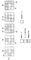
図4は、そのウエハマップの一例を示す図である。 FIG. 4 is a diagram showing an example of the wafer map.
ウエハマップでは、良品チップと不良チップとが色の濃淡で区別して表示される。なお、図4では、色の濃淡をハッチングによって示している。 In the wafer map, non-defective chips and defective chips are displayed with different shades of color. In FIG. 4, shades of color are indicated by hatching.
次に、ステップS8に移り、不良チップと判定されたチップをマージン系の不良と突発系の不良とに分類し、それらをウエハマップ上で別々の色により再表示する。このような不良の分類は、不良チップがステップS4のマージン測定とステップS5の機能試験のどちらで不良になったかに基づいて、計算部5が自動で行う。
Next, the process proceeds to step S8, and the chips determined as defective chips are classified into marginal defects and sudden defects, and these are redisplayed in different colors on the wafer map. Such a failure classification is automatically performed by the
図5は、試験対象の5個の良品チップ20を中心にしたこのウエハマップの拡大図である。但し、図5と後述の図6及び図7では、色の違いをハッチングで表している。
FIG. 5 is an enlarged view of this wafer map centering on the five
このように色分け表示をすることで、マージン系の不良チップ22と突発系の不良チップ23の面内分布を把握することができる。
By performing color-coded display in this way, the in-plane distribution of the marginal
なお、色分けに代えて、アルファベットや数字等の記号によりマージン系の不良チップ22と突発系の不良チップとを表示するようにしてもよい。
Instead of color coding, the margin
次に、ステップS9に移り、良品チップ20の周囲に存在するマージン系の不良チップ22の分布を調査する。
Next, the process proceeds to step S9, and the distribution of the margin
本実施形態では、対象の良品チップ20と隣接して存在するマージン系の不良チップ22の個数が所定個数以上かどうか、例えば2個以上かどうかを調査する。
In the present embodiment, it is investigated whether or not the number of margin
なお、良品チップ20に隣接するチップとは、該チップ20の四辺に隣接する四個のチップと、該チップ20の対角線方向に隣接する四個のチップの計八個のチップである。
The chips adjacent to the
既述のように、あるチップで回路マージンが狭い場合には、そのチップに隣接するチップでも回路マージンが狭くなる傾向がある。したがって、良品チップ20の周囲に所定個数(この例では2個)以上のマージン系の不良チップ22が存在する場合には、その不良チップ22に隣接する良品チップ20も回路マージンが狭く、良品チップ20が潜在的に不良になる可能性が高い。
As described above, when a circuit margin is narrow in a certain chip, the circuit margin tends to be narrow in a chip adjacent to the chip. Therefore, when there are a predetermined number (two in this example) of marginal
そこで、次のステップS10では、良品チップ20に隣接するマージン系の不良チップ22の個数が所定個数以上の場合に、その良品チップ20を潜在的に不良になる可能性が高い準良品チップ(第1タイプの良品チップ)と判定する。
Therefore, in the next step S10, when the number of margin
一方、良品チップ20に隣接するマージン系の不良チップ22の個数が所定個数未満の場合には、その良品チップを潜在的に不良になる可能性が低い真の良品チップ(第2タイプの良品チップ)と判定する。
On the other hand, when the number of margin
そして、本ステップにより準良品チップである(YES)と判定された場合にはステップS11に移り、半導体試験装置1が備える記憶部7にその良品チップ20の種別を準良品として記憶させる。
If it is determined that the chip is a semi-defective chip (YES) in this step, the process proceeds to step S11, and the type of the
一方、ステップS10において準良品チップではなく(NO)、真の良品チップであると判定された場合には、ステップS12に移り、上記の記憶部7に良品チップ20の種別を真の良品として記憶させる。
On the other hand, if it is determined in step S10 that the chip is not a semi-defective chip (NO) but a true good chip, the process proceeds to step S12, and the type of the
そして、半導体試験装置の表示部8には、図6に示すように、準良品と判断された良品チップ20が他のチップとは異なる色で表示される。
As shown in FIG. 6, the
なお、このように色で表示するのではなく、アルファベットや数字等の記号によって準良品のチップ20を表示するようにしてもよい。
Instead of displaying in color in this way, the
図6は、図5と同一の5個の良品チップ20を中心にしたウエハマップの拡大図である。この例では、右から2番目と3番目の良品チップ20が、2個以上のマージン系の不良チップと隣接しているので、他の良品チップとは異なる色で表示されている。
FIG. 6 is an enlarged view of a wafer map centering on the five
続いて、ステップS13に移り、計算部5が記憶部7を参照し、良品チップ20の種別が準良品かどうかを判断する。
Subsequently, the process proceeds to step S13, where the
そして、準良品である(YES)と判断された場合には、ステップS14に移り、準良品と判定された良品チップ20に対してステップS4におけるよりも合格条件を厳しくしたマージン系の追加試験を行う。
If it is determined that the product is a semi-defective product (YES), the process proceeds to step S14, and a margin-type additional test with a more strict pass condition than that in step S4 is performed on the
この場合の追加試験の項目としては、図3に示した試験がある。そして、合格条件を厳しくするには、図3に示されるマージンの幅を、ステップS4におけるよりも狭くすればよい。 As an additional test item in this case, there is a test shown in FIG. Then, in order to make the pass condition stricter, the margin width shown in FIG. 3 may be made narrower than in step S4.
なお、マージンの幅をあまり狭くし過ぎると、殆ど全ての良品チップ20が不良になるおそれがある。したがって、追加試験では、ステップS4におけるマージンから5%以内の範囲でマージンを狭くするのが好ましい。
If the margin width is too narrow, almost all
また、動作電圧や動作電流等の動作パラメータの保証範囲をステップS4におけるよりも広くすることで、この追加試験の合格条件を厳しくしてもよい。この場合、広げられた保証範囲でチップが動作する場合には合格となり、そうでない場合には不合格となる。 Further, the pass condition of this additional test may be made stricter by making the guaranteed range of the operating parameters such as the operating voltage and the operating current wider than in step S4. In this case, if the chip operates within the extended warranty range, it will be accepted, otherwise it will be rejected.
例えば、ステップS4における電源電圧の保証範囲が2.7〜3.3Vであるとき、保証範囲をさらに2.6〜3.4Vに広げ、この範囲で動作すればそのチップは合格となる。 For example, when the guaranteed range of the power supply voltage in step S4 is 2.7 to 3.3 V, the guaranteed range is further expanded to 2.6 to 3.4 V, and the chip passes if it operates in this range.
或いは、試験温度をステップS4よりも高い温度してもよい。このようにすると、準良品と判定されたチップに印加される熱負荷がステップS4よりも大きくなるので、ステップS4で合格になったものが不合格と判断され易くなり、ステップS4におけるよりも合格条件を厳しくすることができる。 Alternatively, the test temperature may be higher than that in step S4. In this way, since the thermal load applied to the chip determined to be a non-defective product is greater than that in step S4, it is easier to determine that what has passed in step S4 is rejected, which is more than that in step S4. Conditions can be tightened.
この場合、ステップS4と比較して温度上昇が僅かだと、チップに印加される熱負荷が不十分となり、合格条件があまり厳しくならない場合がある。したがって、ステップS4の温度と比較して3%以上温度を高くし、チップに十分に熱負荷を加えるのが好ましい。 In this case, if the temperature rise is small compared to step S4, the thermal load applied to the chip becomes insufficient, and the pass condition may not be so strict. Therefore, it is preferable to increase the temperature by 3% or more as compared with the temperature in step S4 and apply a sufficient heat load to the chip.
準良品と判断されていた良品チップ20は、このようにステップS4よりも厳しい合格条件で合格となった場合には、市場に出してもマージン系の不良が発生し難いと考えられ、真の良品チップとして扱ってもよい。
If the
そこで、次のステップS15では、準良品と判定された良品チップ20が追加試験において合格かどうかを判断し、合格(YES)と判断された場合には、ステップS17においてその良品チップ20を真の良品チップとして出荷する。
Therefore, in the next step S15, it is determined whether or not the
なお、既述のステップS13において準良品チップでない(NO)と判断されている場合には、このステップS15において自動的に合格(YES)と判断し、ステップS17に移行する。 If it is determined in step S13 that the chip is not a near-defective chip (NO), it is automatically determined in step S15 that the chip has passed (YES), and the process proceeds to step S17.
一方、ステップS15において合格でない(NO)と判断された場合には、ステップS16において良品チップ20を不良品として取り扱う。そして、このように不良品と扱われる良品チップ20にはインクでマーキングが施され、良品と誤認されないようにする。なお、インクによるマーキングに代えて、半導体試験装置1がウエハマップの形で保持する試験結果データに、良品チップ20を不良品として取り扱うべき旨のデータを付加し、ウエハマップ上でそのチップを他のチップと異なる色で表示するようにしてもよい。このような処理はデータマーキング処理とも呼ばれる。
On the other hand, if it is determined in step S15 that it is not acceptable (NO), the
そして、半導体試験装置の表示部8には、図7に示すように、不良品として取り扱うべき良品チップ20が他のチップとは異なる色で表示される。なお、このように色で表示するのではなく、アルファベットや数字等の記号で表示するようにしてもよい。
As shown in FIG. 7, the
図7は、図5と同一の5個の良品チップ20を中心にしたウエハマップの拡大図である。この例では、右から3番目の準良品と判定されたチップ20が、上記の追加試験で不合格となったため、データマーキング処理によって他のチップと異なる色で表示されている。
FIG. 7 is an enlarged view of the wafer map centering on the five
以上により、本実施形態に係る半導体装置の製造工程の主要工程を終了する。 Thus, the main process of the semiconductor device manufacturing process according to this embodiment is completed.
上記した本実施形態によれば、図5に示したように、良品チップ20の周りの不良チップをマージン系の不良チップ22と突発系の不良チップ23とに分類する。そして、図6に示したように、良品チップ20に隣接するマージン系の不良チップ22の個数が所定個数以上の場合に、その良品チップ20を準良品チップと判定する。
According to the above-described embodiment, as shown in FIG. 5, the defective chips around the
潜在的に不良になる可能性のある準良品チップをこのように認識しておくことで、準良品チップを後工程や市場に出すのを留保でき、後工程や市場に出てから不良になるチップの数を低減することができる。 By recognizing semi-good chips that can potentially be defective in this way, it is possible to reserve that semi-defective chips are put on the post-process or market, and become defective after they are put on the post-process or market. The number of chips can be reduced.
しかも、準良品であるかどうかの判定は、計算部5が自動で行うので、その判定に作業者の個人差が入り込む余地がないうえ、極めて短時間に判定を行うことができ、半導体装置の出荷を遅滞なく進めることができる。
Moreover, since the
更に、図7に示したように、準良品と判定された良品チップ20に対し、ステップS4におけるよりも合格条件が厳しいマージン系の追加試験を行い、この試験で不合格となったものを不良品として扱うと共に、合格となったものを真の良品チップとして扱う。
Further, as shown in FIG. 7, a margin-type additional test with stricter pass conditions than in step S4 is performed on the
これにより、潜在的に不良になるチップを不良品として選別し、真の良品チップのみを後工程や市場に出すことができ、不良になる可能性のあるチップを後工程等に出す危険性を更に低減できる。 As a result, chips that are potentially defective can be selected as defective products, and only genuine good chips can be put on the post-process or market, and there is a risk that a chip that may become defective can be put on the post-process etc. Further reduction can be achieved.
ところで、一般的には、ある半導体ウエハにおいて不良チップが多数存在する場合には、ウエハ中に良品チップが存在したとしても、その良品チップが後工程等において不良になる危険性があるため、その半導体ウエハは廃棄処分するのが普通である。 By the way, in general, when there are many defective chips in a certain semiconductor wafer, even if there are good chips in the wafer, there is a risk that the good chips may become defective in subsequent processes. Semiconductor wafers are usually discarded.
このような半導体ウエハに対し、本実施形態を適用すると、廃棄処分をせずにその中から潜在的に不良になる可能性の低い良品チップを取り出すことができる。これについて以下に説明する。 When this embodiment is applied to such a semiconductor wafer, it is possible to take out non-defective chips that are unlikely to become potentially defective without being disposed of. This will be described below.
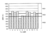
図8は、ある品種における半導体ウエハWの歩留まりを示すグラフである。このグラフの横軸は半導体ウエハWの番号を示し、縦軸はその半導体ウエハにおける良品チップの歩留まりを示す。 FIG. 8 is a graph showing the yield of the semiconductor wafer W in a certain product type. The horizontal axis of this graph indicates the number of the semiconductor wafer W, and the vertical axis indicates the yield of non-defective chips on the semiconductor wafer.
これに示されるように、同じ品種であっても、半導体ウエハWによって歩留まりにはばらつきがある。 As shown in this figure, the yield varies depending on the semiconductor wafer W even in the same type.
この例では、歩留まりの高低を示す指標として、ウエハグレードWG1〜WG3を用いている。 In this example, wafer grades WG1 to WG3 are used as indices indicating the level of yield.
全ウエハの歩留まりの標準偏差をσとする場合、ウエハグレードWG1のウエハは、その歩留まりが、全ウエハの平均歩留まりYと2σとの和(Y+2σ)よりも高いウエハとして定義される。 When the standard deviation of the yield of all wafers is σ, a wafer of the wafer grade WG1 is defined as a wafer whose yield is higher than the sum of the average yields Y and 2σ of all wafers (Y + 2σ).
また、ウエハグレードWG2のウエハは、その歩留まりが、全ウエハの平均歩留まりYと2σとの差(Y−2σ)よりも高く、且つY+2σよりも低いウエハとして定義される。 A wafer of wafer grade WG2 is defined as a wafer whose yield is higher than the difference between the average yield Y of all wafers and 2σ (Y−2σ) and lower than Y + 2σ.
そして、ウエハグレードWG3のウエハは、その歩留まりが、全ウエハの平均歩留まりYと2σとの差(Y−2σ)よりも低いウエハとして定義される。 A wafer of wafer grade WG3 is defined as a wafer whose yield is lower than the difference between the average yield Y of all wafers and 2σ (Y−2σ).
図9は、ウエハグレードWG2の不良チップの分布を示すウエハマップである。また、図10は、ウエハグレードWG3の不良チップの分布を示すウエハマップである。これらの図に示されるように、不良チップが多数存在するウエハでは、その中にたとえ良品チップが存在しても、それが本当に良品チップかどうか疑わしい。 FIG. 9 is a wafer map showing the distribution of defective chips of wafer grade WG2. FIG. 10 is a wafer map showing the distribution of defective chips of wafer grade WG3. As shown in these drawings, in a wafer in which many defective chips exist, even if there are good chips, it is doubtful whether or not they are really good chips.
図11は、図10に示したウエハグレードWG3のウエハに対し、本実施形態を適用して準良品チップに対して追加試験(ステップS14)を行い、その準良品チップの中で不良チップと再判定されたチップの分布を示すウエハマップである。 FIG. 11 shows the wafer grade WG3 wafer shown in FIG. 10 is subjected to an additional test (step S14) on the semi-defective chip by applying this embodiment. It is a wafer map which shows distribution of the determined chip | tip.
これに示すように、本実施形態の追加試験(ステップS14)を行うことで、元々は良品と判断されていたチップの中に不良と再判定されるものがある。その不良チップは、良品と判断されたものの潜在的に不良になる可能性が高いものである。したがって、このような不良チップを除けば、残りの良品チップは市場等において不良になる可能性が低く、半導体ウエハを廃棄せずに良品チップを取り出すことができるようになる。 As shown in this, by performing the additional test (step S14) of this embodiment, some chips that were originally determined to be non-defective are re-determined as defective. Although the defective chip is determined to be a non-defective product, there is a high possibility that the defective chip is potentially defective. Therefore, except for such defective chips, the remaining good chips are unlikely to become defective in the market or the like, and the good chips can be taken out without discarding the semiconductor wafer.
このように、本実施形態を適用することでウエハから後発的に不良になる可能性の低い良品チップを取り出すことができ、ウエハを廃棄処分する必要がなく、コスト効率が高くなる。 As described above, by applying the present embodiment, it is possible to take out non-defective chips that are unlikely to be defective later from the wafer, and it is not necessary to dispose of the wafer, thereby increasing cost efficiency.
(2)第2実施形態
本実施形態は、第1実施形態と比較してステップS9とステップS10の処理内容が異なる。
(2) Second Embodiment The present embodiment is different from the first embodiment in the processing contents of step S9 and step S10.
図12及び図13は、本実施形態におけるステップS9とステップS10の処理内容を説明するための模式図である。 12 and 13 are schematic diagrams for explaining the processing contents of steps S9 and S10 in the present embodiment.
本実施形態では、図12に示すように、良品チップ20に隣接するチップ27に予め係数を付与しておく。
In the present embodiment, as shown in FIG. 12, a coefficient is given in advance to the
係数の付与の仕方は特に限定されない。但し、良品チップ20の四辺に隣接するチップ27については、良品チップ20の対角線方向に隣接するチップ27よりも良品チップ20の良・不良に与える影響が大きいため、図示のように対角線方向に隣接するチップ27よりも高い値であるのが好ましい。
There is no particular limitation on the method of applying the coefficient. However, since the
図14に、係数の付与の仕方の別の例を示す。 FIG. 14 shows another example of how to assign coefficients.
そして、第1実施形態のステップS8で説明したように、チップ27のうち不良チップと判定されたものをマージン系の不良と突発系の不良とに分類し、それらをウエハマップ上で図13のように色分けして表示する。
Then, as described in step S8 of the first embodiment, among the
なお、図13では、図を見易くするためにマージン系の不良のみを示している。また、このような色分けに代えて、アルファベットや数字等の記号によってマージン系と突発系の不良とを分けて表示してもよい。 In FIG. 13, only margin-related defects are shown in order to make the drawing easier to see. Further, instead of such color coding, marginal and sudden failure may be displayed separately by symbols such as alphabets and numerals.
そして、ステップS9におけるマージン系の不良チップの分布の調査では、良品チップ20に隣接するチップ27のうち、マージン系の不良チップであるものの係数の総和Sを求め、該総和が所定値D1以上かどうかを調査する。
Then, in the investigation of the distribution of margin defective chips in step S9, the sum S of coefficients of the
所定値D1を3とした場合、図13の例では、総和Sが3.5(=1.0+1.0+1.0+0.5)であるため、総和Sは所定値D1以上となる。 When the predetermined value D 1 is 3, in the example of FIG. 13, the total sum S is 3.5 (= 1.0 + 1.0 + 1.0 + 0.5), so the total sum S is equal to or greater than the predetermined value D 1 .
その後、ステップS10において、総和Sが所定値D1以上の場合に良品チップ20を準良品と判定し、総和Sが所定値D1未満の場合に良品チップ20を真の良品チップと判定する。
Determining Thereafter, in step S10, the total sum S is a
この例では、総和S(=3.5)が所定値D1(=3)以上なので、良品チップ20は準良品と判定される。
In this example, since the sum S (= 3.5) is equal to or greater than the predetermined value D 1 (= 3), the
これ以降のステップは第1実施形態と同様である。 The subsequent steps are the same as in the first embodiment.
以上説明した本実施形態によれば、良品チップ20に隣接するチップ27に予め係数を付与しておく。そのチップ27のうちマージン系の不良チップの係数の総和Sが所定値D1以上の場合には、良品チップ20の周囲に多数のマージン系の不良チップが存在することになり、良品チップ20が潜在的に不良になる可能性がある。よって、その場合には良品チップ20を準良品として扱うことで、良品チップ20を市場等に出すのを留保でき、市場において後発的に不良となるチップの数を低減できる。
According to the present embodiment described above, a coefficient is given in advance to the
なお、図12に示したチップへの係数の付与については、マージン系の不良を更に複数のカテゴリに分け、そのカテゴリに応じて係数の値を変えるようにしてもよい。この場合のカテゴリとしては、図3に示した試験項目がある。 In addition, regarding the assignment of coefficients to the chip shown in FIG. 12, margin-related defects may be further divided into a plurality of categories, and the coefficient values may be changed according to the categories. The category in this case includes the test items shown in FIG.
図3の試験項目のうち、電源端子を試験対象とするものは、それ以外の端子を対象とするものと比較して、不良となった場合に隣接するチップを潜在的に不良にする可能性が高い。 Among the test items shown in FIG. 3, the test target for the power supply terminal may potentially make the adjacent chip defective if it becomes defective compared to the test for other terminals. Is expensive.
したがって、電源端子を試験対象とする試験項目で不良となったマージン系の不良チップについては、電源端子以外の端子を試験対象とする試験項目で不良となったものよりも係数を高くするのが好ましい。このように試験項目毎に係数を変えることにより、マージン系の不良チップが隣接する良品チップに与える影響を、試験項目を加味しながら判断することができ、良品チップが準良品チップであるかどうかの判断をより正確に行うことができる。 Therefore, for margin-type defective chips that have failed in test items that have power supply terminals as test targets, the coefficient should be higher than those that have failed in test items that have terminals other than power supply terminals as test targets. preferable. In this way, by changing the coefficient for each test item, it is possible to determine the effect of a marginal defective chip on the adjacent non-defective chip, taking into account the test item, and whether or not the non-defective chip is a semi-defective chip. Can be determined more accurately.
(3)第3実施形態
本実施形態では、第2実施形態で説明したチップの係数(図12)を利用して、次のようにステップS9とステップS10を行う。
(3) Third Embodiment In the present embodiment, Step S9 and Step S10 are performed as follows using the coefficient of the chip described in the second embodiment (FIG. 12).
図15は、本実施形態におけるステップS9とステップS10の処理内容を説明するための模式図である。 FIG. 15 is a schematic diagram for explaining the processing contents of steps S9 and S10 in the present embodiment.
本実施形態では、ステップS9において、良品チップ20に隣接するチップ27のうち、マージン系の不良であるものの中心同士を線分で結び、良品チップ20を横切る線分の数と重み係数Fとの積Pを求める。重み係数Fは特に限定されないが、本実施形態では例えば0.2とする。
In this embodiment, in step S9, among the
更に、良品チップ20に隣接するチップ27のうち、マージン系の不良であるものの係数の総和Sを求め、その総和Sと上記の積Pとの和が所定値D2以上かどうかを調査する。
Furthermore, among the
図示の例では、良品チップを横切る線分の数が2であるから、重み係数Fとその線分の数との積Pは0.4(=2×0.2)である。また、上記の総和Sは3.5(=1.0+1.0+1.0+0.5)であるから、総和Sと積Pとの和は3.9となる。 In the illustrated example, since the number of line segments crossing the non-defective chip is 2, the product P of the weighting factor F and the number of the line segments is 0.4 (= 2 × 0.2). Further, since the total sum S is 3.5 (= 1.0 + 1.0 + 1.0 + 0.5), the sum of the total sum S and the product P is 3.9.
また、所定値D2は、第2実施形態における所定値D1と同一であっても異なってもよいが、本実施形態では例えば3とする。その場合、総和Sと積Pとの和(=3.9)は、所定値D2(=3)以上ということになる。 The predetermined value D 2 may be the same or different and the predetermined value D 1 of the second embodiment, but in this embodiment a 3, for example. In this case, the sum (= 3.9) of the sum S and the product P is equal to or greater than a predetermined value D 2 (= 3).
その後、ステップS10において、総和Sと積Pとの和が所定値D2以上の場合に良品チップ20を準良品と判定し、総和Sと積Pとの和が所定値D2未満の場合に良品チップ20を真の良品チップと判定する。
Thereafter, in step S10, the
この例では、上記のように総和Sと積Pとの和(=3.9)が所定値D2(=3)以上なので、良品チップ20は準良品と判定される。
In this example, since the sum (= 3.9) of the sum S and the product P (= 3.9) is equal to or greater than the predetermined value D 2 (= 3) as described above, the
これ以降のステップは第1実施形態と同様である。 The subsequent steps are the same as in the first embodiment.
以上説明した本実施形態によれば、図15に示したように、マージン系の不良チップの中心同士を線分で結ぶ。このとき、良品チップ20を横切る線分の数が多いほど、良品チップ20は、その電気的特性が周囲のマージン系の不良チップと同様の傾向を呈すると予測されるので、潜在的な不良チップであると推測できる。
According to the present embodiment described above, the centers of marginal defective chips are connected by line segments as shown in FIG. At this time, as the number of line segments crossing the
よって、このように良品チップ20を横切る線分の数を加味することにより、良品チップ20が準良品であるかどうかの判断を行うことができる。そして、準良品であると判断された良品チップ20については、市場等に出すのを留保でき、市場等において後発的に不良となるチップの数を低減できる。
Therefore, it is possible to determine whether or not the
(4)第4実施形態
本実施形態では、第1〜第3実施形態と比較して、ステップS15以降の工程のみが異なる。
(4) 4th Embodiment In this embodiment, compared with 1st-3rd Embodiment, only the process after step S15 differs.
図16は、本実施形態に係る半導体装置の製造方法について示すフローチャートである。 FIG. 16 is a flowchart showing the method for manufacturing the semiconductor device according to this embodiment.
本実施形態では、図16に示すように、ステップS15において良品チップが追加試験で合格でない(NO)と判断された場合、ステップS20に移る。 In this embodiment, as shown in FIG. 16, when it is determined in step S15 that the non-defective chip is not passed in the additional test (NO), the process proceeds to step S20.
そのステップS20では、チップに要求される品質が、ハイグレード(第1の品質)かそれよりも低いローグレード(第2の品質)のどちらであるかの判断を行う。 In step S20, it is determined whether the quality required for the chip is high grade (first quality) or lower grade (second quality) lower than that.
ここで、ハイグレードのチップは、例えば車載用等の人命に関わる機器に使用されるものである。一方、ローグレードのチップは、音響機器や玩具等のように、故障しても人命に影響の出ないものである。 Here, the high-grade chip is used for a device related to human life such as in-vehicle use. On the other hand, low-grade chips, such as audio equipment and toys, do not affect human life even if they break down.
追加試験で合格でないと判断されたチップにハイグレードな品質が要求されている場合、そのチップを市場に出したのでは後発的にそのチップが不良になり、重大な事故を起こす危険がある。 If a high-grade quality is required for a chip that is determined not to pass the additional test, there is a risk that if the chip is put on the market, the chip will become defective later and cause a serious accident.
そこで、ステップS20においてハイグレードであると判断された場合には、そのチップを市場に出さずに廃棄処分する。 Therefore, if it is determined in step S20 that it is a high grade, the chip is discarded without being put on the market.
一方、ステップS20においてローグレードであると判断された場合は、チップが後発的に不良となっても重大な事故を起こす危険性が低いので、ローグレード品としてそのチップを出荷する。 On the other hand, if it is determined that the grade is low grade in step S20, the risk of causing a serious accident is low even if the chip becomes defective later, so the chip is shipped as a low grade product.
以上により、本実施形態に係る半導体装置の基本ステップを終了する。 Thus, the basic steps of the semiconductor device according to this embodiment are completed.
上記した本実施形態によれば、追加試験で合格でないと判断されたチップについて、ステップS20においてハイグレードかローグレードかを判断する。そして、ハイグレードと判断された場合にはステップS22でそのチップを廃棄するので、そのチップが市場に出回って重大な事故を起こす危険性を低減できる。また、ローグレードと判断された場合には、ステップS21でローグレード品として出荷するので、追加試験で合格でないと判断されたチップを有効活用することができる。 According to the above-described embodiment, for a chip that is determined not to pass in the additional test, it is determined in step S20 whether it is a high grade or a low grade. When the high grade is determined, the chip is discarded in step S22, so that the risk that the chip will be on the market and cause a serious accident can be reduced. If it is determined that the grade is low grade, the product is shipped as a low grade product in step S21. Therefore, it is possible to effectively use the chip that is judged not to pass the additional test.
以下に、本発明の特徴を付記する。 The features of the present invention are added below.
(付記1) 所定の試験に基づいて不良と判断された半導体ウエハ上の不良チップを第1の不良モードと第2の不良モードとに分類し、
前記所定の試験に基づいて良品と判断された前記半導体ウエハ上の良品チップの周囲に存在する前記第1の不良モードに属する不良チップの分布を調査し、
前記分布に基づいて、前記良品チップを第1タイプの良品チップとするか第2タイプの良品チップとするかの判定を行うこと
を特徴とする半導体装置の製造方法。
(Appendix 1) Classifying defective chips on a semiconductor wafer determined to be defective based on a predetermined test into a first defect mode and a second defect mode;
Investigating the distribution of defective chips belonging to the first defective mode existing around non-defective chips on the semiconductor wafer determined to be non-defective based on the predetermined test;
Based on the distribution, it is determined whether the non-defective chip is a first-type non-defective chip or a second-type non-defective chip.
(付記2) 前記調査において、前記良品チップと隣接して存在する前記第1の不良モードの前記不良チップの個数が所定個数以上かどうかを調査し、
前記判定において、前記不良チップの前記個数が前記所定個数以上の場合に前記良品チップを前記第1タイプの良品チップと判定し、前記不良チップの前記個数が前記所定個数未満の場合に前記良品チップを前記第2タイプの良品チップと判定することを特徴とする付記1に記載の半導体装置の製造方法。
(Supplementary Note 2) In the investigation, whether or not the number of the defective chips in the first defective mode existing adjacent to the non-defective chips is a predetermined number or more,
In the determination, when the number of the defective chips is equal to or greater than the predetermined number, the non-defective chip is determined as the first type non-defective chip, and when the number of the defective chips is less than the predetermined number, the
(付記3) 前記良品チップに隣接するチップに予め係数を付与し、
前記調査において、前記良品チップに隣接するチップのうち、前記第1の不良モードに属する不良チップの前記係数の総和を求め、該総和が所定値以上かどうかを調査し、
前記判定において、前記総和が前記所定値以上の場合に前記良品チップを前記第1タイプの良品チップと判定し、前記総和が前記所定値未満の場合に前記良品チップを第2タイプの良品チップと判定することを特徴とする付記1に記載の半導体装置の製造方法。
(Supplementary Note 3) A coefficient is given in advance to a chip adjacent to the non-defective chip,
In the investigation, a total of the coefficients of defective chips belonging to the first defective mode among chips adjacent to the non-defective chip is obtained, and whether the total is equal to or greater than a predetermined value is investigated.
In the determination, when the total is equal to or greater than the predetermined value, the non-defective chips are determined as the first type non-defective chips, and when the total is less than the predetermined value, the non-defective chips are determined as the second type non-defective chips. The method of manufacturing a semiconductor device according to
(付記4) 前記調査において、前記良品チップに隣接するチップのうち、前記第1の不良モードに属する不良チップの中心同士を線分で結び、前記良品チップを横切る前記線分の数と重み係数との積を求め、該積と前記総和との和が前記所定値以上かどうかを調査し、
前記判定において、前記和が前記所定値以上の場合に前記良品チップを前記第1タイプの良品チップと判定し、前記和が前記所定値未満の場合に前記良品チップを第2タイプの良品チップと判定することを特徴とする付記3に記載の半導体装置の製造方法。
(Supplementary Note 4) In the investigation, among the chips adjacent to the non-defective chip, the centers of the defective chips belonging to the first defective mode are connected with line segments, and the number of the line segments crossing the non-defective chip and the weight coefficient , And investigate whether the sum of the product and the sum is greater than or equal to the predetermined value,
In the determination, when the sum is not less than the predetermined value, the non-defective chip is determined as the first type non-defective chip, and when the sum is less than the predetermined value, the non-defective chip is determined as the second type non-defective chip. The method of manufacturing a semiconductor device according to
(付記5) 前記不良チップを前記第1の不良モードと前記第2の不良モードとに分類するときに、前記第1の不良モードを更に複数のカテゴリに分け、
前記カテゴリに応じて、前記係数の値を変えることを特徴とする付記3に記載の半導体装置の製造方法。
(Supplementary Note 5) When the defective chip is classified into the first defective mode and the second defective mode, the first defective mode is further divided into a plurality of categories,
4. The method of manufacturing a semiconductor device according to
(付記6) 前記良品チップの四辺に隣接するチップの係数を、前記良品チップの対角線方向に隣接するチップの係数よりも高くすることを特徴とする付記3に記載の半導体装置の製造方法。
(Additional remark 6) The manufacturing method of the semiconductor device of
(付記7) 前記第1タイプと判定された前記良品チップに対し、前記所定の試験よりも合格条件が厳しい追加試験を行い、
前記追加試験で合格と判定された前記良品チップを真の良品チップと判定し、前記追加試験で不合格と判定された前記良品チップを不良チップと判定することを特徴とする付記1〜6のいずれかに記載の半導体装置の製造方法。
(Appendix 7) For the non-defective chip determined to be the first type, an additional test with a stricter pass condition than the predetermined test is performed,
(付記8) 前記追加試験において、前記所定の試験におけるよりも試験温度を高くすることにより、前記合格条件を厳しくすることを特徴とする付記7に記載の半導体装置の製造方法。
(Additional remark 8) In the said additional test, the said acceptance conditions are made severe by making test temperature higher than in the said predetermined test, The manufacturing method of the semiconductor device of
(付記9) 前記追加試験において、前記所定の試験におけるよりも、動作電圧又は動作電流の保証範囲を広くすることにより、前記合格条件を厳しくすることを特徴とする付記7に記載の半導体装置の製造方法。
(Additional remark 9) In the said additional test, the said pass conditions are made severe by widening the guarantee range of an operating voltage or an operating current rather than in the said predetermined test, The semiconductor device of
(付記10) 前記追加試験で不合格と判定された前記良品チップに要求される品質が、第1の品質とそれよりも低い第2の品質のどちらであるかの判断を行い、前記第1の品質であると判断された場合には前記不合格と判定された前記良品チップを廃棄処分し、前記第2の品質であると判断された場合には前記不合格と判定された前記良品チップを出荷することを特徴とする付記7〜付記9のいずれかに記載の半導体装置の製造方法。
(Additional remark 10) It is judged whether the quality requested | required of the said non-defective chip | tip determined to be unacceptable by the said additional test is 1st quality or 2nd quality lower than it. The non-defective chip determined to be rejected is determined to be discarded when it is determined to be of the quality, and the non-defective chip determined to be rejected when determined to be of the second quality. 10. The method for manufacturing a semiconductor device according to any one of
(付記11) 前記第1の不良モードには、
電源の電流測定、
電源の静止電流測定、
出力端子のHIGHレベル測定、
出力端子のLOWレベル測定、
入力端子のリーク電流測定、
入力端子からGND端子へのリーク電流測定、
電源端子から入力端子へのリーク電流測定、
BUS回路の入力端子及び出力端子のリーク電流測定、
被測定端子からGND端子へのリーク電流測定、及び
電源端子から被測定端子へのリーク電流測定
のいずれかの試験において不良チップと判断される不良チップが含まれること
を特徴とする付記1〜10のいずれかに記載の半導体装置の製造方法。
(Appendix 11) In the first failure mode,
Power supply current measurement,
Quiescent current measurement of power supply,
High level measurement of output terminal,
LOW level measurement of output terminal,
Input terminal leakage current measurement,
Leakage current measurement from input terminal to GND terminal,
Leakage current measurement from power supply terminal to input terminal,
Measurement of leakage current at the input and output terminals of the BUS circuit,
(付記12) 前記第2の不良モードには、異物の付着により不良チップと判断される不良チップが含まれること
を特徴とする付記1〜11のいずれかに記載の半導体装置の製造方法。
(Supplementary note 12) The method for manufacturing a semiconductor device according to any one of
(付記13) 半導体ウエハに形成された半導体チップに、所定の試験における試験信号を入力して、該半導体チップの合否判断を行う計算部を有し、
前記計算部が、
前記合否判断において不良と判断された不良チップを第1の不良モードと第2の不良モードとに分類し、
前記合否判断において良品と判断された良品チップの周囲に存在する前記第1の不良モードに属する不良チップの分布を調査し、
前記分布に基づいて、前記良品チップを第1タイプの良品チップとするか第2タイプの良品チップとするかの判定を行うこと
を特徴とする半導体試験装置。
(Additional remark 13) It has the calculation part which inputs the test signal in a predetermined | prescribed test to the semiconductor chip formed in the semiconductor wafer, and performs the pass / fail judgment of this semiconductor chip,
The calculation unit is
Classifying the defective chip determined to be defective in the pass / fail determination into a first defect mode and a second defect mode;
Investigate the distribution of defective chips belonging to the first defective mode existing around non-defective chips determined to be non-defective in the pass / fail determination,
Based on the distribution, it is determined whether the non-defective chip is a first-type non-defective chip or a second-type non-defective chip.
(付記14) 前記計算部は、
前記第1タイプと判定された前記良品チップに対し、前記所定の試験よりも合格条件が厳しい追加試験を行い、
前記追加試験で合格と判定された前記良品チップを真の良品チップと判定し、前記追加試験で不合格と判定された前記良品チップを不良チップと判定することを特徴とする付記13に記載の半導体試験装置。
(Supplementary Note 14) The calculation unit
For the non-defective chip determined to be the first type, an additional test with a stricter pass condition than the predetermined test is performed,
Item 14. The supplementary note 13, wherein the non-defective chip determined to be acceptable in the additional test is determined to be a true non-defective chip, and the non-defective chip determined to be unacceptable in the additional test is determined to be a defective chip. Semiconductor test equipment.
(付記15) 前記ステージは前記半導体ウエハを加熱する機能を有し、
前記計算部は、前記追加試験において、前記ステージを制御して前記所定の試験におけるよりも試験温度を高くすることにより、前記合格条件を厳しくすることを特徴とする付記14に記載の半導体試験装置。
(Supplementary Note 15) The stage has a function of heating the semiconductor wafer,
15. The semiconductor test apparatus according to appendix 14, wherein in the additional test, the pass condition is made stricter by controlling the stage to raise a test temperature higher than in the predetermined test. .
(付記16)前記計算部は、前記追加試験において、前記所定の試験におけるよりも動作電圧又は動作電流の保証範囲を広くすることにより、前記合格条件を厳しくすることを特徴とする付記14に記載の半導体装置試験装置。 (Additional remark 16) The said calculation part makes the said pass conditions severe by widening the guarantee range of an operating voltage or an operational current in the said additional test rather than in the said predetermined test, It is characterized by the above-mentioned. Semiconductor device testing equipment.
1…半導体試験装置、2…ステージ、3…プローブカード、4…プローブ、5…計算部、7…記憶部、8…表示部、20…良品チップ、22…マージン系の不良チップ、23…突発系の不良チップ、27…良品チップの隣接チップ、W…半導体ウエハ、E…端子。
DESCRIPTION OF
Claims (4)
前記所定の試験に基づいて良品と判断された前記半導体ウエハ上の良品チップに隣接する前記第1の不良モードに属する不良チップの分布を調査し、
前記分布に基づいて、前記良品チップを第1タイプの良品チップとするか第2タイプの良品チップとするかの判定を行い、
前記第1タイプと判定された前記良品チップに対し、前記所定の試験よりも合格条件が厳しい追加試験を行い、
前記追加試験で合格と判定された前記良品チップを真の良品チップと判定し、前記追加試験で不合格と判定された前記良品チップを不良チップと判定することを特徴とする半導体装置の製造方法。 Classifying defective chips on a semiconductor wafer determined to be defective based on a predetermined test into a first defect mode and a second defect mode;
Investigating the distribution of defective chips belonging to the first defective mode adjacent to non-defective chips on the semiconductor wafer determined to be non-defective based on the predetermined test,
On the basis of the distribution, have rows determines whether said non-defective second type of good chips or chip and the first type of good chips,
For the non-defective chip determined to be the first type, an additional test with a stricter pass condition than the predetermined test is performed,
A method of manufacturing a semiconductor device, wherein the non-defective chip determined to be acceptable in the additional test is determined as a true non-defective chip, and the non-defective chip determined to be unacceptable in the additional test is determined as a defective chip. .
前記判定において、前記不良チップの前記個数が前記所定個数以上の場合に前記良品チップを前記第1タイプの良品チップと判定し、前記不良チップの前記個数が前記所定個数未満の場合に前記良品チップを前記第2タイプの良品チップと判定することを特徴とする請求項1に記載の半導体装置の製造方法。 In the investigation, investigating whether the number of the defective chips in the first defective mode existing adjacent to the non-defective chips is a predetermined number or more,
In the determination, when the number of the defective chips is equal to or greater than the predetermined number, the non-defective chip is determined as the first type non-defective chip, and when the number of the defective chips is less than the predetermined number, the good chip 2. The method of manufacturing a semiconductor device according to claim 1, wherein the second type non-defective chip is determined.
電源の電流測定、
電源の静止電流測定、
出力端子のHIGHレベル測定、
出力端子のLOWレベル測定、
入力端子のリーク電流測定、
入力端子からGND端子へのリーク電流測定、
電源端子から入力端子へのリーク電流測定、
BUS回路の入力端子及び出力端子のリーク電流測定、
被測定端子からGND端子へのリーク電流測定、及び
電源端子から被測定端子へのリーク電流測定
のいずれかの試験において不良チップと判断される不良チップが含まれることを特徴とする請求項1又は2のいずれか1項に記載の半導体装置の製造方法。 In the first failure mode,
Power supply current measurement,
Quiescent current measurement of power supply,
High level measurement of output terminal,
LOW level measurement of output terminal,
Input terminal leakage current measurement,
Leakage current measurement from input terminal to GND terminal,
Leakage current measurement from power supply terminal to input terminal,
Measurement of leakage current at the input and output terminals of the BUS circuit,
Leakage current measurement from the measured terminal to the GND terminal, and claim 1 or, characterized in that contains one defective chip is determined as defective chip in the test of the leak current measurements to be measured terminal from the power supply terminal 3. A method for manufacturing a semiconductor device according to any one of 2 above.
前記計算部が、
前記合否判断において不良と判断された不良チップを第1の不良モードと第2の不良モードとに分類し、
前記合否判断において良品と判断された良品チップに隣接する前記第1の不良モードに属する不良チップの分布を調査し、
前記分布に基づいて、前記良品チップを第1タイプの良品チップとするか第2タイプの良品チップとするかの判定を行い、
前記第1タイプと判定された前記良品チップに対し、前記所定の試験よりも合格条件が厳しい追加試験を行い、
前記追加試験で合格と判定された前記良品チップを真の良品チップと判定し、前記追加試験で不合格と判定された前記良品チップを不良チップと判定することを特徴とする半導体試験装置。 The semiconductor chip formed on the semiconductor wafer has a calculation unit that inputs a test signal in a predetermined test and makes a pass / fail judgment on the semiconductor chip,
The calculation unit is
Classifying the defective chip determined to be defective in the pass / fail determination into a first defect mode and a second defect mode;
Investigate the distribution of defective chips belonging to the first defective mode adjacent to the non-defective chips determined to be non-defective in the acceptance / rejection determination,
On the basis of the distribution, have rows determines whether said non-defective second type of good chips or chip and the first type of good chips,
For the non-defective chip determined to be the first type, an additional test with a stricter pass condition than the predetermined test is performed,
A semiconductor test apparatus characterized in that the non-defective chip determined as acceptable in the additional test is determined as a true non-defective chip, and the non-defective chip determined as unacceptable in the additional test is determined as a defective chip .
Priority Applications (1)
| Application Number | Priority Date | Filing Date | Title |
|---|---|---|---|
| JP2008092962A JP5024162B2 (en) | 2008-03-31 | 2008-03-31 | Semiconductor device manufacturing method and semiconductor test apparatus |
Applications Claiming Priority (1)
| Application Number | Priority Date | Filing Date | Title |
|---|---|---|---|
| JP2008092962A JP5024162B2 (en) | 2008-03-31 | 2008-03-31 | Semiconductor device manufacturing method and semiconductor test apparatus |
Publications (2)
| Publication Number | Publication Date |
|---|---|
| JP2009246244A JP2009246244A (en) | 2009-10-22 |
| JP5024162B2 true JP5024162B2 (en) | 2012-09-12 |
Family
ID=41307795
Family Applications (1)
| Application Number | Title | Priority Date | Filing Date |
|---|---|---|---|
| JP2008092962A Active JP5024162B2 (en) | 2008-03-31 | 2008-03-31 | Semiconductor device manufacturing method and semiconductor test apparatus |
Country Status (1)
| Country | Link |
|---|---|
| JP (1) | JP5024162B2 (en) |
Cited By (1)
| Publication number | Priority date | Publication date | Assignee | Title |
|---|---|---|---|---|
| CN103760485A (en) * | 2014-01-27 | 2014-04-30 | 成都先进功率半导体股份有限公司 | Backend detecting method for diodes and audions |
Families Citing this family (3)
| Publication number | Priority date | Publication date | Assignee | Title |
|---|---|---|---|---|
| JP5733011B2 (en) * | 2011-05-13 | 2015-06-10 | 富士通セミコンダクター株式会社 | Defect inspection method, semiconductor device manufacturing method, and defect inspection apparatus |
| CN112415365B (en) * | 2020-11-18 | 2022-09-27 | 海光信息技术股份有限公司 | Chip testing method and device, electronic equipment and storage medium |
| CN115932530B (en) * | 2023-01-09 | 2023-06-02 | 东莞市兆恒机械有限公司 | Method for calibrating semiconductor detection equipment |
Family Cites Families (3)
| Publication number | Priority date | Publication date | Assignee | Title |
|---|---|---|---|---|
| JP3730106B2 (en) * | 2000-10-13 | 2005-12-21 | セイコーインスツル株式会社 | Semiconductor sorting method |
| JP3888938B2 (en) * | 2002-07-09 | 2007-03-07 | 株式会社リコー | Chip quality judgment method, chip quality judgment program, marking mechanism using the same, and wafer abnormality analysis method |
| JP2007095953A (en) * | 2005-09-28 | 2007-04-12 | Matsushita Electric Ind Co Ltd | Method and device for sorting semiconductor device |
-
2008
- 2008-03-31 JP JP2008092962A patent/JP5024162B2/en active Active
Cited By (2)
| Publication number | Priority date | Publication date | Assignee | Title |
|---|---|---|---|---|
| CN103760485A (en) * | 2014-01-27 | 2014-04-30 | 成都先进功率半导体股份有限公司 | Backend detecting method for diodes and audions |
| CN103760485B (en) * | 2014-01-27 | 2016-01-20 | 成都先进功率半导体股份有限公司 | The rear end detection method of diode, triode |
Also Published As
| Publication number | Publication date |
|---|---|
| JP2009246244A (en) | 2009-10-22 |
Similar Documents
| Publication | Publication Date | Title |
|---|---|---|
| US6219810B1 (en) | Intelligent binning for electrically repairable semiconductor chips | |
| KR100278333B1 (en) | Fault analysis method, recording media and process control method | |
| US8372663B2 (en) | Good chip classifying method on wafer, and chip quality judging method, marking mechanism, and manufacturing method of semiconductor device using the good chip classifying method | |
| US20030120457A1 (en) | System and method for estimating reliability of components for testing and quality optimization | |
| US5764650A (en) | Intelligent binning for electrically repairable semiconductor chips | |
| JP5024162B2 (en) | Semiconductor device manufacturing method and semiconductor test apparatus | |
| US20070176621A1 (en) | Semiconductor wafer testing apparatus and method of testing semiconductor wafer | |
| US7719301B2 (en) | Testing method of semiconductor integrated circuit and information recording medium | |
| US6872582B2 (en) | Selective trim and wafer testing of integrated circuits | |
| JP2007240376A (en) | Method and device for inspecting stationary power source current of semiconductor integrated circuit | |
| US6992499B2 (en) | Test method and test apparatus for semiconductor device | |
| JP2005109056A (en) | Inspection device for semiconductor device | |
| US6136618A (en) | Semiconductor device manufacturing process diagnosis system suitable for diagnoses of manufacturing process of logic LSI composed of a plurality of logic circuit blocks and diagnosis method thereof | |
| CN108231619B (en) | Detection method for power semiconductor chip | |
| JP4611369B2 (en) | Device manufacturing method | |
| US8143076B2 (en) | Manufacture of defect cards for semiconductor dies | |
| JP5018474B2 (en) | Semiconductor device test apparatus and semiconductor device test method | |
| US20180181477A1 (en) | Integrated circuit test method | |
| JPH08274139A (en) | Test method of semiconuctor device | |
| TWI731671B (en) | Method and system for detecing abnormal dies | |
| JP2006128251A (en) | Method of manufacturing semiconductor device | |
| JP4633349B2 (en) | Defect analysis method and program for manufacturing electronic device | |
| US9847264B1 (en) | Method for manufacturing a semiconductor product wafer | |
| US20050267705A1 (en) | Method and system for providing quality control on wafers running on a manufacturing line | |
| KR20070048280A (en) | Method of testing a semiconductor device and apparatus for testing a semiconductor device using the same |
Legal Events
| Date | Code | Title | Description |
|---|---|---|---|
| A621 | Written request for application examination |
Free format text: JAPANESE INTERMEDIATE CODE: A621 Effective date: 20101122 |
|
| A977 | Report on retrieval |
Free format text: JAPANESE INTERMEDIATE CODE: A971007 Effective date: 20120308 |
|
| A131 | Notification of reasons for refusal |
Free format text: JAPANESE INTERMEDIATE CODE: A131 Effective date: 20120313 |
|
| A521 | Written amendment |
Free format text: JAPANESE INTERMEDIATE CODE: A523 Effective date: 20120501 |
|
| TRDD | Decision of grant or rejection written | ||
| A01 | Written decision to grant a patent or to grant a registration (utility model) |
Free format text: JAPANESE INTERMEDIATE CODE: A01 Effective date: 20120522 |
|
| A01 | Written decision to grant a patent or to grant a registration (utility model) |
Free format text: JAPANESE INTERMEDIATE CODE: A01 |
|
| A61 | First payment of annual fees (during grant procedure) |
Free format text: JAPANESE INTERMEDIATE CODE: A61 Effective date: 20120604 |
|
| FPAY | Renewal fee payment (event date is renewal date of database) |
Free format text: PAYMENT UNTIL: 20150629 Year of fee payment: 3 |
|
| R150 | Certificate of patent or registration of utility model |
Ref document number: 5024162 Country of ref document: JP Free format text: JAPANESE INTERMEDIATE CODE: R150 Free format text: JAPANESE INTERMEDIATE CODE: R150 |
|
| S111 | Request for change of ownership or part of ownership |
Free format text: JAPANESE INTERMEDIATE CODE: R313111 |
|
| R350 | Written notification of registration of transfer |
Free format text: JAPANESE INTERMEDIATE CODE: R350 |
|
| S111 | Request for change of ownership or part of ownership |
Free format text: JAPANESE INTERMEDIATE CODE: R313113 |
|
| R350 | Written notification of registration of transfer |
Free format text: JAPANESE INTERMEDIATE CODE: R350 |
|
| S111 | Request for change of ownership or part of ownership |
Free format text: JAPANESE INTERMEDIATE CODE: R313111 |
|
| R350 | Written notification of registration of transfer |
Free format text: JAPANESE INTERMEDIATE CODE: R350 |