JP5023781B2 - Light emitting device - Google Patents
Light emitting device Download PDFInfo
- Publication number
- JP5023781B2 JP5023781B2 JP2007106386A JP2007106386A JP5023781B2 JP 5023781 B2 JP5023781 B2 JP 5023781B2 JP 2007106386 A JP2007106386 A JP 2007106386A JP 2007106386 A JP2007106386 A JP 2007106386A JP 5023781 B2 JP5023781 B2 JP 5023781B2
- Authority
- JP
- Japan
- Prior art keywords
- light emitting
- metal member
- emitting device
- wire
- emitting element
- Prior art date
- Legal status (The legal status is an assumption and is not a legal conclusion. Google has not performed a legal analysis and makes no representation as to the accuracy of the status listed.)
- Active
Links
Images


Classifications
-
- H—ELECTRICITY
- H01—ELECTRIC ELEMENTS
- H01L—SEMICONDUCTOR DEVICES NOT COVERED BY CLASS H10
- H01L2224/00—Indexing scheme for arrangements for connecting or disconnecting semiconductor or solid-state bodies and methods related thereto as covered by H01L24/00
- H01L2224/01—Means for bonding being attached to, or being formed on, the surface to be connected, e.g. chip-to-package, die-attach, "first-level" interconnects; Manufacturing methods related thereto
- H01L2224/42—Wire connectors; Manufacturing methods related thereto
- H01L2224/47—Structure, shape, material or disposition of the wire connectors after the connecting process
- H01L2224/48—Structure, shape, material or disposition of the wire connectors after the connecting process of an individual wire connector
- H01L2224/4805—Shape
- H01L2224/4809—Loop shape
- H01L2224/48091—Arched
-
- H—ELECTRICITY
- H01—ELECTRIC ELEMENTS
- H01L—SEMICONDUCTOR DEVICES NOT COVERED BY CLASS H10
- H01L2224/00—Indexing scheme for arrangements for connecting or disconnecting semiconductor or solid-state bodies and methods related thereto as covered by H01L24/00
- H01L2224/01—Means for bonding being attached to, or being formed on, the surface to be connected, e.g. chip-to-package, die-attach, "first-level" interconnects; Manufacturing methods related thereto
- H01L2224/42—Wire connectors; Manufacturing methods related thereto
- H01L2224/47—Structure, shape, material or disposition of the wire connectors after the connecting process
- H01L2224/48—Structure, shape, material or disposition of the wire connectors after the connecting process of an individual wire connector
- H01L2224/481—Disposition
- H01L2224/48151—Connecting between a semiconductor or solid-state body and an item not being a semiconductor or solid-state body, e.g. chip-to-substrate, chip-to-passive
- H01L2224/48221—Connecting between a semiconductor or solid-state body and an item not being a semiconductor or solid-state body, e.g. chip-to-substrate, chip-to-passive the body and the item being stacked
- H01L2224/48245—Connecting between a semiconductor or solid-state body and an item not being a semiconductor or solid-state body, e.g. chip-to-substrate, chip-to-passive the body and the item being stacked the item being metallic
- H01L2224/48247—Connecting between a semiconductor or solid-state body and an item not being a semiconductor or solid-state body, e.g. chip-to-substrate, chip-to-passive the body and the item being stacked the item being metallic connecting the wire to a bond pad of the item
-
- H—ELECTRICITY
- H01—ELECTRIC ELEMENTS
- H01L—SEMICONDUCTOR DEVICES NOT COVERED BY CLASS H10
- H01L2224/00—Indexing scheme for arrangements for connecting or disconnecting semiconductor or solid-state bodies and methods related thereto as covered by H01L24/00
- H01L2224/01—Means for bonding being attached to, or being formed on, the surface to be connected, e.g. chip-to-package, die-attach, "first-level" interconnects; Manufacturing methods related thereto
- H01L2224/42—Wire connectors; Manufacturing methods related thereto
- H01L2224/47—Structure, shape, material or disposition of the wire connectors after the connecting process
- H01L2224/49—Structure, shape, material or disposition of the wire connectors after the connecting process of a plurality of wire connectors
- H01L2224/491—Disposition
- H01L2224/4912—Layout
- H01L2224/49175—Parallel arrangements
-
- H—ELECTRICITY
- H01—ELECTRIC ELEMENTS
- H01L—SEMICONDUCTOR DEVICES NOT COVERED BY CLASS H10
- H01L2924/00—Indexing scheme for arrangements or methods for connecting or disconnecting semiconductor or solid-state bodies as covered by H01L24/00
- H01L2924/013—Alloys
- H01L2924/0132—Binary Alloys
- H01L2924/01322—Eutectic Alloys, i.e. obtained by a liquid transforming into two solid phases
-
- H—ELECTRICITY
- H01—ELECTRIC ELEMENTS
- H01L—SEMICONDUCTOR DEVICES NOT COVERED BY CLASS H10
- H01L2924/00—Indexing scheme for arrangements or methods for connecting or disconnecting semiconductor or solid-state bodies as covered by H01L24/00
- H01L2924/30—Technical effects
- H01L2924/301—Electrical effects
- H01L2924/3025—Electromagnetic shielding
Abstract
Description
本発明は、発光装置に関し、より詳細には、ワイヤボンディングされた発光素子を備える発光装置に関する。 The present invention relates to a light-emitting device, and more particularly, to a light-emitting device including a wire-bonded light-emitting element.
一般に、発光ダイオード等の発光素子(チップ)を用いた発光装置では、1つ又は複数のチップが1つのパッケージ内に搭載されており、各チップに対して、リード電極との電気的な接続のためにワイヤによる配線が行われている(例えば、下記特許文献参照。)。
これらの発光装置では、例えば、図11に示したように、一対(又は複数対)のリード電極2a、2bが、パッケージ3の対向する側面からそれぞれ突出し、反対方向に向かって延びており、さらに、発光素子4の表面に形成された一対の電極(図示せず)が、それぞれワイヤ5により、一対のリード電極2a、2bに電気的に接続されている。
In these light emitting devices, for example, as shown in FIG. 11, a pair (or a plurality of pairs) of
これらの発光装置におけるワイヤボンディングは、一対のリード電極が延長する方向に、つまり、ワイヤボンディングの方向と、一対のリード電極が延びる方向とが互いに平行となるように行われている。
そのため、このような発光装置を、例えば、半田等を用いて回路基板等に実装する際及び実装した後の使用時において、溶融半田又は発光素子によって生じる熱により、リード電極が変形して応力を生じさせ、これに起因して、ワイヤに疲労が蓄積し、接触不良、断線等の不具合を招くことがあった。
Wire bonding in these light emitting devices is performed in the direction in which the pair of lead electrodes extend, that is, the direction of wire bonding and the direction in which the pair of lead electrodes extend are parallel to each other.
Therefore, when such a light emitting device is mounted on a circuit board or the like using, for example, solder or the like, the lead electrode is deformed and stressed by heat generated by the molten solder or the light emitting element during use after mounting. As a result, fatigue is accumulated in the wire, which may cause problems such as poor contact and disconnection.
本発明はこのような課題を解決するためになされたもので、特に、発光装置の実装時又は実装後における熱に起因する金属部材の変形及び応力の蓄積を最小減に止め、これによりワイヤの接触不良及び断線を回避し、十分な接合信頼性を実現することができる発光装置を提供することを目的とする。 The present invention has been made to solve such a problem, and in particular, the deformation of the metal member and the accumulation of stress caused by heat at the time of mounting or after mounting the light emitting device are minimized, and thereby the wire An object of the present invention is to provide a light emitting device capable of avoiding poor contact and disconnection and realizing sufficient bonding reliability.
上記目的を達成するため、本発明にかかる発光装置は、発光素子と、その発光素子が載置された基台と、上記発光素子の電極とワイヤにより接続された金属部材と、少なくとも上記基台または上記金属部材を固定する樹脂部とを有する発光装置であって、上記金属部材は、上記樹脂内で屈曲されて高低差を有しており、その一部が上記樹脂部から突出された方向と上記ワイヤの接続方向とは、略垂直であり、上記金属部材は、上記樹脂部からの突出方向が上記ワイヤの接続方向と略垂直とされた第一の突出部と、金属部材の一部が延長され、発光装置の底面からの高さが上記第一の突出部よりも高くなるように屈曲され、上記発光素子の側に配置された金属片と、を有しており、上記発光素子の電極と接続するワイヤが、上記樹脂部から露出された上記金属片の上面に接続されており、上記金属片の延長方向は、上記第一の突出部の突出方向と略同じであることを特徴とする。
上記金属部材は、上記樹脂部の対向する側面からそれぞれ突出された一対の突出部を有することが好ましい。上記基台と上記金属部材とが接続されていることが好ましい。さらに、上記金属部材の発光素子が搭載される領域と、上記金属部材のワイヤが接続される領域との間に溝部を有することが好ましい。
上記発光素子は、上記基台に設けられた凹部内に載置されており、かつ凹部の外側に配置された金属部材に、ワイヤによって電気的に接続されていることが好ましい。
In order to achieve the above object, a light emitting device according to the present invention includes a light emitting element, a base on which the light emitting element is placed, a metal member connected to an electrode of the light emitting element by a wire, and at least the base. Or a light emitting device having a resin part for fixing the metal member, wherein the metal member is bent in the resin and has a difference in height, and a part of the metal member protrudes from the resin part. and the connecting direction of the wire, substantially perpendicular der is, the metal member includes a first protruding portion protruding direction from the resin portion is the connecting direction substantially perpendicular of the wire, the metal member one And a metal piece that is bent so that the height from the bottom surface of the light emitting device is higher than that of the first protrusion, and is disposed on the light emitting element side, and the light emitting device The wire connected to the element electrode is exposed from the resin part. The is connected to the upper surface of the metal piece, the extending direction of the metal strip is substantially characterized the same der Rukoto the projecting direction of the first projecting portion.
It is preferable that the metal member has a pair of protrusions that protrude from the opposite side surfaces of the resin part. It is preferable that the base and the metal member are connected. Furthermore, it is preferable to have a groove part between the area | region where the light emitting element of the said metal member is mounted, and the area | region where the wire of the said metal member is connected.
It is preferable that the light-emitting element is placed in a recess provided in the base and is electrically connected to a metal member disposed outside the recess by a wire.
上記金属部材は、上記基台を挟むよう第一の正負一対の金属部材および第二の正負一対の金属部材から構成されており、上記基台には複数の発光素子が配置されており、それぞれの発光素子の表面に設けられた正負一対の電極のうち、一方の正負一対の電極は、其々上記第一の正負一対の金属部材に電気的に接続され、他方の正負一対の電極は、其々上記第二の正負一対の金属部材に電気的に接続されていることが好ましい。
上記発光素子は、上記第一の正負一対の金属部材と、上記第二の正負一対の金属部材との間に想定された中心線の上またはその中心線よりも金属部材側に配置されていることが好ましい。
The metal member is composed of a first pair of positive and negative metal members and a second pair of positive and negative metal members so as to sandwich the base, and a plurality of light emitting elements are arranged on the base, Among the pair of positive and negative electrodes provided on the surface of the light emitting element, one pair of positive and negative electrodes is electrically connected to the first pair of positive and negative metal members, respectively, and the other pair of positive and negative electrodes is It is preferable that they are electrically connected to the second pair of positive and negative metal members, respectively.
The light-emitting element is disposed on or on the metal member side of the center line assumed between the first pair of positive and negative metal members and the second pair of positive and negative metal members. It is preferable.
上記金属部材は、上記第一の突出部が設けられた側面とは異なる側面から突出された第二の突出部を有しており、発光装置の底面からの上記第二の突出部の高さは、上記第一の突出部の高さよりも高いことが好ましい。
発光装置の底面からの金属片の高さは、上記第二の突出部の高さよりも高いことが好ましい。上記基台は、その側面の一部から突出された第三の突出部を有し、その第三の突出部は、上記樹脂部内にて上記第一の突出部が突出された側面まで延長され、さらにその側面から先端部が露出されていることが好ましい。
The metal member has a second protruding portion protruding from a side surface different from the side surface on which the first protruding portion is provided, and the height of the second protruding portion from the bottom surface of the light emitting device. Is preferably higher than the height of the first protrusion.
The height of the metal piece from the bottom surface of the light emitting device is preferably higher than the height of the second protrusion. The base has a third protruding portion protruding from a part of the side surface, and the third protruding portion is extended to the side surface where the first protruding portion protrudes in the resin portion. Furthermore, it is preferable that the tip portion is exposed from the side surface.
本発明の発光装置によれば、発光装置の実装時又は実装後における熱に起因する金属部材の変形及び応力の蓄積を最小減に止め、これによりワイヤの接触不良及び断線を回避し、十分な接合信頼性を実現することができる。 According to the light emitting device of the present invention, deformation of the metal member and accumulation of stress caused by heat at the time of mounting or after mounting of the light emitting device are kept to a minimum, thereby avoiding poor contact and disconnection of the wire. Bonding reliability can be realized.
本発明の発光装置は、少なくとも、基台と、金属部材と、発光素子と、この発光素子と金属部材とを電気的に接続するワイヤと、上記基台および金属部材を支持する樹脂部と、を備えることにより構成される。 The light-emitting device of the present invention includes at least a base, a metal member, a light-emitting element, a wire that electrically connects the light-emitting element and the metal member, a resin portion that supports the base and the metal member, It is comprised by providing.
(発光素子)
本発明で用いられる発光素子は、いわゆる、半導体発光素子であり、特に、発光ダイオードと呼ばれる素子であればどのようなものでもよい。例えば、基板上に、InN、AlN、GaN、InGaN、AlGaN、InGaAlN等の窒化物半導体、III−V族化合物半導体、II−VI族化合物半導体等、種々の半導体によって、発光層を含む積層構造が形成されたものが挙げられる。
発光素子は、異なる表面に一対の電極がそれぞれ形成されたものであってもよいし、光取り出し面側に一対の電極が形成されたものが好ましい。この場合の一対の電極は、同じ高さ(発光層からほぼ同じ距離)で配置していてもよいが、通常、電極間で高低差がある。また、この場合の一対の電極は、通常、正電極及び負電極を意味するが、一対の電極は、必ずしも1つずつ形成されていなくてもよく、それぞれ2つ以上形成されていてもよい。つまり、合計3つ以上形成されていてもよい。
(Light emitting element)
The light-emitting element used in the present invention is a so-called semiconductor light-emitting element, and any element may be used as long as it is an element called a light-emitting diode. For example, a laminated structure including a light emitting layer is formed on a substrate by various semiconductors such as nitride semiconductors such as InN, AlN, GaN, InGaN, AlGaN, InGaAlN, III-V group compound semiconductors, II-VI group compound semiconductors. What was formed is mentioned.
The light-emitting element may have a pair of electrodes formed on different surfaces, or preferably has a pair of electrodes formed on the light extraction surface side. The pair of electrodes in this case may be arranged at the same height (substantially the same distance from the light emitting layer), but usually there is a height difference between the electrodes. In addition, the pair of electrodes in this case usually means a positive electrode and a negative electrode, but the pair of electrodes may not necessarily be formed one by one, and two or more each may be formed. That is, a total of three or more may be formed.
電極は、その材料、膜厚、構造において、特に限定されないが、例えば、信頼性の点から金により形成されているものが好ましいが、後述するワイヤの種類によって、金、銅、鉛、アルミニウム又はこれらの合金を含む単層構造、積層構造のいずれでもよい。また、各電極の表面には、パッド電極として、Ni、Ti、Au、Pt、Pd、W等の金属又は合金の単層膜又は積層膜を形成してもよい。パッド電極の膜厚は特に限定されないが、なかでも、最終層(最も表面側)がAuを配置され、その膜厚が100nm程度以上であることが好ましい。 The electrode is not particularly limited in its material, film thickness, and structure. For example, the electrode is preferably made of gold from the viewpoint of reliability, but depending on the type of wire described later, gold, copper, lead, aluminum or Either a single layer structure or a laminated structure containing these alloys may be used. Further, a single layer film or a multilayer film of a metal or an alloy such as Ni, Ti, Au, Pt, Pd, or W may be formed on the surface of each electrode as a pad electrode. The film thickness of the pad electrode is not particularly limited, but it is preferable that the final layer (most surface side) is Au, and the film thickness is about 100 nm or more.
発光素子は、通常、基台表面に、接合部材によって固定される。このような接合部材は、例えば、青及び緑発光を有し、サファイア基板上に窒化物半導体を成長させて形成された発光素子の場合には、エポキシ樹脂、シリコーン等を用いることができる。また、発光素子からの光や熱による劣化を考慮して、発光素子裏面にAlメッキをし、Au−Sn共晶などの半田、低融点金属等のろう材、導電性ペーストなどを接合材料として用いてもよい。さらに、GaAs等からなり、赤色発光を有する発光素子のように、両面に電極が形成された発光素子の場合には、銀、金、パラジウムなどの導電性ペースト等によってダイボンディングしてもよい。特に、半田を用いて基台と回路基板(実装用基板)とを固定することと、半田を用いて金属部材における外部端子と回路基板(実装用基板)を固定ことにより、それぞれ基台と外部端子の動き量を低減させて断線を防止することができる。ただし、回路基板とは、発光装置を実装するための基板とする。 The light emitting element is usually fixed to the surface of the base by a joining member. Such a joining member has, for example, blue and green light emission, and in the case of a light emitting element formed by growing a nitride semiconductor on a sapphire substrate, epoxy resin, silicone or the like can be used. In consideration of deterioration from light and heat from the light emitting element, the back surface of the light emitting element is plated with Al, solder such as Au—Sn eutectic, brazing material such as a low melting point metal, and conductive paste as a bonding material. It may be used. Furthermore, in the case of a light emitting element made of GaAs or the like and having electrodes formed on both sides thereof, such as a light emitting element that emits red light, die bonding may be performed using a conductive paste such as silver, gold, or palladium. In particular, by fixing the base and the circuit board (mounting board) using solder, and fixing the external terminal and the circuit board (mounting board) in the metal member using solder, The amount of movement of the terminal can be reduced to prevent disconnection. However, the circuit board is a board for mounting the light emitting device.
本発明の発光装置では、上述したように、発光素子は、1つの発光装置において1つのみ搭載されていてもよいし、複数個搭載されていてもよい。発光素子が複数個搭載されている場合には、それらが並列、直列又はそれらの組み合わせなど、接続形態は特に限定されない。 In the light emitting device of the present invention, as described above, only one light emitting element may be mounted in one light emitting device, or a plurality of light emitting elements may be mounted. When a plurality of light emitting elements are mounted, the connection form is not particularly limited, such as parallel, series, or a combination thereof.
(基台)
基台は、一般に、上述した発光素子を載置するための部材であって、この機能を果たし得る材料であれば、どのようなもので形成されていてもよい。例えば、後述する金属部材で例示されたものと同様のものを用いることができる。
また、形状は、特に限定されないが、例えば、発光素子をその底面に載置するための凹部を有していることが好ましい。これにより、発光素子の高さに略相当して、ワイヤ長を短くすることができ、ワイヤの断線等を防止することができる。
(Base)
The base is generally a member for mounting the above-described light emitting element, and may be formed of any material as long as the material can fulfill this function. For example, the thing similar to what was illustrated by the metal member mentioned later can be used.
Moreover, although a shape is not specifically limited, For example, it is preferable to have the recessed part for mounting a light emitting element in the bottom face. Thereby, the wire length can be shortened substantially corresponding to the height of the light emitting element, and disconnection of the wire can be prevented.
基台は、図1及び図4に示すように、後述する金属部材と一体的、つまり、金属部材の一部に基台としての役割を果たす部分を設ける(金属部材と基台とを接続する)ことにより形成することができる。これにより、発光素子への通電によって発生する熱を金属部材からも外部へ効率的に伝えることができ、発光素子周辺に設けられた他部材(後述する樹脂部やワイヤ等)が熱によって劣化することを抑制することができる。あるいは、基台は、図3及び図4に示すように、金属部材とは別個に、分離して用いることができる。これにより、発光素子への通電による温度の上昇時に、後述する樹脂部の熱膨張を最小限に止めることができ、ワイヤにかかる負担を低減することが可能となる。また、金属部材と基台とを個々独立した部材とし、金属部材と基台とを絶縁する。基台に給電を行わず、発光素子が配置された放熱部材としてのみ基台を利用するとき、基台の材料の選択や発光装置を実装させる基板の設計の自由度が高まり、使い勝手のよい発光装置とすることができる。また、放熱部材として利用される基台が通電による悪影響を受けることがなくなり、発光装置の放熱性を向上させることができる。 As shown in FIGS. 1 and 4, the base is integrated with a metal member to be described later, that is, a portion serving as a base is provided on a part of the metal member (connecting the metal member and the base). ) Can be formed. As a result, heat generated by energization of the light emitting element can be efficiently transmitted from the metal member to the outside, and other members (resin portions, wires, etc. described later) provided around the light emitting element are deteriorated by heat. This can be suppressed. Alternatively, the base can be used separately from the metal member as shown in FIGS. 3 and 4. Thereby, when the temperature rises due to energization of the light emitting element, thermal expansion of the resin portion described later can be minimized, and the burden on the wire can be reduced. Further, the metal member and the base are individually independent members, and the metal member and the base are insulated. When power is not supplied to the base and the base is used only as a heat-dissipating member on which light-emitting elements are arranged, the choice of base material and the design of the board on which the light-emitting device is mounted are increased, making it easy to use. It can be a device. In addition, the base used as the heat radiating member is not adversely affected by energization, and the heat dissipation of the light emitting device can be improved.
なお、通常、発光装置では、基台が金属部材と別個独立に及び一体的に形成されているか否かにかかわらず、基台が一対の金属部材に挟まれるように、いいかえると、後述するように、一対の内部端子に挟まれるように、中央部分に基台が配置される。このような場合、発光装置内に搭載される発光素子は、金属部材と別の金属部材との間に想定された中心線又はこの中心線よりも金属部材側に配置されていることが好ましい。この中央線付近、つまり発光装置の中央部分は、応力がかかり易いことから、この中央線付近にワイヤを配置しないこととして、ワイヤにかかる負担を低減することができる。また、2対以上の金属部材が配置される場合においても、実質的には、発光装置の中央部分には応力がかかり易いことは同様であるため、この中央線付近にワイヤを配置しないことが好ましい。 Normally, in the light emitting device, regardless of whether the base is formed separately and integrally with the metal member, the base is sandwiched between a pair of metal members. In addition, a base is disposed at the central portion so as to be sandwiched between the pair of internal terminals. In such a case, it is preferable that the light emitting element mounted in the light emitting device is disposed on the metal member side with respect to the center line assumed between the metal member and another metal member or the center line. Since stress is easily applied to the vicinity of the center line, that is, the center portion of the light emitting device, the burden on the wire can be reduced by not arranging the wire in the vicinity of the center line. In addition, even when two or more pairs of metal members are disposed, since it is substantially the same that stress is easily applied to the central portion of the light emitting device, a wire may not be disposed near the central line. preferable.
なお、基台の裏面は、通常、後述する樹脂部の裏面(光取り出し面と対向する面)より露出しているため、実装用基板と半田付け等により固定することができる。これにより、後述する外部端子の実装用基板への固定によって、基台と外部端子との動きの量を、調整することが可能となり、より断線を防止することができる。また、基台は、樹脂部により被覆された側面の一部から突出された突出部を有し、その突出部は、樹脂部の内部にて、樹脂部からの突出方向がワイヤの接続方向と略垂直な第一の突出部が突出された側面まで延長され、さらにその側面から先端部が露出されていることが好ましい。樹脂部からの突出方向が上記ワイヤの接続方向と略垂直とされた第一の突出部と同じ側面まで延長されることにより、金属部材の延長部にかかる応力を第一の突出部と同様の作用により緩和させつつ、先端部の露出により、基台の熱を外部環境に放出して、発光装置の放熱性を向上させることができるからである。
なお、本発明の一実施例として図6乃至図8に示される発光装置は、発光素子を収納する第一の凹部の底面側に、第一の凹部よりも容積が小さい第二の凹部を有する。この第二の凹部は、上面方向から見て発光素子の外形と略相似な形状の開口部を有しており、その底面に配置された発光素子を被覆するように、蛍光物質含む材料が充填されている。第二の凹部の深さは、凹部の底面に配置された発光素子の発光層の高さが、凹部を形成する側壁の上面よりも低くなるように調整されることが好ましい。このような第二の凹部を設けることにより、発光素子の近くに略均等に蛍光物質が密集して配置されるため、光変換効率が高い発光装置とすることができる。
Note that the back surface of the base is usually exposed from the back surface of the resin portion described later (the surface opposite to the light extraction surface), so that it can be fixed to the mounting substrate by soldering or the like. As a result, the amount of movement between the base and the external terminal can be adjusted by fixing the external terminal, which will be described later, to the mounting substrate, thereby further preventing disconnection. Further, the base has a protruding portion protruding from a part of the side surface covered with the resin portion, and the protruding portion is inside the resin portion, and the protruding direction from the resin portion is the wire connecting direction. It is preferable that the substantially vertical first projecting portion is extended to the projecting side surface, and the tip portion is exposed from the side surface. By extending the protruding direction from the resin portion to the same side as the first protruding portion which is substantially perpendicular to the connecting direction of the wire, the stress applied to the extending portion of the metal member is the same as that of the first protruding portion. This is because the heat of the light emitting device can be improved by releasing the heat of the base to the external environment by relaxing the action and exposing the tip.
The light emitting device shown in FIGS. 6 to 8 as an embodiment of the present invention has a second recess having a volume smaller than that of the first recess on the bottom surface side of the first recess that houses the light emitting element. . The second recess has an opening having a shape substantially similar to the outer shape of the light emitting element when viewed from above, and is filled with a phosphor-containing material so as to cover the light emitting element disposed on the bottom surface. Has been. The depth of the second recess is preferably adjusted so that the height of the light emitting layer of the light emitting element disposed on the bottom surface of the recess is lower than the upper surface of the side wall forming the recess. By providing such a second recess, the fluorescent materials are arranged almost uniformly near the light emitting element, so that a light emitting device with high light conversion efficiency can be obtained.
(金属部材)
金属部材は、発光素子と電気的に接続するためのリード電極としての役割を果たすものであり、実質的に板状であればよく、波形板状、凹凸を有する板状であってもよい。通常、後述する樹脂部内においては内部端子として機能し、樹脂部の外に突出した部分は外部端子として機能する。ただし、樹脂外に突出する金属部材であっても、外部端子として機能しない部分もある。金属部材の厚みは均一であってもよいし、厚さが異なる部分を有していてもよい。材料は特に限定されず、熱伝導率の比較的大きな材料(例えば、200W/(m・K)程度以上)、比較的大きい機械的強度を有するもの、あるいは打ち抜き、プレス加工又はエッチング加工等が容易な材料で形成することが好ましい。このような材料で形成することにより、発光素子で発生する熱を効率的に逃がすことができる。具体的には、銅、アルミニウム、金、銀、タングステン、鉄、ニッケル等の金属又は鉄−ニッケル合金、燐青銅等の合金等が挙げられる。また、金属部材の表面には、搭載される発光素子からの光を効率よく取り出すために反射メッキが施されていることが好ましい。
(Metal member)
The metal member serves as a lead electrode for electrical connection with the light emitting element, and may be substantially plate-shaped, and may be corrugated plate-shaped or plate-shaped with irregularities. Usually, it functions as an internal terminal in a resin part to be described later, and a portion protruding outside the resin part functions as an external terminal. However, even a metal member protruding outside the resin has a portion that does not function as an external terminal. The thickness of the metal member may be uniform or may have portions with different thicknesses. The material is not particularly limited, and a material having a relatively large thermal conductivity (for example, about 200 W / (m · K) or more), a material having a relatively large mechanical strength, or easily punched, pressed or etched. It is preferable to form with a new material. By forming with such a material, heat generated in the light emitting element can be efficiently released. Specific examples include metals such as copper, aluminum, gold, silver, tungsten, iron and nickel, and alloys such as iron-nickel alloys and phosphor bronze. Moreover, it is preferable that the surface of the metal member is subjected to reflection plating in order to efficiently extract light from the light emitting element to be mounted.
金属部材は、通常、1つの発光装置において正負一対、合計2本以上備えられている。また、正負二対以上備えられていてもよいし、発光素子の個数×2本備えられていてもよい。このように、金属部材の数を増加させることにより、金属部材の配置部位によって、個々の発光素子に接続されるワイヤの距離を短くすることができるため、ワイヤにかかる応力を低減することができる。また、ワイヤ同士の干渉を抑制することができ、ワイヤボンディングを容易に行うことが可能となる。 Usually, two or more metal members are provided in total in one light-emitting device. Further, two or more pairs of positive and negative may be provided, or the number of light emitting elements × 2 may be provided. As described above, by increasing the number of metal members, the distance between the wires connected to the individual light emitting elements can be shortened depending on the arrangement site of the metal members, so that the stress applied to the wires can be reduced. . Further, the interference between the wires can be suppressed, and wire bonding can be easily performed.
金属部材における外部端子は、樹脂部の外に突出しているが、その外部端子の突出部位は、後述する成形された樹脂部の一面、特に側面であることが好ましい。ここで、側面とは、発光装置の光取り出し面となる面と、外部の実装基板へ実装するとき基板と向かい合う裏面と、に挟まれた比較的面積の小さい面をいう。また、外部端子は、その側面の下方側(例えば、側面高さの1/2より下、さらに1/3より下)から突出していることが好ましい。さらに、外部端子は、樹脂部の裏面(光取り出し面の反対側の面)からも露出していることが好ましい。これらにより、金属部材は、樹脂部の内部で屈曲による高低差(例えば、側面高さの1/2より小さい、さらに1/3より小さい)を確保することができ、実装時又は実装後の熱に起因する金属部材等の変形による応力を高さ方向に逃がすことが容易となる。特に、金属部材が樹脂部の内部で高低差を有することにより、金属部材の変形の支点(屈曲部分)を樹脂部の内部で支えることができ、より金属部材の水平方向の動き量を軽減することができる。 Although the external terminal in the metal member protrudes outside the resin portion, the protruding portion of the external terminal is preferably one surface, particularly a side surface, of the molded resin portion described later. Here, the side surface means a surface having a relatively small area sandwiched between a surface serving as a light extraction surface of the light emitting device and a back surface facing the substrate when mounted on an external mounting substrate. Moreover, it is preferable that the external terminal protrudes from the lower side of the side surface (for example, lower than 1/2 of the side surface height, and further lower than 1/3). Furthermore, it is preferable that the external terminal is exposed also from the back surface (surface opposite to the light extraction surface) of the resin portion. As a result, the metal member can ensure a height difference (for example, smaller than 1/2 of the side surface height, and smaller than 1/3) due to bending inside the resin portion, and heat during or after mounting. It is easy to release stress caused by deformation of the metal member or the like due to the height direction. In particular, since the metal member has a height difference inside the resin portion, the fulcrum (bent portion) of the deformation of the metal member can be supported inside the resin portion, and the amount of horizontal movement of the metal member is further reduced. be able to.
言い換えると、金属部材における外部端子は、その先端が一定の方向に延びていることが好ましい。ここでの一定の方向とは、成形された樹脂部の側面から突出する(好ましくは、側面に対してほぼ垂直に突出する)方向であることが好ましい。なお、本発明の発光装置においては、発光装置の少なくとも1つの金属部材における外部端子が突出する方向を、「その一部が樹脂部から突出する方向」と規定するが、好ましくは、半数以上の外部端子、さらに好ましくは全ての外部端子が突出する方向を指す。従って、金属部材の外部端子は、1つの金属部材に1つであってもよいし、2つ以上あってもよい。これらは、例えば、形成された樹脂部の同じ側面から同じ方向に突出していてもよいし、対向する側面から、それぞれ反対方向に突出していてもよい。後者の場合には、同一の金属部材からなる外部端子が反対方向に延びるため、互いに外部端子の延びる方向にかかる引っ張り応力を打ち消し合うこととなり、その結果、金属部材が安定し、ワイヤへ応力が伝わることを緩和でき、ワイヤの断線を抑制できる。 In other words, it is preferable that the external terminal of the metal member has a tip extending in a certain direction. Here, the certain direction is preferably a direction protruding from the side surface of the molded resin portion (preferably protruding substantially perpendicular to the side surface). In the light emitting device of the present invention, the direction in which the external terminal protrudes in at least one metal member of the light emitting device is defined as “the direction in which a part protrudes from the resin portion”, but preferably more than half The external terminal, more preferably the direction in which all external terminals protrude. Therefore, the number of external terminals of the metal member may be one per metal member, or two or more. For example, these may protrude in the same direction from the same side surface of the formed resin portion, or may protrude in opposite directions from the opposite side surfaces. In the latter case, since the external terminals made of the same metal member extend in the opposite direction, the tensile stress applied in the direction in which the external terminals extend mutually cancel each other. As a result, the metal member is stabilized and the stress is applied to the wire. Transmission can be mitigated and wire breakage can be suppressed.
また、正負一対の金属部材の外部端子は、それぞれ、1つの金属部材に1つであってもよいし、2つ以上あってもよい。2つ以上の場合には、形成された樹脂部の同じ側面から同じ方向に又は対向する側面から反対方向に突出していてもよい。
なかでも、金属部材の数にかかわらず、全ての外部端子が、図1の矢印X方向で示されるように、同じ側面から同じ方向に又は対向する側面からそれぞれ反対方向に突出していることが好ましい。
図6および図7に示された発光装置における金属部材32aまたは金属部材32bは、樹脂部35からの突出方向がワイヤ14の接続方向と略垂直な第一の突出部と、金属部材32aまたは金属部材32bの一部が短冊状に延長されて発光素子の側に配置された金属片と、を有している。この金属片は、発光装置30の底面からの高さが第一の突出部よりも高くなるように屈曲されている。さらに、発光装置の正面において、発光素子の電極と接続するワイヤ14が、樹脂部35から露出された金属片の上面に接続されている。このような金属片にワイヤを接続することにより、金属部材の変形による応力を高さ方向に逃がすことができる。さらに、ワイヤの長さを短くすることができるため、ひいてはワイヤにかかる応力を低減させることによりワイヤの断線を防ぐことができる。さらに、上記金属片の延長方向は、上記第一の金属部材の突出方向と略同じ方向である。なお、略同じ方向とは、発光装置の上面方向から見て、±10°程度のずれを許容することを意味する。これにより、第一の突出部の突出方向を本発明特有の構成としたによる応力緩和作用と同じ作用が金属片にも働き、両者相俟ってワイヤにかかる力を緩衝する効果が高まる。
図6および図7に示された発光装置における金属部材32aまたは金属部材32bは、上記第一の突出部が設けられた側面とは異なる側面から突出された第二の突出部を有しており、発光装置30の底面からの上記第二の突出部の高さは、上記第一の突出部の高さよりも高いことが好ましい。例えば、図6および図7に示された発光装置の例では、高低差が1mm以内であることが好ましい。金属部材の変形による応力を高さ方向に逃がすことができるからである。
発光装置の底面からの金属片の高さは、上記第一の突出部の高さよりも高く、さらに上記第二の突出部の高さよりも高いことが好ましい。例えば、図6および図7に示された発光装置の例では、高低差が1mm以内であることが好ましい。このように金属部材の屈曲箇所を複数設けることにより高低差を段階的に設けると、金属部材の変形による応力を高さ方向に逃がす効果が高まるからである。また、ワイヤの長さを短くすることができるため、ひいてはワイヤにかかる応力を低減させることによりワイヤの断線を防ぐことができるからである。
Moreover, the number of external terminals of the pair of positive and negative metal members may be one for each metal member, or two or more. In the case of two or more, you may protrude in the same direction from the same side surface of the formed resin part, or in the opposite direction from the opposite side surface.
In particular, regardless of the number of metal members, it is preferable that all the external terminals protrude in the same direction from the same side surface or in opposite directions from the opposite side surface, as shown by the arrow X direction in FIG. .
The
The
It is preferable that the height of the metal piece from the bottom surface of the light emitting device is higher than the height of the first protrusion, and further higher than the height of the second protrusion. For example, in the example of the light emitting device shown in FIGS. 6 and 7, the height difference is preferably within 1 mm. This is because providing a plurality of bent portions of the metal member in this manner to provide a step difference in height increases the effect of releasing stress due to deformation of the metal member in the height direction. In addition, since the length of the wire can be shortened, the breakage of the wire can be prevented by reducing the stress applied to the wire.
(ワイヤ)
ワイヤは、通常、発光素子の表面に形成された電極と金属部材との間を電気的に接続する(ボンディングする)ために用いられる導電部材である。そのため、ワイヤは、発光素子の電極とのオーミック性が良好であるか、機械的接続性が良好であるか、電気伝導性及び熱伝導性が良好なものであることが好ましい。熱伝導率(100℃時)としては、10W・m-1・K-1程度以上が好ましく、さらに100W・m-1・K-1程度以上がより好ましい。作業性などを考慮すると、ワイヤの直径は、10μm〜45μm程度であることが好ましい。このようなワイヤの材料としては、例えば、金、銅、白金、アルミニウム等の金属及びそれらの合金が挙げられる。なかでも、接合信頼性、接合後の応力緩和等の観点から、金が好ましい。
(Wire)
The wire is a conductive member that is usually used for electrical connection (bonding) between an electrode formed on the surface of the light emitting element and a metal member. Therefore, it is preferable that the wire has a good ohmic property with the electrode of the light emitting element, a good mechanical connectivity, or a good electrical conductivity and thermal conductivity. The thermal conductivity (at 100 ° C.) is preferably about 10 W · m −1 · K −1 or more, and more preferably about 100 W · m −1 · K −1 or more. Considering workability and the like, the diameter of the wire is preferably about 10 μm to 45 μm. Examples of such a wire material include metals such as gold, copper, platinum, and aluminum, and alloys thereof. Among these, gold is preferable from the viewpoints of bonding reliability, stress relaxation after bonding, and the like.
本発明の発光装置においては、ワイヤの接続方向が、上述した「金属部材の一部が樹脂部から突出する方向」と略垂直である。なお、「ワイヤの接続方向」とは、発光素子の電極と金属部材の接続箇所を結ぶように張り渡されたワイヤが延長する方向をいう。これにより、ワイヤボンディングされている金属部材が、金属部材の外部端子が突出した方向に引っ張られることを有効に防止して、ワイヤに引っ張り応力が直接伝わることを最小限に止めることができる。 In the light emitting device of the present invention, the connection direction of the wires is substantially perpendicular to the above-described “direction in which a part of the metal member protrudes from the resin portion”. Note that the “wire connection direction” refers to a direction in which a wire stretched so as to connect a connection portion between an electrode of a light emitting element and a metal member is extended. This effectively prevents the wire-bonded metal member from being pulled in the direction in which the external terminal of the metal member protrudes, thereby minimizing the direct transmission of tensile stress to the wire.
言い換えると、上述したように、一般に、発光装置の中央付近には種々の応力が集中し易い。特に、金属部材と樹脂部とが一体的に成形されてなる発光装置を実装する際は、対向して突出する金属部材の外部端子に負荷がかかり、成形樹脂に対して屈曲、引っ張りなどの応力が加わる。このとき、金属部材の外部端子が突出する方向と、ワイヤをボンディングする方向とが同じ方向になると、成形樹脂の変形による応力がワイヤにまで伝わり、断線の原因となる。従って、両方向の関係を、上述したように略垂直とすることにより、ワイヤが断線し易い方向に応力がかかることを有効に防止し、ワイヤの断線等を抑制することができる。なお、略垂直とは、発光装置の上面方向から見て、±10°程度のずれを許容することを意味する。 In other words, as described above, in general, various stresses tend to concentrate near the center of the light emitting device. In particular, when mounting a light-emitting device in which a metal member and a resin part are integrally molded, a load is applied to the external terminal of the metal member that protrudes oppositely, and stress such as bending or pulling is applied to the molded resin. Will be added. At this time, if the direction in which the external terminal of the metal member protrudes and the direction in which the wire is bonded are the same, the stress due to the deformation of the molding resin is transmitted to the wire, causing disconnection. Therefore, by making the relationship between the two directions substantially vertical as described above, it is possible to effectively prevent stress from being applied in the direction in which the wire is easily broken, and to suppress breakage of the wire. Note that “substantially vertical” means that a deviation of about ± 10 ° is allowed when viewed from the upper surface direction of the light emitting device.
(樹脂部)
また、本発明の発光装置において、少なくとも基台又は金属部材は、主に樹脂を材料とする樹脂部によって固定されている。なお、この樹脂部は、発光素子、金属部材及びワイヤ等を一体的に又は塊状に固定又は被覆するものであってもよいが、例えば、基台又は金属部材を固定する成形樹脂と、発光素子及びワイヤを被覆する封止樹脂とによって構成されていてもよい。いずれの場合においても、このような樹脂部を形成する材料は、発光素子等に対して、絶縁性を確保することができるものであれば、どのような材料を用いてもよい。例えば、ポリフタルアミド(PPA)、ポリカーボネート樹脂、ポリフェニレンサルファイド(PPS)、液晶ポリマー(LCP)、ABS樹脂、エポキシ樹脂、フェノール樹脂、アクリル樹脂、PBT樹脂等の樹脂、セラミック、硝子等が挙げられる。これらの材料には、着色剤として、種々の染料又は顔料等を混合して用いてもよい。例えば、Cr2O3、MnO2、Fe2O3、カーボンブラック等が挙げられる。また、部分的に又は全体的に、透光性の樹脂を用いてもよい。ここで透光性とは、発光素子から出射された光を70%程度以上、80%程度以上、90%程度以上、95%程度以上透過させる性質を意味する。
(Resin part)
In the light emitting device of the present invention, at least the base or the metal member is fixed by a resin portion mainly made of resin. The resin portion may be one that fixes or covers the light emitting element, the metal member, and the wire integrally or in a lump shape. For example, a molding resin that fixes the base or the metal member, and the light emitting element And a sealing resin that covers the wire. In any case, any material may be used as a material for forming such a resin portion as long as it can ensure insulation with respect to the light emitting element or the like. Examples thereof include polyphthalamide (PPA), polycarbonate resin, polyphenylene sulfide (PPS), liquid crystal polymer (LCP), ABS resin, epoxy resin, phenol resin, acrylic resin, PBT resin, and the like, ceramic, glass, and the like. In these materials, various dyes or pigments may be mixed and used as a colorant. For example, Cr 2 O 3, MnO 2 , Fe 2
樹脂部の大きさ及び形状は、特に限定されるものではなく、例えば、円柱、楕円柱、球、卵形、三角柱、四角柱、多角柱又はこれらに近似する形状等どのような形状でもよく、集光のためのレンズが成形されていてもよい。 The size and shape of the resin part are not particularly limited, and may be any shape such as a cylinder, an elliptical column, a sphere, an oval, a triangular column, a quadrangular column, a polygonal column, or a shape similar to these, A lens for condensing light may be molded.
また、樹脂部には、拡散剤又は蛍光物質を含有させてもよい。拡散剤は、光を拡散させるものであり、発光素子からの指向性を緩和させ、視野角を増大させることができる。蛍光物質は、発光素子からの光を変換させるものであり、発光素子から封止部材の外部へ出射される光の波長を変換することができる。発光素子からの光がエネルギーの高い短波長の可視光の場合、有機蛍光物質であるペリレン系誘導体、ZnCdS:Cu、YAG:Ce、Eu及び/又はCrで賦活された窒素含有CaO−Al2O3−SiO2などの無機蛍光物質など、種々好適に用いられる。 Further, the resin part may contain a diffusing agent or a fluorescent material. The diffusing agent diffuses light and can reduce the directivity from the light emitting element and increase the viewing angle. The fluorescent substance converts light from the light emitting element, and can convert the wavelength of light emitted from the light emitting element to the outside of the sealing member. When the light from the light-emitting element is high-energy short-wavelength visible light, nitrogen-containing CaO—Al 2 O activated with a perylene derivative, ZnCdS: Cu, YAG: Ce, Eu and / or Cr, which is an organic fluorescent material Various inorganic phosphors such as 3- SiO 2 are suitably used.
さらに、本発明の発光装置は、発光装置の一部として又は樹脂部の表面に付属するように、例えば、発光素子の光の出射部(例えば、発光素子の上方)に、プラスチック又は硝子からなるレンズ等が備えられていてもよい。また、発光素子からの光の取り出しを効率的に行うために、反射部材、反射防止部材、光拡散部材等、種々の部品が備えられていてもよい。 Furthermore, the light emitting device of the present invention is made of, for example, plastic or glass at the light emitting portion of the light emitting element (for example, above the light emitting element), as part of the light emitting device or attached to the surface of the resin portion. A lens or the like may be provided. In order to efficiently extract light from the light emitting element, various components such as a reflection member, an antireflection member, and a light diffusion member may be provided.
また、本発明の発光装置には、発光素子の他、保護素子が搭載されていてもよい。保護素子は、1つでもよいし、2つ以上の複数個でもよい。ここで、保護素子は、特に限定されるものではなく、発光装置に搭載される公知のもののいずれでもよい。例えば、過熱、過電圧、過電流、保護回路、静電保護素子等が挙げられる。具体的には、ツェナーダイオード、トランジスタのダイオード等が利用できる。なお、保護素子は、通常、直接熱を発生する素子ではないため、保護素子のワイヤの接続方向は特に限定されない。以下に、本発明の発光装置の実施例を図面に基づいて詳細に説明する。 In addition, the light emitting device of the present invention may include a protective element in addition to the light emitting element. The number of protective elements may be one, or two or more. Here, the protective element is not particularly limited, and may be any known element mounted on the light emitting device. For example, overheating, overvoltage, overcurrent, a protection circuit, an electrostatic protection element, and the like can be given. Specifically, a Zener diode, a transistor diode, or the like can be used. In addition, since a protection element is not an element which generate | occur | produces heat directly normally, the connection direction of the wire of a protection element is not specifically limited. Embodiments of the light emitting device according to the present invention will be described below in detail with reference to the drawings.
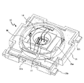
図1は、本実施例における発光装置10において、樹脂部および金属部材が固定された成型体を示す概略的な平面図である。図2は、本実施例における樹脂部および金属部材が一体的に固定された成型体を示す概略的な斜視図である。図3は、本実施例における発光装置10の全体を示す概略的な斜視図である。
図1乃至図3に示すように、本実施例の発光装置10は、発光素子11と、一対の金属部材12a、12bと、発光素子11と金属部材12a、12bとの間を電気的に接続するワイヤ14と、金属部材12a、12bと一体的に固定される樹脂部15と、発光素子11及びワイヤ14を封止する封止樹脂18とを備えて構成されている。また、この発光装置10には、樹脂部15の内部において、金属部材12aまたは金属部材12bに電気的に接続された保護素子13がさらに搭載されている。
FIG. 1 is a schematic plan view showing a molded body in which a resin portion and a metal member are fixed in the
As shown in FIGS. 1 to 3, the light-emitting
金属部材12a、12bは、銅を主成分とする金属材料からなる板状体であり、正負の対を構成している。金属部材12aは、発光素子を搭載する領域と、概形が略直方体の樹脂部15の2つの側面から突出し、所定方向(例えば、X方向)に延びる先端領域(外部端子)とを備えている。また、金属部材12aの発光素子を搭載する領域には、深さ約0.6mm程度の略円柱状の凹部16が形成されている。また、金属部材12aは、発光素子を搭載する領域と、ワイヤが金属部材12aに設けられる(ボンディングされる)領域との間に溝部17が形成されている。本形態における溝部17は、金属部材12aの一部が厚さ方向に貫通されることにより形成されており、溝部17の内側には樹脂部15の一部が延在して設けられている。金属部材12bの一部は、樹脂部15の側面から突出されており、所定方向(例えば、X方向)に延びる外部電極接続用端子とされている。金属部材12aまたは金属部材12bは、それぞれ、樹脂部15からの突出部分の近傍であって、樹脂部15の内部において、途中2箇所で屈曲することにより、凹部を有する上面と、先端領域の上面との間に高低差(例えば、1mm程度以内)を有している。また、金属部材12aまたは金属部材12bは、その先端が突出する樹脂部15の側面とは異なる側面から露出するよう延びる突出部12cを備えており、その突出部12cが延びる方向は、金属部材12a、12bの先端(外部端子)に対して、略垂直となる方向(例えば、Y方向)である。
The
樹脂部15の成形体は、金属部材12の一部を挟持して一体的に、直方体に近い形状(6.5×6.5×1.5mm)で成形されている。成形体は、その中央付近に、略八角形(直径5mm)の発光窓15aを有している。発光窓15a内では、金属部材12a、12bの一部が露出しており、露出した金属部材12の上であって、凹部の中に発光素子11が搭載されている。なお、発光窓15a内には、図3に示したように、レンズ形状に成形された透光性の封止樹脂18が配置されている。
The molded part of the
発光素子11は、その表面に正負一対の電極(図示せず)が2つずつ形成されており、各電極が、金属部材12a、12bと、ワイヤ14によってそれぞれ電気的に接続されている。なお、発光素子11は、発光装置10の略中央、つまり、正負一対の金属部材12a、12bに対する中心線上に配置されている。
The
ワイヤは、ワイヤボンディングにより、金属部材表面及び電極表面に接続されており、金属部材12aとのワイヤ接続の箇所は、凹部の外側である。ワイヤの接続方向は、金属部材12a、12bの先端領域(外部端子)が延びる方向(例えば、図中X方向)と略垂直に交差している(例えば、図中Y方向)。
The wire is connected to the surface of the metal member and the surface of the electrode by wire bonding, and the place of wire connection with the
このように、この発光装置10では、ワイヤの接続方向が、外部端子が延びる方向と略垂直に交差しているため、ワイヤが断線し易い方向に応力がかかることを最大限に防止することができ、ワイヤの断線を抑制することができる。
また、1つの金属部材12a又は12bが、対向する樹脂部15の側面から、反対方向に延びているため、金属部材にかかる引張応力を、互いに相殺することができるため、金属部材が安定し、ワイヤへ応力が伝わることを緩和することができる。
As described above, in the
In addition, since one
さらに、発光素子を、金属部材12a、12bに対する中心線上に配置することにより、応力が集中する中央部分において、ワイヤが通っていない状態を確保することができ、ワイヤの断線防止の効果をさらに向上させることができる。
また、金属部材12aのワイヤが接続される領域と発光素子が配置された領域との間に、溝部17を設けることにより、金属部材12aからワイヤ14の接続部への接合部材(図示せず)の漏れを軽減することができる。あるいは、金属部材12aのワイヤが接続される領域と発光素子が配置された領域との間に、溝部17を設け、この溝部17の上にワイヤを通過させて張る。これにより、金属部材の変形による応力が溝部で緩和されるため、ワイヤにかかる応力は低減される。これにより、金属部材12aにワイヤ14を接続した際の接続部の接合強度を維持できる。
Furthermore, by arranging the light emitting element on the center line with respect to the
Further, by providing the
さらに、図2に示されるように、金属部材12aおよび金属部材12bの一部に設けられた突出部12cが樹脂部15の側面に露出している。そのため、突出部12cが空気と接する面を確保することができる放熱性を向上させることができるとともに、通電時に、発光素子11部分の温度を低減させ、発光装置10全体の温度を低下させることが可能となる。加えて、発光素子11上のワイヤ14接続部の疲労を軽減することができる。
Further, as shown in FIG. 2, the protruding portion 12 c provided on a part of the
なお、本発明の効果を確認するために、図4(a)に示したように、上記実施例1に準じた構成であるが、熱に起因する応力分布を簡便にシミュレートし得る発光装置を設定するとともに、比較のために、図4(b)に示した従来の構成の発光装置を設定した。
つまり、図4(a)の発光装置は、ワイヤ24の接続方向が、樹脂部から突出する金属部材22a、22bの先端が延びる方向と略垂直に交差したものであり、一方、図4(b)の発光装置は、ワイヤ24の接続方向が、樹脂部から突出する金属部材23a、23bの先端が延びる方向と略平行にしたものである。
これらの発光装置を用いて、市販の応力解析ソフト(「ANSYS Professional」、サイバネットシステム社)による線径構造解析を行った。
In order to confirm the effect of the present invention, as shown in FIG. 4A, the light emitting device has a configuration similar to that of Example 1 but can easily simulate the stress distribution caused by heat. And a conventional light emitting device shown in FIG. 4B was set for comparison.
That is, in the light emitting device of FIG. 4A, the connection direction of the
Using these light emitting devices, wire diameter structure analysis was performed using a commercially available stress analysis software (“ANSYS Professional”, Cybernet Systems).
なお、シミュレーション条件は、温度荷重:25℃(常温)から260℃(リフロー実装温度)へ加熱、封止樹脂物性 弾性率:2×10⁶[Pa]、ポアソン比:0.49、線膨張係数:3×10⁻⁴、ワイヤ:Au線、基台および金属部材:銅、成形樹脂:PPAとした。 The simulation conditions were as follows: temperature load: heating from 25 ° C. (room temperature) to 260 ° C. (reflow mounting temperature), sealing resin properties Elastic modulus: 2 × 10 6 [Pa], Poisson's ratio: 0.49, linear expansion coefficient : 3 × 10 −4 , wire: Au wire, base and metal member: copper, molding resin: PPA.
両者を比較したところ、図4(a)に示したように、ワイヤの接続方向が、金属部材先端の延長方向と略垂直に交差したものと、図4(b)の平行なものとは、いずれも、発光素子11のワイヤの接続部分に最も応力がかかるが、応力の最大値は、前者において、後者の約75%にまで、応力緩和が認められた。
When both were compared, as shown in FIG. 4 (a), the connection direction of the wire intersected with the extending direction of the tip of the metal member substantially perpendicularly and the parallel one in FIG. 4 (b) In any case, the stress is most applied to the wire connection portion of the
図5は、本実施例における発光装置30の全体を示す概略的な平面図である。図6は、本実施例における樹脂部および金属部材が一体的に固定された成型体を示す概略的な斜視図である。図7は、本実施例における発光装置30の全体を示す概略的な斜視図である。図8は、本実施例における発光装置30の全体を示す概略的な断面図である。
本実施例における発光装置30は、図5乃至図8に示すように、上記実施例1における発光素子11を載置するための領域と、外部端子とが一体となった金属部材12aに代えて、実施例1と同様の凹部が形成された基台36と、金属部材32aとを用い、さらに金属部材12bに代えて、形状が若干異なる金属部材32bを用い、樹脂部35により設けられる発光窓35aの形状を円形とした。また、金属部材32a、32bは、樹脂部35の側面の一部が凹んで設けられた切り欠き部の壁面から突出された第一の突出部を有している。さらに、金属部材32a、32bは、第一の突出部が設けられた側面とは異なる側面において、第一の突出部よりも高い部位から突出された第二の突出部と、この第二の突出部よりも高い上面を有するように屈曲された金属片と、を含む。
基台36の上面の一部には、凹部を形成する側壁の最上面よりも低い上面が形成されるように段差部を有している。この段差部の上面は、金属部材32a、32bにおいてワイヤがボンディングされる領域と略同一平面上にあり、この段差部の上面に保護素子13が載置されている。ここで、ワイヤがボンディングされる領域は、金属部材の一部に設けられた金属片の上面である。この金属片は、金属部材を形成する工程において、板状の金属部材の一部が短冊状の金属片となるような切り目を入れ、金属部材の主要部と一部が接続した状態で、短冊状の金属片を、金属片の上面が段差部の上面と略同じ高さとなるように、金属片の延長部における二箇所で折り曲げることにより形成されたものである。このような金属片にワイヤを接続することにより、ワイヤの長さを短くすることができる。そのため、ワイヤの下にある樹脂量を少なくすることができ、その結果、樹脂の膨張による影響を最小限にとどめることができ、ワイヤの断線をより低減することができる。
本実施例における基台36は、図6、図7及び図8に示されるように、上面に段差部を有する。この段差部は、樹脂部35の中央部に埋め込まれた略直方体の基台主要部の上に、樹脂部35の上面(凹部の底面)から突出するように、基台主要部より小さい直方体形状の上端部を設けることにより形成させたものである。保護素子13は、発光素子11が収納された凹部を形成している側壁の上面よりも低い段差部の上面に配置されている。このとき、図8に示されるように、段差部の上面に配置された保護素子の上面が、上記側壁の上面よりも低いことが好ましい。これにより、発光素子11の方向から出射される光が保護素子11に遮光されなくなる。そのため、発光装置の出力低下を抑制することができる。
なお、本実施例における保護素子は、同一面側に正負一対の電極を有しており、それぞれの電極がワイヤにより金属部材32aおよび金属部材32bに接続されている。そのため、裏面電極にて電気的に接続する保護素子と異なり、保護素子を配置させた基台に導通をとる必要がなくなる。そおため、基台の材料の選択や発光装置を実装させる基板の設計の自由度が高まり、使い勝手のよい発光装置とすることができる。また、放熱部材として利用される基台が通電による悪影響を受けることがなくなり、発光装置の放熱性を向上させることができる。
FIG. 5 is a schematic plan view showing the entire
As shown in FIGS. 5 to 8, the
A part of the upper surface of the
As shown in FIGS. 6, 7, and 8, the base 36 in the present embodiment has a step portion on the upper surface. The stepped portion has a rectangular parallelepiped shape smaller than the base main portion so as to protrude from the upper surface (bottom surface of the concave portion) of the
In addition, the protection element in a present Example has a pair of positive and negative electrodes on the same surface side, and each electrode is connected to the
また、図6に示したように、樹脂部の内部において、金属部材32aまたは金属部材32bは、ワイヤボンディングされる領域とその他の領域とで高低差を有している。これにより、上述したように、ワイヤの長さを短くすることができ、ひいてはワイヤの断線を防止することができると共に、実装時又は実装後の熱に起因する金属部材等の変形による応力を高さ方向に逃がすことが容易となる。
さらに、図6に示されるように、金属部材32aまたは金属部材32bの一部が第二の突出部32cとして樹脂部35の側面から露出している。これにより、通電時に発生する発光素子41からの熱を効率よく発光装置の外部へ伝えることができ、封止樹脂の膨張率が軽減することによりワイヤ疲労を抑制することができる。
In addition, as shown in FIG. 6, the
Further, as shown in FIG. 6, a part of the
図7は、本実施例における発光装置30の全体を示す概略的な斜視図である。図8は、本実施例における発光装置30の全体を、図5に示された発光素子11および保護素子13の中心を通る水平方向の中心線で切断したときの断面を示す概略図である。
図7および図8に示されるように、本実施例における基台36は、発光素子11が収納された凹部と、その凹部を形成している側壁の上面に配置された保護素子13と、樹脂部35の上面に突出させて形成された環状の壁部47とを被覆する封止樹脂38と、を備える。環状の壁部47は、円形の発光窓35aを形成している側壁であり、封止樹脂38が壁部47の上面および内外壁面に密着して被覆することにより、封止樹脂38が樹脂部35から剥離することがなくなる。さらに、環状の壁部47の外側に、上面から見て略矩形の樹脂部35の外縁に沿って、別の壁部が設けてあり、この壁部と環状の壁部47との間に堀が設けられる。この堀は、封止樹脂38の外縁を包囲するように設けており、封止樹脂38を成型するとき、樹脂部35の上面からの成型材料の漏れ出しが防止される。
また、図6乃至図8に示されるように、本実施例における基台36は、環状の壁部47により樹脂部35に形成された凹部の底面から突出された上端部を有している。この上端部の概形は略直方体であり、発光素子11を収容するために直方体の上面に設けられた開口部は略円形である。また、発光素子11および保護素子13に接続するワイヤは、基台36の上端部の上を通過して張られている。さらに、上端部の概形を略直方体とすることによって設けられた基台上端部の角部および略円形の開口部を封止樹脂38が被覆している。このような形状を有する基台の上端部に封止樹脂38が配置されることにより、上端部およびワイヤ14を被覆する封止樹脂38がワイヤ14に及ぼす応力を低減させることが見出されており、そのため、ワイヤの接続強度が確保された信頼性の高い発光装置とすることができる。
以上説明した他は、実質的に実施例1と同様の構造を有している。なお、同じ構成についてはその説明を省略している(以下の実施例でも同様)。これにより、実施例1と同様の効果を得ることができる。
さらに、金属部材から独立した部材である基台36に発光素子11を配置することにより、通電を行った際の温度上昇による樹脂部の熱膨張を低減することができ、ワイヤにかかる負担をより低減することができる。
FIG. 7 is a schematic perspective view showing the entire
As shown in FIG. 7 and FIG. 8, the base 36 in this embodiment includes a recess in which the
Further, as shown in FIGS. 6 to 8, the base 36 in this embodiment has an upper end portion that protrudes from the bottom surface of the concave portion formed in the
Other than the above description, the structure is substantially the same as that of the first embodiment. The description of the same configuration is omitted (the same applies to the following examples). Thereby, the same effect as Example 1 can be acquired.
Furthermore, by disposing the
図9は、本実施例における発光装置40を示す概略的な平面図である。図10は、本実施例における発光装置40の樹脂部および金属部材が一体的に固定された成型体を示す概略的な斜視図である。
本実施例の発光装置40は、図9及び図10に示すように、発光素子の表面に正負一対の電極が形成された6つの発光素子41と、樹脂部45の同じ側面から先端部が其々突出された一対の金属部材42a、42b、別の一対の金属部材42aa、42bbと、これら発光素子41が載置され、金属部材42a、42aaと、金属部材42b、42bbとに挟持されるように配置した基台46と、発光素子41と金属部材42a乃至42bbとの間をそれぞれ電気的に接続するワイヤ14と、金属部材42a乃至42bbと基台46と一体的に固定する樹脂部45と、各発光素子41とワイヤ14とを封止する封止樹脂(図示せず)と、を備える。さらに、発光装置40は、樹脂部45の上面に形成させた凹部内にて、金属部材42aa、42bbに配置された保護素子13を備えている。
FIG. 9 is a schematic plan view showing the
As shown in FIGS. 9 and 10, the
正負一対の金属部材42a、42aaは、基台46に配置された6つの発光素子のうち、3つの発光素子41の正負一対の電極とそれぞれワイヤ14により接続されている。さらに、正負一対の金属部材42b、42bbは、基台46に配置された6つの発光素子のうち、3つの発光素子41の正負一対の電極とそれぞれワイヤ14により接続されている。なお、発光素子41は、金属部材42a、42aaと、金属部材42b、42bbの延長方向から略同じ距離に想定された中心線上に配置されておらず、それぞれ中心線よりも金属部材42a、42aa側又は金属部材42b、42bb側に配置されている。
また、正負一対の金属部材42a、42aa、正負一対の金属部材42b、42bbは、互いに基台46に対して同じ側に、それぞれ対向するように配置されている。また、各金属部材42a乃至42bbの先端部が樹脂部45から突出しており、外部電極接続用端子とされている。
The pair of positive and
The pair of positive and
さらに、上述した金属部材42a乃至42bbと、発光素子41とを接続するワイヤ14の全ての接続方向は、樹脂部45から突出した金属部材42a乃至42bbの先端が延びる方向と略垂直に交差している。
また、金属部材42a乃至42bbは、それぞれ、樹脂部45からの突出部分の近傍であって、樹脂部45の内部において、2箇所屈曲することにより、凹部を有する上面と、先端領域(外部端子)の上面との間に高低差を有している。
Furthermore, all the connecting directions of the
Further, the
金属部材42a乃至42bbは、それぞれ、外部端子が突出される樹脂部45の側面と異なる方向(略垂直)に延びる突出部42cを有している。
基台46は、樹脂部45の裏面より露出しており、かつ、側面から基台46の一部が突出している。これにより、通電時に発生する発光素子41からの熱を効率よく発光装置の外部へ伝えることができ、封止樹脂の膨張率が軽減することによりワイヤ疲労を抑制することができる。これにより、実施例1と同様の効果を得ることができる。
さらに、複数の発光素子41に対して、複数の正負一対の金属部材42a乃至42bbが設けられているため、それぞれワイヤの距離を短くすることができ、ワイヤにかかる応力を低減することができるとともに、ワイヤ同士の干渉をなくし、ワイヤボンドが容易となる。
Each of the
The
Furthermore, since a plurality of pairs of positive and
本発明の発光装置は、発光素子を搭載することにより、ファクシミリ、コピー機、ハンドスキャナ等における画像読取装置に利用される照明装置のみならず、照明用光源、LEDディスプレイ、携帯電話機等のバックライト光源、信号機、照明式スイッチ、車載用ストップランプ、各種センサおよび各種インジケータ等の種々の照明装置に利用することができる。 The light-emitting device of the present invention is equipped with a light-emitting element, so that not only an illumination device used for an image reading device in a facsimile, a copying machine, a hand scanner, etc., but also a backlight for an illumination light source, an LED display, a mobile phone It can be used for various illumination devices such as a light source, a traffic light, an illumination switch, a vehicle-mounted stop lamp, various sensors, and various indicators.
10、30、40・・・発光装置
11、41・・・発光素子
12a、12b・・・第一の実施例における金属部材
22a、22b・・・本発明の発光装置における金属部材
23a、23b・・・従来の発光装置における金属部材
32a、32b・・・第二の実施例における金属部材
42a、42b、42aa、42bb・・・第三の実施例における金属部材
12c、32c、42c・・・金属部材における第二の突出部
13・・・保護素子
14・・・ワイヤ
15、35、45・・・樹脂部
15a、35a、45a・・・発光窓
16・・・凹部
18、38・・・封止樹脂
36、46・・・基台
47・・・壁部
10, 30, 40...
Claims (6)
前記金属部材は、前記樹脂部内で屈曲されて高低差を有しており、その一部が前記樹脂部から突出された方向と前記ワイヤの接続方向とは、略垂直であり、
前記金属部材は、前記樹脂部からの突出方向が前記ワイヤの接続方向と略垂直とされた第一の突出部と、金属部材の一部が延長され、発光装置の底面からの高さが前記第一の突出部よりも高くなるように屈曲され、前記発光素子の側に配置された金属片と、を有しており、前記発光素子の電極と接続するワイヤが、前記樹脂部から露出された前記金属片の上面に接続されており、
前記金属片の延長方向は、前記第一の突出部の突出方向と略同じであることを特徴とする発光装置。 A light-emitting device comprising: a light-emitting element; a base on which the light-emitting element is placed; a metal member connected to the electrode of the light-emitting element by a wire; and at least a resin part that fixes the base or the metal member. There,
Wherein the metal member has a height difference is bent within the resin portion, the A part and the direction protruding from the resin portion connecting direction of the wire, Ri substantially perpendicular der,
The metal member includes a first protrusion in which a protrusion direction from the resin portion is substantially perpendicular to a connection direction of the wire, a part of the metal member is extended, and a height from a bottom surface of the light emitting device is A metal piece that is bent so as to be higher than the first protrusion and is disposed on the light emitting element side, and a wire that is connected to the electrode of the light emitting element is exposed from the resin part. Connected to the upper surface of the metal piece,
Extending direction of the metal pieces, the light emitting device according to substantially said same der Rukoto the protruding direction of the first projecting portion.
発光装置の底面からの前記第二の突出部の高さは、前記第一の突出部の高さよりも高い請求項1に記載の発光装置。 The metal member has a second protruding portion that protrudes from a side surface different from the side surface on which the first protruding portion is provided,
Height of the second projecting portion from the bottom surface of the light emitting device, light emitting device according to a high claim 1 than the height of the first projecting portion.
Priority Applications (1)
| Application Number | Priority Date | Filing Date | Title |
|---|---|---|---|
| JP2007106386A JP5023781B2 (en) | 2006-11-13 | 2007-04-13 | Light emitting device |
Applications Claiming Priority (3)
| Application Number | Priority Date | Filing Date | Title |
|---|---|---|---|
| JP2006306996 | 2006-11-13 | ||
| JP2006306996 | 2006-11-13 | ||
| JP2007106386A JP5023781B2 (en) | 2006-11-13 | 2007-04-13 | Light emitting device |
Publications (3)
| Publication Number | Publication Date |
|---|---|
| JP2008147611A JP2008147611A (en) | 2008-06-26 |
| JP2008147611A5 JP2008147611A5 (en) | 2010-05-20 |
| JP5023781B2 true JP5023781B2 (en) | 2012-09-12 |
Family
ID=39607406
Family Applications (1)
| Application Number | Title | Priority Date | Filing Date |
|---|---|---|---|
| JP2007106386A Active JP5023781B2 (en) | 2006-11-13 | 2007-04-13 | Light emitting device |
Country Status (1)
| Country | Link |
|---|---|
| JP (1) | JP5023781B2 (en) |
Families Citing this family (18)
| Publication number | Priority date | Publication date | Assignee | Title |
|---|---|---|---|---|
| JP5217800B2 (en) | 2008-09-03 | 2013-06-19 | 日亜化学工業株式会社 | Light emitting device, resin package, resin molded body, and manufacturing method thereof |
| US8598602B2 (en) | 2009-01-12 | 2013-12-03 | Cree, Inc. | Light emitting device packages with improved heat transfer |
| US7923739B2 (en) | 2009-06-05 | 2011-04-12 | Cree, Inc. | Solid state lighting device |
| US9111778B2 (en) | 2009-06-05 | 2015-08-18 | Cree, Inc. | Light emitting diode (LED) devices, systems, and methods |
| US8710525B2 (en) * | 2010-03-15 | 2014-04-29 | Nichia Corporation | Light emitting device |
| US8269244B2 (en) | 2010-06-28 | 2012-09-18 | Cree, Inc. | LED package with efficient, isolated thermal path |
| TW201251140A (en) | 2011-01-31 | 2012-12-16 | Cree Inc | High brightness light emitting diode (LED) packages, systems and methods with improved resin filling and high adhesion |
| JP5941249B2 (en) | 2011-02-02 | 2016-06-29 | 日亜化学工業株式会社 | Light emitting device |
| WO2012109225A1 (en) | 2011-02-07 | 2012-08-16 | Cree, Inc. | Components and methods for light emitting diode (led) lighting |
| JP2013004905A (en) * | 2011-06-21 | 2013-01-07 | Mitsubishi Chemicals Corp | Semiconductor light-emitting device package and semiconductor light-emitting device |
| KR101957884B1 (en) * | 2012-05-14 | 2019-03-13 | 엘지이노텍 주식회사 | Light emitting device, manufactured method of the light emitting deviceand lighting apparatus |
| JP5732619B2 (en) * | 2012-06-27 | 2015-06-10 | パナソニックIpマネジメント株式会社 | LIGHT EMITTING DEVICE AND LIGHTING DEVICE USING THE SAME |
| CN103904207A (en) * | 2014-04-04 | 2014-07-02 | 利亚德光电股份有限公司 | Wafer circuit |
| DE102017100165A1 (en) | 2017-01-05 | 2018-07-05 | Jabil Optics Germany GmbH | Light-emitting device and light-emitting system |
| KR102261288B1 (en) * | 2017-03-14 | 2021-06-04 | 현대자동차 주식회사 | Light emitting diode package for automobile exterior |
| JP6669217B2 (en) * | 2018-08-30 | 2020-03-18 | 日亜化学工業株式会社 | Package and light emitting device using the same |
| JP7054008B2 (en) * | 2019-08-27 | 2022-04-13 | 日亜化学工業株式会社 | Manufacturing method of light emitting device |
| JP2023046654A (en) * | 2021-09-24 | 2023-04-05 | スタンレー電気株式会社 | Light-emitting device and manufacturing method of light-emitting device |
Family Cites Families (3)
| Publication number | Priority date | Publication date | Assignee | Title |
|---|---|---|---|---|
| JP3332809B2 (en) * | 1997-07-10 | 2002-10-07 | 三洋電機株式会社 | Optical element |
| JP3472450B2 (en) * | 1997-09-04 | 2003-12-02 | シャープ株式会社 | Light emitting device |
| JP3908383B2 (en) * | 1998-05-29 | 2007-04-25 | ローム株式会社 | Semiconductor device |
-
2007
- 2007-04-13 JP JP2007106386A patent/JP5023781B2/en active Active
Also Published As
| Publication number | Publication date |
|---|---|
| JP2008147611A (en) | 2008-06-26 |
Similar Documents
| Publication | Publication Date | Title |
|---|---|---|
| JP5023781B2 (en) | Light emitting device | |
| JP5038623B2 (en) | Optical semiconductor device and manufacturing method thereof | |
| JP5528900B2 (en) | Light emitting element module | |
| JP5691681B2 (en) | Light emitting device | |
| US20080128718A1 (en) | Light emitting device | |
| JP5167977B2 (en) | Semiconductor device | |
| JP2009065002A (en) | Light-emitting apparatus | |
| JP2012114311A (en) | Led module | |
| JP5535750B2 (en) | Light emitting element module | |
| JP6064606B2 (en) | Light emitting device | |
| JP5458910B2 (en) | Light emitting device | |
| JP2007280983A (en) | Light-emitting device | |
| US20070228396A1 (en) | Light emitting unit and lighting apparatus | |
| JP6107229B2 (en) | Light emitting device | |
| JP5071069B2 (en) | Light emitting device | |
| JP5206204B2 (en) | Light emitting device | |
| JP5055837B2 (en) | Light emitting device | |
| JP5701843B2 (en) | Light emitting device | |
| JP6191214B2 (en) | Light emitting device | |
| JP4765507B2 (en) | Light emitting device | |
| JP6171295B2 (en) | Light emitting device | |
| KR20110119200A (en) | Light emitting device | |
| JP2014003112A (en) | Lead frame for package, package for light-emitting device and light-emitting device using the same | |
| JP2006024645A (en) | Semiconductor light emitting device | |
| JP5817390B2 (en) | Light emitting device |
Legal Events
| Date | Code | Title | Description |
|---|---|---|---|
| A521 | Request for written amendment filed |
Free format text: JAPANESE INTERMEDIATE CODE: A523 Effective date: 20100407 |
|
| A621 | Written request for application examination |
Free format text: JAPANESE INTERMEDIATE CODE: A621 Effective date: 20100412 |
|
| A521 | Request for written amendment filed |
Free format text: JAPANESE INTERMEDIATE CODE: A523 Effective date: 20110517 |
|
| A131 | Notification of reasons for refusal |
Free format text: JAPANESE INTERMEDIATE CODE: A131 Effective date: 20120117 |
|
| A977 | Report on retrieval |
Free format text: JAPANESE INTERMEDIATE CODE: A971007 Effective date: 20120118 |
|
| A521 | Request for written amendment filed |
Free format text: JAPANESE INTERMEDIATE CODE: A523 Effective date: 20120319 |
|
| TRDD | Decision of grant or rejection written | ||
| A01 | Written decision to grant a patent or to grant a registration (utility model) |
Free format text: JAPANESE INTERMEDIATE CODE: A01 Effective date: 20120522 |
|
| A01 | Written decision to grant a patent or to grant a registration (utility model) |
Free format text: JAPANESE INTERMEDIATE CODE: A01 |
|
| A61 | First payment of annual fees (during grant procedure) |
Free format text: JAPANESE INTERMEDIATE CODE: A61 Effective date: 20120604 |
|
| FPAY | Renewal fee payment (event date is renewal date of database) |
Free format text: PAYMENT UNTIL: 20150629 Year of fee payment: 3 |
|
| R150 | Certificate of patent or registration of utility model |
Ref document number: 5023781 Country of ref document: JP Free format text: JAPANESE INTERMEDIATE CODE: R150 Free format text: JAPANESE INTERMEDIATE CODE: R150 |
|
| FPAY | Renewal fee payment (event date is renewal date of database) |
Free format text: PAYMENT UNTIL: 20150629 Year of fee payment: 3 |
|
| R250 | Receipt of annual fees |
Free format text: JAPANESE INTERMEDIATE CODE: R250 |
|
| R250 | Receipt of annual fees |
Free format text: JAPANESE INTERMEDIATE CODE: R250 |
|
| R250 | Receipt of annual fees |
Free format text: JAPANESE INTERMEDIATE CODE: R250 |
|
| R250 | Receipt of annual fees |
Free format text: JAPANESE INTERMEDIATE CODE: R250 |
|
| R250 | Receipt of annual fees |
Free format text: JAPANESE INTERMEDIATE CODE: R250 |
|
| R250 | Receipt of annual fees |
Free format text: JAPANESE INTERMEDIATE CODE: R250 |
|
| R250 | Receipt of annual fees |
Free format text: JAPANESE INTERMEDIATE CODE: R250 |
|
| R250 | Receipt of annual fees |
Free format text: JAPANESE INTERMEDIATE CODE: R250 |