JP5071069B2 - Light emitting device - Google Patents
Light emitting device Download PDFInfo
- Publication number
- JP5071069B2 JP5071069B2 JP2007305489A JP2007305489A JP5071069B2 JP 5071069 B2 JP5071069 B2 JP 5071069B2 JP 2007305489 A JP2007305489 A JP 2007305489A JP 2007305489 A JP2007305489 A JP 2007305489A JP 5071069 B2 JP5071069 B2 JP 5071069B2
- Authority
- JP
- Japan
- Prior art keywords
- light emitting
- metal member
- emitting element
- emitting device
- resin
- Prior art date
- Legal status (The legal status is an assumption and is not a legal conclusion. Google has not performed a legal analysis and makes no representation as to the accuracy of the status listed.)
- Expired - Fee Related
Links
Images

Classifications
-
- H—ELECTRICITY
- H10—SEMICONDUCTOR DEVICES; ELECTRIC SOLID-STATE DEVICES NOT OTHERWISE PROVIDED FOR
- H10W—GENERIC PACKAGES, INTERCONNECTIONS, CONNECTORS OR OTHER CONSTRUCTIONAL DETAILS OF DEVICES COVERED BY CLASS H10
- H10W72/00—Interconnections or connectors in packages
- H10W72/50—Bond wires
- H10W72/541—Dispositions of bond wires
- H10W72/547—Dispositions of multiple bond wires
- H10W72/5473—Dispositions of multiple bond wires multiple bond wires connected to a common bond pad
-
- H—ELECTRICITY
- H10—SEMICONDUCTOR DEVICES; ELECTRIC SOLID-STATE DEVICES NOT OTHERWISE PROVIDED FOR
- H10W—GENERIC PACKAGES, INTERCONNECTIONS, CONNECTORS OR OTHER CONSTRUCTIONAL DETAILS OF DEVICES COVERED BY CLASS H10
- H10W72/00—Interconnections or connectors in packages
- H10W72/50—Bond wires
- H10W72/551—Materials of bond wires
- H10W72/552—Materials of bond wires comprising metals or metalloids, e.g. silver
- H10W72/5522—Materials of bond wires comprising metals or metalloids, e.g. silver comprising gold [Au]
-
- H—ELECTRICITY
- H10—SEMICONDUCTOR DEVICES; ELECTRIC SOLID-STATE DEVICES NOT OTHERWISE PROVIDED FOR
- H10W—GENERIC PACKAGES, INTERCONNECTIONS, CONNECTORS OR OTHER CONSTRUCTIONAL DETAILS OF DEVICES COVERED BY CLASS H10
- H10W72/00—Interconnections or connectors in packages
- H10W72/851—Dispositions of multiple connectors or interconnections
- H10W72/874—On different surfaces
- H10W72/884—Die-attach connectors and bond wires
-
- H—ELECTRICITY
- H10—SEMICONDUCTOR DEVICES; ELECTRIC SOLID-STATE DEVICES NOT OTHERWISE PROVIDED FOR
- H10W—GENERIC PACKAGES, INTERCONNECTIONS, CONNECTORS OR OTHER CONSTRUCTIONAL DETAILS OF DEVICES COVERED BY CLASS H10
- H10W90/00—Package configurations
- H10W90/701—Package configurations characterised by the relative positions of pads or connectors relative to package parts
- H10W90/751—Package configurations characterised by the relative positions of pads or connectors relative to package parts of bond wires
- H10W90/754—Package configurations characterised by the relative positions of pads or connectors relative to package parts of bond wires between a chip and a stacked insulating package substrate, interposer or RDL
Landscapes
- Led Device Packages (AREA)
- Led Devices (AREA)
Description
本発明は、発光装置に関し、より詳細には、発光ダイオード等の発光素子を使用した発光装置に関する。 The present invention relates to a light emitting device, and more particularly to a light emitting device using a light emitting element such as a light emitting diode.
今日、半導体発光素子を用いた情報末端機器は、光プリンタなどとして重要な位置を占めている。特に、RGB(赤色系、緑色系、青色系)がそれぞれ高輝度に発光可能な導体発光素子が開発されたことに伴い、フルカラー化が可能となった。
たとえば、赤色系LED、緑色系LEDおよび青色系LEDをそれぞれ実装したリードフレームを一定間隔をあけて絶縁するように保持してなる発光装置が知られている。
しかし、このような発光装置は、各リードフレームが接触しないよう、離間させなければならないことから、各素子が離れて配置されることになり、このため光の混色性が悪くなるという問題がある。
Today, information terminal devices using semiconductor light emitting devices occupy an important position as optical printers and the like. In particular, with the development of conductor light emitting elements capable of emitting RGB (red, green, and blue) with high brightness, full colorization has become possible.
For example, a light emitting device is known in which lead frames each mounting a red LED, a green LED, and a blue LED are held so as to be insulated at a predetermined interval.
However, since such a light emitting device must be separated so that the lead frames do not come into contact with each other, the respective elements are arranged apart from each other, and there is a problem that the color mixing property of light deteriorates. .
これに対し、赤色系LED、緑色LEDおよび青色LEDに個別に電圧を印加するために、それぞれ独立したリードフレームを互いに絶縁し、それらリードフレームのうちのひとつに、赤色系LEDの底面に形成された電極、緑色LEDおよび青色LED双方の底面に形成された絶縁性基板が接するように載置された発光装置が提案されている(例えば、特許文献1)。この発光装置では、このような構成により、小型化を図りながら各色の光の混色性を向上させている。 On the other hand, in order to individually apply voltages to the red LED, green LED, and blue LED, independent lead frames are insulated from each other, and one of the lead frames is formed on the bottom surface of the red LED. There has been proposed a light emitting device that is placed so that insulating substrates formed on the bottom surfaces of both the green LED and the blue LED are in contact with each other (for example, Patent Document 1). With this configuration, the light emitting device improves the color mixing of the light of each color while reducing the size.
しかし、駆動速度の高速化、発光素子の高輝度化や長時間使用時など、より厳しい環境下において、上記のような半導体発光素子を利用した光源部を駆動させると、発光素子自体の駆動に伴う発熱により、発光素子から放出される発光波長がずれる。特に、波長の変動幅の大きい発光素子と熱源となり得るような発熱量の大きい発光素子とを同一基材上、同一層上に近接して載置すると、昇温に伴って色バランスが崩れる。このような色バランスの崩れは、電気的/光学的特性を用いてセンシングするスキャナー、光プリンタ機器のように極わずかの特性変動によって、致命的な悪影響を招くこととなる。 However, driving the light source unit using the semiconductor light-emitting element as described above in more severe environments such as higher driving speed, higher brightness of the light-emitting element, and long-time use can drive the light-emitting element itself. Due to the generated heat, the emission wavelength emitted from the light emitting element is shifted. In particular, when a light emitting element having a large wavelength fluctuation range and a light emitting element having a large calorific value that can serve as a heat source are placed close to each other on the same substrate and the same layer, the color balance is lost as the temperature rises. Such a loss of color balance causes a fatal adverse effect due to a slight change in characteristics such as a scanner or an optical printer device that senses using electrical / optical characteristics.
そこで、本発明は、色の混色性を向上させるとともに、色バランスの不均一化を最小限に止めることができる高品質な発光装置を提供することを目的とする。 Accordingly, an object of the present invention is to provide a high-quality light-emitting device capable of improving color mixing properties and minimizing uneven color balance.
本発明の発光装置は、上面に第1の半導体発光素子が搭載された第1の金属部材と、
上面に第2の半導体発光素子が搭載され第2の金属部材と、
前記第1の半導体発光素子および前記第2の半導体発光素子からの光を取り出すことが可能な窓部を上面に有する樹脂パッケージと、を有する発光装置であって、
前記第2の金属部材は、その周縁部が中央部よりも膜厚(「板厚」ともいう、以下同じ)が薄く、前記第2の半導体発光素子が搭載された領域の裏面が、前記樹脂パッケージから露出しており、
前記第1の金属部材は、その裏面が前記周縁部の上面と対向していることを特徴とする。
この発光装置においては、前記第1の半導体発光素子と前記第2の半導体発光素子とは、異なる波長を発光することが好ましい。
また、前記第2の金属部材は、その裏面が前記樹脂パッケージの裏面から露出していることが好ましい。
さらに、前記薄膜(「薄板」ともいう、以下同じ)の周縁部は、角部に切欠を有しており、前記樹脂パッケージは、その裏面であって、少なくとも1つの前記角部の切欠に対応する位置に、凹部を有することが好ましい。
また、前記薄膜状の周縁部には、角部以外の一部において、薄膜状(「薄板状」ともいう、以下同じ)の周縁部よりもさらに膜厚が薄い極薄部が形成されており、該極薄膜部の側面に側方に突出する突起を有することが好ましい。
さらに、前記樹脂パッケージから露出した第2の金属部材は、裏面からの平面視において、角部に切欠を有する突出部を有していることが好ましい。
The light-emitting device of the present invention includes a first metal member having a first semiconductor light-emitting element mounted on the upper surface,
A second metal light-emitting element having a second semiconductor light-emitting element mounted on the upper surface;
A resin package having a window portion on the top surface through which light from the first semiconductor light emitting element and the second semiconductor light emitting element can be extracted,
The peripheral edge portion of the second metal member is thinner than the center portion (also referred to as “plate thickness”, hereinafter the same), and the back surface of the region where the second semiconductor light emitting element is mounted is the resin. Exposed from the package,
The back surface of the first metal member is opposed to the top surface of the peripheral edge.
In the light emitting device, it is preferable that the first semiconductor light emitting element and the second semiconductor light emitting element emit light having different wavelengths.
Moreover, it is preferable that the back surface of the second metal member is exposed from the back surface of the resin package.
Further, a peripheral edge portion of the thin film (also referred to as “thin plate”, hereinafter the same) has a cutout at a corner portion, and the resin package corresponds to at least one cutout of the corner portion on the back surface thereof. It is preferable to have a recess in the position to be.
In addition, the thin film-shaped peripheral part is formed with an ultrathin part that is thinner than the thin film-like (also referred to as “thin plate” hereinafter) peripheral part in a part other than the corner part. It is preferable that the side surface of the ultrathin film portion has a protrusion protruding sideways.
Furthermore, it is preferable that the 2nd metal member exposed from the said resin package has a protrusion part which has a notch in a corner | angular part in planar view from a back surface.
本発明によれば、2つの発光素子を異なる部材上に載置することができるとともに、それらの距離を最小限とすることにより、長時間使用時などのより厳しい環境下においても、駆動速度の高速化及び発光素子の高輝度化の要求を満足させながら、色バランスの不均一化を防止し、色の混色性を向上させることができる高品質の発光装置が得られる。 According to the present invention, the two light emitting elements can be mounted on different members, and by minimizing the distance between them, the driving speed can be reduced even under more severe environments such as long-time use. A high-quality light-emitting device that can prevent uneven color balance and improve color mixing can be obtained while satisfying the demand for higher speed and higher brightness of the light-emitting element.
本発明の発光装置は、主として、第1及び第2の半導体発光素子(以下、単に「発光素子」を記す場合がある)と、これら発光素子を載置する第1及び第2の金属部材と、樹脂パッケージとから構成される。 The light-emitting device of the present invention mainly includes first and second semiconductor light-emitting elements (hereinafter sometimes simply referred to as “light-emitting elements”), and first and second metal members on which these light-emitting elements are mounted. And a resin package.
(半導体発光素子)
発光素子は、半導体からなるものであればよいが、いわゆる発光ダイオードと呼ばれる素子が好ましい。例えば、基板上に、InN、AlN、GaN、InGaN、AlGaN、InGaAlN等の窒化物半導体、III-V族化合物半導体、II-VI族化合物半導体等、種々の半導体によって、活性層を含む積層構造が形成され、一対の電極を有するものが挙げられる。電極は、対向する面に正および負の電極がそれぞれ形成されたものであってもよく、同一面側に正および負の電極がともに形成されていてもよい。この場合の正および負の電極は、必ずしも1つずつ形成されていなくてもよく、それぞれ2つ以上形成されていてもよい。
(Semiconductor light emitting device)
The light emitting element may be made of a semiconductor, but an element called a so-called light emitting diode is preferable. For example, a stacked structure including an active layer is formed on a substrate by various semiconductors such as nitride semiconductors such as InN, AlN, GaN, InGaN, AlGaN, and InGaAlN, III-V compound semiconductors, II-VI compound semiconductors, etc. Examples include those formed and having a pair of electrodes. The electrodes may have positive and negative electrodes formed on opposite surfaces, respectively, and both positive and negative electrodes may be formed on the same surface side. In this case, the positive and negative electrodes do not necessarily have to be formed one by one, and two or more each may be formed.
本発明の発光装置では、少なくとも第1及び第2の発光素子が搭載されている。これらの2つの発光素子は、同じ種類のものが2つ搭載されていてもよいが、発熱量の異なるものであることが好ましい。発熱量の差異は特に限定されないが、通常、上述した半導体材料の種類に起因する発熱量の差異とすることができる。また、発熱量の異なる2種類の発光素子は、活性層から照射される光の波長が異なるものと言い換えることができる。両者の発熱量の差異の程度は特に限定されるものではなく、例えば、赤色系の発光素子と、緑色系又は青色系の発光素子との間の差異を例示することができる。また、2つの発光素子のみでなく、3つ以上の発光素子が搭載されているものであってもよい。この場合、2種類の異なる発熱量又は波長の発光素子でもよいし、3種以上の異なる発熱量又は波長の発光素子でもよい。 In the light emitting device of the present invention, at least the first and second light emitting elements are mounted. These two light emitting elements may be mounted two of the same type, but preferably have different calorific values. Although the difference in the heat generation amount is not particularly limited, it can be usually the difference in the heat generation amount due to the above-described types of semiconductor materials. In other words, the two types of light emitting elements having different calorific values can be said to have different wavelengths of light emitted from the active layer. The degree of the difference between the heat generation amounts of the two is not particularly limited. For example, the difference between a red light emitting element and a green light emitting element or a blue light emitting element can be exemplified. Further, not only two light emitting elements but also three or more light emitting elements may be mounted. In this case, two types of light emitting elements having different heat generation amounts or wavelengths may be used, or three or more types of light emitting elements having different heat generation amounts or wavelengths may be used.
この発光素子は、後述する金属部材に搭載される。発光素子を金属部材に搭載するためには、接合部材が用いられる。例えば、青又は緑発光を有し、サファイア基板上に窒化物半導体を成長させた発光素子の場合には、エポキシ樹脂、シリコーン等の樹脂部材を用いることができる。また、発光素子からの光や熱による樹脂部材の劣化を考慮して、発光素子裏面にAlメッキをしてもよい。また、接合部材として樹脂を使用せず、Au−Sn共晶などの半田、低融点金属等のろう材を用いてもよい。さらに、GaAs等からなり、赤色発光を有する発光素子のように、両面に電極が形成された発光素子の場合には、銀、金、パラジウムなどの導電性ペースト等によってダイボンディングしてもよい。
また、この発光素子は、通常、後述する金属部材とワイヤによって電気的に接続されている。ワイヤは、発光素子の電極とのオーミック性が良好であるか、機械的接続性が良好であるか、電気伝導性及び熱伝導性が良好なものであることが好ましい。熱伝導率としては、0.01cal/S・cm2・℃/cm程度以上が好ましく、さらに0.5cal/S・cm2・℃/cm程度以上がより好ましい。作業性などを考慮すると、ワイヤの直径は、10μm〜45μm程度であることが好ましい。このようなワイヤの材料としては、例えば、金、銅、白金、アルミニウム等の金属及びそれらの合金が挙げられる。なかでも、接合信頼性、接合後の応力緩和等の観点から、金が好ましい。
This light emitting element is mounted on a metal member to be described later. In order to mount the light emitting element on the metal member, a bonding member is used. For example, in the case of a light-emitting element that emits blue or green light and has a nitride semiconductor grown on a sapphire substrate, a resin member such as epoxy resin or silicone can be used. In consideration of deterioration of the resin member due to light or heat from the light emitting element, Al plating may be performed on the back surface of the light emitting element. Also, a resin such as Au—Sn eutectic or solder such as a low melting point metal may be used without using a resin as the bonding member. Furthermore, in the case of a light emitting element made of GaAs or the like and having electrodes formed on both sides thereof, such as a light emitting element that emits red light, die bonding may be performed using a conductive paste such as silver, gold, or palladium.
Moreover, this light emitting element is normally electrically connected with the metal member mentioned later and a wire. It is preferable that the wire has a good ohmic property with the electrode of the light emitting element, a good mechanical connectivity, or a good electrical conductivity and thermal conductivity. The thermal conductivity, preferably 0.01cal / S · cm 2 · ℃ / than about cm further 0.5cal / S · cm 2 · ℃ / cm or higher order is more preferable. Considering workability and the like, the diameter of the wire is preferably about 10 μm to 45 μm. Examples of such a wire material include metals such as gold, copper, platinum, and aluminum, and alloys thereof. Among these, gold is preferable from the viewpoints of bonding reliability, stress relaxation after bonding, and the like.
(金属部材)
金属部材は、通常、発光素子と電気的に接続するための電極及び/又は発光素子を搭載する基台としての役割を果たすものであり、特に、第1の金属部材は、主として、電極及び基台としての役割を果たし、第2の金属部材は、主として基台の役割を果たす。なお、本発明においては、第1及び第2の金属部材以外に、1又は2以上のさらなる金属部材が設けられていてもよい。このような金属部材には、上述したように、2種類の異なる発光素子と同じ又は異なる種類の発光素子が、1個以上、搭載されていてもよい。
(Metal member)
The metal member usually serves as a base for mounting the electrode and / or the light emitting element for electrical connection with the light emitting element. In particular, the first metal member mainly includes the electrode and the base. The second metal member mainly serves as a base, serving as a base. In the present invention, in addition to the first and second metal members, one or more additional metal members may be provided. As described above, one or more light emitting elements of the same type or different types from two different types of light emitting elements may be mounted on such a metal member.
金属部材は、実質的に板状であればよく、波形板状、凹凸を有する板状であってもよい。その膜厚は均一であってもよいし、部分的に厚膜(「厚板」ともいう、以下同じ)又は薄膜(「薄板」ともいう、以下同じ)であってもよい。材料は特に限定されず、熱伝導率の比較的大きな材料(例えば、200W/(m・K)程度以上)、比較的大きい機械的強度を有するもの、あるいは打ち抜きプレス加工又はエッチング加工等が容易な材料で形成することが好ましい。このような材料で形成することにより、発光素子で発生する熱を効率的に逃がすことができる。具体的には、銅、アルミニウム、金、銀、タングステン、鉄、ニッケル等の金属又は鉄−ニッケル合金、燐青銅等の合金等が挙げられる。また、金属部材の表面には、搭載される発光素子からの光を効率よく取り出すために反射メッキが施されていることが好ましい。 The metal member may be substantially plate-shaped, and may be corrugated plate-shaped or plate-shaped having irregularities. The film thickness may be uniform, or may be partially a thick film (also referred to as “thick plate”, hereinafter the same) or a thin film (also referred to as “thin plate”, hereinafter the same). The material is not particularly limited, and a material having a relatively large thermal conductivity (for example, about 200 W / (m · K) or more), a material having a relatively large mechanical strength, or a punching press process or an etching process is easy. It is preferable to form with a material. By forming with such a material, heat generated in the light emitting element can be efficiently released. Specific examples include metals such as copper, aluminum, gold, silver, tungsten, iron and nickel, and alloys such as iron-nickel alloys and phosphor bronze. Moreover, it is preferable that the surface of the metal member is subjected to reflection plating in order to efficiently extract light from the light emitting element to be mounted.
特に、第2の金属部材は、その中央部よりも周縁部において薄膜であることが好ましい(以下、薄膜となった周縁部を、「薄膜の周縁部」と記す)。薄膜の周縁部とは、第2の金属部材の一部又は全部であってもよいし、1ヶ所のみであってもよいし、複数ヶ所にあってもよい。なお、この薄膜の周縁部は、断面形状を見た場合、側面に凸部が形成されているとも言い換えることができる。第2の金属部材の薄膜の周縁部は、その全てが同じ膜厚でなくてもよく、その中央部よりも薄ければ、複数の膜厚又は不均一な膜厚に設定されていてもよい。このような膜厚が異なる部位は、段階的に異なっていてもよいし、傾斜的に異なっていてもよい。また、特定の部位のみに、より薄膜の部位を設けてもよい。薄膜状の周縁部は、第2の金属部材の表面側及び/又は裏面側において薄くなっていてもよいし、部分的に表面側が、部分的に裏面側が薄くなっていてもよいが、表裏面側の双方において部分的又は全体的に薄くなっていることが好ましい。第2の金属部材は、例えば、最も厚膜(厚い)部分(中央部)で0.3mm〜2mm程度、最も薄膜(薄い)部分(薄膜の周縁部)で0.05mm〜0.2mm程度であることが適している。この範囲の薄さとすることにより、後述するように、第1の金属部材とオーバーラップする場合に、厚み方向の長さを最小限にとどめることができるとともに、第2金属部材に十分な放熱効果を発揮させることができる。薄膜状の周縁部の幅は、特に限定されるものではないが、例えば、総長さ4.95mm程度以下であることが適している。このような薄膜状の周縁部を有していることにより、平面積を確保することにより、放熱効果を十分に維持したまま、後述するように、他の金属部材、例えば、第1の金属部材とこの薄膜の周縁部とをオーバーラップさせて、第1及び第2の金属部材上に載置されている発光素子同士の距離を所定の距離又は最小限の距離で配置することができ、色バラツキを低減することができる。しかも、他の金属部材とオーバーラップさせても、厚みを最小限に止めることができ、より小型化を実現することができる。 In particular, the second metal member is preferably a thin film at the peripheral portion rather than the central portion (hereinafter, the peripheral portion that has become a thin film is referred to as a “peripheral portion of the thin film”). The peripheral portion of the thin film may be a part or all of the second metal member, may be only one location, or may be a plurality of locations. In addition, it can be paraphrased that the peripheral part of this thin film has the convex part formed in the side surface, when cross-sectional shape is seen. The peripheral portions of the thin film of the second metal member may not all have the same film thickness, and may be set to a plurality of film thicknesses or non-uniform film thicknesses as long as they are thinner than the central part. . Such portions having different film thicknesses may be different in stages or may be different in an inclined manner. Moreover, you may provide a thin film part only in a specific part. The thin film-shaped peripheral edge portion may be thin on the front surface side and / or the back surface side of the second metal member, or the front surface side may be partially thinned on the front side and the back surface side. It is preferable to be partially or totally thin on both sides. The second metal member is, for example, about 0.3 mm to 2 mm at the thickest (thick) portion (central portion) and about 0.05 mm to 0.2 mm at the thinnest (thin) portion (peripheral portion of the thin film). It is suitable to be. By making the thickness within this range, as will be described later, when overlapping with the first metal member, the length in the thickness direction can be minimized, and a sufficient heat dissipation effect for the second metal member. Can be demonstrated. The width of the thin film-shaped peripheral edge is not particularly limited, but for example, it is suitable that the total length is about 4.95 mm or less. By having such a thin film-like peripheral part, as will be described later, while maintaining a sufficient heat dissipation effect by securing a flat area, other metal members, for example, a first metal member And the peripheral portion of the thin film can be overlapped, and the distance between the light emitting elements mounted on the first and second metal members can be arranged at a predetermined distance or a minimum distance. Variations can be reduced. And even if it overlaps with another metal member, thickness can be stopped to the minimum and more miniaturization can be implement | achieved.
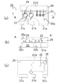
なお、図2(a)〜(c)に示すように、薄膜の周縁部12aが第2の金属部材12の全周囲に存在する場合には、第2の金属部材12自体の形状にかかわらず、第2の金属部材12の薄膜状の周縁部12aの角部が切欠かれた形状(切欠:12d)となっていることが好ましい。いいかえると、平面視における薄膜状の周縁部12aの角部は、その幅が、その辺部と同等かそれよりも小さくなるように形成されているか、その角部に窪みが形成されていることが好ましい。この切欠12dは、平面視における薄膜状の周縁部12aの角部全体が(例えば、幅方向に)切欠かれているよりは、一部のみが切欠かれていることが好ましい。この切欠12dの形状は、段階的に切欠かれた形状、直線的に切欠かれた形状、正方形、ひし形、多角形の一部で角状に欠かれたような形状であってもよいが、円、楕円、放物線の一部で丸く欠かれたような曲面からなる傾斜的な形状であることが好ましい(図2(a)の12d参照)。このような角部の切欠は、第2の金属部材が後述する樹脂パッケージ内に埋め込まれる場合に、第2の金属部材の樹脂パッケージ内でのずれを防止するために利用することができ、適所に第2の金属部材を配置することを可能にする。
As shown in FIGS. 2A to 2C, when the
また、第2の金属部材は、薄膜状の周縁部であって、角部以外の一部において、薄膜状の周縁部よりもさらに薄い極薄部が形成されていることが好ましい。この極薄部は、角部以外の全部に形成されていてもよいし、1ヶ所のみ、2ヶ所以上形成されていてもよい。平面視において、第2の金属部材の対向する辺に、対称に形成されていることが好ましい。また、極薄部は、平面視において、第2の金属部材の薄膜状の周縁部の全幅方向(図2(a)中、矢印Xの方向)に形成されていなくてもよい。これにより、第2金属部材の上面に搭載される第2の発光素子の熱引き効率を妨げることなく発光装置全体の一体性を高めることができる。この極薄部は、例えば、0.3mm程度以下の膜厚(厚さ)、好ましくは0.28mm程度以下の膜厚(厚さ)、幅(図2(a)中、矢印Xの方向)1.0mm程度以下、好ましくは0.8mm程度以下であることが適当である。なお、この極薄部は、薄膜状の周縁部の表面側及び/又は裏面側において薄くなっていてもよいが、部分的に裏面側が薄くなっていることが好ましい。 Moreover, it is preferable that the 2nd metal member is a thin-film-like peripheral part, Comprising: Ultra thin part thinner than a thin-film-like peripheral part is formed in a part other than a corner | angular part. This ultrathin part may be formed in all areas other than the corner part, or may be formed in only one place and two or more places. In plan view, the second metal member is preferably formed symmetrically on the opposite sides. In addition, the ultrathin portion does not have to be formed in the entire width direction (the direction of arrow X in FIG. 2A) of the thin-film peripheral portion of the second metal member in plan view. Thereby, the integrity of the entire light emitting device can be improved without hindering the heat extraction efficiency of the second light emitting element mounted on the upper surface of the second metal member. The ultrathin portion has, for example, a film thickness (thickness) of about 0.3 mm or less, preferably a film thickness (thickness) of about 0.28 mm or less, and a width (in the direction of arrow X in FIG. 2A). It is about 1.0 mm or less, preferably about 0.8 mm or less. In addition, although this ultra-thin part may be thin in the surface side and / or back surface side of a thin film-like peripheral part, it is preferable that the back surface side is partially thinned.
極薄部の側方には、さらに突起が形成されていてもよい。この突起は、第2の金属部材の極薄部における側面に形成されているものであり、通常、この極薄部よりもさらに膜厚が薄い。この突起は、通常、極薄部を形成する場合のバリとして、例えば、上側又は下側からのプレスによるバリとして形成されるが、これにより、樹脂パッケージ内において、樹脂パッケージに食い込むことにより、樹脂パッケージと第2の金属部材の密着性を確実にすることができる。 Further protrusions may be formed on the sides of the ultrathin portion. This protrusion is formed on the side surface of the ultrathin portion of the second metal member, and is usually thinner than this ultrathin portion. This protrusion is usually formed as a burr when forming an ultrathin part, for example, as a burr by pressing from the upper side or the lower side. By this, the resin bites into the resin package in the resin package. The adhesion between the package and the second metal member can be ensured.
第2の金属部材は、その裏面が、後述する樹脂パッケージから露出するように配置されている。ここで、裏面とは、発光素子が載置された面と対向する側の面を指す。これにより、第2の金属部材の放熱効果を向上させることができる。樹脂パッケージの裏面から露出した第2の金属部材の裏面は、第2の金属部材の最も厚膜(厚板)の部分と、薄膜(薄板)状の周縁部とを併せた平面形状から、極薄部の平面形状を差し引いた形状をしており、平面形状において、その角部には、上述した切欠に相当する形状の突出部(図1(c)中、12c参照)を有している。この突出部の形状は、特に限定されるものではなく、一部において切欠を有する三角形、四角形、多角形、円又は扇形及び銀杏葉形状等、ならびにこれに近似する形状及びこれらの一部が変形した形状など、種々の形状とすることができる。このように突出部を有していることにより、樹脂パッケージ裏面のこの部位への半田付け、熱引き部材の接続などを良好にすることができる。 The second metal member is disposed such that the back surface thereof is exposed from a resin package described later. Here, the back surface refers to a surface on the side facing the surface on which the light emitting element is placed. Thereby, the heat dissipation effect of the second metal member can be improved. The back surface of the second metal member exposed from the back surface of the resin package has a planar shape that combines the thickest film (thick plate) portion of the second metal member and the thin film (thin plate) peripheral portion. It has a shape obtained by subtracting the planar shape of the thin portion, and in the planar shape, the corner portion has a protruding portion (see 12c in FIG. 1C) having a shape corresponding to the above-described notch. . The shape of the projecting portion is not particularly limited, and a triangle, a quadrangle, a polygon, a circle or a fan shape and a ginkgo leaf shape, etc. having a notch in a part thereof, and a shape similar thereto and a part thereof are deformed. Various shapes, such as a shaped shape, can be used. Thus, by having a protrusion part, the soldering to this site | part of the resin package back surface, the connection of a heat drawing member, etc. can be made favorable.
なお、第2の金属部材は、上記を満たす形状であれば、その形状については特に限定されないが、通常、薄膜状の周縁部、極薄部、角部の突出部、切欠などを考慮しない基本形状は、多角形、さらに四角形又はそれに近似する形状であることが好ましい。このような形状にすることにより、同面積で効率的な放熱効果を発揮させることができる。 In addition, as long as the second metal member has a shape satisfying the above, the shape is not particularly limited, but usually the basic does not consider a thin film-like peripheral portion, an ultrathin portion, a corner protrusion, a notch, or the like. The shape is preferably a polygon, further a quadrangle, or a shape close thereto. By adopting such a shape, an efficient heat dissipation effect can be exhibited in the same area.
このような第2の金属部材は、その一部が第1の金属部材とオーバーラップするように、後述する樹脂パッケージによって固定されている。つまり、第1の金属部材と樹脂パッケージを介して近傍に設けられる薄膜状の周縁部の上面が、第1の金属部材の裏面と対向している。これにより、厚さ方向の長さを増大させることなく、第2の金属部材上に載置した第2の発光素子と、第1の金属部材上に載置した第1の発光素子との距離をできるだけ短く配置することができる。例えば、第1の金属部材の端部から、表面に第2の発光素子を載置される第2の金属部材の端部までの距離は、0.5mm〜2mm程度が挙げられる。 Such a 2nd metal member is being fixed by the resin package mentioned later so that the part may overlap with a 1st metal member. That is, the upper surface of the thin film-like peripheral portion provided in the vicinity through the first metal member and the resin package is opposed to the back surface of the first metal member. Accordingly, the distance between the second light emitting element placed on the second metal member and the first light emitting element placed on the first metal member without increasing the length in the thickness direction. Can be arranged as short as possible. For example, the distance from the end portion of the first metal member to the end portion of the second metal member on which the second light emitting element is placed on the surface is about 0.5 mm to 2 mm.
通常、金属部材は、発光素子を搭載し、発光素子と接続される領域の他に、外部と接続するリード端子として延長する領域を有している。リード端子は、本発明の発光装置の実装タイプ(例えば、サイドビュータイプ、トップビュータイプなどの表面実装型(SMD)、リード端子を基板などに挿入して用いる挿入型等)、使用態様に応じて、適宜屈曲、変形させることができる。
また、金属部材、例えば、第1の金属部材及び/又は他の金属部材は、発光素子を載置する領域、電気的な接続を行う領域以外に、放熱効率を向上させるために、拡張/幅広部が形成されていてもよい。この場合、拡張/幅広部は、樹脂パッケージ外に及んでいることが好ましい。また、この拡張/幅広部は、樹脂パッケージの外表面に沿って屈曲、変形等されていてもよい。
Usually, the metal member has a region where a light emitting element is mounted and extended as a lead terminal connected to the outside in addition to a region connected to the light emitting element. The lead terminal is a mounting type of the light emitting device of the present invention (for example, a surface mount type (SMD) such as a side view type or a top view type, an insertion type used by inserting a lead terminal into a substrate, etc.) Thus, it can be bent and deformed as appropriate.
Further, the metal member, for example, the first metal member and / or the other metal member is expanded / widened in order to improve the heat dissipation efficiency in addition to the region where the light emitting element is placed and the region where electrical connection is made. A part may be formed. In this case, the extended / wide portion preferably extends outside the resin package. Further, the extended / wide portion may be bent or deformed along the outer surface of the resin package.
(樹脂パッケージ)
本発明の発光装置は、少なくとも、第1及び第2の金属部材が樹脂パッケージにより固定されている。この樹脂パッケージは、複数の金属部材を一体的に又は塊状に、成形、固定、封止又は被覆するものであればよく、一般に、金属部材を固定する成形/固定樹脂と、発光素子及びワイヤ等を被覆する封止/被覆樹脂とによって構成される。いずれの場合においても、材料としての樹脂は、発光素子等に対して、絶縁性を確保することができるものであれば、どのような材料でもよい。例えば、成形/固定樹脂としては、ポリフタルアミド(PPA)、ポリカーボネート樹脂、ポリフェニレンサルファイド(PPS)、液晶ポリマー(LCP)、ABS樹脂、エポキシ樹脂、フェノール樹脂、アクリル樹脂、PBT樹脂等の樹脂等が挙げられる。なかでも、乳白色の樹脂など、遮光性を有する材料であることが好ましい。また、封止/被覆樹脂としては、シリコーン樹脂、ユリア樹脂等の耐候性に優れた透光性の樹脂を用いてもよい。ここで、透光性とは、発光素子から出射された光を70%程度以上、80%程度以上、90%程度以上、95%程度以上透過させる性質を意味する。
成形/固定樹脂と封止/被覆樹脂との組み合わせてにおいては、発光素子等から生じた熱の影響を受けた場合の両者の密着性等を考慮して、互いに熱膨張係数の差が小さいものを選択することが好ましい。
(Resin package)
In the light emitting device of the present invention, at least the first and second metal members are fixed by a resin package. This resin package only needs to be formed, fixed, sealed or covered with a plurality of metal members integrally or in a lump shape. Generally, a molding / fixing resin for fixing a metal member, a light emitting element, a wire, and the like And a sealing / coating resin. In any case, the resin as the material may be any material as long as the insulating property can be secured with respect to the light emitting element or the like. For example, the molding / fixing resin includes polyphthalamide (PPA), polycarbonate resin, polyphenylene sulfide (PPS), liquid crystal polymer (LCP), ABS resin, epoxy resin, phenol resin, acrylic resin, PBT resin, and the like. Can be mentioned. Especially, it is preferable that it is a material which has light-shielding properties, such as milky white resin. Further, as the sealing / coating resin, a translucent resin having excellent weather resistance such as silicone resin and urea resin may be used. Here, the translucency means a property of transmitting light emitted from the light emitting element to about 70% or more, about 80% or more, about 90% or more, or about 95% or more.
In combination of molding / fixing resin and sealing / coating resin, the difference in thermal expansion coefficient between the two is small considering the adhesiveness between the two when affected by the heat generated from the light emitting element, etc. Is preferably selected.
また、これらの材料には、着色剤として、種々の染料又は顔料等を混合して用いてもよい。例えば、Cr2O3、MnO2、Fe2O3、カーボンブラック等が挙げられる。
さらに、これらの材料には、拡散剤又は蛍光物質を含有させてもよい。拡散剤は、光を拡散させるものであり、発光素子からの指向性を緩和させ、視野角を増大させることができる。蛍光物質は、発光素子からの光を変換させるものであり、発光素子から樹脂パッケージの外部へ出射される光の波長を変換することができる。発光素子からの光がエネルギーの高い短波長の可視光の場合、有機蛍光物質であるペリレン系誘導体、ZnCdS:Cu、YAG:Ce、Eu及び/又はCrで賦活された窒素含有CaO−Al2O3−SiO2などの無機蛍光物質など、種々好適に用いられる。
Moreover, you may mix and use various dyes or pigments for these materials as a coloring agent. For example, Cr 2 O 3, MnO 2 , Fe 2 O 3, carbon black and the like.
Further, these materials may contain a diffusing agent or a fluorescent substance. The diffusing agent diffuses light and can reduce the directivity from the light emitting element and increase the viewing angle. The fluorescent substance converts light from the light emitting element, and can convert the wavelength of light emitted from the light emitting element to the outside of the resin package. When the light from the light-emitting element is high-energy short-wavelength visible light, nitrogen-containing CaO—Al 2 O activated with a perylene derivative, ZnCdS: Cu, YAG: Ce, Eu and / or Cr, which is an organic fluorescent material Various inorganic phosphors such as 3- SiO 2 are suitably used.
樹脂パッケージ(成形/固定樹脂)では、その大きさ及び形状は特に限定されるものではなく、例えば、円柱、楕円柱、球、卵形、三角柱、四角柱、多角柱又はこれらに近似する形状等どのような形状でもよいが、発光素子が配置する領域において金属部材が露出するように、あるいは、発光素子からの光を取り出すことができる領域に窓部が形成されていることが好ましい。また、これらの領域において、集光のためのレンズが一体形成されていてもよい。窓部の大きさ及び形状は、本発明の発光装置に搭載される発光素子の合計の占有面積よりも大きければ、特に限定されるものではない。
樹脂パッケージ(成形/固定樹脂)の窓部内の底面及び/又は壁部は、基板及び金属部材と連続した材料であってもよく、電気的接続または放熱経路を形成するため、金属部材の一部が露出していてもよい。樹脂パッケージ(成形/固定樹脂)の窓部の内側には発光素子からの光を反射する反射材料が設けられていてもよく、窓部を封止/被覆する樹脂は、集光のためにリフレクタ形状に形成されていてもよい。
The size and shape of the resin package (molded / fixed resin) are not particularly limited. For example, a cylinder, an elliptical column, a sphere, an oval, a triangular column, a quadrangular column, a polygonal column, or a shape similar to these. Although any shape may be used, it is preferable that a window portion is formed in a region where the metal member is exposed in a region where the light emitting element is disposed or in a region where light from the light emitting element can be extracted. In these regions, a lens for condensing light may be integrally formed. The size and shape of the window portion are not particularly limited as long as it is larger than the total occupied area of the light emitting elements mounted on the light emitting device of the present invention.
The bottom surface and / or the wall portion in the window portion of the resin package (molded / fixed resin) may be a material that is continuous with the substrate and the metal member, and part of the metal member in order to form an electrical connection or a heat dissipation path. May be exposed. A reflective material that reflects light from the light emitting element may be provided inside the window portion of the resin package (molded / fixed resin), and the resin that seals / covers the window portion is a reflector for collecting light. It may be formed in a shape.
この樹脂パッケージ(成形/固定樹脂)は、上述したように、その裏面において、第2の金属部材を露出させており、この第2の金属部材の一部に接触するように、凹部が形成されている。通常、樹脂パッケージ(成形/固定樹脂)は、金属部材(好ましくは、複数)がインサートされて閉じられた金型内に、所定の箇所に形成されたゲートから、溶融した上記材料を流し込み、硬化させることにより、金属部材と一体的に形成される。この場合、成形/固定樹脂による樹脂パッケージを金型から取り出したときに第2の金属部材の一部が裏面において露出するように、第2の金属部材を金型内の所定の位置に配置し、樹脂の流し込みによっても位置ずれを起こさないように固定する必要があり、このような目的のために、金型の一部に(例えば、薄膜の周縁部の角部の切欠に対応する位置に)、位置決めのためのピン部材を挿入し、固定する孔が形成されている。本発明の発光装置の樹脂パッケージ(成形/固定樹脂)においては、このようなピン部材を抜き取った際に、例えば、薄膜の周縁部の角部の切欠に対応する位置に、このようなピン部材の挿入に起因する凹部が形成されている。このような凹部が形成されることにより、例えば、本発明の発光装置を実装基板に実装し、裏面の第2の金属部材の露出部を半田などで固定する際に、余剰の半田等を逃がす空間を確保することができることとなる。 As described above, the resin package (molded / fixed resin) has the second metal member exposed on the back surface thereof, and a recess is formed so as to be in contact with a part of the second metal member. ing. Usually, a resin package (molded / fixed resin) is cured by pouring the molten material from a gate formed at a predetermined position into a mold in which a metal member (preferably a plurality) is inserted and closed. By doing so, it is formed integrally with the metal member. In this case, the second metal member is arranged at a predetermined position in the mold so that a part of the second metal member is exposed on the back surface when the resin package made of molding / fixing resin is taken out of the mold. It is necessary to fix the resin so as not to be displaced even when the resin is poured. For this purpose, a part of the mold (for example, at a position corresponding to a notch at the corner of the peripheral edge of the thin film) ), A hole for inserting and fixing a pin member for positioning is formed. In the resin package (molding / fixing resin) of the light emitting device of the present invention, when such a pin member is extracted, for example, such a pin member is located at a position corresponding to a notch at the corner of the peripheral edge of the thin film. A recess resulting from the insertion of is formed. By forming such a recess, for example, when the light emitting device of the present invention is mounted on a mounting substrate and the exposed portion of the second metal member on the back surface is fixed with solder or the like, excess solder or the like is released. Space can be secured.
本発明の発光装置には、所定の発光素子の他、保護素子が搭載されていてもよい。保護素子は、1つでもよいし、2つ以上の複数個でもよい。ここで、保護素子は、特に限定されるものではなく、発光装置に搭載される公知のもののいずれでもよい。例えば、過熱、過電圧、過電流等に対する保護回路用の素子(例えば、静電保護素子)等が挙げられる。具体的には、ツェナーダイオード、トランジスタダイオード等が利用できる。
さらに、本発明の発光装置は、発光装置の一部として又は樹脂パッケージ(成形/固定樹脂)表面に付属するように、例えば、発光素子の光の出射部(例えば、発光素子の上方)に、プラスチック又は硝子からなるレンズ等が備えられていてもよい。また、発光素子からの光の取り出しを効率的に行うために、反射部材光拡散部材等が備えられていてもよく、光量を調整するための反射防止部材等種々の部材が備えられていてもよい。
The light emitting device of the present invention may be equipped with a protective element in addition to a predetermined light emitting element. The number of protective elements may be one, or two or more. Here, the protective element is not particularly limited, and may be any known element mounted on the light emitting device. For example, an element (for example, an electrostatic protection element) for a protection circuit against overheating, overvoltage, overcurrent, or the like can be given. Specifically, a Zener diode, a transistor diode, or the like can be used.
Further, the light emitting device of the present invention is attached to the surface of the resin package (molded / fixed resin) as a part of the light emitting device, for example, on the light emitting portion of the light emitting element (for example, above the light emitting element), A lens made of plastic or glass or the like may be provided. Further, in order to efficiently extract light from the light emitting element, a reflection member light diffusion member or the like may be provided, or various members such as an antireflection member for adjusting the light amount may be provided. Good.
以下に、本発明の発光装置の実施例を図面に基づいて詳細に説明する。
実施例1
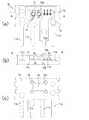
この実施例の発光装置10は、図1(a)〜(c)に示したように、サイドビュータイプの発光装置であって、第1の金属部材11aと、第2の金属部材12と、端子として機能する他の金属部材11b〜11dが、樹脂パッケージ(成形/固定樹脂)15に固定され、これら金属部材11a〜11dの他端が、樹脂パッケージ15の一面において突出して構成されている。
樹脂パッケージ15は、例えば、PBT、PPA等、従来から用いられている樹脂パッケージ材料によって形成されており、その基本形状は、例えば、10mm×14.5mm×1.5mmの大きさの略直方体である。また、その一面に、後述する発光素子から出射される光を取り出すための窓部15aが形成されている。
Embodiments of the light emitting device according to the present invention will be described below in detail with reference to the drawings.
Example 1
The
The
第1の金属部材11a上には、比較的発熱量の小さい3つの発光素子13が載置されている。この発光素子13は、主波長が約630nmの赤色発光を有するAlInGaP/GaAs半導体によって形成されている。この発光素子13は、例えば、銀ペーストによって、第1の金属部材11a上にダイボンディングされている。なお、これら発光素子13の間隔は、0.6mm程度に設定されている。また、この第1の金属部材は、他の金属部材よりも幅が広く設定させている。
On the
第2の金属部材(サイズ:2.1mm×1.2mm)12上には、平面視、略長方形の形状をしており、比較的発熱量の大きな2つの発光素子14が載置されている。このような発光素子14は、例えば、サファイア基板上にn型GaNよりなるn型コンタクト層と、n型AlGaNよりなるn型クラッド層と、InN、AlN、GaN、InGaN、AlGaN、InGaAlN等の窒化物半導体からなる発光層と、p型AlGaN又はInGaNよりなるp型クラッド層と、p型GaNよりなるp型コンタクト層とが順次に積層されて、主波長が約470nmの青色発光を有するInGaN半導体又は主波長が約525nmの緑色発光を有するInGaN半導体によって形成されている。この発光素子14は、例えば、エポキシ樹脂を用いてダイボンディングされている。なお、これら発光素子14の間隔は、1.05mm程度に設定されている。
On the second metal member (size: 2.1 mm × 1.2 mm) 12, two
また、他の金属部材として、発光素子13、14の一方の電極に電気的に接続される金属部材11bと、発光素子14の他方の電極にそれぞれ電気的に接続される金属部材11c、11dとが、樹脂パッケージ15によって、ともに固定されている。金属部材と電極との接続は、例えば、直径10μm程度の金線からなるワイヤによって行われている。
第1の金属部材11a及び他の金属部材11b〜11dは、例えば、0.15mm厚、第2の金属部材12は、例えば、0.85mm厚の銀メッキ銅板を、プレスを用いた打ち抜き加工により形成されたものである。なお、任意に、プレス後にめっきを行ってもよい。また、第2の金属部材12において、後述する薄膜の周縁部12aは、プレス加工し、極薄部12e及び突起12bは、第2の金属部材12の裏面側からのプレスによって、形成することができる。
In addition, as other metal members, a
The
特に、第2の金属部材12は、図2(a)〜(c)に示したように、その全周縁部において、その中央部よりも膜厚が薄い、薄膜状の周縁部12aを有している。この薄膜状の周縁部12aは、上面側の高さが小さくなるように形成されており、例えば、その高さが0.4mm程度、幅(図2(a)中、矢印X)が0.2mm程度である。
また、第2の金属部材12は、平面形状において、薄膜状の周縁部12aの角部が面取りされたような形状の切欠12dを有している。
角部以外の周縁部12aの一部に、この周縁部12aよりもさらに膜厚が薄い極薄部12eが形成されている。この極薄部12eの膜厚(高さ)は、例えば、0.2mm程度であり、下面側の高さが小さくなるように形成されている。この極薄部12eの幅(図2(a)中、矢印X方向の長さ)は、0.2mm程度である。また、極薄部12eは、その側方に突出する突起12bを有している。この突起12bは、極薄部12eが配置する部位の略全側方に形成されている。この突起12bの側方への突出長さ(図2(a)中、矢印X方向の長さ)は0.15mm程度、厚み(高さ)は0.15mm程度である。
In particular, as shown in FIGS. 2A to 2C, the
Moreover, the
An
この第2の金属部材12の裏面は、図1(c)に示すように、樹脂パッケージ15の裏面から露出している。第2の金属部材12の露出形状(裏面からの平面視において)は、上述したように、第2の金属部材12の上面側から高さが小さくなる薄膜状の周縁部12aと、その角部の切欠12dと、第2の金属部材12の下面側から高さが小さくなる極薄部12eとの形状に起因して、基本形状が略長方形であるが、その4つの角部に、面取り様の切欠12dを有する銀杏葉様の突出部12cを有する形状となっている。
The back surface of the
樹脂パッケージ15内では、図1(b)に示すように、第2の金属部材12の薄膜状の周縁部12aの上面に、第1の金属部材11aの一部の裏面が、オーバーラップするように、対向して配置されている。
さらに、樹脂パッケージ15における第2の金属部材12の露出面には、第2の金属部材12の4つの角部の切欠12dに対応する位置に、切欠12dの側面の一部が露出する凹部16を有している。この凹部16は、例えば、直径0.6mm程度の円形で、深さが0.5mm〜0.8mm程度である。
In the
Furthermore, the exposed surface of the
樹脂パッケージ15は、第1、第2、その他の金属部材11a〜11d、12がインサートされて閉じられた金型内に、下面に形成されたゲートから、溶融した樹脂材料を流し込み、硬化させることにより、金属部材と一体的に形成される。この場合、第2の金属部材12を、上述した位置に収めるために、金型の所定の位置にピンを挿入する孔が形成されており、その孔からピンを差し込み、ピンを、第2の金属部材12の突出部12cに形成された切欠12dに当接させ、固定する。樹脂材料を流し込み、樹脂材料を硬化後成形部材をから離型する際、ピンを抜き取る。この際、樹脂パッケージ15の裏面に、ピンの抜き取りに起因する凹部16が形成される。
このような樹脂パッケージ15には、図示しないが、金属部材のいずれかに、保護素子が搭載されている。
また、発光素子13、14が搭載された樹脂パッケージ15の窓部15a内には、エポキシ樹脂からなる透光性被覆材が充填され、硬化されている。
The
Although not shown, such a
In addition, the
このような構成の発光装置によれば、発熱量が異なる2種類の発光素子を、2つの分離された金属部材に載置するために、発熱量の大きな発光素子の熱が、発熱量の小さな発光素子に直接影響を及ぼすことなく、両者の発光波長をずらすことなく、色バランスを長時間にわたって維持することができる。
第2の金属部材の周縁部を薄膜状にすることにより、第1の金属部材の一部をその薄膜状の周縁部にオーバーラップさせることができ、第2の金属部材について放熱を十分に行うことができる平面積を確保しながら、第1の金属部材と第2の金属部材との距離を短くし、ひいては、それらの上に載置された発光素子間の距離を最小限にすることができ、色バランスのずれを防止することができる。
According to the light emitting device having such a configuration, since two types of light emitting elements having different calorific values are placed on two separated metal members, the heat of the light emitting elements having a large calorific value is small. The color balance can be maintained for a long time without directly affecting the light emitting element and without shifting the emission wavelength of both.
By making the peripheral part of the second metal member into a thin film, a part of the first metal member can be overlapped with the peripheral part of the thin film, and the second metal member can sufficiently dissipate heat. The distance between the first metal member and the second metal member can be shortened while ensuring a plane area that can be obtained, and as a result, the distance between the light-emitting elements placed on them can be minimized. The color balance can be prevented from shifting.
また、第2の金属部材の一面が樹脂パッケージの裏面側において露出しているために、より放熱効果を向上させることができる。
さらに、第2の金属部材の薄膜状の周縁部の角部に切欠を有しているため、樹脂パッケージをモールドする際に、切欠の形状を利用して、つまり、この形状に当接するピン等を用いて、第2の金属部材の位置ずれを防止することができ、適所に第2の金属部材を配置することが可能となる。
Moreover, since the one surface of the second metal member is exposed on the back surface side of the resin package, the heat dissipation effect can be further improved.
Further, since the second metal member has a notch at the corner of the thin film-like peripheral edge, when molding the resin package, the shape of the notch is used, that is, a pin that comes into contact with this shape, etc. Can be used to prevent the displacement of the second metal member, and the second metal member can be disposed at an appropriate position.
樹脂パッケージから露出した第2の金属部材の角部に、裏面からの平面視において、角部に対向する部位に切欠を有する突出部が形成されていることにより、より広範囲の面積で半田等と接合することが可能となり、良好な接合/接続を可能にする。
樹脂パッケージの裏面においては、上述した、樹脂のモールド時に利用したピンに起因して、切欠に対応する位置に凹部が形成されることにより、露出した第2の金属部材を半田等により実装基板等に実装する際に、余剰の半田等の逃げ空間を確保することができ、適切な実装/接続を実現することができる。
In the corner portion of the second metal member exposed from the resin package, in a plan view from the back surface, a protrusion having a notch is formed at a portion facing the corner portion, so that solder or the like can be formed over a wider area. It becomes possible to join and allows good joining / connection.
On the back surface of the resin package, a concave portion is formed at a position corresponding to the notch due to the pins used at the time of resin molding described above, so that the exposed second metal member is mounted on the mounting substrate by soldering or the like. When mounting on the board, an escape space for excess solder or the like can be secured, and appropriate mounting / connection can be realized.
第2の金属部材の薄膜状の周縁部の角部以外の一部において、さらに厚みが薄い極薄部が形成されることにより、第2の金属部材の厚み方向の位置ずれ防止の効果を妨げることなく、樹脂パッケージの厚み方向と第2の金属部材との密着性を高めることができる。
また、この極薄部の側方に、突起を有することにより、樹脂パッケージ内において樹脂パッケージに食い込むことにより、樹脂パッケージからの幅方向と第2の金属部材との密着性を確実にすることができる。
By forming an ultrathin portion having a thinner thickness in a portion other than the corners of the thin-film peripheral portion of the second metal member, the effect of preventing the displacement of the second metal member in the thickness direction is hindered. The adhesion between the thickness direction of the resin package and the second metal member can be improved.
In addition, by having a protrusion on the side of this ultrathin portion, it is possible to ensure adhesion between the width direction from the resin package and the second metal member by biting into the resin package in the resin package. it can.
実施例2
この発光装置20は、図3(a)〜(c)に示したように、トップビュータイプの表面実装型発光装置であって、第1の金属部材21aと、第2の金属部材22と、端子として機能する他の金属部材21b〜21dが、樹脂パッケージ25に固定され、これら金属部材21a〜21dの他端が、樹脂パッケージ25の側面から突出し、屈曲して外部端子と機能するように構成されている以外、実質的に、実施例1の発光装置と略同様の構成を有している。
この発光装置20では、樹脂パッケージ25裏面において、第2の金属部材22の切欠に対応して配置された凹部26が対角線状に2つのみ形成されている。
このような構成の発光装置は、実質的に実施例1の発光装置と同様の効果を有する。
Example 2
As shown in FIGS. 3A to 3C, the
In the
The light emitting device having such a configuration has substantially the same effect as the light emitting device of the first embodiment.
照明用光源、各種インジケーター用光源、車載用光源、ディスプレイ用光源、液晶のバックライト用光源などに使用することができる。 It can be used for illumination light sources, various indicator light sources, in-vehicle light sources, display light sources, liquid crystal backlight light sources, and the like.
10、20 発光装置
11a 第1の金属部材
11b、11c、11d 金属部材
12 第2の金属部材
12a 薄膜の周縁部
12b 突起
12c 突出部
12d 切欠
12e 極薄部
13、23 第1の半導体発光素子
14、24 第2の半導体発光素子
15、25 樹脂パッケージ
15a、25a 窓部
16、26 凹部
DESCRIPTION OF
Claims (5)
上面に第2の半導体発光素子が搭載された第2の金属部材と、
前記第1の半導体発光素子および前記第2の半導体発光素子からの光を取り出すことが可能な窓部を上面に有する樹脂パッケージとを有する発光装置であって、
前記第2の金属部材は、その周縁部が第2の半導体発光素子が搭載された領域である中央部よりも膜厚が薄く、前記第2の半導体発光素子が搭載された領域の裏面が、前記樹脂パッケージから露出しており、
前記第1の金属部材は、その裏面が前記周縁部の上面と対向していることを特徴とする発光装置。 A first metal member having a first semiconductor light emitting element mounted on the upper surface;
A second metal member which second semiconductor light emitting element is mounted on the upper surface,
A light emitting device comprising: a resin package having a window portion on a top surface capable of extracting light from the first semiconductor light emitting element and the second semiconductor light emitting element;
The peripheral portion of the second metal member is thinner than the central portion where the second semiconductor light emitting element is mounted, and the back surface of the region where the second semiconductor light emitting element is mounted is Exposed from the resin package,
The light emitting device according to claim 1, wherein a back surface of the first metal member faces an upper surface of the peripheral edge.
Priority Applications (2)
| Application Number | Priority Date | Filing Date | Title |
|---|---|---|---|
| JP2007305489A JP5071069B2 (en) | 2006-12-01 | 2007-11-27 | Light emitting device |
| US11/946,597 US7964892B2 (en) | 2006-12-01 | 2007-11-28 | Light emitting device |
Applications Claiming Priority (3)
| Application Number | Priority Date | Filing Date | Title |
|---|---|---|---|
| JP2006325095 | 2006-12-01 | ||
| JP2006325095 | 2006-12-01 | ||
| JP2007305489A JP5071069B2 (en) | 2006-12-01 | 2007-11-27 | Light emitting device |
Publications (2)
| Publication Number | Publication Date |
|---|---|
| JP2008160091A JP2008160091A (en) | 2008-07-10 |
| JP5071069B2 true JP5071069B2 (en) | 2012-11-14 |
Family
ID=39660619
Family Applications (1)
| Application Number | Title | Priority Date | Filing Date |
|---|---|---|---|
| JP2007305489A Expired - Fee Related JP5071069B2 (en) | 2006-12-01 | 2007-11-27 | Light emitting device |
Country Status (1)
| Country | Link |
|---|---|
| JP (1) | JP5071069B2 (en) |
Families Citing this family (5)
| Publication number | Priority date | Publication date | Assignee | Title |
|---|---|---|---|---|
| DE102006004397A1 (en) | 2005-09-30 | 2007-04-05 | Osram Opto Semiconductors Gmbh | Optoelectronic component, e.g. light emitting diode, has housing with housing material that is permeable for useful radiation and has radiation absorbing particles to adjust predetermined radiation or luminous intensity of radiation |
| DE102007015474A1 (en) | 2007-03-30 | 2008-10-02 | Osram Opto Semiconductors Gmbh | Electromagnetic radiation-emitting optoelectronic component and method for producing an optoelectronic component |
| JP5206204B2 (en) * | 2008-07-31 | 2013-06-12 | 日亜化学工業株式会社 | Light emitting device |
| DE102008045925A1 (en) * | 2008-09-04 | 2010-03-11 | Osram Opto Semiconductors Gmbh | Optoelectronic component and method for producing an optoelectronic component |
| JP6268636B2 (en) | 2014-01-08 | 2018-01-31 | パナソニックIpマネジメント株式会社 | Light emitting device, illumination light source, and illumination device |
Family Cites Families (7)
| Publication number | Priority date | Publication date | Assignee | Title |
|---|---|---|---|---|
| JPH0388472U (en) * | 1989-12-22 | 1991-09-10 | ||
| JP3668438B2 (en) * | 2001-06-07 | 2005-07-06 | シャープ株式会社 | Chip light emitting diode |
| JP2003258465A (en) * | 2002-03-04 | 2003-09-12 | Denso Corp | Electronic circuit unit |
| JP2006093470A (en) * | 2004-09-24 | 2006-04-06 | Toshiba Corp | Lead frame, light emitting device, and method of manufacturing light emitting device |
| JP2006108517A (en) * | 2004-10-08 | 2006-04-20 | Citizen Watch Co Ltd | LED connection substrate, illumination device using the same, and display device using the same |
| JP2006237464A (en) * | 2005-02-28 | 2006-09-07 | Matsushita Electric Ind Co Ltd | Semiconductor light emitting device |
| JP4542453B2 (en) * | 2005-03-24 | 2010-09-15 | 日亜化学工業株式会社 | Light emitting device |
-
2007
- 2007-11-27 JP JP2007305489A patent/JP5071069B2/en not_active Expired - Fee Related
Also Published As
| Publication number | Publication date |
|---|---|
| JP2008160091A (en) | 2008-07-10 |
Similar Documents
| Publication | Publication Date | Title |
|---|---|---|
| US7964892B2 (en) | Light emitting device | |
| JP5119621B2 (en) | Light emitting device | |
| KR101602977B1 (en) | Light-emitting device | |
| JP5691681B2 (en) | Light emitting device | |
| JP5023781B2 (en) | Light emitting device | |
| US7527400B2 (en) | Light emitting device | |
| JP5326229B2 (en) | Light emitting device | |
| US9281460B2 (en) | Light emitting device package and light emitting device having lead-frames | |
| JP5365252B2 (en) | Optical semiconductor device and manufacturing method thereof | |
| JP2009065002A (en) | Light emitting device | |
| JP2004071675A (en) | Light emitting diode | |
| JP5458910B2 (en) | Light emitting device | |
| JP6064396B2 (en) | Light emitting device | |
| JP5071069B2 (en) | Light emitting device | |
| EP1843403B1 (en) | Light emitting unit and lighting apparatus | |
| JP6107229B2 (en) | Light emitting device | |
| JP4961978B2 (en) | Light emitting device and manufacturing method thereof | |
| JP5701843B2 (en) | Light emitting device | |
| JP2008047712A (en) | Light emitting device | |
| JP2007280983A (en) | Light emitting device | |
| JP5722759B2 (en) | Light emitting device | |
| CN103227264B (en) | Light-emitting device |
Legal Events
| Date | Code | Title | Description |
|---|---|---|---|
| A621 | Written request for application examination |
Free format text: JAPANESE INTERMEDIATE CODE: A621 Effective date: 20101102 |
|
| A131 | Notification of reasons for refusal |
Free format text: JAPANESE INTERMEDIATE CODE: A131 Effective date: 20120424 |
|
| A977 | Report on retrieval |
Free format text: JAPANESE INTERMEDIATE CODE: A971007 Effective date: 20120425 |
|
| A601 | Written request for extension of time |
Free format text: JAPANESE INTERMEDIATE CODE: A601 Effective date: 20120622 |
|
| A521 | Request for written amendment filed |
Free format text: JAPANESE INTERMEDIATE CODE: A523 Effective date: 20120626 |
|
| A602 | Written permission of extension of time |
Free format text: JAPANESE INTERMEDIATE CODE: A602 Effective date: 20120627 |
|
| TRDD | Decision of grant or rejection written | ||
| A01 | Written decision to grant a patent or to grant a registration (utility model) |
Free format text: JAPANESE INTERMEDIATE CODE: A01 Effective date: 20120724 |
|
| A01 | Written decision to grant a patent or to grant a registration (utility model) |
Free format text: JAPANESE INTERMEDIATE CODE: A01 |
|
| A61 | First payment of annual fees (during grant procedure) |
Free format text: JAPANESE INTERMEDIATE CODE: A61 Effective date: 20120806 |
|
| R150 | Certificate of patent or registration of utility model |
Ref document number: 5071069 Country of ref document: JP Free format text: JAPANESE INTERMEDIATE CODE: R150 Free format text: JAPANESE INTERMEDIATE CODE: R150 |
|
| FPAY | Renewal fee payment (event date is renewal date of database) |
Free format text: PAYMENT UNTIL: 20150831 Year of fee payment: 3 |
|
| FPAY | Renewal fee payment (event date is renewal date of database) |
Free format text: PAYMENT UNTIL: 20150831 Year of fee payment: 3 |
|
| R250 | Receipt of annual fees |
Free format text: JAPANESE INTERMEDIATE CODE: R250 |
|
| R250 | Receipt of annual fees |
Free format text: JAPANESE INTERMEDIATE CODE: R250 |
|
| R250 | Receipt of annual fees |
Free format text: JAPANESE INTERMEDIATE CODE: R250 |
|
| R250 | Receipt of annual fees |
Free format text: JAPANESE INTERMEDIATE CODE: R250 |
|
| R250 | Receipt of annual fees |
Free format text: JAPANESE INTERMEDIATE CODE: R250 |
|
| R250 | Receipt of annual fees |
Free format text: JAPANESE INTERMEDIATE CODE: R250 |
|
| LAPS | Cancellation because of no payment of annual fees |