JP5010031B2 - Non-volatile memory and method for intra-page and inter-page on-chip data pseudo-randomization - Google Patents
Non-volatile memory and method for intra-page and inter-page on-chip data pseudo-randomization Download PDFInfo
- Publication number
- JP5010031B2 JP5010031B2 JP2010524087A JP2010524087A JP5010031B2 JP 5010031 B2 JP5010031 B2 JP 5010031B2 JP 2010524087 A JP2010524087 A JP 2010524087A JP 2010524087 A JP2010524087 A JP 2010524087A JP 5010031 B2 JP5010031 B2 JP 5010031B2
- Authority
- JP
- Japan
- Prior art keywords
- page
- data
- memory
- programming
- read
- Prior art date
- Legal status (The legal status is an assumption and is not a legal conclusion. Google has not performed a legal analysis and makes no representation as to the accuracy of the status listed.)
- Expired - Fee Related
Links
- 230000015654 memory Effects 0.000 title claims abstract description 238
- 238000000034 method Methods 0.000 title claims description 92
- 230000006870 function Effects 0.000 claims description 22
- 230000001960 triggered effect Effects 0.000 claims description 6
- 230000004044 response Effects 0.000 claims 1
- 238000003860 storage Methods 0.000 abstract description 45
- 238000007667 floating Methods 0.000 abstract description 43
- 230000008878 coupling Effects 0.000 abstract description 15
- 238000010168 coupling process Methods 0.000 abstract description 15
- 238000005859 coupling reaction Methods 0.000 abstract description 15
- 230000007774 longterm Effects 0.000 abstract description 2
- 230000008569 process Effects 0.000 description 33
- 238000006243 chemical reaction Methods 0.000 description 14
- 238000012546 transfer Methods 0.000 description 11
- 238000012795 verification Methods 0.000 description 11
- 238000001514 detection method Methods 0.000 description 10
- 230000000694 effects Effects 0.000 description 8
- 230000005684 electric field Effects 0.000 description 8
- 238000012545 processing Methods 0.000 description 7
- 230000008859 change Effects 0.000 description 6
- 239000000758 substrate Substances 0.000 description 6
- 238000004891 communication Methods 0.000 description 5
- 238000013461 design Methods 0.000 description 5
- 101001072191 Homo sapiens Protein disulfide-isomerase A2 Proteins 0.000 description 4
- 101001098828 Homo sapiens Protein disulfide-isomerase A5 Proteins 0.000 description 4
- 102100036351 Protein disulfide-isomerase A2 Human genes 0.000 description 4
- 238000010586 diagram Methods 0.000 description 4
- 230000000630 rising effect Effects 0.000 description 4
- 230000009471 action Effects 0.000 description 3
- 238000013459 approach Methods 0.000 description 3
- 230000008901 benefit Effects 0.000 description 3
- 230000000295 complement effect Effects 0.000 description 3
- 238000013500 data storage Methods 0.000 description 3
- 238000009792 diffusion process Methods 0.000 description 3
- 238000002347 injection Methods 0.000 description 3
- 239000007924 injection Substances 0.000 description 3
- 230000007246 mechanism Effects 0.000 description 3
- 230000004048 modification Effects 0.000 description 3
- 238000012986 modification Methods 0.000 description 3
- 238000001745 non-dispersive infrared spectroscopy Methods 0.000 description 3
- 230000002093 peripheral effect Effects 0.000 description 3
- VYPSYNLAJGMNEJ-UHFFFAOYSA-N Silicium dioxide Chemical compound O=[Si]=O VYPSYNLAJGMNEJ-UHFFFAOYSA-N 0.000 description 2
- 238000003491 array Methods 0.000 description 2
- 230000006399 behavior Effects 0.000 description 2
- 230000007423 decrease Effects 0.000 description 2
- 238000009826 distribution Methods 0.000 description 2
- 230000005669 field effect Effects 0.000 description 2
- 239000002784 hot electron Substances 0.000 description 2
- 238000004519 manufacturing process Methods 0.000 description 2
- 230000036961 partial effect Effects 0.000 description 2
- 229910021420 polycrystalline silicon Inorganic materials 0.000 description 2
- 229920005591 polysilicon Polymers 0.000 description 2
- 230000001603 reducing effect Effects 0.000 description 2
- 230000002829 reductive effect Effects 0.000 description 2
- 230000003252 repetitive effect Effects 0.000 description 2
- 239000004065 semiconductor Substances 0.000 description 2
- 239000007787 solid Substances 0.000 description 2
- 108091026890 Coding region Proteins 0.000 description 1
- 230000005689 Fowler Nordheim tunneling Effects 0.000 description 1
- 238000009825 accumulation Methods 0.000 description 1
- 230000003044 adaptive effect Effects 0.000 description 1
- 230000002411 adverse Effects 0.000 description 1
- 230000001010 compromised effect Effects 0.000 description 1
- 238000012937 correction Methods 0.000 description 1
- 230000001808 coupling effect Effects 0.000 description 1
- 230000001351 cycling effect Effects 0.000 description 1
- 230000002950 deficient Effects 0.000 description 1
- 230000001419 dependent effect Effects 0.000 description 1
- 238000007599 discharging Methods 0.000 description 1
- 238000005516 engineering process Methods 0.000 description 1
- 230000005283 ground state Effects 0.000 description 1
- 230000007257 malfunction Effects 0.000 description 1
- 239000011159 matrix material Substances 0.000 description 1
- 239000002184 metal Substances 0.000 description 1
- 230000005012 migration Effects 0.000 description 1
- 238000013508 migration Methods 0.000 description 1
- 230000000116 mitigating effect Effects 0.000 description 1
- 230000008707 rearrangement Effects 0.000 description 1
- 238000011084 recovery Methods 0.000 description 1
- 239000013643 reference control Substances 0.000 description 1
- 230000002441 reversible effect Effects 0.000 description 1
- 235000012239 silicon dioxide Nutrition 0.000 description 1
- 239000000377 silicon dioxide Substances 0.000 description 1
- 239000000243 solution Substances 0.000 description 1
- 238000000638 solvent extraction Methods 0.000 description 1
- 230000001360 synchronised effect Effects 0.000 description 1
- 230000007704 transition Effects 0.000 description 1
- 238000010200 validation analysis Methods 0.000 description 1
- 239000002699 waste material Substances 0.000 description 1
Images


Classifications
-
- G—PHYSICS
- G11—INFORMATION STORAGE
- G11C—STATIC STORES
- G11C11/00—Digital stores characterised by the use of particular electric or magnetic storage elements; Storage elements therefor
- G11C11/56—Digital stores characterised by the use of particular electric or magnetic storage elements; Storage elements therefor using storage elements with more than two stable states represented by steps, e.g. of voltage, current, phase, frequency
- G11C11/5621—Digital stores characterised by the use of particular electric or magnetic storage elements; Storage elements therefor using storage elements with more than two stable states represented by steps, e.g. of voltage, current, phase, frequency using charge storage in a floating gate
- G11C11/5628—Programming or writing circuits; Data input circuits
-
- G—PHYSICS
- G11—INFORMATION STORAGE
- G11C—STATIC STORES
- G11C16/00—Erasable programmable read-only memories
- G11C16/02—Erasable programmable read-only memories electrically programmable
- G11C16/06—Auxiliary circuits, e.g. for writing into memory
- G11C16/34—Determination of programming status, e.g. threshold voltage, overprogramming or underprogramming, retention
- G11C16/3418—Disturbance prevention or evaluation; Refreshing of disturbed memory data
-
- G—PHYSICS
- G11—INFORMATION STORAGE
- G11C—STATIC STORES
- G11C16/00—Erasable programmable read-only memories
- G11C16/02—Erasable programmable read-only memories electrically programmable
- G11C16/06—Auxiliary circuits, e.g. for writing into memory
- G11C16/08—Address circuits; Decoders; Word-line control circuits
-
- G—PHYSICS
- G11—INFORMATION STORAGE
- G11C—STATIC STORES
- G11C16/00—Erasable programmable read-only memories
- G11C16/02—Erasable programmable read-only memories electrically programmable
- G11C16/06—Auxiliary circuits, e.g. for writing into memory
- G11C16/10—Programming or data input circuits
-
- G—PHYSICS
- G11—INFORMATION STORAGE
- G11C—STATIC STORES
- G11C16/00—Erasable programmable read-only memories
- G11C16/02—Erasable programmable read-only memories electrically programmable
- G11C16/06—Auxiliary circuits, e.g. for writing into memory
- G11C16/34—Determination of programming status, e.g. threshold voltage, overprogramming or underprogramming, retention
- G11C16/3418—Disturbance prevention or evaluation; Refreshing of disturbed memory data
- G11C16/3427—Circuits or methods to prevent or reduce disturbance of the state of a memory cell when neighbouring cells are read or written
-
- G—PHYSICS
- G11—INFORMATION STORAGE
- G11C—STATIC STORES
- G11C7/00—Arrangements for writing information into, or reading information out from, a digital store
- G11C7/10—Input/output [I/O] data interface arrangements, e.g. I/O data control circuits, I/O data buffers
- G11C7/1006—Data managing, e.g. manipulating data before writing or reading out, data bus switches or control circuits therefor
-
- G—PHYSICS
- G11—INFORMATION STORAGE
- G11C—STATIC STORES
- G11C2211/00—Indexing scheme relating to digital stores characterized by the use of particular electric or magnetic storage elements; Storage elements therefor
- G11C2211/56—Indexing scheme relating to G11C11/56 and sub-groups for features not covered by these groups
- G11C2211/564—Miscellaneous aspects
- G11C2211/5647—Multilevel memory with bit inversion arrangement
Abstract
Description
本発明は、一般的には電荷蓄積素子を備えるフラッシュメモリ等の不揮発性メモリに関し、より具体的にはメモリ誤作動の原因となる可能性のある望ましくないデータパターンを回避するためにデータを擬似ランダム的にメモリに蓄積することに関する。 The present invention relates generally to non-volatile memories such as flash memories with charge storage elements, and more specifically, to simulate data to avoid undesirable data patterns that can cause memory malfunctions. It relates to random storage in memory.
フラッシュメモリカードおよびドライブの大容量化にともない、メモリアレイの中にあるメモリセルの規模は縮小し続けている。特にNAND系の高密度アレイの中では、アレイの1セルまたは一部分に蓄積される電荷が近傍セルの読み出しまたはプログラム操作に影響をおよぼすことがある。いわゆるリードディスターブ、プログラムディスターブ、セル結合等のことである。 As the capacity of flash memory cards and drives increases, the size of memory cells in the memory array continues to shrink. In particular, in a NAND-based high-density array, charges accumulated in one cell or a part of the array may affect the reading or programming operation of neighboring cells. This is so-called read disturb, program disturb, cell coupling, and the like.
NANDフラッシュのセル結合、妨害、動作および構造上の一般的なさらなる情報については、その全体があらゆる目的のために本願明細書において参照により援用されている「Method for Non-Volatile Memory With Background Data Latch Caching During Program Operations 」という米国公開特許出願第2006−0233026号(特許文献1)、「Method for Non-Volatile Memory With Background Data Latch Caching During Erase Operations 」という米国公開特許出願第2006−0233023号(特許文献2)、「Method for Non-Volatile Memory With Background Data Latch Caching During Read Operations」という米国公開特許出願第2006−0221696号(特許文献3)、「Techniques for Reducing Effects of Coupling Between Storage Elements of Adjacent Rows of Memory Cells 」という米国特許第6,870,768号(特許文献4)、ならびに「Reducing Floating Gate to Floating Gate Coupling Effect 」という米国公開特許出願第2006−0140011号(特許文献5)を参照されたい。 For further general information on NAND flash cell coupling, obstruction, operation and structure, see “Method for Non-Volatile Memory With Background Data Latch,” which is incorporated herein by reference in its entirety for all purposes. US Published Patent Application No. 2006-0233026 (Patent Document 1) “Caching During Program Operations”, US Published Patent Application No. 2006-0233023 (Patent Literature) “Method for Non-Volatile Memory With Background Data Latch Caching During Erase Operations” 2) “Method for Non-Volatile Memory With Background Data Latch Caching During Read Operations”, US Published Patent Application No. 2006-0221696 (Patent Document 3), “Techniques for Reducing Effects of Coupling Between Storage Elements of Adjacent Rows of Memory” US Pat. No. 6,870,768 (Cells) ), As well as US Published Patent Application No. 2006-0140011 called "Reducing Floating Gate to Floating Gate Coupling Effect" (see Patent Document 5).
一部のユーザは恒常的にフラッシュメモリのいくつかのブロックに同じデータパターンを何度も繰り返し蓄積する。その結果、消去はされても決してプログラムされないビットが発生する。また、絶えずプログラムされ滅多に消去されないビットも発生する。このように執拗に繰り返されるデータパターンには、フローティングゲート間効果、NANDストリング抵抗効果、メモリ耐久性・信頼性低下といった妨害、障害を招くという問題がある。 Some users constantly accumulate the same data pattern over and over again in several blocks of flash memory. The result is a bit that is erased but never programmed. Also, there are bits that are constantly programmed and rarely erased. Thus, the data pattern which is repeated repetitively has a problem that the inter-floating gate effect, the NAND string resistance effect, the memory durability / reliability decrease, and the interference and failure are caused.
不揮発性電荷蓄積が可能なソリッドステートメモリ、特に形状因子が小さいカードにパッケージされたEEPROMやフラッシュEEPROMの形をとるものは、近年、情報家電や家庭用電化製品を中心に、様々なモバイルおよびハンドヘルド装置のストレージとして盛んに選ばれている。同じくソリッドステートメモリであるRAM(ランダムアクセスメモリ)と違って、フラッシュメモリは不揮発性であって、蓄積されたデータは電源を切った後にも残る。フラッシュメモリはコストが高くつくにもかかわらず、大容量ストレージ用途に使われることが多くなっている。ハードドライブやフロッピーディスク等、回転する磁気媒体を基礎とする従来の大容量ストレージは、モバイル/ハンドヘルド環境に不向きである。なぜならば、ディスクドライブは多くの場合かさばり、機械的な故障が起きやすく、待ち時間が長く、電力を食うためである。このような望ましくない性質を持つディスク方式のストレージは、ほとんどのモバイル/ポータブル用途にとって実用的でない。その一方で、埋め込み型や取り外し可能なカードの形をとるフラッシュメモリは、その小さなサイズと、低消費電力と、高速度と、高信頼性ゆえにモバイル/ハンドヘルド環境に理想的にマッチする。 Solid state memory that can store non-volatile charge, especially those in the form of EEPROM and flash EEPROM packaged in cards with a small form factor, have recently been used in a variety of mobile and handheld devices, mainly for information appliances and household appliances. It is actively selected as storage for equipment. Unlike RAM (random access memory), which is also solid-state memory, flash memory is non-volatile, and stored data remains after the power is turned off. Despite the high cost of flash memory, it is increasingly used for mass storage applications. Conventional mass storage based on rotating magnetic media, such as hard drives and floppy disks, is unsuitable for mobile / handheld environments. This is because disk drives are often bulky, prone to mechanical failure, long latency, and consume power. Disk-type storage with such undesirable properties is not practical for most mobile / portable applications. On the other hand, flash memory in the form of an embedded or removable card is ideally suited for mobile / handheld environments due to its small size, low power consumption, high speed and high reliability.
EEPROMと電気的にプログラム可能な読み出し専用メモリ(EPROM)は、消去可能で、そのメモリセルに新しいデータを書き込める、すなわち「プログラム」できる不揮発性メモリである。いずれも、半導体基板のソース領域とドレイン領域との間のチャネル領域上に配置された電界効果トランジスタ構造によるフローティング(非接続)導電性ゲートを利用する。さらに、このフローティングゲートの上にコントロールゲートを設ける。トランジスタのしきい値電圧特性はフローティングゲート上に保持される電荷の量によって制御される。つまり、フローティングゲート上の一定レベルの電荷に応じてコントロールゲートに電圧(しきい値)が印加され、トランジスタが「オン」に切り替わることにより、ソース領域とドレイン領域との導通が可能となる。 EEPROM and electrically programmable read-only memory (EPROM) are non-volatile memory that can be erased and in which new data can be written or "programmed". In either case, a floating (non-connected) conductive gate having a field effect transistor structure disposed on the channel region between the source region and the drain region of the semiconductor substrate is used. Further, a control gate is provided on the floating gate. The threshold voltage characteristic of the transistor is controlled by the amount of charge held on the floating gate. In other words, a voltage (threshold value) is applied to the control gate in accordance with a certain level of charge on the floating gate, and the transistor is turned “on”, thereby enabling conduction between the source region and the drain region.
フローティングゲートは一定範囲の電荷を保持でき、しきい値電圧ウィンドウ内のいずれかのしきい値電圧レベルまでプログラムできる。しきい値電圧ウィンドウのサイズは装置の最小しきい値レベルと最大しきい値レベルによって決まり、これはフローティングゲートにプログラムできる電荷の範囲に相当する。しきい値ウィンドウは普通、メモリ装置の特性と、作動条件と、来歴とに左右される。基本的には、ウィンドウ内の個々の分解可能なしきい値電圧レベル範囲によってセルの明確な記憶状態が決まり得る。 The floating gate can hold a range of charges and can be programmed to any threshold voltage level within the threshold voltage window. The size of the threshold voltage window is determined by the minimum and maximum threshold levels of the device, which corresponds to the range of charges that can be programmed into the floating gate. The threshold window usually depends on memory device characteristics, operating conditions, and history. In essence, the individual resolvable threshold voltage level ranges within the window can determine the cell's unambiguous storage state.
メモリセルとして機能するトランジスタは通常、2通りの方法のいずれか一方によって「プログラム済み」状態までプログラムされる。「ホットエレクトロン注入法」では、ドレインに印加される高電圧によって基板チャネル領域上で電子が加速する。同時に、コントロールゲートに印加される高電圧が、薄いゲート誘電体を通じてフローティングゲートまでホットエレクトロンを引き寄せる。「トンネル注入法」では、基板に比べて高い電圧をコントロールゲートに印加する。これにより電子は基板から介在するフローティングゲートへ引き寄せられる。 Transistors that function as memory cells are typically programmed to a “programmed” state in one of two ways. In the “hot electron injection method”, electrons are accelerated on the substrate channel region by a high voltage applied to the drain. At the same time, the high voltage applied to the control gate draws hot electrons through the thin gate dielectric to the floating gate. In the “tunnel injection method”, a voltage higher than that of the substrate is applied to the control gate. As a result, electrons are attracted from the substrate to the intervening floating gate.
メモリ装置の消去にはいくつかの方法がある。EPROMの場合は、紫外線によりフローティングゲートから電荷を除去することによってメモリをまとめて消去できる。EEPROMのメモリセルは電気的に消去され得る。つまりコントロールゲートに比べて高い電圧を基板に印加し、フローティングゲートの電子を薄い酸化物を通じて基板チャネル領域まで誘導する(すなわち、ファウラーノルドハイムトンネリング)。通常、EEPROMはバイト単位で消去可能である。フラッシュEEPROMの場合は、メモリが一度にまとめて電気的に消去され得るか、一度に1ブロック以上が電気的に消去され、このブロックは、512バイト以上のメモリを構成することがある。 There are several ways to erase a memory device. In the case of EPROM, the memory can be erased collectively by removing charges from the floating gate with ultraviolet light. EEPROM memory cells can be electrically erased. That is, a voltage higher than that of the control gate is applied to the substrate, and electrons of the floating gate are guided to the substrate channel region through a thin oxide (that is, Fowler-Nordheim tunneling). Usually, the EEPROM can be erased in byte units. In the case of a flash EEPROM, the memory can be electrically erased all at once, or one or more blocks can be electrically erased at one time, and this block can constitute a memory of 512 bytes or more.
不揮発性メモリセルの例
メモリ装置は通常、1つ以上のメモリチップをカード上に実装する。それぞれのメモリチップは、デコーダや消去回路、書き込み回路、および読み出し回路等の周辺回路によって支援されるメモリセルアレイを備える。より精緻なメモリ装置にはコントローラも搭載され、これは知的で高度なメモリ操作とインターフェイスを実行する。今日、商業的に成功を収めた不揮発性ソリッドステートメモリ装置が数多く使われている。これらのメモリ装置には様々なタイプのメモリセルが採用されてよく、各種のメモリセルは1つ以上の電荷蓄積素子を具備する。
Nonvolatile Memory Cell Example A memory device typically has one or more memory chips mounted on a card. Each memory chip includes a memory cell array supported by peripheral circuits such as a decoder, an erase circuit, a write circuit, and a read circuit. More sophisticated memory devices also have a controller, which performs intelligent and sophisticated memory operations and interfaces. Today, many commercially successful non-volatile solid state memory devices are in use. Various types of memory cells may be employed in these memory devices, and each type of memory cell includes one or more charge storage elements.
図1A〜1Eは、不揮発性メモリセルの様々な例を概略的に示すものである。 1A-1E schematically illustrate various examples of non-volatile memory cells.
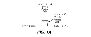
図1Aは、フローティングゲートに電荷を蓄積するEEPROMセルの形をとる不揮発性メモリを概略的に示す。電気的に消去可能でプログラム可能な読み出し専用メモリ(EEPROM)はEPROMに似た構造を持つほか、適度の電圧印加によりフローティングゲートに電荷を電気的に導入、除去するメカニズムを備え、紫外線に晒す必要はない。米国特許第5,595,924号(特許文献6)には、かかるセルの例とその製造方法が記載されている。 FIG. 1A schematically illustrates a non-volatile memory in the form of an EEPROM cell that stores charge in a floating gate. Electrically erasable and programmable read-only memory (EEPROM) has a structure similar to EPROM, and it has a mechanism to electrically introduce and remove charges from the floating gate by applying appropriate voltage, and it must be exposed to ultraviolet rays. There is no. US Pat. No. 5,595,924 (Patent Document 6) describes an example of such a cell and a method for manufacturing the same.
図1Bは、選択ゲートとコントロールゲートまたはステアリングゲートの両方を具備するフラッシュEEPROMセルを概略的に示す。メモリセル10は、ソース14およびドレイン16拡散層間に「スプリットチャネル」12を具備する。セルは、2つの直列トランジスタT1およびT2によって事実上形成される。T1は、フローティングゲート20とコントロールゲート30とを具備するメモリトランジスタとして機能する。フローティングゲートは選択可能な量の電荷を蓄積できる。チャネルのT1部分を流れ得る電流の量は、コントロールゲート30の電圧と、介在するフローティングゲート20に存在する電荷の量とに左右される。T2は、選択ゲート40を具備する選択トランジスタとして機能する。選択ゲート40の電圧によってT2がオンに切り替わると、チャネルのT1部分の電流がソースおよびドレイン間を通過できるようになる。選択トランジスタは、コントロールゲートの電圧から独立したスイッチをソース−ドレインチャネル沿いに提供する。この利点として、フローティングゲートにおける電荷空乏(正)のためにゼロコントロールゲート電圧でなお導通するセルをオフに切り替えることができる。もうひとつの利点として、ソース側の注入プログラミングをより容易に実施できる。
FIG. 1B schematically shows a flash EEPROM cell with both a select gate and a control gate or steering gate. The
図1Bの点線で概略的に示されているように、シンプルなスプリットチャネルメモリセルの実施形態では、選択ゲートとコントロールゲートが同じワード線へ接続される。この場合は、チャネルの一部分に電荷蓄積素子(フローティングゲート)を重ね、他のチャネル部分と電荷蓄積素子にはコントロールゲート構造(ワード線の一部)を重ねる。これにより2つのトランジスタが直列するセルが事実上形成され、一方のトランジスタ(メモリトランジスタ)では、電荷蓄積素子上の電荷量とワード線上の電圧とによりチャネルの当該部分を流れ得る電流の量が制御され、他方のトランジスタ(選択トランジスタ)はゲートとして機能するワード線のみとなる。米国特許第5,070,032号(特許文献7)、第5,095,344号(特許文献8)、第5,315,541号(特許文献9)、第5,343,063号(特許文献10)、および第5,661,053号(特許文献11)には、かかるセルの例と、メモリシステムにおけるその使用と、製造方法とが記載されている。 In the simple split channel memory cell embodiment, the select gate and the control gate are connected to the same word line, as schematically illustrated by the dotted line in FIG. 1B. In this case, a charge storage element (floating gate) is overlaid on a part of the channel, and a control gate structure (a part of a word line) is overlaid on the other channel part and the charge storage element. This effectively forms a cell in which two transistors are in series, and in one transistor (memory transistor), the amount of current that can flow through that portion of the channel is controlled by the amount of charge on the charge storage element and the voltage on the word line. The other transistor (selection transistor) is only the word line functioning as a gate. US Pat. Nos. 5,070,032 (Patent Document 7), 5,095,344 (Patent Document 8), 5,315,541 (Patent Document 9), 5,343,063 (Patent Document) Document 10) and 5,661,053 (Patent Document 11) describe examples of such cells, their use in memory systems, and manufacturing methods.
図1Bに示されたスプリットチャネルセルのより精緻な実施形態では、選択ゲートとコントロールゲートが独立し、点線で結ばれない。一実施例では、ワード線に対して垂直の制御(または、ステアリング)線へ接続されたセルアレイの1列にコントロールゲートを具備する。この場合は、選択されたセルの読み出しやプログラミングにあたって、ワード線が2つの機能を同時に果たさずにすむ。2つの機能とは、(1)選択トランジスタのゲートとして機能すること(そのため、選択トランジスタのオン/オフにあたっては適度の電圧が必要となる)、(2)ワード線と電荷蓄積素子との電界(容量)結合により電荷蓄積素子の電圧を所望のレベルに到達させることである。多くの場合、これらの機能の両方をひとつの電圧で最適に果たすのは困難である。コントロールゲートと選択ゲートの個別制御により、ワード線は機能(1)を果たすだけでよく、機能(2)は追加の制御線が担当する。その結果、対象となるデータにプログラミング電圧を適合させるより高性能なプログラミング設計が可能となる。フラッシュEEPROMアレイにおける独立したコントロール(または、ステアリング)ゲートの使用は、例えば、米国特許第5,313,421号(特許文献12)および第6,222,762号(特許文献13)に記載されている。 In a more elaborate embodiment of the split channel cell shown in FIG. 1B, the select gate and control gate are independent and are not connected by a dotted line. In one embodiment, a control gate is provided in one column of the cell array connected to a control (or steering) line perpendicular to the word line. In this case, the word line does not have to perform two functions at the same time when reading or programming the selected cell. The two functions are (1) functioning as the gate of the selection transistor (so that an appropriate voltage is required to turn on / off the selection transistor), and (2) the electric field between the word line and the charge storage element ( Capacitance) is to bring the voltage of the charge storage element to a desired level. In many cases, it is difficult to optimally perform both of these functions with a single voltage. Due to the individual control of the control gate and select gate, the word line only needs to fulfill function (1), and function (2) is responsible for the additional control line. As a result, a higher-performance programming design that adapts the programming voltage to the target data becomes possible. The use of independent control (or steering) gates in flash EEPROM arrays is described, for example, in US Pat. Nos. 5,313,421 and 6,222,762. Yes.
図1CはもうひとつのフラッシュEEPROMセルを概略的に示すものであり、二重フローティングゲートと、独立した選択ゲートおよびコントロールゲートとを具備する。メモリセル10’は図1Bのメモリセルに類似するが、3つの直列トランジスタを事実上具備する。この種のセルでは、ソースおよびドレイン拡散層間のチャネル上に2つの蓄積素子(すなわち、T1−左とT1−右のもの)があり、その間には選択トランジスタT2がある。このメモリトランジスタはフローティングゲート20’および20’’とコントロールゲート30’および30’’をそれぞれ具備する。選択トランジスタT2は選択ゲート40’によって制御される。読み出しや書き込みにあたっては、常にメモリトランジスタ対のいずれか一方のみにアクセスする。蓄積単位T1−左にアクセスするときにはT2とT1−右の両方がオンになり、チャネルのT1−左部分の電流がソースおよびドレイン間を通過できるようになる。同様に、蓄積単位T1−右にアクセスするときにはT2とT1−左がオンになる。消去にあたっては、選択ゲートポリシリコンの一部分をフローティングゲートに近づけ、選択ゲートに十分な正電圧(例えば、20V)を印加し、フローティングゲートの中に蓄積された電子を選択ゲートポリシリコンへ抜けさせる。
FIG. 1C schematically shows another flash EEPROM cell with a double floating gate and independent select and control gates. Memory cell 10 'is similar to the memory cell of FIG. 1B, but effectively comprises three series transistors. In this type of cell, there are two storage elements (ie, T1-left and T1-right) on the channel between the source and drain diffusion layers, with a select transistor T2 between them. This memory transistor comprises floating
図1Dは、NANDセルの形に構成された一連のメモリセルを概略的に示す。NANDセル50は、ソースおよびドレインによりデイジーチェーン接続された一連のメモリトランジスタM1、M2・・・Mn(n=4,8,16以上)からなる。1対の選択トランジスタS1、S2は、NANDセルのソース端子54とドレイン端子56を通じて外部に至るメモリトランジスタチェーンの接続を制御する。メモリアレイでソース選択トランジスタS1がオンになると、ソース端子がソース線へ結合される。同様に、ドレイン選択トランジスタS2がオンになると、NANDセルのドレイン端子はメモリアレイのビット線へ結合される。チェーンの中の各メモリトランジスタは、一定量の電荷を蓄積して目的の記憶状態を表現する電荷蓄積素子を具備する。読み出し操作と書き込み操作は各メモリトランジスタのコントロールゲートによって制御される。選択トランジスタS1、S2のコントロールゲートはそれぞれ、ソース端子54とドレイン端子56を介したNANDセルへのアクセスを制御する。
FIG. 1D schematically shows a series of memory cells configured in the form of NAND cells. The
NANDセルの中でアドレスされたメモリトランジスタを読み出したりプログラミング中にベリファイしたりするときには、そのコントロールゲートにしかるべき電圧が供給される。同時に、NANDセル50の中でアドレスされない残りのメモリトランジスタは、それぞれのコントロールゲートに印加される十分な電圧により完全にオンになる。こうして個々のメモリトランジスタのソースからNANDセルのソース端子54にかけて導電経路ができあがる。個々のメモリトランジスタのドレインからセルのドレイン端子56についても同様である。米国特許第5,570,315号(特許文献14)、第5,903,495号(特許文献15)、第6,046,935号(特許文献16)には、そのようなNANDセル構造を持つメモリ装置が記載されている。
When a memory transistor addressed in a NAND cell is read or verified during programming, an appropriate voltage is supplied to its control gate. At the same time, the remaining memory transistors that are not addressed in the
図1Eは、誘電体層に電荷を蓄積する不揮発性メモリを概略的に示す。前述した導電性フローティングゲート素子の代わりに誘電体層が使われている。Eitan et al., "NROM: A Novel Localized Trapping, 2-Bit Nonvolatile Memory Cell," IEEE Electron Device Letters, vol. 21, no. 11, November 2000, pp. 543-545(非特許文献1)には、このような誘電性蓄積素子を利用するメモリ装置が記載されている。ソースおよびドレイン拡散層間のチャネルにまたがってONO誘電体層が延在する。1データビットのための電荷はドレインに近い誘電体層に局在し、他のデータビットのための電荷はソースに近い誘電体層に局在する。例えば、米国特許第5,768,192号(特許文献17)および第6,011,725号(特許文献18)には、2つの二酸化ケイ素層にトラッピング誘電体をはさむ不揮発性メモリセルが開示されている。多状態データストレージは、誘電体の中で空間的に隔てられた電荷蓄積領域のバイナリ状態を別々に読み出すことによって実現する。 FIG. 1E schematically illustrates a non-volatile memory that stores charge in a dielectric layer. A dielectric layer is used instead of the conductive floating gate element described above. Eitan et al., "NROM: A Novel Localized Trapping, 2-Bit Nonvolatile Memory Cell," IEEE Electron Device Letters, vol. 21, no. 11, November 2000, pp. 543-545 (Non-Patent Document 1) A memory device using such a dielectric storage element is described. An ONO dielectric layer extends across the channel between the source and drain diffusion layers. The charge for one data bit is localized in the dielectric layer near the drain, and the charge for the other data bit is localized in the dielectric layer near the source. For example, U.S. Pat. Nos. 5,768,192 and 6,011,725 disclose a non-volatile memory cell having a trapping dielectric sandwiched between two silicon dioxide layers. ing. Multi-state data storage is realized by separately reading the binary states of the charge storage regions spatially separated in the dielectric.
メモリアレイ
メモリ装置は通常、行列に配置され、ワード線とビット線によりアドレス可能である二次元メモリセルアレイを備える。アレイはNORタイプかNANDタイプのアーキテクチャに従って形成できる。
Memory array memory devices typically comprise a two-dimensional memory cell array arranged in a matrix and addressable by word lines and bit lines. The array can be formed according to a NOR type or NAND type architecture.
NORアレイ
図2は、NORメモリセルアレイの一例を示す。これまでNORタイプのアーキテクチャを持つメモリ装置は、図1Bまたは図1Cに描かれたタイプのセルを用いて実装されてきた。メモリセル行は、それぞれのソースとドレインによりデイジーチェーン接続される。この設計は仮想接地設計と呼ばれることがある。各々のメモリセル10はソース14と、ドレイン16と、コントロールゲート30と、選択ゲート40とを具備する。行内のセルの選択ゲートはワード線42へ接続する。列内のセルのソースおよびドレインは選択されたビット線34および36へ接続する。メモリセルのコントロールゲートと選択ゲートを別々に制御する一部の実施形態では、ステアリング線36によって列内のセルのコントロールゲートが接続される。
NOR Array FIG. 2 shows an example of a NOR memory cell array. So far, memory devices having a NOR type architecture have been implemented using cells of the type depicted in FIG. 1B or 1C. Memory cell rows are daisy chained by their respective sources and drains. This design is sometimes referred to as a virtual ground design. Each
多くのフラッシュEEPROM装置は、コントロールゲートと選択ゲートがともに接続されたメモリセルによって実装される。この場合、ステアリング線は必要なく、行沿いのセルのコントロールゲートと選択ゲートは全て、ワード線によって単に接続される。米国特許第5,172,338号(特許文献19)および第5,418,752号(特許文献20)には、その設計例が開示されている。この設計で、ワード線は基本的に2つの役割を果たす。つまり、行選択の役割と、読み出しやプログラミングにあたって行内の全セルにコントロールゲート電圧を供給する役割とを果たす。 Many flash EEPROM devices are implemented with memory cells that have a control gate and a select gate connected together. In this case, no steering line is required, and all the control gates and select gates of the cells along the row are simply connected by a word line. U.S. Pat. Nos. 5,172,338 (Patent Document 19) and 5,418,752 (Patent Document 20) disclose design examples. In this design, the word line basically plays two roles. That is, it plays the role of row selection and the role of supplying the control gate voltage to all the cells in the row for reading and programming.
NANDアレイ
図3は、図1Dに見られるメモリセル等からなるNANDアレイの一例を示す。ビット線は各NANDセル列に沿って各NANDセルのドレイン端子56へ結合する。ソース線はNANDセル行に沿って、全ソース端子54へ接続し得る。さらに、行沿いのNANDセルのコントロールゲートは一連の対応するワード線へ接続する。接続されたワード線を通じてコントロールゲートにしかるべき電圧をかけて1対の選択トランジスタ(図1D参照)をオンにすることにより、行全体のNANDセルをアドレスできる。NANDセルのチェーンの中のひとつのメモリトランジスタを読み出すときには、チェーンの中の残りのメモリトランジスタがそれぞれの関連するワード線を通じてハードオンになるため、チェーンの中を流れる電流は、基本的には読み出しの対象となるセルに蓄積される電荷レベルに左右される。米国特許第5,570,315号(特許文献14)、第5,774,397号(特許文献21)、および第6,046,935号(特許文献16)には、NANDアーキテクチャアレイの例とメモリシステムの一部としてのこの動作が記載されている。
NAND Array FIG. 3 shows an example of a NAND array consisting of memory cells and the like seen in FIG. 1D. A bit line is coupled to the
ブロック消去
電荷蓄積メモリ装置のプログラミングではひたすら電荷蓄積素子に電荷が加えられる。このためプログラミング操作にあたっては、電荷蓄積素子に既に存在する電荷を事前に除去(または、消去)しなければならない。1つ以上のメモリセルブロックを消去するため、消去回路(図示せず)を設ける。セルアレイ全体あるいはアレイのかなりのセル群を、電気的に一斉に(すなわち、瞬時に)消去するEEPROM等の不揮発性メモリは「フラッシュ」EEPROMと呼ばれる。消去の後にはセル群を再プログラムできる。一斉に消去できるセル群は1つ以上のアドレス可能な消去単位からなってよい。消去単位またはブロックは通常1ページ以上のデータを蓄積し、このページがプログラミングと読み出しの単位となるが、1回の操作で2ページ以上をプログラムしたり読み出したりする場合もある。各ページには通常1セクタ以上のデータが蓄積され、このセクタのサイズはホストシステムによって決まる。例えば、磁気ディスクドライブの場合は512バイトのユーザデータからなるセクタが標準となり、さらにここにユーザデータおよび/またはこれを蓄積するブロックに関する何バイトかのオーバーヘッド情報が加わる。
In programming the block erase charge storage memory device, a charge is only added to the charge storage element. For this reason, in the programming operation, the charge already existing in the charge storage element must be removed (or erased) in advance. An erase circuit (not shown) is provided to erase one or more memory cell blocks. Non-volatile memory, such as EEPROM, that erases the entire cell array or a substantial group of cells of the array all at once (ie, instantaneously) is called a “flash” EEPROM. The cells can be reprogrammed after erasure. A group of cells that can be erased simultaneously may comprise one or more addressable erase units. An erase unit or block normally stores one or more pages of data, and this page is a unit for programming and reading. However, two or more pages may be programmed or read in one operation. Each page normally stores data of one sector or more, and the size of this sector is determined by the host system. For example, in the case of a magnetic disk drive, a sector consisting of 512-byte user data is standard, and further, several bytes of overhead information relating to user data and / or a block for storing the user data is added thereto.
読み出し/書き込み回路
通常の2状態EEPROMセルでは、1つ以上の電流区切りレベルを設定して伝導ウィンドウを2つの領域に分割する。予め決められた一定の電圧を印加することによってセルを読み出すときには、そのソース/ドレイン電流を区切りレベル(または基準電流IREF)と比較することによって記憶状態を決定する。読み出される電流が区切りレベルの電流より高ければ、セルはひとつの論理状態(例えば「0」状態)にあると判断される。その一方で、電流が区切りレベルの電流に満たなければ、セルはもうひとつの論理状態(例えば、「1」状態)にあると判断される。かかる2状態セルは1ビットのデジタル情報を蓄積する。基準電流源は外部からプログラムでき、通常はメモリシステムの一部として用意され、区切りレベル電流を生成する。
Read / Write Circuit In a normal two-state EEPROM cell, one or more current break levels are set to divide the conduction window into two regions. When reading a cell by applying a predetermined constant voltage, the memory state is determined by comparing its source / drain current with a break level (or reference current I REF ). If the read current is higher than the break level current, the cell is determined to be in one logic state (eg, “0” state). On the other hand, if the current does not reach the break level current, the cell is determined to be in another logic state (eg, “1” state). Such a two-state cell stores 1-bit digital information. The reference current source can be programmed externally and is usually provided as part of the memory system and generates a break level current.
メモリ容量を増やすため、フラッシュEEPROM装置の実装密度は半導体技術の進歩にともないどんどん高くなっている。各メモリセルで3状態以上を蓄積することによって蓄積容量を増やす方法もある。 In order to increase the memory capacity, the mounting density of the flash EEPROM device is increasing with the progress of semiconductor technology. There is also a method of increasing the storage capacity by storing three or more states in each memory cell.
多状態またはマルチレベルのEEPROMメモリセルの場合は、伝導ウィンドウを複数の区切り点で3つ以上の領域に分割し、各セルに2ビット以上のデータを蓄積することができる。つまり所与のEEPROMアレイで蓄積できる情報は、各セルで蓄積できる状態数にともない増加する。米国特許第5,172,338号(特許文献19)には、多状態またはマルチレベルのメモリセルを備えるEEPROMまたはフラッシュEEPROMが記載されている。 In the case of a multi-state or multi-level EEPROM memory cell, the conduction window can be divided into three or more regions at a plurality of break points, and data of 2 bits or more can be stored in each cell. That is, the information that can be stored in a given EEPROM array increases with the number of states that can be stored in each cell. US Pat. No. 5,172,338 describes an EEPROM or flash EEPROM with multi-state or multi-level memory cells.
実際には、コントロールゲートに基準電圧が印加されるときに、セルのソース電極とドレイン電極にかけて伝導電流を検知することによってセルの記憶状態を読み出すのが普通である。つまりセルのフローティングゲート上の所与の各電荷につき、一定の基準コントロールゲート電圧に対して相応の伝導電流を検出できる。同様に、対応するしきい値電圧ウィンドウや対応する伝導電流ウィンドウは、フローティングゲートにプログラムできる電荷の範囲によって決まる。 In practice, when a reference voltage is applied to the control gate, it is common to read the memory state of the cell by sensing the conduction current across the source and drain electrodes of the cell. That is, for each given charge on the cell's floating gate, a corresponding conduction current can be detected for a fixed reference control gate voltage. Similarly, the corresponding threshold voltage window and the corresponding conduction current window are determined by the range of charges that can be programmed into the floating gate.
あるいは、分割された電流ウィンドウの中で伝導電流を検出する代わりに、コントロールゲートで検査の対象となる所与の記憶状態に対してしきい値電圧を設定し、伝導電流がしきい値電流より低いか高いかを検出することも可能である。一実施例において、ビット線のキャパシタンスを通じて放電する伝導電流のレートを調べることによって、しきい値電流に対する伝導電流の検出を果たす。 Alternatively, instead of detecting the conduction current in the divided current window, the control gate sets a threshold voltage for a given memory state to be examined, and the conduction current is less than the threshold current. It is also possible to detect whether it is low or high. In one embodiment, detection of conduction current relative to threshold current is accomplished by examining the rate of conduction current discharging through the bit line capacitance.
図4は、フローティングゲートが常に選択的に蓄積できる4通りの電荷Q1〜Q4におけるソース−ドレイン電流ID とコントロールゲート電圧VCGとの関係を示すものである。実線で描かれた4本のID 対VCG曲線はメモリセルのフローティングゲートにプログラムできる4通りの可能な電荷レベルを表し、4通りの可能な記憶状態にそれぞれ相当する。一例として、セル集団のしきい値電圧ウィンドウは0.5Vから3.5Vにおよび得る。しきい値ウィンドウをそれぞれ0.5Vの間隔で5つの領域に分割することにより、6通りの記憶状態に区切られてよい。例えば、図に示されているように、2μAの基準電流IREF を使用するならば、Q1でプログラムされるセルは、その曲線がVCG=0.5Vおよび1.0Vで区切られたしきい値ウィンドウの領域内でIREF と交差するため、記憶状態「1」にあるとみなされてよい。同様に、Q4は記憶状態「5」にある。 4, a source in the charge Q1~Q4 four kinds of floating gate can always selectively accumulate - shows the relationship between the drain current I D and the control gate voltage V CG. The four I D vs. V CG curves drawn with solid lines represent the four possible charge levels that can be programmed into the floating gate of the memory cell, each corresponding to four possible storage states. As an example, the threshold voltage window of the cell population can range from 0.5V to 3.5V. The threshold window may be divided into five storage states by dividing each threshold window into five regions at intervals of 0.5V. For example, as shown in the figure, if a 2 μA reference current I REF is used, a cell programmed with Q1 has a threshold whose curve is separated by V CG = 0.5V and 1.0V. Since it crosses I REF within the region of the value window, it may be considered to be in the memory state “1”. Similarly, Q4 is in the storage state “5”.
前の説明から分かるように、メモリセルで蓄積する状態が多ければ多いほどしきい値ウィンドウは細かく分割される。そこで所要の分解能を達成するには、プログラミング操作と読み出し操作の精度を上げる必要がある。 As can be seen from the previous description, the threshold value window is divided more finely as more states are accumulated in the memory cell. Therefore, to achieve the required resolution, it is necessary to improve the accuracy of the programming operation and the reading operation.
米国特許第4,357,685号(特許文献22)には2状態EPROMをプログラムする方法が開示され、この方法では、所与の状態までセルがプログラムされると、セルが相継ぐプログラミング電圧パルスに晒され、そのつどフローティングゲートに電荷が加わる。パルスの合間にはセルのリードバックまたはベリファイを行い、区切りレベルに対するソース−ドレイン電流を確認する。所望の状態に達した電流が確認されるとプログラミングは停止する。使用するプログラミングパルストレインの周期または振幅は上げることができる。 U.S. Pat. No. 4,357,685 discloses a method for programming a two-state EPROM, where the programming voltage pulse that the cell inherits once the cell is programmed to a given state. Each time, the floating gate is charged. The cell is read back or verified between pulses, and the source-drain current with respect to the break level is confirmed. Programming is stopped when the current reaching the desired state is confirmed. The period or amplitude of the programming pulse train used can be increased.
先行技術のプログラミング回路では、消去または接地状態から目標状態に達するまでプログラミングパルスを単に印加しながらしきい値ウィンドウを通過していく。実際面で十分な分解能を実現するには、分割されたかあるいは区切られた各領域につき、最低でも5ステップ程度のプログラミングステップを踏む必要がある。2状態メモリセルならば、性能は許容される。しかし、多状態セルの場合は、必要ステップ数が分割数にともない増加するため、プログラミングの精度または分解能を上げなければならない。例えば、16状態セルで目標状態までプログラムするには、最低でも平均40のプログラミングパルスが必要となる。 In prior art programming circuits, the programming window simply passes through the threshold window until it reaches the target state from the erase or ground state. In order to achieve a sufficient resolution in practice, it is necessary to perform programming steps of at least about 5 steps for each divided or divided area. With a two-state memory cell, performance is acceptable. However, in the case of a multi-state cell, the number of required steps increases with the number of divisions, so the programming accuracy or resolution must be increased. For example, programming to a target state with a 16 state cell requires an average of 40 programming pulses at a minimum.
図5は、読み出し/書き込み回路170から行デコーダ130と列デコーダ160とを通じて典型的なメモリアレイ構成100にアクセスするメモリ装置を概略的に示す。図2および図3に関連して説明したように、メモリアレイ100の中にあるメモリセルのメモリトランジスタは、1組の選択されたワード線とビット線を通じてアドレスできる。アドレスされたメモリトランジスタのそれぞれのゲートにしかるべき電圧を印加するため、行デコーダ130は1つ以上のワード線を選択し、列デコーダ160は1つ以上のビット線を選択する。読み出し/書き込み回路170は、アドレスされたメモリトランジスタの記憶状態を読み出すかまたは書き込む(プログラムする)ためにある。読み出し/書き込み回路170は、ビット線を通じてアレイ内の記憶素子へ接続可能ないくつかの読み出し/書き込みモジュールを備える。
FIG. 5 schematically illustrates a memory device that accesses a typical
図6Aは、個々の読み出し/書き込みモジュール190の概略的ブロック図である。読み出しやベリファイのときには基本的に、選択されたビット線を通じて接続するアドレスされたメモリトランジスタのドレインを流れる電流をセンスアンプで判定する。この電流は、メモリトランジスタに蓄積された電荷とそのコントロールゲート電圧に左右される。例えば、多状態EEPROMセルでは、数通りのレベルのいずれかまでフローティングゲートを荷電できる。これにより、4レベルセルならば、2ビットのデータを蓄積できる。センスアンプによって検出されたレベルはレベル−ビット変換ロジックによって1組のデータビットに変換され、データラッチに蓄積される。
FIG. 6A is a schematic block diagram of an individual read /
読み出し/書き込み性能・精度に影響する要因
読み出しとプログラミングの性能を上げるには、アレイの中にある複数の電荷蓄積素子またはメモリトランジスタを並行して読み出すかまたはプログラムする。つまり、記憶素子からなる論理「ページ」の読み出しまたはプログラミングは一斉に行われる。既存のメモリアーキテクチャでは通常、1行の中にいくつかの交互ページがある。読み出しまたはプログラミングは1ページの全記憶素子で一斉に行われる。列デコーダは交互ページの各々を対応する数の読み出し/書き込みモジュールへ選択的に接続する。例えば、一実施例において、532バイト(512バイトにオーバーヘッドの20バイトを加えたもの)のページサイズでメモリアレイを設計する。各列にドレインビット線があって各行につき2つの交互ページがあるならば、列は8,512列になり、各ページに4,256列が対応する。全ての偶数ビット線か奇数ビット線を並行して読み書きするには、4,256個のセンスモジュールを接続することになる。こうして、記憶素子のページには1ページ4,256ビット(すなわち、532バイト)のデータを並行して読み出すかまたはプログラムする。読み出し/書き込み回路170を形成する読み出し/書き込みモジュールは、様々なアーキテクチャに組むことができる。
Factors Affecting Read / Write Performance / Accuracy To improve read and programming performance, multiple charge storage elements or memory transistors in the array are read or programmed in parallel. That is, reading or programming of logical “pages” made up of storage elements is performed all at once. Existing memory architectures typically have several alternating pages in a row. Reading or programming is performed simultaneously on all memory elements of one page. A column decoder selectively connects each of the alternating pages to a corresponding number of read / write modules. For example, in one embodiment, a memory array is designed with a page size of 532 bytes (512 bytes plus 20 bytes of overhead). If there is a drain bit line in each column and there are two alternating pages per row, the column will be 8,512 columns, with 4,256 columns corresponding to each page. To read / write all even bit lines or odd bit lines in parallel, 4,256 sense modules are connected. Thus, the page of the memory element is read or programmed in parallel with 4 pages of 256 bits (that is, 532 bytes). The read / write module forming the read /
図5を参照すると、読み出し/書き込み回路170は、数バンクの読み出し/書き込みスタック180に編制されている。それぞれの読み出し/書き込みスタック180は読み出し/書き込みモジュール190を積み重ねたものである。メモリアレイにおける列の間隔は、これを占有する1つまたは2つのトランジスタのサイズによって決まる。しかし、図6Aから見てとれるように、読み出し/書き込みモジュールの回路はさらに多くのトランジスタと回路素子により実装され、多数の列にわたってスペースを占めることが見込まれる。占有された列の中で2つ以上の列を処理するため、多数のモジュールを互いに積み重ねる。
Referring to FIG. 5, the read /
図6Bは、読み出し/書き込みモジュール190の積み重ねにより従来どおりに実装された図5の読み出し/書き込みスタックを示す。例えば、読み出し/書き込みモジュールが16列にわたって延在するならば、1スタックに8読み出し/書き込みモジュールの読み出し/書き込みスタック180により8列を並列処理できる。この読み出し/書き込みスタックは列デコーダを通じて、バンク中の8つの奇数(1,3,5,7,9,11,13,15)列か8つの偶数(2,4,6,8,10,12,14,16)列に結合できる。
FIG. 6B shows the read / write stack of FIG. 5 implemented conventionally by stacking read /
既に述べたように、従来のメモリ装置は一度に全ての偶数ビット線か全ての奇数ビット線に対して大規模な並列処理を行うことによって、読み出し/書き込み操作を向上させる。この1行2交互ページのアーキテクチャは、読み出し/書き込み回路ブロックの整合問題の緩和に役立つ。これはビット線間容量結合をいかにコントロールするかにも左右される。1組の読み出し/書き込みモジュールを偶数ページか奇数ページに多重化するには、ブロックデコーダを使用する。こうすることで、1組のビット線で読み出しかプログラミングが行われているときには常に、互い違いのビット線を接地でき、近傍結合は最小限に抑えられる。 As already mentioned, conventional memory devices improve read / write operations by performing massively parallel processing on all even bit lines or all odd bit lines at once. This one-row, two-alternate page architecture helps mitigate read / write circuit block alignment problems. This also depends on how to control the capacitive coupling between the bit lines. A block decoder is used to multiplex a set of read / write modules into even or odd pages. In this way, alternate bit lines can be grounded whenever read or programming is performed on a set of bit lines, and neighborhood coupling is minimized.
しかし、交互ページアーキテクチャは少なくとも3つの点で不利である。第1に、追加の多重化回路が必要となる。第2に、動作が遅い。ワード線によって接続されたメモリセルあるいは1行のメモリセルで、読み出しまたはプログラミングを完了するには、2回の読み出し操作か2回のプログラミング操作が必要となる。第3に、2つの近傍電荷蓄積素子が別々のときにプログラムされる、例えば奇数ページと偶数ページとで別々にプログラムされる場合のフローティングゲートレベルにおける近傍電荷蓄積素子間の電界結合等、他の好ましくない影響に対処するにあたって最適ではない。 However, the alternating page architecture is disadvantageous in at least three respects. First, an additional multiplexing circuit is required. Second, it is slow. In order to complete reading or programming in a memory cell connected by a word line or one row of memory cells, two read operations or two programming operations are required. Third, the two neighboring charge storage elements are programmed when they are separated, for example, electric field coupling between neighboring charge storage elements at the floating gate level when programmed separately for odd pages and even pages, etc. It is not optimal in dealing with undesirable effects.
近傍電界結合の問題はメモリトランジスタの間隔が狭まるにつれて顕著となる。メモリトランジスタでは、チャネル領域とコントロールゲートの間に電荷蓄積素子が挟まれている。チャネル領域を流れる電流は、電荷蓄積素子とコントロールゲートの電界によって生じる最終的な電界に相関する。メモリトランジスタは密度の増加にともない互いに接近する。近傍電荷素子からの電界は、影響を受けるセルの最終的な電界に大きく寄与する。近傍の電界は、近傍の電荷蓄積素子にプログラムされる電荷に左右される。この摂動を招く電界には、近傍電荷蓄積素子のプログラム状態に応じて変化する動的な性質がある。近傍電荷蓄積素子の状態の変化によっては、影響を受けるセルの読み出しに時間によってばらつきが生じるおそれがある。 The problem of near-field coupling becomes more prominent as the memory transistor spacing decreases. In a memory transistor, a charge storage element is sandwiched between a channel region and a control gate. The current flowing through the channel region correlates with the final electric field generated by the electric field of the charge storage element and the control gate. Memory transistors approach each other with increasing density. The electric field from the nearby charge device greatly contributes to the final electric field of the affected cell. The nearby electric field depends on the charge programmed into the nearby charge storage element. The electric field that causes this perturbation has a dynamic property that changes according to the program state of the nearby charge storage element. Depending on the change in the state of the neighboring charge storage element, there is a possibility that the reading of the affected cell may vary with time.
従来の交互ページアーキテクチャでは、近傍フローティングゲート結合によって生じるエラーが激化する。プログラミングと読み出しは偶数ページと奇数ページで別々に行われるため、介在するページの状況次第では、ページがプログラムされるときの1組の条件とページの読み返しが行われるときの1組の条件がまったく異なることがある。読み出しエラーは密度の増加にともない深刻化するため、多状態の実施例では、読み出し操作の精度を上げてしきい値ウィンドウの分割を粗くする必要がある。性能は損なわれ、多状態の実施例での潜在的キャパシティは制限される。 Conventional alternating page architectures exacerbate errors caused by neighboring floating gate coupling. Since programming and reading are performed separately for even and odd pages, depending on the status of the intervening page, there is exactly one set of conditions when the page is programmed and one set of conditions when the page is read back. May be different. Since read errors become more serious with increasing density, in multi-state embodiments, it is necessary to increase the accuracy of the read operation and coarsen the threshold window division. Performance is compromised and the potential capacity in multi-state embodiments is limited.
米国公開特許出願第2004−0060031号(特許文献23)には、大きな読み出し/書き込み回路ブロックで相応のメモリセルブロックを並行して読み書きする、高性能でありながらコンパクトな不揮発性メモリ装置が開示されている。特にこのメモリ装置のアーキテクチャは、読み出し/書き込み回路ブロックの無駄を最小限に抑える。時分割方式で少数の共通部分とやり取りしながら並行して作動するブロック読み出し/書き込みモジュールの中核部分に読み出し/書き込みモジュールブロックを再配分することにより、スペースと電力を大幅に節約する。特に、読み出し/書き込み回路の複数のセンスアンプおよびデータラッチ間のデータ処理は共通のプロセッサによって実行される。 US Published Patent Application No. 2004-0060031 (Patent Document 23) discloses a high-performance but compact non-volatile memory device that reads and writes a corresponding memory cell block in parallel with a large read / write circuit block. ing. In particular, this memory device architecture minimizes the waste of read / write circuit blocks. By redistributing the read / write module blocks to the core part of the block read / write module that operates in parallel while interacting with a small number of common parts in a time-sharing manner, it saves significant space and power. In particular, data processing between a plurality of sense amplifiers and data latches of the read / write circuit is executed by a common processor.
このように高性能・大容量不揮発性メモリが一般に求められている。特に、読み出しとプログラミングの性能が高く、コンパクトで効率的でありながら読み出し/書き込み回路におけるデータ処理に幅広く対応する改良されたプロセッサを備えるコンパクトな不揮発性メモリが求められている。 Thus, there is a general demand for high performance and large capacity nonvolatile memories. In particular, there is a need for a compact non-volatile memory with an improved processor that has high read and programming performance, is compact and efficient, but supports a wide range of data processing in read / write circuits.
本発明の一態様によると、メモリページ内データのランダム化により、複数のページでデータが並ぶ場合でも、プログラミング中に問題となるデータパターンは回避される。
好適な実施形態において、ページ上でデータをスクランブルするシンプルな方法により、データはページごとに独立しているかまたは異なる開始アドレスに書き込まれる。メモリセルの各ページには、ページごとに異なる開始位置に対応するデータページが書き込まれる。ページの終わりまでデータで埋め尽くされると、ページの最初のアドレスからラップアラウンドし、開始位置の手前まで書き込みを継続する。
別の好適な実施形態では、擬似ランダムジェネレータによって一連の開始物理列アドレスが各ページにつき1つずつ提供される。
According to one aspect of the present invention, randomization of data in a memory page avoids a data pattern that becomes a problem during programming even when data is arranged in a plurality of pages.
In the preferred embodiment, the data is written to each page independently or at a different starting address by a simple method of scrambling the data on the page. Each page of memory cells is written with a data page corresponding to a different start position for each page. When it is filled with data to the end of the page, it wraps around from the first address of the page and continues to write until the start position.
In another preferred embodiment, a series of starting physical column addresses are provided, one for each page, by a pseudo-random generator.
本発明の別の態様によると、ページに含まれる消去済み状態とプログラム済み状態のセルの割合が平均して等しくなるように、ページ内のデータビットがランダム化される。これによりソース線バイアスまたは負荷の大きなばらつきを抑え、検知操作中のしかるべき調整により許容できるようにする。
それには、ページ内の個々のビットをランダム化する。好ましくは、それぞれ特定の極性を指定する一連の擬似ランダムビットを使ってページ内のビットを符号化する。一実施形態において、ページ内の各データビットにつき極性ビットがある。別の実施形態では、ページ内の各データバイトにつき極性ビットがある。この実施形態で、極性ビットによってビットの反転が指定される場合は、データバイト内の全ビットが反転される。
According to another aspect of the invention, the data bits in the page are randomized such that the proportion of erased and programmed cells contained in the page are equal on average. This suppresses large variations in source line bias or load so that it can be tolerated by appropriate adjustments during the sensing operation.
This is done by randomizing the individual bits in the page. Preferably, the bits in the page are encoded using a series of pseudo-random bits each specifying a particular polarity. In one embodiment, there is a polarity bit for each data bit in the page. In another embodiment, there is a polarity bit for each data byte in the page. In this embodiment, when bit inversion is specified by the polarity bit, all bits in the data byte are inverted.
本発明のもうひとつの態様によると、ページ内ランダム化にページ単位のランダム化を組み合わせる。具体的にはオンチップ回路の限りあるリソースを踏まえ、ページ内ランダム化にあたっては各ページに個別の開始位置を用意するのが望ましく、ページ単位ランダム化にあたっては各ページに個別の符号化極性を用意するのが望ましい。
別の実施形態では、各ページに個別の開始位置を用意するページ内ランダム化に加えて、ページ内の各データビットセットに個別の符号化極性を用意する。
According to another aspect of the present invention, page-by-page randomization is combined with intra-page randomization. Specifically, based on the limited resources of the on-chip circuit, it is desirable to prepare a separate start position for each page for randomization within a page, and a separate encoding polarity for each page for randomization by page. It is desirable to do.
In another embodiment, in addition to intra-page randomization that provides a separate starting position for each page, a separate encoding polarity is provided for each data bit set within the page.
種々のランダム化手法と実施形態はメモリチップ(EEPROM)で実施される。つまり、チップと通信するメモリコントローラによって実施されるのではなく、メモリチップ自体の中で実施される。これはウェアレベリングと呼ばれる問題対処法とは異なる。この手法は主にシステムレベルで実施され、コントローラを使ってメモリチップにおけるデータ蓄積のあり方を変更する。
本発明は、プログラムディスターブやユーザリードディスターブの原因となる特定のデータパターンを軽減もしくは解消するほか、NANDストリング抵抗効果を抑え、メモリの耐久性と信頼性を高める。フローティングゲート間結合の問題も緩和する。
Various randomization techniques and embodiments are implemented in a memory chip (EEPROM). That is, it is not implemented by a memory controller that communicates with the chip, but within the memory chip itself. This is different from a problem-handling method called wear leveling. This method is mainly implemented at the system level, and uses a controller to change the way data is stored in the memory chip.
The present invention reduces or eliminates specific data patterns that cause program disturb and user read disturb, suppresses the NAND string resistance effect, and improves the durability and reliability of the memory. The problem of coupling between floating gates is alleviated.
図7A〜図20は、本発明を実装する好適なメモリシステムを示す。
図7Aは、1バンクの分割読み出し/書き込みスタックを有するコンパクトなメモリ装置を概略的に示すものであり、ここに本発明の改良されたプロセッサが実装される。このメモリ装置は、二次元のメモリセルアレイ300と、制御回路310と、読み出し/書き込み回路370とを備える。メモリアレイ300は、行デコーダ330によりワード線ごとにアドレスでき、列デコーダ360によりビット線ごとにアドレスできる。読み出し/書き込み回路370は1バンクの分割読み出し/書き込みスタック400として実装され、メモリセルからなるブロック(「ページ」とも呼ばれる)の読み出しまたはプログラミングを並行して行うことができる。好適な実施形態において、ページは一連のメモリセル行から構成される。1行のメモリセルを多数のブロックまたはページに分割する別の実施形態において、個々のブロックに向けて読み出し/書き込み回路370を多重化するためにブロックマルチプレクサ350を設ける。
7A-20 illustrate a preferred memory system implementing the present invention.
FIG. 7A schematically illustrates a compact memory device having a bank of split read / write stacks in which the improved processor of the present invention is implemented. The memory device includes a two-dimensional
制御回路310は、読み出し/書き込み回路370と協働しながらメモリアレイ300でメモリ操作を遂行する。制御回路310は、状態マシン312と、オンチップアドレスデコーダ314と、電力制御モジュール316とを備える。状態マシン312はチップレベルのメモリ動作制御を行う。オンチップアドレスデコーダ314は、ホストまたはメモリコントローラで使われるアドレスからデコーダ330および370で使われるハードウェアアドレスへのアドレスインターフェイスを提供する。電力制御モジュール316は、メモリ操作中にワード線とビット線へ供給される電力と電圧を制御する。
The
図7Bは、図7Aに示されたコンパクトなメモリ装置の好適な構成を示す。様々な周辺回路によるメモリアレイ300へのアクセスは、アレイの両側で相称的に行われるため、アクセス線と回路はそれぞれの側で半々になる。つまり、行デコーダは行デコーダ330Aおよび330Bに分かれ、列デコーダは列デコーダ360Aおよび360Bに分かれる。メモリセル行を多数のブロックに分割する実施形態では、ブロックマルチプレクサ350がブロックマルチプレクサ350Aおよび350Bに分かれる。同様に、読み出し/書き込み回路は、アレイ300の下からビット線へ接続する読み出し/書き込み回路370Aと、アレイ300の上からビット線へ接続する読み出し/書き込み回路370Bとに分かれる。このように、読み出し/書き込みモジュールの密度と分割読み出し/書き込みスタック400の密度は、基本的に2分の1になる。
FIG. 7B shows a preferred configuration of the compact memory device shown in FIG. 7A. Since access to the
図8は、図7Aに示された読み出し/書き込みスタックにおける基本コンポーネントの一般的な構成を概略的に示す。本発明の一般的なアーキテクチャによると、読み出し/書き込みスタック400は、k本のビット線を検知する1スタックのセンスアンプ212と、I/Oバス231経由でデータを入出力するI/Oモジュール440と、入出力データを蓄積する1スタックのデータラッチ430と、読み出し/書き込みスタック400でデータを処理し蓄積する共通プロセッサ500と、スタックコンポーネントの通信用スタックバス421とを備える。読み出し/書き込みスタック370内の種々のコンポーネントを制御するため、読み出し/書き込みスタックのスタックバスコントローラから線411を通じて制御信号とタイミング信号が提供される。
FIG. 8 schematically illustrates the general configuration of the basic components in the read / write stack shown in FIG. 7A. According to the general architecture of the present invention, the read /
図9は、図7Aおよび図7Bに示された読み出し/書き込み回路における読み出し/書き込みスタックの好適な一構成を示す。各々の読み出し/書き込みスタック400は、k本のビット線群に同時に働きかける。1ページのビット線がp=r*kなら、r個の読み出し/書き込みスタック400−1,・・・,400−rがある。
分割読み出し/書き込みスタック400からなるバンク全体が並行して作動することにより、行沿いにp個のセルからなるブロック(またはページ)の読み出しまたはプログラミングを並行して行うことができる。この場合は、セル行全体に対してp個の読み出し/書き込みモジュールが存在することになる。各スタックでk個のメモリセルを処理するならば、バンク内の合計読み出し/書き込みスタック数はr=p/kで求められる。例えば、バンク内のスタック数がrならば、p=r*kである。例えば、メモリアレイにおいてk=8、r=512ならば、p=512バイト(512×8ビット)となる。ブロックは、好適な実施形態において、セル行全体である。ブロックは、別の実施形態において、行内のセルの小集団である。セルの小集団とは、例えば行全体の2分の1であったり、行全体の4分の1であったりする。セルの小集団は連続するセルであったり、1つおきのセルであったり、一定セル数おきのセルである。
FIG. 9 shows a preferred configuration of the read / write stack in the read / write circuit shown in FIGS. 7A and 7B. Each read /
By operating the entire bank of split read /
それぞれの読み出し/書き込みスタック、例えば400−1の中には、基本的にk個のメモリセルからなるセグメントを並行して処理する1スタックのセンスアンプ212−1から212−kがある。その全体が本願明細書において参照により援用されている米国公開特許出願第2004−0109357号(特許文献24)には、好適なセンスアンプが開示されている。
スタックバスコントローラ410は、線411を通じて読み出し/書き込み回路370へ制御信号とタイミング信号を提供する。スタックバスコントローラ自体は、線311を通じてメモリコントローラ310に従属する。各読み出し/書き込みスタック400内の通信は相互接続スタックバス421(図8参照)によって行われ、スタックバスコントローラ410によって制御される。制御線411は、スタックバスコントローラ410から読み出し/書き込みスタック400−1のコンポーネントへ制御信号とクロック信号を提供する。
Within each read / write stack, for example 400-1, there is one stack of sense amplifiers 212-1 to 212-k that processes segments of k memory cells in parallel. A suitable sense amplifier is disclosed in U.S. Published Patent Application No. 2004-0109357, which is incorporated herein by reference in its entirety.
スタックバスは、好適な構成において、共通プロセッサ500とセンスアンプ212のスタックとの通信のためのSAバス422と、プロセッサとデータラッチ430のスタックとの通信のためのDバス423とに分かれる。
データラッチ430のスタックには、当該スタックに対応する各メモリセルにつき1つずつ、430−1から430−kまでのデータラッチがある。I/Oモジュール440は、データラッチがI/Oバス231を通じて外部とデータをやり取りできるようにする。 共通プロセッサはまた、エラー状態等、メモリの動作状態を伝えるステータス信号を出力する出力507を含む。このステータス信号は、Wired−OR構成でフラグバス509へ結合されたn−トランジスタ550のゲートを駆動するために使われる。フラグバスは、好ましくはコントローラ310によって予め荷電され、いずれかの読み出し/書き込みスタックによってステータス信号がアサートされるとプルダウンされる。
In a preferred configuration, the stack bus is divided into an
In the stack of data latches 430, there are data latches 430-1 to 430-k, one for each memory cell corresponding to the stack. The I /
図10は、図9に示された共通プロセッサの改良された実施形態を示す。共通プロセッサ500は、外部回路との通信のためのプロセッサバスPバス505と、入力ロジック510と、プロセッサラッチPラッチ520と、出力ロジック530とを備える。
入力ロジック510はPバスからデータを受信し、スタックバスコントローラ410から信号線411経由で届く制御信号に応じて論理状態「1」、「0」、または「Z」(フローティング)のいずれかひとつに変換されるデータとして、BSIノードへ出力する。次に、セット/リセットラッチであるPラッチ520がBSIをラッチすることで、MTCHおよびMTCH*として一対の相補出力信号が用意される。
出力ロジック530はMTCH信号とMTCH*信号を受信し、スタックバスコントローラ410から信号線411経由で届く制御信号に応じて論理状態「1」、「0」、または「Z」(フローティング)のいずれかひとつに変換されるデータを、Pバス505沿いに出力する。
FIG. 10 shows an improved embodiment of the common processor shown in FIG. The
The
The
共通プロセッサ500は特定のメモリセルに関係するデータを常に処理する。例えば、図10は、メモリセルがビット線1へ結合される場合を示している。対応するセンスアンプ212−1のノードにはセンスアンプデータが出現する。このノードは好適な実施形態において、SAラッチ214−1の形をとり、データを蓄積する。同様に、ビット線1へ結合されたメモリセルに関連する入力または出力データは、対応する1セットのデータラッチ430−1に蓄積される。1セットのデータラッチ430−1は、好適な実施形態において、nビットのデータを蓄積するにあたって十分なデータラッチ434−1・・・434−nを備える。
The
共通プロセッサ500のPバス505は、一対の相補信号SAPおよびSANによって転送ゲート501がイネーブルされると、Sバス422経由でSAラッチ214−1に到達する。同様に、一対の相補信号DTPおよびDTNによって転送ゲート502がイネーブルされると、Pバス505からDバス423経由で1セットのデータラッチ430−1に到達する。信号SAP、SAN、DTP、およびDTNは、スタックバスコントローラ410からの制御信号の一部として明示されている。
The
図11Aは、図10に示された共通プロセッサの入力ロジックの好適な実施形態を示す。入力ロジック520はPバス505沿いにデータを受信し、制御信号に応じて出力BSIは同じになるか、反転するか、フローティングする。出力BSIノードは基本的に、Vddにかけて直列するpトランジスタ524および525を備えるプルアップ回路か、接地にかけて直列するnトランジスタ526および527を備えるプルダウン回路か、転送ゲート522の出力に左右される。プルアップ回路のpトランジスタ524および525へ至るゲートは、信号PBUSおよびONEによってそれぞれ制御される。プルダウン回路のnトランジスタ526および527へ至るゲートは、信号ONEB<1>およびPBUSによってそれぞれ制御される。
FIG. 11A shows a preferred embodiment of the input logic of the common processor shown in FIG. The
図11Bは、図11Aの入力ロジックの真理値表を示す。このロジックは、PBUSと制御信号ONE、ONEB<0>、ONEB<1>とによって制御される。これらの制御信号はスタックバスコントローラ410からの制御信号の一部である。基本的には3つの転送モードPASSTHROUGH、INVERTED、およびFLOATEDをサポートする。
BSIが入力データと同じになるPASSTHROUGHモードの場合、信号ONEは論理「1」、ONEB<0>は「0」、ONEB<1>は「0」となる。これによりプルアップまたはプルダウンはディスエーブルされるが、転送ゲート522はイネーブルされ、データはPバス505に沿って出力523へ引き渡される。BSIが入力データの逆になるINVERTEDモードの場合、信号ONEは「0」、ONEB<0>は「1」、ONEB<1>は「1」となる。これにより、転送ゲート522はディスエーブルされる。また、PBUSが「0」ならプルダウン回路はディスエーブルされ、プルアップ回路はイネーブルされ、結果的にBSIは「1」になる。同様に、PBUSが「1」ならば、プルアップ回路はディスエーブルされ、プルダウン回路はイネーブルされ、結果的にBSIは「0」になる。最後に、FLOATEDモードの場合は、信号ONEが「1」、ONEB<0>が「1」、ONEB<1>が「0」となり、出力BSIをフローティングさせることができる。FLOATEDモードは完全を期するために記載されているが、実際には使われない。
FIG. 11B shows a truth table for the input logic of FIG. 11A. This logic is controlled by PBUS and control signals ONE, ONEB <0>, ONEB <1>. These control signals are part of the control signals from the
In the PASSTHROUGH mode in which the BSI is the same as the input data, the signal ONE is logic “1”, the ONEB <0> is “0”, and the ONEB <1> is “0”. This disables pull-up or pull-down, but enables the
図12Aは、図10に示された共通プロセッサの出力ロジックの好適な実施形態を示す。入力ロジック520からBSIノードに至る信号はプロセッサラッチ、Pラッチ520でラッチされる。出力ロジック530はPラッチ520の出力からデータMTCHおよびMTCH*を受信し、制御信号に応じてPASSTHROUGHモードか、INVERTEDモードか、FLOATEDモードでPバス沿いに出力する。換言すると、4本のブランチはPバス505の駆動部として機能し、これをHIGH、LOW、またはFLOATED状態まで能動的に引き上げる。これは、Pバス505の4つのブランチ回路、具体的には2つのプルアップ回路と2つのプルダウン回路とによって果たされる。第1のプルアップ回路はVddにかけて直列するpトランジスタ531および532を備え、MTCHが「0」のときにPバスをプルアップできる。第2のプルアップ回路は接地にかけて直列するpトランジスタ533および534を備え、MTCHが「1」のときにPバスをプルアップできる。同様に、第1のプルダウン回路はVddにかけて直列するnトランジスタ535および536を備え、MTCHが「0」のときにPバスをプルダウンできる。第2のプルアップ回路は接地にかけて直列するnトランジスタ537および538を備え、MTCHが「1」のときにPバスをプルアップできる。
FIG. 12A shows a preferred embodiment of the output logic of the common processor shown in FIG. A signal from the
本発明の一特徴として、プルアップ回路はPMOSトランジスタで構成され、プルダウン回路はNMOSトランジスタで構成される。NMOSによるプルはPMOSのプルより遥かに強いため、競合する場合は常にプルダウンがプルアップに勝る。換言すると、ノードまたはバスはデフォルトとして常にプルアップまたは「1」状態にでき、必要とあらば常にプルダウンにより「0」状態に反転させることができる。 As one feature of the present invention, the pull-up circuit is composed of a PMOS transistor, and the pull-down circuit is composed of an NMOS transistor. Since pulling by NMOS is much stronger than pulling by PMOS, pull-down always wins over pull-up when competing. In other words, a node or bus can always be pulled up or "1" as a default, and can be inverted to a "0" state by pulldown whenever necessary.
図12Bは、図12Aの出力ロジックの真理値表を示す。このロジックは、入力ロジックからラッチされるMTCH、MTCH*と、制御信号PDIR、PINV、NDIR、NINVとによって制御される。これらの制御信号はスタックバスコントローラ410からの制御信号の一部である。4つの動作モード、PASSTHROUGH、INVERTED、FLOATED、およびPRECHARGEをサポートする。
FIG. 12B shows a truth table for the output logic of FIG. 12A. This logic is controlled by MTCH and MTCH * latched from the input logic and control signals PDIR, PINV, NDIR and NINV. These control signals are part of the control signals from the
FLOATEDモードでは4本のブランチがすべてディスエーブルになる。これは信号、PINV=1、NINV=0、PDIR=1、NDIR=0によって達成される。これらはデフォルト値でもある。PASSTHROUGHモードでMTCH=0ならば、PBUS=0が要求される。それにはnトランジスタ535および536を備えるプルダウンブランチだけをイネーブルし、NDIR=1を除き、制御信号はどれもデフォルト値とする。MTCH=1ならば、PBUS=1が要求される。それにはpトランジスタ533および534を備えるプルアップブランチだけをイネーブルし、PINV=0を除き、制御信号はどれもデフォルト値とする。INVERTEDモードでMTCH=0ならば、PBUS=1が要求される。それにはpトランジスタ531および532を備えるプルアップブランチだけをイネーブルし、PDIR=0を除き、制御信号はどれもデフォルト値とする。MTCH=1ならば、PBUS=0が要求される。それにはnトランジスタ537および538を備えるプルダウンブランチだけをイネーブルし、NINV=1を除き、制御信号はどれもデフォルト値とする。PRECHARGEモードでは、PDIR=0とPINV=0の制御信号設定でMTCH=1ならば、pトランジスタ531および531を備えるプルアップブランチがイネーブルされ、MTCH=0ならば、pトランジスタ533および534を備えるプルアップブランチがイネーブルされる。
その全体が本願明細書において参照により援用されている米国公開特許出願第2006−0140007号(特許文献25)では、共通プロセッサの動作がより詳しく説明されている。
In FLOATED mode, all four branches are disabled. This is achieved by the signals PINV = 1, NINV = 0, PDIR = 1, NDIR = 0. These are also default values. If MTCH = 0 in PASSTHROUGH mode, PBUS = 0 is required. To do this, only the pull-down branch with n-
US Published Patent Application No. 2006-0140007, which is incorporated by reference herein in its entirety, describes the operation of the common processor in more detail.
キャッシュ操作におけるデータラッチの使用
本発明のいくつかの態様において、読み出し、書き込み、消去といったほかの作業に内部メモリが従事しているときにデータを出し入れするキャッシュ操作にあたって、図10で前述した読み出し/書き込みスタックのデータラッチを利用する。前述したアーキテクチャでは、多数の物理ページによってデータラッチが共用される。例えば、ビット線の読み出し/書き込みスタックを全てのワード線で共用すれば、あるひとつの操作が進行しているときに空いているラッチがあれば、同じワード線か別のワード線における先々の操作に向けて空いているラッチにデータをキャッシュできるため、転送時間は他の操作の背後に潜在化され、時間の節約になる。この場合は異なる操作または操作段階のパイプライン処理の拡大により性能を上げることができる。例えば、キャッシュプログラミング操作で1ページのデータをプログラムしているときに別のページのデータを読み込めば、転送時間を節約できる。他の例として、例示的な実施形態において、あるひとつのワード線における読み出し操作を別のワード線における書き込み操作に挿入することにより、データの書き込みを継続しながら読み出しデータをメモリから出すことができる。
Use of Data Latches in Cache Operations In some aspects of the invention, the read / write operation described above in FIG. Use the data stack of the write stack. In the architecture described above, the data latch is shared by many physical pages. For example, if a bit line read / write stack is shared by all word lines, if there is a latch free when one operation is in progress, the previous operation on the same word line or another word line Because the data can be cached in a free latch towards the transfer time, the transfer time is hidden behind other operations, saving time. In this case, performance can be improved by expanding pipeline processing in different operations or operation stages. For example, if one page of data is being programmed while a cache programming operation is being programmed, the transfer time can be saved. As another example, in the exemplary embodiment, the read data can be taken out of the memory while the data write is continued by inserting the read operation on one word line into the write operation on another word line. .
第1のデータページで書き込み等の操作が進行しているときには、(例えば、ECC操作のため)同じブロックでワード線が異なる別のページからデータをトグルアウトできることに留意するべきである。この操作段階パイプラインにより、データ転送に要する時間は第1のデータページに対する操作の背後に潜在化される。より一般的には、あるひとつの操作の一部分を、通常ならばこれよりも長い、別の操作の段階の合間に差しはさむことができる。他の例として、消去操作の段階の合間に、例えば消去パルスの前あるいは消去の後半部分にあたるソフトプログラミング段階の前に、検知操作を挿し込むこともできる。 It should be noted that when an operation such as a write is in progress on the first data page, data can be toggled out from another page with different word lines in the same block (eg, for an ECC operation). With this operation stage pipeline, the time required for data transfer is hidden behind the operation on the first data page. More generally, a portion of one operation can be sandwiched between steps of another operation, usually longer. As another example, a sensing operation can be inserted between the stages of the erase operation, for example, before the erase pulse or before the soft programming stage corresponding to the latter half of the erase.
操作に要する相対的時間を説明するため、前述したシステムの例示的な時間値のセットを次のとおりとする。
データ書き込み:〜700μs(下位ページ〜600μs、上位ページ800μs)
バイナリデータ書き込み:〜200μs
消去:〜2,500μs
読み出し:〜20−40μs
読み出しとトグルアウトデータ:2KBデータ、〜80μs;4KB〜160μs;8KB〜320μs
これ以降、タイミング図との関係で相対的時間を説明する際には、これらの値を基準として使用し得る。主要な態様において、読み出し/書き込みスタックの共用ラッチが使用可能であれば、複数の段階をともなう長い操作の合間に短い操作を差しはさむ。例えば、プログラミング操作や消去操作の中に読み出しを挿し込んだり、消去中にバイナリプログラミングを挿し込んだりすることができる。主要な例示的な実施形態において、同じ読み出し/書き込みスタックを共用するページのプログラミング操作のときに別のページのデータをトグルイン/アウトする。例えば、データ書き込みのベリファイ段階に、トグルアウトされ修正されるデータの読み出しを挿し込む。
To illustrate the relative time required for operation, an exemplary set of time values for the system described above is as follows:
Data writing: up to 700 μs (lower page to 600 μs, upper page 800 μs)
Binary data write: ~ 200μs
Erasing: ~ 2,500μs
Read: ~ 20-40μs
Read-out and toggle-out data: 2 KB data, ˜80 μs; 4 KB to 160 μs; 8 KB to 320 μs
Thereafter, these values can be used as a reference when the relative time is described in relation to the timing diagram. In the main aspect, if a shared latch of the read / write stack is available, a short operation is sandwiched between long operations with multiple stages. For example, a read can be inserted during a programming or erasing operation, or binary programming can be inserted during an erasing. In the main exemplary embodiment, data on another page is toggled in / out during a programming operation on a page sharing the same read / write stack. For example, the readout of data to be toggled out and corrected is inserted in the verify stage of data writing.
空きデータラッチを利用できる機会はいくつかある。一般的に、1セル当たりnビットを蓄積するメモリの場合は各ビット線につきn個のデータラッチが必要となるが、これらのラッチの全てが常に必要となるわけではない。例えば、上位ページ/下位ページ形式でデータを蓄積する1セル当たり2ビットのメモリで、下位ページをプログラムしているときには2つのデータラッチが必要となる。より一般的には、複数のページを蓄積するメモリで全てのラッチが必要となるのは最上位ページをプログラムするときだけである。ほかのラッチはキャッシュ操作に利用できる。また、最上位ページの書き込み中でも、書き込み操作のベリファイ段階から種々の状態が排除されるにつれてラッチは解放される。具体的に、ベリファイすべき状態が最上位状態だけになると、ベリファイに必要なラッチは1つだけになり、ほかのラッチはキャッシュ操作に使うことができる。 There are several opportunities to use empty data latches. In general, a memory that stores n bits per cell requires n data latches for each bit line, but not all of these latches are always required. For example, in a 2-bit memory per cell that stores data in the upper page / lower page format, two data latches are required when the lower page is programmed. More generally, all latches are needed in a memory that stores multiple pages only when programming the top page. Other latches can be used for cache operations. Even during writing of the top page, the latch is released as various states are excluded from the verify stage of the write operation. Specifically, when only the highest state is to be verified, only one latch is required for verification, and the other latches can be used for cache operations.
以降の説明は、1セル当たり2ビットを蓄積し、各ビット線につき2つのデータラッチを具備し、さらにクイックパス書き込み用に1つのラッチを具備する4状態メモリに基づくものである。このメモリは、本願と同時に出願され、参照により援用されている「Use of Data Latches in Multi-Phase Programming of Non-Volatile Memories 」という米国特許出願(特許文献26)で説明されている。下位ページ書き込み操作、消去操作、消去後ソフトプログラミング操作は、基本的にはバイナリ操作であり、データラッチの一方は空いていて、データをキャッシュするのに使うことができる。同様に、上位ページかフルシーケンスの書き込みを行う場合に、最上位レベル以外はすべてベリファイ済みでベリファイすべき状態がただひとつになると、メモリはラッチを解放でき、解放されたラッチはデータのキャッシュに使うことができる。例えばコピー操作等で1ページをプログラムする場合に、例えば同じビット線のセット上の別のワード線で同じデータラッチのセットを共用する別のページの読み出しは、書き込みのベリファイ段階に差しはさむことができる。その後、書き込み対象のページにアドレスを切り替えることにより、書き込みプロセスは中断したところから再開でき、やり直しの必要はない。書き込みが継続しているときには、割り込ませた読み出しのときにキャッシュしたデータをトグルアウト、チェック、または修正し、元に戻すことができ、書き込み操作が完了した時点でライトバックできる。この種のキャッシュ操作では、最初のページのプログラミングの背後に2番目のページのデータのトグルアウトと修正を潜在化させることができる。 The following description is based on a four-state memory that stores two bits per cell, has two data latches for each bit line, and one latch for quick pass writing. This memory is described in a US patent application entitled “Use of Data Latches in Multi-Phase Programming of Non-Volatile Memories”, filed at the same time as this application and incorporated by reference. Lower page write operations, erase operations, and post-erase soft programming operations are basically binary operations where one of the data latches is free and can be used to cache data. Similarly, when writing the upper page or full sequence, if all but the highest level have been verified and there is only one state to be verified, the memory can release the latch, and the released latch will be stored in the data cache. Can be used. For example, when one page is programmed by a copy operation or the like, for example, reading of another page sharing the same set of data latches with another word line on the same set of bit lines may be inserted in the verify stage of writing. it can. Thereafter, by switching the address to the page to be written, the writing process can be resumed from where it was interrupted, and there is no need to redo it. When writing continues, the data cached at the time of the interrupted read can be toggled out, checked, or modified and restored, and can be written back when the write operation is completed. In this type of cache operation, the second page data can be toggled out and modified behind the first page programming.
第1の例として、2ビットメモリのキャッシュプログラミング操作をシングルページ(下位ページ/上位ページ形式)プログラムモードで行う。図10を簡素化した図13には、2ビット実施形態の説明にかかわるいくつかの特定の素子が見られるが、説明を簡潔にするため、その他の素子は省いてある。これはデータI/O線231へ接続されたデータラッチDL0 434−0と、線423により共通プロセッサ500へ接続されたデータラッチDL1 434−1と、線435により他のデータラッチとともに接続されたデータラッチDL2 434−2と、線422により共通プロセッサ500へ接続されたセンスアンプデータラッチDLS 214とを含む。図13の種々の素子には、下位ページをプログラムするときの処理に従って標識が付されている。ラッチDL2 434−2は、本願と同時に出願された「Use of Data Latches in Multi-Phase Programming of Non-Volatile Memories 」という米国特許出願(特許文献26)に記載されたクイックパス書き込みモードの下位ベリファイ(VL)に使われるものである。このレジスタの使用と、これを使用する場合のクイックパス書き込みは任意であるが、この例示的な実施形態ではこのレジスタを使用する。
As a first example, a cache programming operation of a 2-bit memory is performed in a single page (lower page / upper page format) program mode. In FIG. 13, which is a simplified version of FIG. 10, there are some specific elements involved in the description of the 2-bit embodiment, but other elements are omitted for the sake of brevity. The data latch DL0 434-0 connected to the data I /
下位ページのプログラミングは次のステップを含み得る。
(1)このプロセスは、データラッチDL0 434−0をデフォルト値「1」にリセットすることから始まる。この変換は部分ページプログラミングを簡素化するためのものであり、選択された行の中でプログラミングの対象とならないセルはプログラム禁止になる。
(2)I/O線231に沿ってDL0 434−0にプログラムデータが供給される。
(3)DL1 434−1とDL2 434−2(このラッチを使用し、クイックパス書き込みを実施する場合)へプログラムデータが転送される。
(4)DL1 434−1へプログラムデータが転送されたら、データラッチDL0 434−0を「1」にリセットでき、プログラミング中はI/O線231に沿って次のデータページをDL0 434−0に読み込むことができ、第1のページが書き込まれているときには第2のページをキャッシュできる。
(5)DL1 434−1に第1のページが読み込まれたら、プログラミングを開始できる。DL1 434−1のデータによりセルはロックアウトされ、それ以上プログラムできなくなる。本願と同時に出願された「Use of Data Latches in Multi-Phase Programming of Non-Volatile Memories 」という米国特許出願(特許文献26)で説明されているように、DL2 434−2のデータは、クイックパス書き込みの第2段階への移行を決定づける下位ベリファイロックアウトに使われる。
(6)プログラミングが始まると、プログラミングパルスの後に下位ベリファイ結果をもとにDL2 434−2を更新し、上位ベリファイ結果をもとにDL1 434−1を更新する。(これは、下位ページプログラミングがA状態に至る「従来の」符号化に基づく説明である。本願と同時に出願された「Use of Data Latches in Multi-Phase Programming of Non-Volatile Memories 」という米国特許出願(特許文献26)と、2005年3月16日に出願された「Non-Volatile Memory and Method with Power-Saving Read and Program-Verify Operations 」という米国特許出願(特許文献27)では、この符号化とその他の符号化が説明されている。ここでの説明は他の符号化にも容易く敷衍できる。)
(7)プログラミングが完了したか否かの判断にあたっては、セル行(またはしかるべき物理的プログラミング単位)のDL1 434−1レジスタだけをチェックする。
Lower page programming may include the following steps.
(1) The process begins with resetting data latch DL0 434-0 to default value “1”. This conversion is intended to simplify partial page programming, and cells that are not to be programmed in the selected row are prohibited from being programmed.
(2) Program data is supplied to DL0 434-0 along the I /
(3) Program data is transferred to DL1 434-1 and DL2 434-2 (when this pass is used to perform quick pass writing).
(4) When the program data is transferred to DL1 434-1, the data latch DL0 434-0 can be reset to “1”, and the next data page is set to DL0 434-0 along the I /
(5) Once the first page is read into DL1 434-1, programming can begin. DL1 434-1 data locks the cell out and prevents further programming. As described in the US patent application (Patent Document 26) entitled “Use of Data Latches in Multi-Phase Programming of Non-Volatile Memories” filed at the same time as the present application, DL2 434-2 data is written in a quick path. Used for the low-level verify lockout that determines the transition to the second stage.
(6) When programming starts, DL2 434-2 is updated based on the lower verify result after the programming pulse, and DL1 434-1 is updated based on the upper verify result. (This is a description based on “conventional” coding where the lower page programming reaches the A state. US patent application entitled “Use of Data Latches in Multi-Phase Programming of Non-Volatile Memories” filed at the same time as this application. (Patent Document 26) and US Patent Application (Patent Document 27) entitled "Non-Volatile Memory and Method with Power-Saving Read and Program-Verify Operations" filed on March 16, 2005. Other encodings are described, and the description here can easily be extended to other encodings.)
(7) In determining whether programming is complete, only the DL1 434-1 register of the cell row (or appropriate physical programming unit) is checked.
下位ページが書き込まれたら上位ページをプログラムできる。図14にも図13と同じ素子が見られるが、これは下位ページデータが読み込まれた状態で上位ページをプログラムする場合のラッチの働きを示している。(この説明も従来の符号化に基づくもので、上位ページのプログラミングはBおよびC状態に至る。)上位ページのプログラミングは次のステップを含む。
(1)下位ページのプログラミングが終了したら、(未実行)キャッシュプログラミングコマンドを保持する状態マシンのコントローラからの信号により上位ページ(または次のページ)の書き込みが始まる。
(2)DL0 434−0(下位ページ書き込みのステップ(3)でプログラムデータが読み込まれたところ)からDL1 434−1とDL2 434−2へプログラムデータが転送される。
(3)アレイから下位ページが読み出され、DL0 434−0の中に置かれる。
(4)ベリファイハイおよびベリファイローロックアウトデータのためにDL1 434−1とDL2 434−2が再び使用される。ラッチDL0 434−0(下位ページデータを保持)はプログラム基準データとしてチェックされるが、ベリファイ結果によりこれが更新されることはない。
(5)B状態ベリファイの一部として、下位ベリファイVBLでの検知の後にはDL2 434−2でデータが更新され、DL1 434−1データは上位ベリファイVBH結果によって更新される。同様に、CベリファイにもVCL結果とVCH結果によりラッチDL2 434−2およびDL1 434−1を更新するための対応するコマンドがある。
(6)Bデータが完了したらC状態をベリファイするだけでよいので、下位ページデータ(基準としてDL0 434−0に保持されたもの)は必要ない。DL0 434−0を「1」にリセットし、I/O線231から別のページのプログラムデータを読み込み、ラッチDL0 434−0にキャッシュできる。共通プロセッサ500はC状態のみのベリファイを指示できる。
(7)B状態について上位ページのプログラミングが完了したか否かを判断するにあたっては、ラッチDL1 434−1とDL0 434−0の両方をチェックする。セルがB状態までプログラムされ、ベリファイするのがC状態だけになったら、ラッチDL1
434−1のデータだけをチェックし、プログラムされていないビットの有無を確認すればよい。
Once the lower page is written, the upper page can be programmed. In FIG. 14, the same elements as in FIG. 13 are seen, but this shows the action of the latch when the upper page is programmed with the lower page data read. (This description is also based on conventional encoding, and upper page programming leads to B and C states.) Upper page programming includes the following steps.
(1) When programming of the lower page is completed, writing of the upper page (or next page) is started by a signal from the controller of the state machine holding the (unexecuted) cache programming command.
(2) Program data is transferred to DL1 434-1 and DL2 434-2 from DL0 434-0 (where program data is read in step (3) of lower page write).
(3) The lower page is read from the array and placed in DL0 434-0.
(4) DL1 434-1 and DL2 434-2 are again used for verify high and verify low lockout data. The latch DL0 434-0 (holding the lower page data) is checked as the program reference data, but is not updated by the verify result.
(5) As part of the B state verify, after detection by the lower verify VBL, the data is updated in DL2 434-2, and the DL1 434-1 data is updated with the upper verify VBH result. Similarly, C verify also has corresponding commands for updating latches DL2 434-2 and DL1 434-1 with VCL and VCH results.
(6) Since it is only necessary to verify the C state when the B data is completed, the lower page data (stored in DL0 434-0 as a reference) is not necessary. DL0 434-0 is reset to “1”, program data of another page can be read from the I /
(7) In determining whether programming of the upper page is completed for the B state, both the latches DL1 434-1 and DL0 434-0 are checked. When the cell is programmed to the B state and only the C state is verified, the latch DL1
It is only necessary to check only the data of 434-1 and check for the presence of unprogrammed bits.
このやり方のステップ6でラッチDL0 434−0が必要でなくなると、このラッチを使って次のプログラミング操作のためにデータをキャッシュできることに留意するべきである。加えて、クイックパス書き込みを使用する実施形態で、2番目の遅いプログラミング段階に入ったら、ラッチDL2 434−2もデータのキャッシュに使うことができる。しかし、実際にこれを使えるのはかなり短い時間に限られているため、これを実装した場合のオーバーヘッドに見合うほどの価値はない。
It should be noted that when
図15は、直前の数段落で説明したシングルページモードによる数々のキャッシュプログラミングの態様を説明するのに役立つ。図15は、メモリの内部で起こるイベント(下の「True Busy」線)とメモリの外側から見たイベント(上の「Cache Busy」線)の相対的タイミングを示すものである。 FIG. 15 is useful for explaining a number of cache programming aspects in the single page mode described in the last few paragraphs. FIG. 15 shows the relative timing of an event occurring in the memory (lower “True Busy” line) and an event viewed from the outside of the memory (upper “Cache Busy” line).
時間t0 には、選択されたワード線(WLn)にプログラムする下位ページがメモリに読み込まれる。ここでは第1の下位ページデータが予めキャッシュされていないと仮定するが、それ以降のページについてはキャッシュが行われる。時間t1 には下位ページの読み込みが完了し、メモリはこの書き込みに着手する。この時点ではバイナリ操作と同じであり、ベリファイの必要があるのは状態Aだけであり(「pvfyA」)、データラッチDL0 434−0は次のページのデータを受け付けることができる。これは時間t2 にWLnにプログラムされる上位ページであり、下位ページのプログラミング中にラッチDL0 434−0にキャッシュされる。時間t3 には上位ページの読み込みが完了し、t4 で下位ページのプログラミングが終わり次第直ちにこれをプログラムできる。このやり方では全てのデータ(下位および上位ページ)が物理的なプログラミング単位(ここではワード線WLn)に書き込まれるが、後述するフルシーケンス実施形態と違って、メモリは上位ページデータの書き込みに先立ち時間t3 から時間t4 まで待たなければならない。 At time t 0 , the lower page to be programmed into the selected word line (WLn) is read into the memory. Here, it is assumed that the first lower page data is not cached in advance, but the subsequent pages are cached. The time t 1 to complete the reading of the lower page, the memory is to undertake this writing. At this time, it is the same as the binary operation, and only the state A needs to be verified (“pvfyA”), and the data latch DL0 434-0 can accept the data of the next page. This is the upper page programmed into WLn at time t 2 and is cached in latch DL0 434-0 during lower page programming. At time t 3 , the upper page has been loaded, and at t 4, it can be programmed as soon as the lower page has been programmed. In this manner, all data (lower and upper pages) is written to a physical programming unit (here word line WLn), but unlike the full sequence embodiment described below, the memory takes time prior to writing upper page data. We must wait from t 3 to time t 4.
上位ページのプログラミングは時間t4 で始まり、ここでは当初B状態だけをベリファイし(「pvfyB」)、t5 にはC状態が加わる(「pvfyB/C」)。t6 でB状態のベリファイが終わるとベリファイが必要なのはC状態だけとなり(「pvfyC」)、ラッチDL0 434−0は解放される。これにより次のデータセットをキャッシュできるようになり、上位ページのプログラミングは終了する。
前述したように、図15に示されたキャッシュプログラミングをともなうシングルページアルゴリズムの場合は、たとえ時間t3 で上位ページデータが用意されても、メモリはこのデータの書き込みに着手する前に時間t4 まで待つことになる。米国特許出願第11/013,125号(特許文献28)等に詳述されているフルシーケンスプログラム動作に転換すれば、上位ページが用意された時点で上位ページと下位ページのデータを同時にプログラムできる。
Upper page programming begins at time t 4 where only the B state is initially verified (“pvfyB”) and the C state is added to t 5 (“pvfyB / C”). When the verification of the B state is completed at t 6 , only the C state needs to be verified (“pvfyC”), and the
As described above, in the case of the single page algorithm with the cache programming shown in FIG. 15, even if the upper page data is prepared at time t 3 , the memory starts the time t 4 before starting to write this data. Will wait until. If converted to the full sequence program operation described in detail in US Patent Application No. 11 / 013,125 (Patent Document 28), the upper page and lower page data can be programmed simultaneously when the upper page is prepared. .
フルシーケンス(下位からフルへの転換)書き込みにおけるキャッシュプログラミングアルゴリズムも前述したのと同様に、下位ページのプログラミングから始まる。したがって、ステップ(1)〜(4)はシングルページプログラムモードにおける下位ページプロセスと同じになる。
(1)このプロセスは、データラッチDL0 434−0をデフォルト値「1」にリセットすることから始まる。この変換は部分ページプログラミングを簡素化するためのものであり、選択された行の中でプログラミングの対象とならないセルはプログラム禁止になる。
(2)I/O線231に沿ってDL0 434−0にプログラムデータが供給される。 (3)DL1 434−1とDL2 434−2(このラッチを使用し、クイックパス書き込みを実施する場合)へプログラムデータが転送される。
(4)DL1 434−1へプログラムデータが転送されたら、データラッチDL0
434−0を「1」にリセットでき、プログラミング中はI/O線231に沿って次のデータページをDL0 434−0に読み込むことができ、第1のページが書き込まれているときには第2のページをキャッシュできる。
第2のページのデータが読み込まれた時点で、これが書き込み中の下位ページの上位に相当し、下位ページのプログラミングがまだ終わっていなければ、フルシーケンス書き込みへの転換を実施できる。ここでの説明はかかるアルゴリズムにおけるデータラッチの使用に注目するものであり、詳細は同一出願人による同時係属の米国特許第7,120,051号(特許文献29)で詳述されている。
(5)上位ページデータがラッチDL0 434−0に読み込まれた後にはアドレスブロックで判断を下す。つまり、2つのページが同じワード線と同じブロックにあって、一方のページが下位ページであり、他方のページが上位ページであることをチェックする。そのとおりに下位ページプログラミングからフルシーケンスプログラミングへの転換が可能であれば、プログラム状態マシンがこの転換をトリガする。移行は未完了のベリファイが完了した後に行われる。
(6)プログラミングシーケンスが下位ページからフルシーケンスへ変化する場合は、通常ならばいくつかの操作パラメータが変更される。これは例示的な実施形態において次のものを含む。
(i)下位ページデータがロックアウトされていなければ、パルスベリファイサイクル数の最大プログラムループが下位ページアルゴリズムの最大プログラムループからフルシーケンスの最大プログラムループに変更される。しかし、完了プログラムループ数は転換によりリセットされない。
(ii)図16に見られるように、プログラミング波形は下位ページプログラミングプロセスで使われる値VPGM_Lで始まる。プログラミング波形が進展し、上位ページプロセスで使う初期値VPGM_Uを超えると、フルシーケンスへの転換にあたって階段はVPGM_Uまで戻り、そこから上昇を続ける。
(iii)プログラムパルスの最大値とステップサイズを決定するパラメータは変更されない。
(7)マルチレベル符号化で適切なデータのプログラミングを保証するため、メモリセルの現在状態のフルシーケンス読み出しを行わねばならない。こうすれば、フルシーケンスが始まるときに、下位ページのプログラミングでロックアウトされていて上位ページのデータを考慮に入れるためにさらなるプログラミングを必要とする状態はプログラム禁止にならない。
(8)クイックパス書き込みが行われる場合は、上位ページのプログラムデータを反映させるため、A状態のみの下位ベリファイに基づくラッチDL2 434−2のデータも更新される。
(9)マルチレベル、フルシーケンスのプログラムアルゴリズムによるプログラミングが再開する。図16に見られるように、下位ページプロセスのプログラミング波形が上位ページの初期レベルを超えると、波形は転換時にこのレベルに戻される。
The cache programming algorithm for a full sequence (lower to full conversion) write begins with lower page programming, as described above. Therefore, steps (1) to (4) are the same as the lower page process in the single page program mode.
(1) The process begins with resetting data latch DL0 434-0 to default value “1”. This conversion is intended to simplify partial page programming, and cells that are not to be programmed in the selected row are prohibited from being programmed.
(2) Program data is supplied to DL0 434-0 along the I /
(4) When program data is transferred to DL1 434-1, data latch DL0
434-0 can be reset to "1", the next data page can be read into DL0 434-0 along I /
When the data of the second page is read, this corresponds to the upper part of the lower page being written. If the lower page has not yet been programmed, the conversion to full sequence writing can be performed. The discussion here focuses on the use of data latches in such an algorithm, and details are detailed in co-pending US Pat. No. 7,120,051 by the same applicant.
(5) After the upper page data is read into the latch DL0 434-0, a determination is made in the address block. That is, it is checked that two pages are in the same block with the same word line, one page is a lower page, and the other page is an upper page. If the conversion from lower page programming to full sequence programming is possible, the program state machine triggers this conversion. Migration takes place after incomplete verification is complete.
(6) When the programming sequence changes from the lower page to the full sequence, some operating parameters are usually changed. This includes in the exemplary embodiment:
(I) If the lower page data is not locked out, the maximum program loop of the number of pulse verify cycles is changed from the maximum program loop of the lower page algorithm to the maximum program loop of the full sequence. However, the number of completed program loops is not reset by conversion.
(Ii) As seen in FIG. 16, the programming waveform begins with the value VPGM_L used in the lower page programming process. When the programming waveform progresses and exceeds the initial value VPGM_U used in the upper page process, the staircase returns to VPGM_U and continues to rise from that point to the full sequence.
(Iii) The parameters that determine the maximum value of the program pulse and the step size are not changed.
(7) In order to ensure proper data programming in multi-level encoding, a full sequence read of the current state of the memory cell must be performed. In this way, when a full sequence begins, a situation that is locked out by lower page programming and requires further programming to take into account upper page data is not program inhibited.
(8) When the quick pass write is performed, the data of the latch DL2 434-2 based on the lower verify of only the A state is also updated in order to reflect the program data of the upper page.
(9) Programming with a multi-level, full-sequence program algorithm resumes. As seen in FIG. 16, when the lower page process programming waveform exceeds the initial level of the upper page, the waveform is returned to this level upon conversion.
図17は、下位ページからフルシーケンスへ転換する書き込みプロセスにかかわる相対的時間を概略的に示す。時間t3 までは図15のプロセスで前述したとおりである。時間t3 で上位ページのデータは読み込み済みで、フルシーケンスアルゴリズムへ移行し、A状態のベリファイプロセスにB状態が加わる。A状態が全てロックアウトされると、ベリファイプロセスは時間t4 でB状態とC状態のチェックに切り替わる。t5 でB状態がベリファイ済みになるとチェックの必要があるのはC状態だけとなり、レジスタを解放して次のプログラムすべきデータを読み込むことができる。例えば、Cache Busy線に見られるように、下位ページを次のワード線(WLn+1 )に読み込むことができる。次のデータセットは時間t6 でキャッシュ済みとなり、t7 で前のデータセットのCデータのプログラミングが終わると、次のデータセットのプログラミングが始まる。また、ワード線WLn+1 上で(ここでは)下位ページがプログラムされているときには、空いているラッチDL0 434−0に次のデータ(対応する上位ページデータ等)を読み込むことができる。 FIG. 17 schematically illustrates the relative time involved in the writing process of switching from a lower page to a full sequence. Up to time t 3 is as described above in the process of FIG. At time t 3 , the upper page data has already been read, the process proceeds to the full sequence algorithm, and the B state is added to the A state verify process. When all A states are locked out, the verify process switches to checking the B and C states at time t 4 . When B state t 5 is already verify the need of check becomes only the C state, it is possible to release the register read data to the next program. For example, the lower page can be read into the next word line (WL n + 1 ) as seen in the Cache Busy line. The next data set is cached at time t 6 , and when the C data programming of the previous data set is completed at t 7 , the programming of the next data set begins. When the lower page is programmed on the word line WL n + 1 (here), the next data (corresponding upper page data or the like) can be read into the empty latch DL0 434-0.
フルシーケンス書き込みのときには、下位ページと上位ページの状態を別々に伝えるステータス報告が実施される。プログラミングシーケンスの終わりに未完了ビットがある場合は、物理ページのスキャンを実行できる。第1のスキャンではラッチDL0 434−0で未完了上位ページデータをチェックでき、第2のスキャンではDL1 434−1で未完了下位ページデータをチェックできる。B状態のベリファイによってDL0 434−0とDL1 434−1のデータは両方とも変化するから、ビットのしきい値がAベリファイレベルより高ければ、A状態のベリファイでDL1 434−1データ「0」は「1」に変更される。この事後ベリファイはプログラムが不十分なBレベルがAレベルで合格するか否かをチェックするものであり、Aレベルで合格するならば、エラーは上位ページのみで下位ページにはなく、Aレベルで合格しないならば、下位ページと上位ページの両方にエラーがある。
キャッシュプログラミングアルゴリズムを使用する場合は、AおよびBデータがプログラムされた後に、プログラミングを完了するためにラッチDL1 434−1へC状態が転送される。この場合、下位ページは既にプログラムを通過していて不良ビットはないから、下位ページについてラッチをスキャンする必要はない。
At the time of full sequence writing, a status report that carries the state of the lower page and the upper page separately is executed. If there is an incomplete bit at the end of the programming sequence, a physical page scan can be performed. In the first scan, the incomplete upper page data can be checked in the latch DL0 434-0, and in the lower scan, the incomplete lower page data can be checked in the DL1 434-1. Since both the DL0 434-0 and DL1 434-1 data change due to the B state verify, if the bit threshold is higher than the A verify level, the DL1 434-1 data “0” is It is changed to “1”. This post-validation checks whether the B level with insufficient program passes at the A level, and if it passes at the A level, the error is only at the upper page and not at the lower page, but at the A level. If it does not pass, there is an error on both the lower page and the upper page.
When using the cache programming algorithm, after the A and B data is programmed, the C state is transferred to latch DL1 434-1 to complete the programming. In this case, since the lower page has already passed through the program and there are no defective bits, there is no need to scan the latch for the lower page.
本発明の別の例示的な実施形態は、あるひとつの場所から別の場所へデータセットを再配置するページコピー操作に関係する。本願明細書において参照により援用されている米国公開特許出願第2005−0257120号(特許文献30)、第2006−0136687号(特許文献31)、第2006−0031593号(特許文献32)、ならびに米国特許第6,266,273号(特許文献33)には、データ再配置操作の種々態様が記載されている。あるひとつの場所から別の場所へコピーされるデータは多くの場合、チェックのため(エラーチェック等)、更新のため(ヘッダ更新等)、あるいはチェックと更新のため(検出されたエラーの訂正等)にトグルアウトされる。かかる転送によってガーベッジコレクション操作の日付も整理される。本発明の主要な態様において、空きレジスタへのデータ読み込みを書き込み操作のベリファイ段階に挿し込み、書き込み操作の継続中にこのキャッシュデータをメモリ装置の外に出すことにより、データをトグルアウトする時間を書き込み操作の背後に潜在化させることができる。 Another exemplary embodiment of the invention relates to a page copy operation that rearranges a data set from one location to another. US Published Patent Application Nos. 2005-0257120 (Patent Document 30), 2006-0136687 (Patent Document 31), 2006-0031593 (Patent Document 32), and US Patents, incorporated herein by reference. No. 6,266,273 (Patent Document 33) describes various aspects of the data rearrangement operation. Data copied from one location to another is often for checking (error checking, etc.), updating (header updating, etc.), or for checking and updating (correcting detected errors, etc.) ) Is toggled out. Such transfer also organizes the date of the garbage collection operation. In the main aspect of the present invention, the time to toggle out the data by inserting the data read into the empty register into the verify stage of the write operation and taking this cache data out of the memory device during the write operation is continued. Can be hidden behind write operations.
これよりキャッシュページコピー操作の2つの例示的な実施形態を紹介する。いずれの場合でも、クイックパス書き込みを使用する実施例を説明する。図18は、プロセスの進行にともなう例示的なラッチ構成の処理を示す。 Two exemplary embodiments of cache page copy operations will now be introduced. In any case, an embodiment using quick pass writing will be described. FIG. 18 illustrates an exemplary latch configuration process as the process progresses.
下位ページに書き込みを行う最初のキャッシュページコピーは次のステップを含む。ここで読み出しアドレスには標識M、M+1・・・が付き、書き込みアドレスには標識N、N+1・・・が付く。
(1)コピーするページ(「ページM」)がラッチDL1 434−1に読み込まれる。これは上位ページか下位ページのデータであり得る。
(2)次にページMがDL0 434−0へ移される。
(3)次にDL0 434−0のデータがトグルアウトされ、修正され、ラッチに戻される。
(4)ここでプログラミングシーケンスを開始できる。下位ページNに書き込むデータがDL1 434−1とDL2 434−2に移されたら、ラッチDL0 434−0はデータをキャッシュできる状態になる。この下位ページはプログラムされる。この実施形態の場合、プログラム状態マシンはここで停止する。
(5)コピーする次のページがDL0 434−0に読み込まれる。ここでプログラミングを再開できる。ステップ(4)の終わりに停止した状態マシンは、プログラミングシーケンスを最初から再開する。
(6)プログラミングは下位ページが完了するまで続く。
下位ページに対する書き込みか上位ページに対する書き込みかは、コピー先ページアドレスによって決まる。プログラムアドレスが上位ページアドレスなら、プログラミングシーケンスはプログラミングが完了するまで停止せず、ステップ(5)の読み出しは書き込みが完了した後に行われる。
The first cache page copy that writes to the lower page includes the following steps. Here, signs M, M + 1... Are attached to the read address, and signs N, N + 1.
(1) The page to be copied (“Page M”) is read into the latch DL1 434-1. This can be upper page or lower page data.
(2) Next, page M is moved to DL0 434-0.
(3) Next, the data in DL0 434-0 is toggled out, corrected, and returned to the latch.
(4) The programming sequence can be started here. When the data to be written to the lower page N is moved to DL1 434-1 and DL2 434-2, the latch DL0 434-0 is ready to cache the data. This lower page is programmed. In this embodiment, the program state machine stops here.
(5) The next page to be copied is read into DL0 434-0. You can resume programming here. The state machine stopped at the end of step (4) restarts the programming sequence from the beginning.
(6) Programming continues until the lower page is complete.
Whether writing to the lower page or writing to the upper page is determined by the copy destination page address. If the program address is the upper page address, the programming sequence does not stop until programming is completed, and the reading in step (5) is performed after the writing is completed.
第2のキャッシュページコピー法では、プログラム/ベリファイプロセスを中断して読み出し操作を挿し込み、書き込み操作は中断したところから再開できる。この交互検知操作の間に読み出されたデータは、再開した書き込み操作の継続中にトグルアウトできる。また、この第2のプロセスでベリファイの対象がC状態だけとなり、各ビット線で1つのラッチが解放されると、上位ページかフルシーケンスの書き込みプロセスでページコピーメカニズムを使用できる。第2のキャッシュページコピー操作の最初の3ステップは第1のものと同じだが、その後は異なる。これは以下のステップを含む。
(1)コピーするページ(「ページM」)がラッチDL1 434−1に読み込まれる。これは上位ページか下位ページであり得る。
(2)次にページMのデータがDL0 434−0へ移される。(前と同様に、N等は書き込みアドレスを表し、M等は読み出しアドレスを表す。)
(3)次にDL0 434−0のデータがトグルアウトされ、修正され、ラッチに戻される。
(4)状態マシンプログラミングは読み出しコマンドが届くまで無限待機状態に入り、その後には別のページ、例えば次のページM+1のラッチDL0 434−0への読み込みが始まる。
(5)ステップ(4)の読み込みが完了したら、ステップ(1〜3)のデータをページN(ここでは、下位ページ)にプログラムするためのワード線とブロックアドレスにアドレスが戻され、プログラミングが再開する。
(6)ページM+1の読み込みが完了したらデータをトグルアウトし、修正し、元に戻すことができる。処理が完了し、2つのページが同一WL上の対応する上位および下位ページなら、フルシーケンス書き込み操作に転換できる。
(7)フルシーケンス書き込みでAレベルとBレベルが終了したら、前に説明した通常のキャッシュプログラミングと同様に、DL0 434−0のデータがDL1 434−1へ移され、別のページ(例えば、M+2)の読み出しコマンドを発行できる。シングルページからフルシーケンスへの転換がない場合は、下位ページの書き込みが完了し、上位ページが始まる。Bレベル状態が完了すると再びDL0 434−0からDL1 434−1へデータが移され、状態マシンはページM+2の読み出しコマンドを待機する。
(8)読み出しコマンドが届くとアドレスは読み出しアドレスに切り替えられ、次のページ(ページM+2)が読み出される。
(9)読み出しが完了したら、アドレスは書き込みが終了するまで以前の上位ページアドレス(プログラムアドレスN+1)に戻される。
In the second cache page copy method, the program / verify process is interrupted, a read operation is inserted, and the write operation can be resumed from where it was interrupted. Data read during this alternating detection operation can be toggled out while the resumed write operation continues. In addition, if only the C state is verified in the second process and one latch is released for each bit line, the page copy mechanism can be used in the upper page or full sequence write process. The first three steps of the second cache page copy operation are the same as the first, but are different thereafter. This includes the following steps:
(1) The page to be copied (“Page M”) is read into the latch DL1 434-1. This can be an upper page or a lower page.
(2) Next, the data of page M is moved to DL0 434-0. (As before, N and the like represent a write address, and M and the like represent a read address.)
(3) Next, the data in DL0 434-0 is toggled out, corrected, and returned to the latch.
(4) State machine programming enters an infinite wait state until a read command arrives, after which reading of another page, eg, the next page M + 1 into the latch DL0 434-0 begins.
(5) When the reading of step (4) is completed, the address is returned to the word line and block address for programming the data of step (1-3) to page N (here, the lower page), and programming resumes To do.
(6) When the reading of the page M + 1 is completed, the data can be toggled out, corrected, and restored. If the processing is complete and the two pages are the corresponding upper and lower pages on the same WL, it can be converted to a full sequence write operation.
(7) When the A level and the B level are completed by the full sequence write, the data of DL0 434-0 is moved to DL1 434-1 as in the normal cache programming described above, and another page (for example, M + 2) ) Read command can be issued. If there is no conversion from a single page to a full sequence, the writing of the lower page is completed and the upper page starts. When the B level state is complete, data is again transferred from DL0 434-0 to DL1 434-1 and the state machine waits for a read command for page M + 2.
(8) When the read command arrives, the address is switched to the read address, and the next page (page M + 2) is read.
(9) When the reading is completed, the address is returned to the previous upper page address (program address N + 1) until the writing is completed.
前述したように、例示的な実施形態では各メモリセルにプログラムされ得るデータ(ここでは2ビット)をラッチDL0 434−0およびDL1 434−1で保持するほか、クイックパス書き込み手法の下位ベリファイにラッチDL2 434−2を使用する。下位ベリファイに合格したらラッチDL2 434−2も解放され、データのキャッシュに使うことができるが、例示的な実施形態では使わない。 As described above, in the exemplary embodiment, data (in this case, 2 bits) that can be programmed in each memory cell is held in latches DL0 434-0 and DL1 434-1 and latched in the lower verify of the quick pass write method. DL2 434-2 is used. Latch DL2 434-2 is also released if the lower verify is passed and can be used for data caching, but is not used in the exemplary embodiment.
図19Aおよび図19Bは第2のキャッシュページコピー法の相対的タイミングを示すものであり、図19Bのアルゴリズムにはフルシーケンス書き込み転換があるが、図19Aのアルゴリズムにはそれがない。(図19Aおよび図19Bはいずれも2つの部分から構成され、第1の上部分はt0 に一致する縦の破線Aから始まってt5 に一致する縦の破線Bで終わり、第2の下部分は上部分の続きであって、t5 に一致する縦の破線Bから始まる。いずれにせよ、時間t5 のところに位置する線Bは上部分と下部分とで同じであって、2つの部分を2本の線で表示するための継ぎ目に過ぎない。) 19A and 19B show the relative timing of the second cache page copy method, and the algorithm of FIG. 19B has a full sequence write conversion, but the algorithm of FIG. 19A does not. (FIGS. 19A and 19B are both composed of two parts, the first upper part starting with a vertical dashed line A matching t 0 and ending with a vertical dashed line B matching t 5 , and the second lower part The part is a continuation of the upper part and begins with a vertical dashed line B coinciding with t 5. In any case, the line B located at time t 5 is the same in the upper part and the lower part, and 2 (It's just a seam for displaying two parts with two lines.)
図19Aのプロセスは第1のページ(ページM)の読み出しから始まり、この例において下位ページであり、予めデータはキャッシュされていないものと仮定し、シングルページモードで作動し、下位ページの書き込みが終わるのを待ってから上位ページの書き込みが始まる。プロセスは、時間t0 にページMの読み出しから始まり(ページM(L)検知)、この符号化でAおよびCレベルの読み出しによって検知される下位である。時間t1では読み出しが完了し、ページMをトグルアウトしてチェックまたは修正できる。時間t2 からBレベルの読み出しによって次のページ(ここではM+1、下位ページMと同じ物理ページに対応する上位ページ)が検知され、時間t3 でプロセスが終了する。このとき、第1のページ(ページMからのもの)(下位)はメモリのページNにプログラムでき、M+1から読み出されたデータはラッチに保持され、外に出して修正/チェックできる。これらのプロセスはいずれも同じ時間、ここではt3 に始めることができる。前述した例示的な時間値を使用すると、ページM+1のデータは時間t4 までにトグルアウトされ、修正されるが、フルシーケンス転換を実施しない実施形態の場合、メモリは時間t5 にページNが終了するのを待ってから、ページN+1への第2の読み出しページデータ(ページM+1からのもの)の書き込みを開始する。 The process of FIG. 19A begins with the reading of the first page (page M), which in this example is a lower page and assumes that no data has been previously cached, operates in single page mode, and the lower page write is The upper page starts to write after waiting for it to finish. The process starts with reading page M at time t 0 (page M (L) detection) and is the lower order detected by reading A and C levels in this encoding. At time t 1 , reading is complete and page M can be toggled out for checking or correction. The next page (M + 1, upper page corresponding to the same physical page as lower page M) is detected by reading B level from time t 2 , and the process ends at time t 3 . At this time, the first page (from page M) (lower) can be programmed into page N of the memory, and the data read from M + 1 is held in a latch and can be taken out and modified / checked. Both of these processes can begin at the same time, here t 3 . Using the exemplary time value described above, the data on page M + 1 is toggled out and modified by time t 4 , but for embodiments that do not perform a full sequence conversion, the memory has page N at time t 5. After waiting for completion, writing of the second read page data (from page M + 1) to page N + 1 is started.
ページN+1は上位ページであり、この書き込みは当初Bレベルのベリファイで始まるが、t6 にはCレベルが加わる。目標状態Bになった蓄積素子が時間t7 で全てロックアウトされると(あるいは最大カウントに達すると)、B状態のベリファイはなくなる。前述したように、本発明のいくつかの主要な態様によるとこのときデータラッチは解放され、進行中の書き込み操作は中断し、読み出し操作(中断したプログラム/ベリファイ操作とは異なるアドレスでの読み出し操作)が割り込み、その後書き込みは中断したところから再開し、再開した書き込み操作が進行しているときには割り込み書き込み操作の検知データをトグルアウトできる。 Page N + 1 is the upper page, this write initially starts with the B level verify, the C level applied to t 6. When all the storage elements in the target state B are locked out at time t 7 (or when the maximum count is reached), the verification of the B state is lost. As described above, according to some main aspects of the present invention, the data latch is released at this time, the write operation in progress is interrupted, and the read operation (a read operation at an address different from the interrupted program / verify operation). ) Is interrupted, then writing is resumed from where it was interrupted, and when the resumed write operation is in progress, the detection data for the interrupt write operation can be toggled out.
時間t7 には割り込み書き込み操作を実行する。ここでのものは下位ページM+2である。この検知は時間t8 に終了し、ページN+1の書き込みは再開し、これと同時にページM+2のデータがトグルアウトされ、修正される。この例ではページN+1のプログラミングが時間t9 に終了してから時間t10にページM+2が終了する。時間t10にはページM+2からのデータの書き込みを始めることもできるが、この実施形態では代わりにページM+3の読み出しを先に実行する。こうすることで、このページデータをトグルアウトし、時間t11に始まるページN+2へのページM+2データの書き込みの背後に修正を潜在化させることができる。そこからプロセスは図の以前の部分のように継続する。しかし、ページ番号はずれ、時間t11は時間t3 に相当し、時間t12は時間t4 に相当する。最後にコピープロセスは停止する。 The time t 7 executes an interrupt write operation. Here is the lower page M + 2. This detection ends at time t 8 and the writing of page N + 1 is resumed. At the same time, the data of page M + 2 is toggled out and corrected. Programming of page N + 1 In this example, the page M + 2 from the end of the time t 9 to time t 10 to the end. The time t 10 can also start the writing of data from the page M + 2, but in this embodiment executes a read of page M + 3 above instead. In this way, this page data can be toggled out and a modification can be hidden behind the writing of page M + 2 data to page N + 2 starting at time t 11 . From there the process continues as in the previous part of the figure. However, the page numbers are shifted, time t 11 corresponds to time t 3 , and time t 12 corresponds to time t 4 . Finally, the copy process stops.
図19Bに示すプロセスもページMを下位ページとして読み出すことから始まり、データは予めキャッシュされていないものと仮定する。図19Bは、時間t4 にフルシーケンス書き込みに転換する点が図19Aと異なる。これにより、プロセスはざっと図19Aの時間(t5 〜t4 )だけ速くなる。時間t4 (=図19Aのt5 )には、前述したフルシーケンス転換にかかわる様々な変更が実施される。時間t7 およびt12間に見られる本発明の態様等、その他の点は図19Aに類似する。 The process shown in FIG. 19B also begins by reading page M as a lower page, and assumes that the data has not been previously cached. FIG. 19B differs from FIG. 19A in that it switches to full sequence writing at time t 4 . This roughly speeds up the process by the time (t 5 -t 4 ) in FIG. 19A. At time t 4 (= t 5 in FIG. 19A), various changes related to the full sequence conversion described above are performed. Other points are similar to FIG. 19A, such as the embodiment of the invention seen between times t 7 and t 12 .
本願明細書において参照により援用されている米国公開特許出願第2004−0109362号(特許文献34)に記載されているように、ページコピープロセスと、ここで説明するデータ書き込みをともなうその他の手法で、ある特定の時間にベリファイする状態は適切に選ぶことができる。例えばフルシーケンス書き込みの書き込みプロセスはAレベルのみのベリファイから始めることができる。Aベリファイの後には、ビットをチェックし合格ビットの有無を確認する。合格ビットがあるならば、Bレベルをベリファイ段階に加えることができる。Aレベルのベリファイは、これを目標値とする全蓄積単位のベリファイ後に外される(または設定可能なパラメータに基づく最大カウントを除く)。同様に、Bレベルのベリファイ後にはCレベルのベリファイを加えることができ、Bレベルのベリファイは、これを目標値とする全蓄積単位のベリファイ後に外される(または設定可能なパラメータに基づく最大カウントを除く)。
プログラミング操作とこれにともなうバックグラウンドデータキャッシングを、好適な多状態符号化との関係で説明する。
As described in U.S. Published Patent Application No. 2004-0109362, which is hereby incorporated by reference herein, in a page copy process and other techniques with data writing described herein, The state to be verified at a specific time can be appropriately selected. For example, the writing process of full sequence writing can start from verifying only the A level. After A verify, the bit is checked to confirm the presence of a pass bit. If there is a pass bit, the B level can be added to the verify stage. The A-level verification is removed after verifying all the storage units having this as a target value (or excluding the maximum count based on a settable parameter). Similarly, verification at the C level can be added after the verification at the B level, and the verification at the B level is removed after the verification of all the storage units with this as a target value (or the maximum count based on a settable parameter). except for).
The programming operation and the accompanying background data caching will be described in the context of preferred multi-state encoding.
4状態メモリのための好適な例示的な「LM」符号化
図20は、2ビット論理符号(「LM」符号)で符号化される4状態メモリのプログラミングと読み出しを示す。この符号は耐障害性を提供し、ユーピン効果による隣接セル結合を緩和する。図20は、LM符号を使用して各メモリセルに2ビットのデータを蓄積する場合の4状態メモリアレイのしきい値電圧分布を示す。LM符号化は、上位および下位ビットが状態「A」および「C」とで逆になる点が従来のグレイコードと異なる。米国特許第6,657,891号(特許文献35)に開示された「LM」符号は、電荷の大きな変化を要するプログラム操作を回避することによって隣接フローティングゲート間の電界効果結合を抑えるのに有利である。
Preferred Exemplary “LM” Encoding for 4-State Memory FIG. 20 illustrates programming and reading of a 4-state memory encoded with a 2-bit logical code (“LM” code). This code provides fault tolerance and mitigates adjacent cell coupling due to the Yupin effect. FIG. 20 shows the threshold voltage distribution of the four-state memory array when 2-bit data is stored in each memory cell using the LM code. LM coding differs from the conventional Gray code in that the upper and lower bits are reversed in states “A” and “C”. The “LM” code disclosed in US Pat. No. 6,657,891 is advantageous in suppressing field effect coupling between adjacent floating gates by avoiding program operations that require large changes in charge. It is.
この符号化では、下位および上位2ビットのプログラミングと読み出しを別々に行う。下位ビットをプログラムするときのセルのしきい値レベルは未プログラム領域にとどまるか、しきい値ウィンドウの「下位中間」領域まで進む。上位ビットをプログラムするときには、これら2領域のいずれかにあるしきい値レベルがさらにしきい値ウィンドウの4分の1以下である若干高いレベルまで進む。 In this encoding, lower and upper 2 bits are programmed and read separately. The threshold level of the cell when programming the lower bits stays in the unprogrammed area or proceeds to the “lower middle” area of the threshold window. When programming the upper bits, the threshold level in either of these two regions is further advanced to a slightly higher level that is less than one quarter of the threshold window.
データパターンの擬似・ユーザ主導形ランダム化
メモリEEPROMまたはチップとランダム化手法の種々の実施形態は、NANDストリング抵抗の増加、耐久性と信頼性の低下、好ましくない結合等、反復データ蓄積パターンに起因する問題を最小限に抑えることを目指す。本発明の擬似ランダム化手法は実用的で、データ処理能力の点で実装コストは高くつかない。
Various embodiments of data pattern pseudo-user-initiated randomized memory EEPROM or chip and randomization techniques result from repeated data storage patterns such as increased NAND string resistance, reduced durability and reliability, unfavorable coupling, etc. Aiming to minimize problems. The pseudo-randomization method of the present invention is practical, and the implementation cost is not high in terms of data processing capability.
本発明は、フラッシュメモリチップに蓄積されるデータで擬似ランダム化と真にユーザ本位のランダム化を実装する様々な実施形態および方法を含む。これらの実施形態には、フラッシュEEPROMに単純で僅かな回路修正を施すだけでよいという利点がある。ランダム化の手法と回路は計算集約的でなく、実装にともなう性能上のペナルティは、たとえあったとしてごく僅かですむため、注目に価する。本発明の解決策は、ランダム化を随時容易く有効または無効にできるという点で柔軟性にも優れている。また、一部の実施形態で使用する擬似ランダム化パターンは変化に富み、随時簡単に変更できる。 The present invention includes various embodiments and methods for implementing pseudo-randomization and truly user-oriented randomization with data stored in a flash memory chip. These embodiments have the advantage that only a few simple circuit modifications need to be made to the flash EEPROM. Randomization techniques and circuits are not computationally intensive, and the performance penalties associated with implementation are negligible, if any, and are worth noting. The solution of the present invention is also very flexible in that randomization can be easily enabled or disabled at any time. Also, the pseudo-randomization pattern used in some embodiments is varied and can be easily changed at any time.
図21は、ランダム化プロセスに関係するEEPROMまたはメモリチップ600の主要コンポーネントを示す。チップ600は、メモリアレイ602と、周辺回路内のレジスタ610と、マルチプレクサ614とを備える。チップ600の他のコンポーネントについては別の図を参照しながら説明する。レジスタ610は多数のビットを保持でき、多数のレジスタを備えることがある。実施形態によってはこれがシフトレジスタとして機能する。メモリアレイ602は、隠しエリア604と、ユーザデータエリア606とを備える。隠しエリアはファームウェアを蓄積するほか、メモリ動作制御符号等のオーバーヘッドデータを蓄積する。前に述べたように、NANDアーキテクチャではデータがブロックに整理され、それぞれのブロックは多数のデータページを備え得る。実施形態によってはレジスタ610もマルチプレクサ614も存在しない。
FIG. 21 shows the major components of the EEPROM or
本発明の各種の実施形態は、プログラムディスターブやユーザリードディスターブの原因となる特定データパターンの長期・反復蓄積を軽減もしくは解消する。それには、擬似ランダム機構かユーザトリガ形ランダム化によってデータの符号化を変更する。ユーザ活動のタイミングは完全に予測不能だから、この活動をトリガとして利用すれば真にランダムな符号化方式のシーケンスになる。これらの実施形態はまた、NANDストリング抵抗効果を軽減し、メモリの耐久性と信頼性を向上させ、フローティングゲート間結合の問題を緩和する。 Various embodiments of the present invention reduce or eliminate the long-term / repetitive accumulation of specific data patterns that cause program disturb and user read disturb. To do this, the data encoding is changed by a pseudo-random mechanism or user-triggered randomization. Since the timing of user activity is completely unpredictable, using this activity as a trigger results in a truly random coding sequence. These embodiments also reduce NAND string resistance effects, improve memory durability and reliability, and alleviate floating gate coupling problems.
これらの実施形態はフラッシュEEPROM回路に対するごく僅かな修正でデータ蓄積のランダム性を大幅に向上させ、EEPROMの性能を高める。データのランダム化はアレイの中で容易く有効または無効にできる。しかも、絶えず変化する擬似ランダム化を担うシーケンスがシステムに柔軟性を与える。 These embodiments significantly improve the randomness of data storage and improve the performance of the EEPROM with very few modifications to the flash EEPROM circuit. Data randomization can be easily enabled or disabled in the array. Moreover, the sequence responsible for ever-changing pseudo-randomization gives the system flexibility.
一実施形態において、0または1の符号または一連のビットを、アレイ602の隠しエリア604に蓄積する。隠しエリア604で符号を蓄積する部分は「ROMブロック」と呼ぶこともある。符号は2ビット以上を含んでよく、望ましくは17ビット以上を含む。ビットが多いほどランダム化は向上する。チップ600に電源が入るとレジスタ610に値が読み込まれる。レジスタでは、それぞれのビットが特定のページアドレスに割り当てられる。各ビットはページのページアドレスと比較され、その比較に基づきページデータの符号化は反転され、さもなくば同じページ状態を保つ(パスする)。例えば、ビット値0はデータの符号化方式が同じ状態に保つことを意味し、レジスタの値1はページ内のデータの符号化が反転することを意味する。符号のビット数がブロック内のページ数に満たない場合は、1つ以上のページからなる複数のグループに符号を適用できる。換言すると、全てのページを比較するまでは符号を順次繰り返し使用できる。サイクルごとに符号を変更することもできる。あるいはマルチプレクサ614により符号を多重化することもでき、この場合は、ユーザデータエリア606に蓄積された複数のデータページの符号化が1符号の1ビットによって決まる。符号の各ビットは、ユーザデータの一部に用いる符号化の極性を変更することから、極性ビットと呼ぶことができる。これは図22Aに描かれている。この場合の符号化はページアドレスに基づき、ページ0,Nの極性は1であり、ページ1、n+1の極性は0であり、ページ2、n+2の極性は1であることが分かる。したがって、符号化がページアドレスに基づく実施形態では極性ビットをページとともに蓄積する必要はないが、冗長性の目的で蓄積してもよい。
In one embodiment, a 0 or 1 code or series of bits is stored in the hidden
図22Bの複製にあたる下の表1は、ユーザデータ部分に適用されるレジスタ610の符号極性ビットを示す。どのユーザデータ部分でも特定の極性ビットに比較し、対応付けることができるが、説明する好適な実施形態ではページを基本単位とする。

この表に見られるように、ビットの当初符号化(データ)が同じ状態を保つか変化するかは符号の各(極性)ビットによって決まる。例えば、レジスタ位置1を見ると、極性符号の値が1になっている。したがって、1がデータの反転を意味する実施形態の場合には、0として蓄積されたユーザデータの当初ビットが値1に反転されることになる。この表は、2ビットを使って状態を指定する多状態セルを例示するものである。状態を示す図20から分かるように、状態は上位ビットと下位ビットによって指定される。図20に見られるタイプの2ビットまたは4状態メモリセルで、(1:1)は消去(「ER」)または未プログラム(「U」)状態を指定し、(0:1)は状態Aを指定し、(0:0)は状態Bを指定し、(1:0)は状態Cを指定する。上位ビットと下位ビットは単一のメモリセルに物理的に位置することがある。別のデータグループには同じ符号か異なる符号を適用できる。この場合はビット17に対応するデータグループと、次の符号のビット1に対応するデータによって状態が決まる。それぞれの極性レジスタによって該当するページ上の全データの極性が制御される。下位ビットと上位ビットは、好ましくは同じ物理ワード線上に位置する。表1の例は、多数のワード線にわたってシンプルなパターンをランダムパターンに変換する極性ビットの働きを例示するものである。ランダム化は同じNANDチェーン構造に位置するデータで行われる。図22Cの例はこのコンセプトを例示するものである。
As can be seen in this table, whether the initial encoding (data) of the bits remains the same or changes depends on each (polarity) bit of the code. For example, looking at
図22Cには、NANDストリングまたはチェーンの各セルに下位ビットと上位ビットが描かれている。図に示されたNANDストリングは単なる例であって、当然ながらストリングのセルはこれよりも多いこともあれば少ないこともあり、図に示されたものとは異なる構造でも本発明に使用できる。例えば、3ビット、4ビット、4ビット以上を蓄積するセルを使うこともできる。また、ビット反転のコンセプトを例示するためにビットレベルの適用が図に示されているが、特に多状態メモリの場合には、1ページ以上のデータに極性ビットを適用するのが好ましいことを考慮するべきである。図22Cではユーザデータの各ビットに極性ビットが適用される。極性ビットによって反転またはパスするユーザデータは保存データと標示されている。保存データとは、ランダム化操作の結果としてメモリアレイに書き込まれ、蓄積されるデータである。見て分かるように、図の右側に表示された状態はセルの上位ビットと下位ビットによって決まる。図22Cで使われている用語「保存データ」は、表1と図22Bで「適用後ユーザデータ(UD)符号化」と呼ばれているものに相当する。 In FIG. 22C, the lower and upper bits are depicted for each cell of the NAND string or chain. The NAND string shown in the figure is merely an example and, of course, there may be more or fewer cells in the string, and different structures than those shown in the figure can be used in the present invention. For example, cells that store 3 bits, 4 bits, 4 bits or more can be used. Also, the application of bit level is shown in the figure to illustrate the concept of bit reversal, but in particular in the case of multi-state memory, it is preferable to apply the polarity bit to one or more pages of data Should do. In FIG. 22C, a polarity bit is applied to each bit of user data. User data that is inverted or passed by polarity bits is labeled as stored data. Saved data is data that is written and stored in the memory array as a result of the randomizing operation. As can be seen, the state displayed on the right side of the figure is determined by the upper and lower bits of the cell. The term “stored data” used in FIG. 22C corresponds to what is called “post-application user data (UD) encoding” in Table 1 and FIG. 22B.
図23Aに示す別の実施形態では、図21に見られるレジスタがフィードバック機能を備えるシフトレジスタとなる。かかる実施形態において、レジスタ610が擬似ランダムジェネレータとして構成される。一連の擬似乱数を生成するため、その内容は周期的にフィードバックされる。符号の全ビットを一度に使用する実施形態とは対照的に、この場合は一度に1ビットを使用する。ユーザによってコマンドが発行されると、シフトレジスタは次のビットへシフトする。着信ユーザページで使用される極性ビットは最後のレジスタ出力からのものである。これは好ましくはコマンドの立ち上がりで行われる。トリガコマンドは、プログラムコマンド、キャッシュプログラムコマンド、読み出しコマンド、消去コマンド、その他のユーザ発行コマンドであってよい。図23Bにはプログラムコマンド信号の例が見られる。コマンドに対応するクロック信号が図に示され、コマンドのインスタンス化はユーザリクエストによってトリガされ、そのタイミングとタイプは予測不能であって、基本的にランダムである。図23Aには、ユーザコマンドに対応するクロック信号が極性ビットを決定する入力として図に示されている。図に示されたその他の入力はユーザデータである。既に述べたように、データの符号化は極性ビットの適用によって反転するか現状をとどめる。 In another embodiment shown in FIG. 23A, the register seen in FIG. 21 is a shift register with a feedback function. In such an embodiment, register 610 is configured as a pseudo-random generator. The contents are periodically fed back to generate a series of pseudo-random numbers. In contrast to the embodiment where all the bits of the code are used at once, in this case one bit is used at a time. When a command is issued by the user, the shift register shifts to the next bit. The polarity bit used in the incoming user page is from the last register output. This is preferably done at the rising edge of the command. The trigger command may be a program command, a cache program command, a read command, an erase command, or other user issued commands. FIG. 23B shows an example of a program command signal. The clock signal corresponding to the command is shown in the figure, the instantiation of the command is triggered by a user request, its timing and type are unpredictable and basically random. In FIG. 23A, a clock signal corresponding to a user command is shown as an input that determines the polarity bit. The other input shown in the figure is user data. As already mentioned, the encoding of the data is reversed by the application of the polarity bit or remains as it is.
図23Cは、データ反転用制御回路の一例を示す。インバータが1つのデータ経路では符号化は反転し、2つのインバータが直列する経路ではデータ符号化方式は変わらない。この場合、データグループに対応する極性ビットはそのデータグループとともに蓄積される。例えば、図23Dに見られるデータページ630では、ユーザエリア636にあるデータの極性ビット632がページ630の隠しエリア634にプログラムされる。ページ630を読み出す場合には極性ビット632が取り出され、出力データを制御するためにラッチされ、符号化方式が反転されている場合には図23Eに見られる例示的な回路により元に戻される。こうしてページの極性は当初の符号化に戻される。
FIG. 23C shows an example of the data inversion control circuit. The encoding is inverted in the data path with one inverter, and the data encoding system does not change in the path with two inverters in series. In this case, the polarity bit corresponding to the data group is stored together with the data group. For example, in the data page 630 seen in FIG. 23D, the
シフトレジスタで使用する符号のパターンは変えることができ、種々の用途に応じて修正できる。全てのビットが0に設定されるとランダム化は無効になる(0が無変更を意味する場合)。レジスタにおけるビットのパターンは擬似ランダムだが、ユーザの挙動は予測不能であるため、極性も予測不能でランダムである。例えば、ユーザ挙動には次の2つがある。(1)ユーザはいくつかのページをプログラムし、さらにいくつかのページを読み出すかまたはプログラムするため、あるいはいくつかのブロックを消去するため、別のアドレスへジャンプし、次に最後のプログラムが行われたブロックまで戻り、ページのプログラミングを継続する。(2)ユーザは全てのページを順次プログラムし、別のアドレスにジャンプしない。(1)の場合では各ユーザコマンドにつき新たな極性ビットをトリガでき、2のケースの順次プログラミングでは1つの極性ビットを使用しこれに依拠する。ユーザが蓄積を望む当初のデータが両方の場合で同じであっても、メモリに最終的にプログラムされるデータは、2つの場合において個々のページや複数のページで少なくとも部分的には異なる可能性がある。EEPROMは、通常ならばコントローラチップによって制御され、「ユーザ」による行為の一部はコントローラチップの行為であることに留意するべきである。 The code pattern used in the shift register can be changed and modified for various applications. Randomization is disabled when all bits are set to 0 (when 0 means no change). The bit pattern in the register is pseudo-random, but because the user's behavior is unpredictable, the polarity is also unpredictable and random. For example, there are the following two user behaviors. (1) The user programs several pages and jumps to another address to read or program some pages or erase some blocks, then the last program Return to the next block and continue programming the page. (2) The user programs all pages sequentially and does not jump to another address. In case (1), a new polarity bit can be triggered for each user command, and the two cases of sequential programming use and rely on one polarity bit. Even though the initial data that the user wants to store is the same in both cases, the data that is ultimately programmed into the memory may be at least partially different on individual pages or multiple pages in the two cases There is. It should be noted that the EEPROM is normally controlled by the controller chip, and part of the action by the “user” is the action of the controller chip.
別の実施形態において、極性ビットもまた、既に述べたキャッシュプログラム操作等のユーザコマンドの結果としてランダムに生成される。この実施形態では同期しない2つの入力を使用する。最初のものはユーザコマンドのタイミングであって、これは前述したように予測不能である。2番目のものは有限状態マシンクロックである。メモリシステムによっては特定の時間(例えば、キャッシュ操作中等)に限り有限状態マシンクロックがアクティブになることもあれば、他のシステムでは常にアクティブになることもある。この実施形態のこの手法は、メモリシステムの有限状態マシンクロックがアクティブになっているときに使える。 In another embodiment, the polarity bit is also randomly generated as a result of a user command such as a cache program operation already described. This embodiment uses two inputs that are not synchronized. The first is user command timing, which is unpredictable as described above. The second is a finite state machine clock. Depending on the memory system, the finite state machine clock may be active only for a specific time (eg, during a cache operation), or may be always active in other systems. This approach of this embodiment can be used when the finite state machine clock of the memory system is active.
有限状態マシン(「FSM」)クロックのレベルまたは状態は、ユーザコマンドクロック信号の立ち上がりで参照する。図24Aに見られるように、状態はハイまたはローであり得る。ロー状態は0の極性ビットに対応し得る(しかし、反対の対応も可能)。時間t=0においてFSMはローであるために極性ビットは0になり、前述したようにデータ符号化は変化しない。時間t=1においてFSMはハイになり、極性ビットは1になり、時間t=3にはFSMが再びロー状態になる。実施形態によっては、実行コマンドが発行され検知されると直ちに極性ビット632が隠しエリア634に読み込まれる。実施形態によっては、システムの別のメモリに極性ビットを一時的に格納する。図24Bは、前述したように、極性ビットを決定する例示的な回路を示すものである。ここでもインバータは、好ましくは立ち上がりでトリガされる。
The level or state of the finite state machine (“FSM”) clock is referenced at the rising edge of the user command clock signal. As seen in FIG. 24A, the state can be high or low. A low state may correspond to a 0 polarity bit (but the opposite is also possible). Since the FSM is low at time t = 0, the polarity bit is 0 and the data encoding does not change as described above. At time t = 1, FSM goes high, the polarity bit goes to 1, and at time t = 3, FSM goes low again. In some embodiments, the
図25は、図7Aおよび図9のオンチップ制御回路をより詳細に示すものである。これは、状態マシン312とアドレスデコーダまたはジェネレータ314のほかにデータスクランブラ318を含む。好適な実施形態では、図21および図23Aのレジスタ610とマルチプレクサ614を含む。別の好適な実施形態では、図23Cのデータ反転回路と図23Eのデータ復帰回路も含む。
図21〜図25とこれらの図に対応する本願明細書での説明のように、共通のワード線によってアクセスされる各データページのプログラミングまたは読み出しは並行して行われる。ページ単位のランダム化にあたっては、ビットの極性を反転させるページを擬似ランダム的に選択する。
その全体が本願明細書において参照により援用されている2006年9月8日に出願されたYan Liらによる「Methods in a Pseudo Random and Command Driven Bit Compensation for the Cycling Effects in Flash Memory」という米国特許出願第11/530,392号(特許文献36)には、ページ単位のオンチップデータランダム化が開示されている。
FIG. 25 shows the on-chip control circuit of FIGS. 7A and 9 in more detail. This includes a
As shown in FIGS. 21-25 and the description herein corresponding to these figures, programming or reading of each data page accessed by a common word line is done in parallel. When randomizing in units of pages, a page whose bit polarity is inverted is selected pseudo-randomly.
US Patent Application “Methods in a Pseudo Random and Command Driven Bit Compensation for the Cycling Effects in Flash Memory” filed on Sep. 8, 2006, which is incorporated by reference herein in its entirety. No. 11 / 530,392 (Patent Document 36) discloses on-chip data randomization in units of pages.
ページ内データオンチップ擬似ランダム化
ページ内データスクランブリングも望ましい。これは、プログラミング中に問題となる規則性の高いデータパターンを回避したり、ページデータを並行して検知する際のソース負荷誤差を制御したりするうえで有利である。
ユーザかコントローラによって反復するデータパターンが特定のページに蓄積されると、データが一定のパターンに並ぶことがあり、一部のNANDチェーンのプログラミングでブーストモードに悪影響がおよぶ。プログラミングのときに複数のNANDチェーン(図1Dおよび図3参照)に共通のワード線が選択される場合、プログラミングの対象とはならないチェーンはプログラム禁止にする。プログラム禁止にするにはチャネル領域をブーストし、選択されたワード線に印加される有効プログラミング電圧を減らす。例えば、NANDタイプのメモリでは通常、ソース側からドレイン側にかけてNANDチェーンがプログラムされる。消去済み状態の多数のメモリセルがソース側にあると、プログラム禁止のときにブーストされるドレイン側のチャネルから消去済みセルによって形成される高伝導性チャネルを通じてソースへ電荷が漏れ、効率が悪くなる。効果的でないチャネルブーストとプログラム禁止によってプログラムディスターブが起こり、結果に誤りが生じるおそれがある。その全体が本願明細書において参照により援用されている米国公開特許出願第2006−0198195号(特許文献37)および2006年12月29日に出願されたFarookh Moogatらによる「Method of NAND Flash Memory Cell Array with Adaptive Memory State Partitioning」というおよび米国特許出願第11/618,482号(特許文献38)には、ブースト効率の問題が記載されている。
本発明の一態様によると、ページ内データのランダム化により、複数のページでデータが並ぶ場合でも、プログラミング中に問題となるデータパターンは回避される。
In-page data on chip pseudo-randomized in- page data scrambling is also desirable. This is advantageous in avoiding a highly regular data pattern that causes problems during programming and controlling a source load error when detecting page data in parallel.
When a repeated data pattern is accumulated on a specific page by a user or a controller, the data may be arranged in a certain pattern, which adversely affects the boost mode in programming some NAND chains. When a word line common to a plurality of NAND chains (see FIGS. 1D and 3) is selected at the time of programming, the chain that is not the object of programming is prohibited from being programmed. To disable programming, the channel region is boosted and the effective programming voltage applied to the selected word line is reduced. For example, in a NAND type memory, a NAND chain is usually programmed from the source side to the drain side. When many erased memory cells are on the source side, charge leaks from the drain side channel, which is boosted when programming is inhibited, to the source through the highly conductive channel formed by the erased cell, resulting in poor efficiency . Ineffective channel boost and program prohibition can cause program disturb and result in errors. US Published Patent Application No. 2006-0198195, which is hereby incorporated by reference in its entirety, and Farookh Moogat et al., “Method of NAND Flash Memory Cell Array, filed Dec. 29, 2006”. "With Adaptive Memory State Partitioning" and US Patent Application No. 11 / 618,482 (Patent Document 38) describe the problem of boost efficiency.
According to one aspect of the present invention, a random data pattern in a page prevents a data pattern that causes a problem during programming even when the data is arranged on a plurality of pages.
ページ開始位置シフトによるスクランブリング
好適な実施形態において、ページ上でデータをスクランブルするシンプルな方法により、データはページごとに独立しているかまたは異なる開始アドレスに書き込まれる。メモリセルの各ページには、ページごとに異なる開始位置に対応するデータページが書き込まれる。ページの終わりまでデータで埋め尽くされると、ページの最初のアドレスからラップアラウンドし、開始位置の手前まで書き込みを継続する。
Scrambling by page start position shift In a preferred embodiment, data is written to each page independently or at a different start address by a simple method of scrambling the data on the page. Each page of memory cells is written with a data page corresponding to a different start position for each page. When it is filled with data to the end of the page, it wraps around from the first address of the page and continues to write until the start position.
ページごとに異なる開始位置から書き込む好適な実施形態に従い、メモリページ上でデータをスクランブリングする方法を図26に示す。
ステップ700:集積回路メモリチップを提供する。このメモリチップは、ページ単位でアクセス可能な不揮発性メモリセルアレイを有し、各ページは1グループのメモリセルからなり、1グループの各メモリセルはアレイの列内にあり、かつ共通ワード線によりアクセス可能な行沿いに並ぶ。
ステップ710:プログラムされる各ページに対応する開始列位置からなる一連の開始列位置をオンチップで生成する。
ステップ720:各ページにプログラムされるデータを、対応する開始列位置から始めてページが埋め尽くされるまでラップアラウンドする。
ステップ730:配列されたデータを各ページに並行してプログラムする。
A method for scrambling data on a memory page in accordance with a preferred embodiment of writing from a different starting location for each page is shown in FIG.
Step 700: Provide an integrated circuit memory chip. This memory chip has a nonvolatile memory cell array that can be accessed on a page-by-page basis. Each page consists of a group of memory cells, and each group of memory cells is in a column of the array and is accessed by a common word line. Line up along possible lines.
Step 710: Generate on-chip a series of start row positions consisting of start row positions corresponding to each page to be programmed.
Step 720: Wrap around the data programmed for each page, starting from the corresponding starting row position until the page is filled.
Step 730: Program the arranged data in parallel on each page.
データの書き込みにあたってそれぞれ異なる開始位置を持つページの一例を、図27の表に示す。例えば、ページ0には列0から始まってバイト0が読み込まれる。ページ1には列1から始まってバイト0が読み込まれる。データの読み込みは列n−1まで続き、ラップアラウンドして列0に戻る。この例では、ページからページにかけてデータの反復パターンをずらすためのシフトがページごとに指定されている。通常、開始列アドレスはページ番号の関数として与えられる。物理列の終わりに達すると、データは物理列の先頭までラップアラウンドする。例えば、Starting_Column_Address(Page_Number)=Page_Number(MOD(n−1))+kで、kは所定数、(n−1)は並行してプログラムされる合計メモリセル数である。例えば、k=0ならば、各ページは前のページから1列ずつシフトされる。
An example of pages having different start positions for data writing is shown in the table of FIG. For example,
好適な実施形態では、図9のI/O回路440を制御することによって所与のページに対する開始列位置シフトを実施する。データ読み込み操作では通常、アドレスデコーダ314がI/O回路へ物理ページの開始アドレスを発行する。開始アドレスに従いデータはクロック制御により列ごとにI/O回路に入力される。ラップアラウンドする場合は、物理列の最後に達した時点で第2の開始アドレスが発行される。
In the preferred embodiment, the start column position shift for a given page is performed by controlling the I /
図23Dでは、システム専用のページ部分に各ページの開始列アドレスを蓄積できる。例えば、ページ630の開始列アドレスはメモリアレイの一部634に蓄積される。
別の好適な実施形態において、図23Aに見られる擬似ランダムジェネレータ等によって、一連の開始物理列アドレスが、各ページにつき1つずつ、提供される。
各ページの開始位置シフトにより、NANDチェーンの中で望ましくないデータパターンの並びを回避できるほか、プログラミング中のブースト問題の緩和に役立つ。
プログラミング中のチャネルブースト問題の緩和に加え、ページの中でデータをスクランブリングすれば、検知中のソース負荷誤差制御に役立つ。
ソース負荷誤差は、ソース線とチップの接地パッドとの間の有限抵抗によって生じる。メモリセルの検知にあたっては、有限抵抗にまたがるソース負荷によってソース線バイアスが生じることがある。多数のメモリセルを並行して検知すると、メモリセルの総電流のため、有限抵抗により接地ループで著しい電圧降下が生じることがある。その結果、ソース線バイアスが生じ、しきい値電圧検知による読み出し操作に誤りが生じる。
In FIG. 23D, the start column address of each page can be stored in the page portion dedicated to the system. For example, the starting column address of page 630 is stored in a
In another preferred embodiment, a series of starting physical column addresses are provided, one for each page, such as by a pseudo-random generator as seen in FIG. 23A.
Shifting the start position of each page avoids undesirable data pattern alignment in the NAND chain and helps alleviate the boost problem during programming.
In addition to mitigating channel boost issues during programming, scrambling data within a page helps control source load error during detection.
Source load errors are caused by finite resistance between the source line and the ground pad of the chip. When detecting a memory cell, a source line bias may occur due to a source load that extends over a finite resistance. When a large number of memory cells are sensed in parallel, a finite resistance can cause a significant voltage drop in the ground loop due to the total memory cell current. As a result, a source line bias occurs, and an error occurs in the read operation by threshold voltage detection.
図28Aは、接地にかけて有限抵抗を有するソース線の電流に起因するソース電圧誤差問題を示す。読み出し/書き込み回路370Aおよび370Bは、1ページのメモリセルに同時に働きかける。読み出し/書き込み回路の中の各センスモジュール480は、ビット線36を通じて対応するセルへ結合される。図8の読み出し/書き込みスタック400によると、それぞれのセンスモジュール480は、ビット線のいずれか1本に接続されるセンスアンプ212と、1セットのデータラッチ430と、共通プロセッサ500とI/O回路440の共有とを含む。並列操作のため、ページ内の各メモリセルにつき1個のセンスモジュールがある。
FIG. 28A shows the source voltage error problem due to the current in the source line with finite resistance to ground. Read /
例えば、センスモジュール480はメモリセル10の伝導電流i1(ソース−ドレイン電流)を検知する。伝導電流はセンスモジュールからビット線36を通じてメモリセル10のドレインに流れ込み、さらにソース14からソース線34を通じて接地に至る。集積回路チップのメモリアレイでは、メモリチップの一部の外部接地パッド(例えば、Vssパッド等)へ接続するソース線34の複数分岐としてセルのソースがともに結ばれる。ソース線の抵抗を減らすためにメタルストラッピングを使用する場合でも、メモリセルのソース電極と接地パッドとの間には有限抵抗Rが残る。通常、接地ループ抵抗Rは約10オームである。
For example, the
並行して検知するメモリページ全体で、ソース線34を流れる合計電流は全伝導電流の和、すなわちiTOT =i1 +i2 +・・・+ip になる。通常、各メモリセルの伝導電流はその電荷蓄積素子にプログラムされる電荷の量に左右される。メモリセルのある一定のコントロールゲート電圧で、電荷が少量ならば、伝導電流は比較的高くなる(図4参照)。メモリセルのソース電極と接地パッドとの間に有限抵抗が存在する場合、その抵抗にまたがる電圧降下はVdrop=iTOT Rになる。
The entire memory page of detecting parallel, the total current flowing through the
例えば、各ビット線につき1μAで64,000本のビット線が同時に放電するならば、ソース線電圧降下は64,000線x1μA/線x10オーム〜0.64ボルトに等しくなる。0.64Vのソース電圧上昇によってしきい値電圧が0.96V上昇すると仮定すると、メモリセルのしきい値電圧を検知するときには、このソース線バイアスから0.96ボルトの検知誤差が生じる。 For example, if 64,000 bit lines are simultaneously discharged at 1 μA for each bit line, the source line voltage drop is equal to 64,000 lines × 1 μA / line × 10 ohms to 0.64 volts. Assuming that the threshold voltage rises by 0.96 V due to the 0.64 V source voltage rise, when detecting the threshold voltage of the memory cell, a detection error of 0.96 volts occurs from this source line bias.
図28Bは、ソース線電圧降下によって生じるメモリセルのしきい値電圧レベル誤差を示す。メモリセル10のコントロールゲート30に供給されるしきい値電圧VT はGNDを基準とする。しかし、メモリセルから見た実効VT は、そのコントロールゲート30とソース14との電圧差である。供給VT と実効VT には約1.5xVdropの差がある(ソース14からソース線までの細かな電圧降下は無視する)。メモリセルのしきい値電圧を検知するときには、このVdropまたはソース線バイアスが、例えば0.96ボルトの検知誤差に寄与する。
FIG. 28B shows the threshold voltage level error of the memory cell caused by the source line voltage drop. The threshold voltage V T supplied to the
このバイアスはデータに左右されるため、すなわちページのメモリセルの記憶状態に左右されるため、容易く解消できない。極端な場合、ページの全メモリセルが消去済み状態になっているときにはバイアスが最も高くなる。この場合の各セルは導電性が高く、大きなVdropと高いソース線バイアスに寄与する。もうひとつの極端な場合として、ページの全メモリセルが完全にプログラム済み状態になっているときの各セルは非導電性であり、ソース線バイアスは皆無かごく僅かになる。 Since this bias depends on data, that is, depends on the storage state of the memory cells of the page, it cannot be easily eliminated. In extreme cases, the bias is highest when all memory cells of the page are in an erased state. Each cell in this case has high conductivity and contributes to a large V drop and a high source line bias. In another extreme case, when all the memory cells on the page are in a fully programmed state, each cell is non-conductive and has very little source line bias.
本発明の別の態様によると、ページに含まれる消去済み状態とプログラム済み状態のセルの割合が平均して等しくなるようにページ内のデータビットがランダム化される。これによりソース線バイアスまたは負荷の大きなばらつきを抑え、検知操作中のしかるべき調整により許容できるようにする。
それには、ページ内の個々のビットをランダム化する。好ましくは、ある極性を指定する一連の擬似ランダムビットを使ってページ内のビットを符号化する。一実施形態において、ページ内の各データビットにつき極性ビットがある。別の実施形態では、ページ内の各データバイトにつき極性ビットがある。この実施形態で、極性ビットによってビットの反転が指定される場合は、データバイト内の全ビットが反転される。
According to another aspect of the invention, the data bits in the page are randomized such that the proportion of erased and programmed cells contained in the page are equal on average. This suppresses large variations in source line bias or load so that it can be tolerated by appropriate adjustments during the sensing operation.
This is done by randomizing the individual bits in the page. Preferably, the bits in the page are encoded using a series of pseudo-random bits that specify a certain polarity. In one embodiment, there is a polarity bit for each data bit in the page. In another embodiment, there is a polarity bit for each data byte in the page. In this embodiment, when bit inversion is specified by the polarity bit, all bits in the data byte are inverted.
図29は、ページの中でビットをランダム化する方法を示す。
ステップ750:集積回路メモリチップを提供する。このメモリチップは、ページ単位でアクセス可能な不揮発性メモリセルアレイを有し、各ページは1グループのメモリセルからなり、1グループの各メモリセルはアレイの列内にあり、かつ共通ワード線によりアクセス可能な行沿いに並ぶ。
ステップ760:プログラムされるページの各データビットセットにつき第1および第2の符号化法を提供する。
ステップ762:一連の極性ビットを、各データビットセットにつき1つずつ、オンチップで生成する。
ステップ764:各データビットセットの極性ビットが第1の状態にあるか、それとも第2の状態にあるかに応じて、第1または第2の符号化法により各データビットセットを符号化する。
ステップ770:符号化された全データビットセットをページに並行してプログラムする。
FIG. 29 illustrates a method for randomizing bits within a page.
Step 750: Provide an integrated circuit memory chip. This memory chip has a nonvolatile memory cell array that can be accessed on a page-by-page basis. Each page consists of a group of memory cells, and each group of memory cells is in a column of the array and is accessed by a common word line. Line up along possible lines.
Step 760: Provide first and second encoding methods for each data bit set of the page to be programmed.
Step 762: A series of polarity bits are generated on-chip, one for each data bit set.
Step 764: Depending on whether the polarity bit of each data bit set is in the first state or the second state, each data bit set is encoded by the first or second encoding method.
Step 770: Program all encoded data bit sets in parallel to the page.
一連の極性ビットは、図23Aに見られる擬似ランダムジェネレータ等により、各データビットセットにつき1つずつ、提供される。それぞれのデータビットセットは一定数のビットを含む。例えば、この一定数のビットは、一実施形態において、1である。一定数のビットは、別の実施形態において、8ビットである。 A series of polarity bits is provided, one for each data bit set, such as by a pseudo-random generator as seen in FIG. 23A. Each data bit set includes a certain number of bits. For example, this fixed number of bits is 1 in one embodiment. The constant number of bits is 8 bits in another embodiment.
ページ内・ページ間オンチップデータ擬似ランダム化
全面的に消去済み状態になっているページ等、極端に規則性のあるデータパターンの場合は、ページ内スクランブリング方式では不十分である。
本発明のもうひとつの態様によると、ページ内ランダム化にページ単位のランダム化を組み合わせる。具体的にはオンチップ回路の限りあるリソースを踏まえ、ページ内ランダム化にあたっては各ページに個別の開始位置を用意するのが望ましく、ページ単位ランダム化にあたっては各ページに個別の符号化極性を用意するのが望ましい。
In-page and inter-page on-chip data pseudo-randomization In the case of extremely regular data patterns such as a page that has been completely erased, the in-page scrambling method is not sufficient.
According to another aspect of the present invention, page-by-page randomization is combined with intra-page randomization. Specifically, based on the limited resources of the on-chip circuit, it is desirable to prepare a separate start position for each page for randomization within a page, and a separate encoding polarity for each page for randomization by page. It is desirable to do.
本発明の別の態様に従い、ページ単位とページ内でデータをランダム化する方法を図30に示す。
ステップ750:集積回路メモリチップを提供する。このメモリチップは、ページ単位でアクセス可能な不揮発性メモリセルアレイを有し、各ページは1グループのメモリセルからなり、1グループの各メモリセルはアレイの列内にあり、かつ共通ワード線によりアクセス可能な行沿いに並ぶ。
ステップ760:プログラムされる各データページにつき第1および第2の符号化法を提供する。
ステップ762:一連の極性ビットを、各ページにつき1つずつ、オンチップで生成する。
ステップ764:ページの極性ビットが第1の状態にあるか、それとも第2の状態にあるかに応じて、第1または第2の符号化法によりデータページを符号化する。
ステップ770:プログラムされる各ページに対応する開始列位置からなる一連の開始列位置をオンチップで生成する。
ステップ772:各ページにプログラムされるデータを、対応する開始列位置から始めてページが埋め尽くされるまでラップアラウンドする。
ステップ780:配列されたデータを各ページに並行してプログラムする。
FIG. 30 illustrates a method for randomizing data in units of pages and in accordance with another aspect of the present invention.
Step 750: Provide an integrated circuit memory chip. This memory chip has a nonvolatile memory cell array that can be accessed on a page-by-page basis. Each page consists of a group of memory cells, and each group of memory cells is in a column of the array and is accessed by a common word line. Line up along possible lines.
Step 760: Provide first and second encoding methods for each data page to be programmed.
Step 762: Generate a series of polarity bits, on-chip, one for each page.
Step 764: Encode the data page with the first or second encoding method depending on whether the polarity bit of the page is in the first state or the second state.
Step 770: Generate on-chip a series of start row positions consisting of start row positions corresponding to each page to be programmed.
Step 772: Wrap around the data programmed for each page, starting from the corresponding start row position until the page is filled.
Step 780: Program the arranged data in parallel on each page.
さらに別の実施形態ではステップ760からステップ772の間に図29のステップ760、ステップ762、およびステップ764を挿入してデータビットのランダム化も実施する。この実施形態ではワード線方向と列方向でビットがランダム化される。
In yet another embodiment,
ここで参照する特許、特許出願、記事、書籍、仕様書、その他の出版物、文書、事物はどれも、その全体があらゆる目的のために本願明細書において参照により援用されている。援用する出版物、文書、または事物のいずれかと本願明細書の文面との間で用語の定義または使用に矛盾や食い違いがある場合は、本願明細書における用語の定義または使用が優先するものとする。
これまで本発明の実施形態を説明してきたが、本発明はこれらの例示的な実施形態に限定されず、添付の特許請求の範囲によって規定されることを理解すべきである。
All patents, patent applications, articles, books, specifications, other publications, documents and things referred to herein are hereby incorporated by reference in their entirety for all purposes. If there is a discrepancy or discrepancy in the definition or use of a term between any of the incorporated publications, documents, or matters and the text of this specification, the definition or use of the term in this specification shall prevail. .
While embodiments of the present invention have been described above, it should be understood that the present invention is not limited to these exemplary embodiments and is defined by the appended claims.
Claims (17)
ページ単位でアクセス可能な不揮発性メモリセルアレイであって、各ページが1グループのメモリセルからなり、前記1グループの各メモリセルが前記アレイの列内にあり、かつ共通ワード線によりアクセス可能な行沿いに並ぶ不揮発性メモリセルアレイと、
プログラムされる各ページに対応する開始列位置を有する一連の同一ではない開始列位置と、
前記対応開始列位置のアドレスを生成するアドレスジェネレータと、
前記アドレスジェネレータに応答して、前記対応開始列位置から始めて前記ページが埋め尽くされるまで各ページにプログラムされるデータをラップアラウンドする各列につき1セットのデータラッチと、
配列されたデータを各ページに並行してプログラムするプログラミング回路と、
を備えるメモリチップ。An integrated circuit memory chip,
A non-volatile memory cell array accessible in units of pages, each page comprising a group of memory cells, each group of memory cells being in a column of the array and accessible by a common word line Non-volatile memory cell array lined up along,
A series of non-identical start column positions having a start column position corresponding to each page to be programmed;
An address generator for generating an address of the corresponding start column position;
In response to the address generator, one set of data latches for each column starting from the corresponding starting column position and wrapping around data programmed into each page until the page is filled;
A programming circuit for programming the arranged data in parallel on each page;
A memory chip comprising:
前記ページには連続番号が付され、ページに対応する前記開始列位置は前記ページ番号の関数であるメモリチップ。The memory chip according to claim 1.
A memory chip in which the pages are numbered consecutively and the starting column position corresponding to the page is a function of the page number.
前記関数により、前記列位置は前記グループ内のセル数のモジュロに所定数を加えたものとなるメモリチップ。The memory chip according to claim 2.
According to the function, the column position is obtained by adding a predetermined number to the modulo of the number of cells in the group.
前記所定数は、0であるメモリチップ。The memory chip according to claim 3.
The memory chip in which the predetermined number is zero.
擬似ランダムジェネレータをさらに備え、
前記一連の同一ではない開始列位置は、前記擬似ランダムジェネレータによりオンチップで生成されるメモリチップ。The memory chip according to claim 1.
A pseudo-random generator,
The series of non-identical start column positions are generated on-chip by the pseudo-random generator.
前記擬似ランダムジェネレータは、前記メモリチップの外部のイベントによってトリガされるタイミングにも応答し、
前記一連の同一ではない開始列位置は、前記タイミングの関数でもあるメモリチップ。The memory chip according to claim 5.
The pseudo-random generator is also responsive to timing triggered by an event external to the memory chip,
The series of non-identical starting column positions is also a function of the timing.
プログラムされる各データページの第1および第2の符号化法と、
各ページにつき1つの一連の極性ビットと、
前記ページの前記極性ビットが第1の状態にあるか、それとも第2の状態にあるかに応じて、第1または第2の符号化法により、前記データページを符号化するエンコーダと、をさらに備え、
前記第1の符号化法は、各列に対応するデータビットを変えずに残し、前記第2の符号化法は、データビットを反転させるメモリチップ。The memory chip according to claim 1.
First and second encoding methods for each data page to be programmed;
A series of polarity bits for each page;
An encoder for encoding the data page according to a first or second encoding method, depending on whether the polarity bit of the page is in a first state or a second state; Bei example,
The first encoding method leaves the data bits corresponding to each column unchanged, and the second encoding method is a memory chip that inverts the data bits .
前記アレイの前記メモリセルは、NANDアーキテクチャで構成されるメモリチップ。The memory chip according to claim 1.
The memory cells of the array are memory chips configured with a NAND architecture.
プログラムされる各ページに対応する開始列位置を有する一連の同一ではない開始列位置をオンチップで生成するステップと、
各ページにプログラムされるデータを、前記対応開始列位置から始めて前記ページが埋め尽くされるまでラップアラウンドするステップと、
配列されたデータを各ページに並行してプログラムするステップと、
を含む方法。A non-volatile memory cell array that can be accessed in page units, each page comprising one group of memory cells, each memory cell in the one group being in a column of the array, and a row accessible by a common word line A method of programming data into the array with integrated circuit memory chips lined up, comprising:
Generating on-chip a series of non-identical start column positions having a start column position corresponding to each page to be programmed;
Wrapping the data programmed for each page starting from the corresponding start column position until the page is filled ;
A step of programming in parallel array data on each page,
Including methods.
前記ページには連続番号が付され、ページに対応する前記開始列位置は前記ページ番号の関数である方法。The method of claim 9 , wherein
A method wherein the pages are numbered consecutively and the starting column position corresponding to the page is a function of the page number.
前記関数により、前記列位置は前記グループ内のセル数のモジュロに所定数を加えたものとなる方法。The method of claim 10 , wherein:
According to the function, the column position is a modulo of the number of cells in the group plus a predetermined number.
前記所定数は、0である方法。The method of claim 11 wherein:
The method wherein the predetermined number is zero.
前記一連の同一ではない開始列位置は、擬似ランダムジェネレータによりオンチップで生成される方法。The method of claim 9 , wherein
The sequence of non-identical start row positions is generated on-chip by a pseudo-random generator.
前記擬似ランダムジェネレータは、前記メモリチップの外部のイベントによってトリガされるタイミングにも応答し、
前記一連の同一ではない開始列位置は、前記タイミングの関数でもある方法。14. The method of claim 13 , wherein
The pseudo-random generator is also responsive to timing triggered by an event external to the memory chip,
The method wherein the series of non-identical starting row positions is also a function of the timing.
前記外部イベントは、前記メモリチップのユーザによって生起される方法。The method of claim 14 , wherein
The external event is generated by a user of the memory chip.
前記外部イベントは、外部のメモリコントローラによって生起される方法。The method of claim 14 , wherein
The external event is generated by an external memory controller.
プログラムされる各データページにつき第1および第2の符号化法を提供するステップと、
一連の同一ではない極性ビットを、各ページにつき1つずつ、オンチップで生成するステップと、
前記ページの前記極性ビットが第1の状態にあるか、それとも第2の状態にあるかに応じて、第1または第2の符号化法により、前記データページを符号化するステップと、をさらに含み、
前記第1の符号化法は、各列に対応するデータビットを変えずに残し、前記第2の符号化法は、データビットを反転させる方法。The method of claim 9 , wherein
Providing first and second encoding methods for each data page to be programmed;
Generating on-chip a series of non-identical polarity bits, one for each page;
Encoding the data page with a first or second encoding method depending on whether the polarity bit of the page is in a first state or a second state; seen including,
In the first encoding method, data bits corresponding to each column are left unchanged, and in the second encoding method, data bits are inverted .
Applications Claiming Priority (3)
| Application Number | Priority Date | Filing Date | Title |
|---|---|---|---|
| US11/852,229 | 2007-09-07 | ||
| US11/852,229 US7885112B2 (en) | 2007-09-07 | 2007-09-07 | Nonvolatile memory and method for on-chip pseudo-randomization of data within a page and between pages |
| PCT/US2008/073750 WO2009035834A2 (en) | 2007-09-07 | 2008-08-20 | Nonvolatile memory and method for on-chip pseudo-randomization of data within a page and between pages |
Related Child Applications (1)
| Application Number | Title | Priority Date | Filing Date |
|---|---|---|---|
| JP2012087398A Division JP5537590B2 (en) | 2007-09-07 | 2012-04-06 | Non-volatile memory and method for intra-page and inter-page on-chip data pseudo-randomization |
Publications (3)
| Publication Number | Publication Date |
|---|---|
| JP2010538408A JP2010538408A (en) | 2010-12-09 |
| JP2010538408A5 JP2010538408A5 (en) | 2011-09-22 |
| JP5010031B2 true JP5010031B2 (en) | 2012-08-29 |
Family
ID=40118001
Family Applications (2)
| Application Number | Title | Priority Date | Filing Date |
|---|---|---|---|
| JP2010524087A Expired - Fee Related JP5010031B2 (en) | 2007-09-07 | 2008-08-20 | Non-volatile memory and method for intra-page and inter-page on-chip data pseudo-randomization |
| JP2012087398A Expired - Fee Related JP5537590B2 (en) | 2007-09-07 | 2012-04-06 | Non-volatile memory and method for intra-page and inter-page on-chip data pseudo-randomization |
Family Applications After (1)
| Application Number | Title | Priority Date | Filing Date |
|---|---|---|---|
| JP2012087398A Expired - Fee Related JP5537590B2 (en) | 2007-09-07 | 2012-04-06 | Non-volatile memory and method for intra-page and inter-page on-chip data pseudo-randomization |
Country Status (8)
| Country | Link |
|---|---|
| US (1) | US7885112B2 (en) |
| EP (1) | EP2186094B1 (en) |
| JP (2) | JP5010031B2 (en) |
| KR (1) | KR101533965B1 (en) |
| CN (1) | CN102318007B (en) |
| AT (1) | ATE549719T1 (en) |
| TW (1) | TWI383396B (en) |
| WO (1) | WO2009035834A2 (en) |
Families Citing this family (55)
| Publication number | Priority date | Publication date | Assignee | Title |
|---|---|---|---|---|
| US7734861B2 (en) * | 2006-09-08 | 2010-06-08 | Sandisk Corporation | Pseudo random and command driven bit compensation for the cycling effects in flash memory |
| US7606966B2 (en) | 2006-09-08 | 2009-10-20 | Sandisk Corporation | Methods in a pseudo random and command driven bit compensation for the cycling effects in flash memory |
| US7764533B2 (en) * | 2007-09-18 | 2010-07-27 | International Business Machines Corporation | Multi-level memory cell utilizing measurement time delay as the characteristic parameter for level definition |
| JP5019611B2 (en) * | 2007-12-27 | 2012-09-05 | 株式会社東芝 | Memory system |
| US8145855B2 (en) | 2008-09-12 | 2012-03-27 | Sandisk Technologies Inc. | Built in on-chip data scrambler for non-volatile memory |
| KR101082650B1 (en) * | 2009-01-21 | 2011-11-14 | 주식회사 하이닉스반도체 | Non volatile memory device and operating metho thereof |
| KR101504338B1 (en) * | 2009-03-04 | 2015-03-23 | 삼성전자주식회사 | Operating method of nonvolatile memory device |
| KR20100099961A (en) * | 2009-03-04 | 2010-09-15 | 삼성전자주식회사 | Nonvolatile memory device and operating method thereof |
| KR20100124087A (en) * | 2009-05-18 | 2010-11-26 | 삼성전자주식회사 | Memory controller, memory system including the same and method of operating the same |
| US8102705B2 (en) * | 2009-06-05 | 2012-01-24 | Sandisk Technologies Inc. | Structure and method for shuffling data within non-volatile memory devices |
| US20110002169A1 (en) | 2009-07-06 | 2011-01-06 | Yan Li | Bad Column Management with Bit Information in Non-Volatile Memory Systems |
| EP2503462A4 (en) * | 2009-11-16 | 2012-10-31 | Fujitsu Ltd | Parallel computation device, parallel computation method, and parallel computation program |
| KR20110055178A (en) * | 2009-11-19 | 2011-05-25 | 삼성전자주식회사 | Flash memory device and memory system including the same |
| US8495281B2 (en) * | 2009-12-04 | 2013-07-23 | International Business Machines Corporation | Intra-block memory wear leveling |
| US8725935B2 (en) | 2009-12-18 | 2014-05-13 | Sandisk Technologies Inc. | Balanced performance for on-chip folding of non-volatile memories |
| US8144512B2 (en) * | 2009-12-18 | 2012-03-27 | Sandisk Technologies Inc. | Data transfer flows for on-chip folding |
| US8468294B2 (en) * | 2009-12-18 | 2013-06-18 | Sandisk Technologies Inc. | Non-volatile memory with multi-gear control using on-chip folding of data |
| TWI438778B (en) | 2010-03-25 | 2014-05-21 | Silicon Motion Inc | Method for suppressing errors, and associated memory device and controller thereof |
| KR20120002760A (en) * | 2010-07-01 | 2012-01-09 | 삼성전자주식회사 | Data recording method and data recoding device for improving operation reliability of nand flash memory |
| US9342446B2 (en) | 2011-03-29 | 2016-05-17 | SanDisk Technologies, Inc. | Non-volatile memory system allowing reverse eviction of data updates to non-volatile binary cache |
| US8843693B2 (en) | 2011-05-17 | 2014-09-23 | SanDisk Technologies, Inc. | Non-volatile memory and method with improved data scrambling |
| US8762626B2 (en) * | 2011-09-12 | 2014-06-24 | Sandisk Technologies Inc. | Data modification based on matching bit patterns |
| KR20130046190A (en) * | 2011-10-27 | 2013-05-07 | 에스케이하이닉스 주식회사 | Semiconductor memory device and operation method thereof |
| US8842473B2 (en) | 2012-03-15 | 2014-09-23 | Sandisk Technologies Inc. | Techniques for accessing column selecting shift register with skipped entries in non-volatile memories |
| US8681548B2 (en) | 2012-05-03 | 2014-03-25 | Sandisk Technologies Inc. | Column redundancy circuitry for non-volatile memory |
| US9292428B2 (en) * | 2012-09-05 | 2016-03-22 | Kabushiki Kaisha Toshiba | Memory system |
| US9076506B2 (en) | 2012-09-28 | 2015-07-07 | Sandisk Technologies Inc. | Variable rate parallel to serial shift register |
| US9490035B2 (en) | 2012-09-28 | 2016-11-08 | SanDisk Technologies, Inc. | Centralized variable rate serializer and deserializer for bad column management |
| US8897080B2 (en) | 2012-09-28 | 2014-11-25 | Sandisk Technologies Inc. | Variable rate serial to parallel shift register |
| TWI502597B (en) * | 2013-05-13 | 2015-10-01 | Univ Nat Taiwan Science Tech | A data inversion and reverting method of non-volatile memory |
| KR102164630B1 (en) | 2013-06-28 | 2020-10-12 | 삼성전자주식회사 | Memory controller, and operation method of the memory controller |
| TWI527039B (en) * | 2013-08-02 | 2016-03-21 | Toshiba Kk | Semiconductor memory device and data reading method |
| US9129701B2 (en) | 2013-12-19 | 2015-09-08 | Sandisk Technologies Inc. | Asymmetric state detection for non-volatile storage |
| US9576624B2 (en) * | 2014-06-30 | 2017-02-21 | Seagate Technology Llc | Multi-dimentional data randomization |
| US9934872B2 (en) | 2014-10-30 | 2018-04-03 | Sandisk Technologies Llc | Erase stress and delta erase loop count methods for various fail modes in non-volatile memory |
| TWI566249B (en) * | 2014-11-21 | 2017-01-11 | 慧榮科技股份有限公司 | Method for writing data into flash memory and related control apparatus |
| US9224502B1 (en) | 2015-01-14 | 2015-12-29 | Sandisk Technologies Inc. | Techniques for detection and treating memory hole to local interconnect marginality defects |
| US10032524B2 (en) | 2015-02-09 | 2018-07-24 | Sandisk Technologies Llc | Techniques for determining local interconnect defects |
| JP5940705B1 (en) * | 2015-03-27 | 2016-06-29 | ウィンボンド エレクトロニクス コーポレーション | Semiconductor memory device |
| US9564219B2 (en) | 2015-04-08 | 2017-02-07 | Sandisk Technologies Llc | Current based detection and recording of memory hole-interconnect spacing defects |
| US9269446B1 (en) | 2015-04-08 | 2016-02-23 | Sandisk Technologies Inc. | Methods to improve programming of slow cells |
| JP6958363B2 (en) * | 2016-02-08 | 2021-11-02 | ソニーグループ株式会社 | Memory controller, non-volatile memory and memory controller control method |
| KR102511459B1 (en) * | 2016-03-17 | 2023-03-17 | 삼성전자주식회사 | Non-volatile memory device and method of operating the same |
| SG10201605746RA (en) * | 2016-07-13 | 2018-02-27 | Micron Technology Inc | Data storage with data randomizer in multiple operating modes |
| KR20190006760A (en) * | 2017-07-11 | 2019-01-21 | 에스케이하이닉스 주식회사 | Semiconductor memory device and operating method thereof |
| US10319444B2 (en) | 2017-10-30 | 2019-06-11 | International Business Machines Corporation | Memory data randomizer |
| TWI660269B (en) * | 2018-01-26 | 2019-05-21 | 慧榮科技股份有限公司 | Method for performing writing management in a memory device, and associated memory device and controller thereof |
| TWI709855B (en) * | 2018-01-26 | 2020-11-11 | 慧榮科技股份有限公司 | Method for performing writing management in a memory device, and associated memory device and controller thereof |
| TWI641223B (en) * | 2018-02-07 | 2018-11-11 | 大陸商北京集創北方科技股份有限公司 | Pseudo random bit sequence generation method and device, and integrated circuit generation system for generating pseudo random bit sequence generation device |
| US11012425B2 (en) | 2018-12-28 | 2021-05-18 | Micron Technology, Inc. | Replay protection nonce generation |
| US10937510B2 (en) | 2019-06-28 | 2021-03-02 | Western Digital Technologies, Inc. | Multidimensional pseudorandom binary sequence analysis for a memory device |
| JP2021140837A (en) * | 2020-03-02 | 2021-09-16 | キオクシア株式会社 | Semiconductor storage device |
| US11462278B2 (en) * | 2020-05-26 | 2022-10-04 | Samsung Electronics Co., Ltd. | Method and apparatus for managing seed value for data scrambling in NAND memory |
| WO2022192049A1 (en) * | 2021-03-10 | 2022-09-15 | Sunrise Memory Corporation | Semiconductor memory device with write disturb reduction |
| US11462279B1 (en) * | 2021-05-13 | 2022-10-04 | Western Digital Technologies, Inc. | Modified distribution of memory device states |
Family Cites Families (66)
| Publication number | Priority date | Publication date | Assignee | Title |
|---|---|---|---|---|
| IT1224062B (en) * | 1979-09-28 | 1990-09-26 | Ates Componenti Elettron | PROGRAMMING METHOD FOR AN ELECTRICALLY ALTERABLE NON-VOLATILE SEMICONDUCTOR MEMORY |
| US5095344A (en) * | 1988-06-08 | 1992-03-10 | Eliyahou Harari | Highly compact eprom and flash eeprom devices |
| US4993029A (en) * | 1989-03-13 | 1991-02-12 | International Business Machines Corporation | Method and apparatus for randomizing data in a direct access storage device |
| US5070032A (en) * | 1989-03-15 | 1991-12-03 | Sundisk Corporation | Method of making dense flash eeprom semiconductor memory structures |
| US5172338B1 (en) * | 1989-04-13 | 1997-07-08 | Sandisk Corp | Multi-state eeprom read and write circuits and techniques |
| EP0617363B1 (en) * | 1989-04-13 | 2000-01-26 | SanDisk Corporation | Defective cell substitution in EEprom array |
| US5343063A (en) * | 1990-12-18 | 1994-08-30 | Sundisk Corporation | Dense vertical programmable read only memory cell structure and processes for making them |
| JP3992757B2 (en) * | 1991-04-23 | 2007-10-17 | テキサス インスツルメンツ インコーポレイテツド | A system that includes a memory synchronized with a microprocessor, and a data processor, a synchronous memory, a peripheral device and a system clock |
| US5313421A (en) * | 1992-01-14 | 1994-05-17 | Sundisk Corporation | EEPROM with split gate source side injection |
| US6222762B1 (en) * | 1992-01-14 | 2001-04-24 | Sandisk Corporation | Multi-state memory |
| US5315541A (en) * | 1992-07-24 | 1994-05-24 | Sundisk Corporation | Segmented column memory array |
| US5555204A (en) * | 1993-06-29 | 1996-09-10 | Kabushiki Kaisha Toshiba | Non-volatile semiconductor memory device |
| KR0169267B1 (en) * | 1993-09-21 | 1999-02-01 | 사토 후미오 | Nonvolatile semiconductor memory device |
| JPH07228407A (en) * | 1994-02-17 | 1995-08-29 | Shinko Electric Co Ltd | Card processing device |
| JPH07240098A (en) | 1994-02-25 | 1995-09-12 | Sony Corp | Non-volatile semiconductor storage device |
| US5661053A (en) * | 1994-05-25 | 1997-08-26 | Sandisk Corporation | Method of making dense flash EEPROM cell array and peripheral supporting circuits formed in deposited field oxide with the use of spacers |
| KR0172366B1 (en) * | 1995-11-10 | 1999-03-30 | 김광호 | Non-volatile semiconductor memory device |
| JPH09204783A (en) * | 1996-01-25 | 1997-08-05 | Sony Corp | Semiconductor nonvolatile memory |
| US5903495A (en) * | 1996-03-18 | 1999-05-11 | Kabushiki Kaisha Toshiba | Semiconductor device and memory system |
| US5768192A (en) * | 1996-07-23 | 1998-06-16 | Saifun Semiconductors, Ltd. | Non-volatile semiconductor memory cell utilizing asymmetrical charge trapping |
| JPH10302490A (en) * | 1997-04-25 | 1998-11-13 | Mitsubishi Electric Corp | Read-only semiconductor memory |
| US6768165B1 (en) * | 1997-08-01 | 2004-07-27 | Saifun Semiconductors Ltd. | Two bit non-volatile electrically erasable and programmable semiconductor memory cell utilizing asymmetrical charge trapping |
| US6333871B1 (en) * | 1998-02-16 | 2001-12-25 | Hitachi, Ltd. | Nonvolatile semiconductor memory including a controller for providing an improved reprogram operation |
| JP3999900B2 (en) * | 1998-09-10 | 2007-10-31 | 株式会社東芝 | Nonvolatile semiconductor memory |
| EP1130600A1 (en) | 2000-03-01 | 2001-09-05 | Hewlett-Packard Company, A Delaware Corporation | Data balancing scheme in solid state storage devices |
| JP3940544B2 (en) * | 2000-04-27 | 2007-07-04 | 株式会社東芝 | Method for verifying nonvolatile semiconductor memory |
| US6266273B1 (en) * | 2000-08-21 | 2001-07-24 | Sandisk Corporation | Method and structure for reliable data copy operation for non-volatile memories |
| JP3829088B2 (en) * | 2001-03-29 | 2006-10-04 | 株式会社東芝 | Semiconductor memory device |
| US7549011B2 (en) * | 2001-08-30 | 2009-06-16 | Micron Technology, Inc. | Bit inversion in memory devices |
| JP3881869B2 (en) * | 2001-11-05 | 2007-02-14 | 株式会社ルネサステクノロジ | Semiconductor memory device |
| US6781877B2 (en) * | 2002-09-06 | 2004-08-24 | Sandisk Corporation | Techniques for reducing effects of coupling between storage elements of adjacent rows of memory cells |
| US7196931B2 (en) * | 2002-09-24 | 2007-03-27 | Sandisk Corporation | Non-volatile memory and method with reduced source line bias errors |
| US6983428B2 (en) * | 2002-09-24 | 2006-01-03 | Sandisk Corporation | Highly compact non-volatile memory and method thereof |
| US6657891B1 (en) * | 2002-11-29 | 2003-12-02 | Kabushiki Kaisha Toshiba | Semiconductor memory device for storing multivalued data |
| US7073103B2 (en) * | 2002-12-05 | 2006-07-04 | Sandisk Corporation | Smart verify for multi-state memories |
| US7237074B2 (en) * | 2003-06-13 | 2007-06-26 | Sandisk Corporation | Tracking cells for a memory system |
| US7173863B2 (en) * | 2004-03-08 | 2007-02-06 | Sandisk Corporation | Flash controller cache architecture |
| US7466590B2 (en) * | 2004-02-06 | 2008-12-16 | Sandisk Corporation | Self-boosting method for flash memory cells |
| EP1729305A4 (en) * | 2004-03-26 | 2007-08-22 | Spansion Llc | Semiconductor device and method for writing data in semiconductor device |
| US7490283B2 (en) | 2004-05-13 | 2009-02-10 | Sandisk Corporation | Pipelined data relocation and improved chip architectures |
| US7274596B2 (en) * | 2004-06-30 | 2007-09-25 | Micron Technology, Inc. | Reduction of adjacent floating gate data pattern sensitivity |
| US20060001400A1 (en) | 2004-06-30 | 2006-01-05 | Zedell Karl F | Battery charger with retention arms |
| EP1622009A1 (en) | 2004-07-27 | 2006-02-01 | Texas Instruments Incorporated | JSM architecture and systems |
| US8375146B2 (en) * | 2004-08-09 | 2013-02-12 | SanDisk Technologies, Inc. | Ring bus structure and its use in flash memory systems |
| US7158421B2 (en) * | 2005-04-01 | 2007-01-02 | Sandisk Corporation | Use of data latches in multi-phase programming of non-volatile memories |
| US7120051B2 (en) * | 2004-12-14 | 2006-10-10 | Sandisk Corporation | Pipelined programming of non-volatile memories using early data |
| US7409473B2 (en) * | 2004-12-21 | 2008-08-05 | Sandisk Corporation | Off-chip data relocation |
| US7230851B2 (en) * | 2004-12-23 | 2007-06-12 | Sandisk Corporation | Reducing floating gate to floating gate coupling effect |
| US20060140007A1 (en) * | 2004-12-29 | 2006-06-29 | Raul-Adrian Cernea | Non-volatile memory and method with shared processing for an aggregate of read/write circuits |
| CN1838323A (en) | 2005-01-19 | 2006-09-27 | 赛芬半导体有限公司 | Methods for preventing fixed pattern programming |
| US7251160B2 (en) * | 2005-03-16 | 2007-07-31 | Sandisk Corporation | Non-volatile memory and method with power-saving read and program-verify operations |
| WO2006107651A1 (en) | 2005-04-01 | 2006-10-12 | Sandisk Corporation | Multi-state memory having data recovery after program fail |
| US7447078B2 (en) * | 2005-04-01 | 2008-11-04 | Sandisk Corporation | Method for non-volatile memory with background data latch caching during read operations |
| US7206230B2 (en) * | 2005-04-01 | 2007-04-17 | Sandisk Corporation | Use of data latches in cache operations of non-volatile memories |
| US7564713B2 (en) * | 2005-04-28 | 2009-07-21 | Kabushiki Kaisha Toshiba | Semiconductor integrated circuit device wherein during data write a potential transferred to each bit line is changed in accordance with program order of program data |
| US7203092B2 (en) * | 2005-05-12 | 2007-04-10 | Micron Technology, Inc. | Flash memory array using adjacent bit line as source |
| US7975304B2 (en) * | 2006-04-28 | 2011-07-05 | Trend Micro Incorporated | Portable storage device with stand-alone antivirus capability |
| US7558131B2 (en) * | 2006-05-18 | 2009-07-07 | Micron Technology, Inc. | NAND system with a data write frequency greater than a command-and-address-load frequency |
| EP2070090B1 (en) * | 2006-09-08 | 2014-01-08 | SanDisk Technologies Inc. | Pseudo random and command driven bit compensation for the cycling effects in flash memory and methods therefor |
| US7734861B2 (en) * | 2006-09-08 | 2010-06-08 | Sandisk Corporation | Pseudo random and command driven bit compensation for the cycling effects in flash memory |
| US7606966B2 (en) * | 2006-09-08 | 2009-10-20 | Sandisk Corporation | Methods in a pseudo random and command driven bit compensation for the cycling effects in flash memory |
| US7489547B2 (en) * | 2006-12-29 | 2009-02-10 | Sandisk Corporation | Method of NAND flash memory cell array with adaptive memory state partitioning |
| JP4498370B2 (en) * | 2007-02-14 | 2010-07-07 | 株式会社東芝 | Data writing method |
| JP2008217857A (en) * | 2007-02-28 | 2008-09-18 | Toshiba Corp | Memory controller and semiconductor device |
| KR100857252B1 (en) * | 2007-12-27 | 2008-09-05 | (주)인디링스 | Flash memory device and flash memory programming method equalizing wear-level |
| US8301912B2 (en) * | 2007-12-31 | 2012-10-30 | Sandisk Technologies Inc. | System, method and memory device providing data scrambling compatible with on-chip copy operation |
-
2007
- 2007-09-07 US US11/852,229 patent/US7885112B2/en active Active
-
2008
- 2008-08-20 CN CN200880115127.0A patent/CN102318007B/en active Active
- 2008-08-20 WO PCT/US2008/073750 patent/WO2009035834A2/en active Application Filing
- 2008-08-20 EP EP08830722A patent/EP2186094B1/en not_active Not-in-force
- 2008-08-20 AT AT08830722T patent/ATE549719T1/en active
- 2008-08-20 KR KR1020107005088A patent/KR101533965B1/en active IP Right Grant
- 2008-08-20 JP JP2010524087A patent/JP5010031B2/en not_active Expired - Fee Related
- 2008-08-28 TW TW097132939A patent/TWI383396B/en not_active IP Right Cessation
-
2012
- 2012-04-06 JP JP2012087398A patent/JP5537590B2/en not_active Expired - Fee Related
Also Published As
| Publication number | Publication date |
|---|---|
| ATE549719T1 (en) | 2012-03-15 |
| JP2012169034A (en) | 2012-09-06 |
| US7885112B2 (en) | 2011-02-08 |
| US20090067244A1 (en) | 2009-03-12 |
| WO2009035834A3 (en) | 2009-05-22 |
| CN102318007B (en) | 2015-02-18 |
| TW200929219A (en) | 2009-07-01 |
| JP5537590B2 (en) | 2014-07-02 |
| CN102318007A (en) | 2012-01-11 |
| TWI383396B (en) | 2013-01-21 |
| KR101533965B1 (en) | 2015-07-06 |
| WO2009035834A2 (en) | 2009-03-19 |
| EP2186094B1 (en) | 2012-03-14 |
| EP2186094A2 (en) | 2010-05-19 |
| JP2010538408A (en) | 2010-12-09 |
| KR20100075833A (en) | 2010-07-05 |
Similar Documents
| Publication | Publication Date | Title |
|---|---|---|
| JP5537590B2 (en) | Non-volatile memory and method for intra-page and inter-page on-chip data pseudo-randomization | |
| KR101106977B1 (en) | Use of data latches in cache operations of non- volatile memories | |
| US7734861B2 (en) | Pseudo random and command driven bit compensation for the cycling effects in flash memory | |
| JP4814995B2 (en) | Nonvolatile memory and method for performing background caching with data latch during read operation | |
| JP4778585B2 (en) | Pseudo-random and command-driven bit compensation and its method for cycle effects in flash memory | |
| US8027195B2 (en) | Folding data stored in binary format into multi-state format within non-volatile memory devices | |
| US7606966B2 (en) | Methods in a pseudo random and command driven bit compensation for the cycling effects in flash memory | |
| WO2010141189A1 (en) | Folding data stored in binary format into multi-state format within non-volatile memory devices | |
| JP2008535138A (en) | Use of data latches in multi-stage programming of non-volatile memory | |
| JP4791580B2 (en) | Nonvolatile memory and cache page copy method |
Legal Events
| Date | Code | Title | Description |
|---|---|---|---|
| A521 | Request for written amendment filed |
Free format text: JAPANESE INTERMEDIATE CODE: A523 Effective date: 20110802 |
|
| A621 | Written request for application examination |
Free format text: JAPANESE INTERMEDIATE CODE: A621 Effective date: 20110802 |
|
| A871 | Explanation of circumstances concerning accelerated examination |
Free format text: JAPANESE INTERMEDIATE CODE: A871 Effective date: 20110802 |
|
| A975 | Report on accelerated examination |
Free format text: JAPANESE INTERMEDIATE CODE: A971005 Effective date: 20110830 |
|
| A131 | Notification of reasons for refusal |
Free format text: JAPANESE INTERMEDIATE CODE: A131 Effective date: 20111011 |
|
| A601 | Written request for extension of time |
Free format text: JAPANESE INTERMEDIATE CODE: A601 Effective date: 20120105 |
|
| A602 | Written permission of extension of time |
Free format text: JAPANESE INTERMEDIATE CODE: A602 Effective date: 20120113 |
|
| A521 | Request for written amendment filed |
Free format text: JAPANESE INTERMEDIATE CODE: A523 Effective date: 20120406 |
|
| TRDD | Decision of grant or rejection written | ||
| A01 | Written decision to grant a patent or to grant a registration (utility model) |
Free format text: JAPANESE INTERMEDIATE CODE: A01 Effective date: 20120508 |
|
| A01 | Written decision to grant a patent or to grant a registration (utility model) |
Free format text: JAPANESE INTERMEDIATE CODE: A01 |
|
| A61 | First payment of annual fees (during grant procedure) |
Free format text: JAPANESE INTERMEDIATE CODE: A61 Effective date: 20120531 |
|
| R150 | Certificate of patent or registration of utility model |
Ref document number: 5010031 Country of ref document: JP Free format text: JAPANESE INTERMEDIATE CODE: R150 Free format text: JAPANESE INTERMEDIATE CODE: R150 |
|
| FPAY | Renewal fee payment (event date is renewal date of database) |
Free format text: PAYMENT UNTIL: 20150608 Year of fee payment: 3 |
|
| FPAY | Renewal fee payment (event date is renewal date of database) |
Free format text: PAYMENT UNTIL: 20150608 Year of fee payment: 3 |
|
| S111 | Request for change of ownership or part of ownership |
Free format text: JAPANESE INTERMEDIATE CODE: R313113 |
|
| FPAY | Renewal fee payment (event date is renewal date of database) |
Free format text: PAYMENT UNTIL: 20150608 Year of fee payment: 3 |
|
| R350 | Written notification of registration of transfer |
Free format text: JAPANESE INTERMEDIATE CODE: R350 |
|
| R250 | Receipt of annual fees |
Free format text: JAPANESE INTERMEDIATE CODE: R250 |
|
| R250 | Receipt of annual fees |
Free format text: JAPANESE INTERMEDIATE CODE: R250 |
|
| S533 | Written request for registration of change of name |
Free format text: JAPANESE INTERMEDIATE CODE: R313533 |
|
| R350 | Written notification of registration of transfer |
Free format text: JAPANESE INTERMEDIATE CODE: R350 |
|
| R250 | Receipt of annual fees |
Free format text: JAPANESE INTERMEDIATE CODE: R250 |
|
| R250 | Receipt of annual fees |
Free format text: JAPANESE INTERMEDIATE CODE: R250 |
|
| R250 | Receipt of annual fees |
Free format text: JAPANESE INTERMEDIATE CODE: R250 |
|
| R250 | Receipt of annual fees |
Free format text: JAPANESE INTERMEDIATE CODE: R250 |
|
| R250 | Receipt of annual fees |
Free format text: JAPANESE INTERMEDIATE CODE: R250 |
|
| R250 | Receipt of annual fees |
Free format text: JAPANESE INTERMEDIATE CODE: R250 |
|
| LAPS | Cancellation because of no payment of annual fees |