JP5002350B2 - Circuit equipment - Google Patents
Circuit equipment Download PDFInfo
- Publication number
- JP5002350B2 JP5002350B2 JP2007170561A JP2007170561A JP5002350B2 JP 5002350 B2 JP5002350 B2 JP 5002350B2 JP 2007170561 A JP2007170561 A JP 2007170561A JP 2007170561 A JP2007170561 A JP 2007170561A JP 5002350 B2 JP5002350 B2 JP 5002350B2
- Authority
- JP
- Japan
- Prior art keywords
- wiring
- insulating layer
- metal substrate
- circuit device
- recess
- Prior art date
- Legal status (The legal status is an assumption and is not a legal conclusion. Google has not performed a legal analysis and makes no representation as to the accuracy of the status listed.)
- Expired - Fee Related
Links
Images


Classifications
-
- H—ELECTRICITY
- H01—ELECTRIC ELEMENTS
- H01L—SEMICONDUCTOR DEVICES NOT COVERED BY CLASS H10
- H01L2924/00—Indexing scheme for arrangements or methods for connecting or disconnecting semiconductor or solid-state bodies as covered by H01L24/00
- H01L2924/0001—Technical content checked by a classifier
- H01L2924/0002—Not covered by any one of groups H01L24/00, H01L24/00 and H01L2224/00
Description
本発明は、回路装置に関する。本発明は、特に、高電圧の信号が伝送される回路装置に関する。 The present invention relates to a circuit device. The present invention particularly relates to a circuit device through which a high voltage signal is transmitted.
モータを駆動するインバータなどのモジュールにおいては、電力効率向上のために高電圧が使用されている。たとえば、ハイブリッド自動車では、500−600Vの高電圧でモータが駆動されており、インバータモジュール内においても、500−600Vの高電圧信号が伝送される配線が存在している。 In a module such as an inverter that drives a motor, a high voltage is used to improve power efficiency. For example, in a hybrid vehicle, a motor is driven at a high voltage of 500 to 600 V, and there is a wiring for transmitting a high voltage signal of 500 to 600 V in the inverter module.
図5は、従来の回路装置(インバータモジュール)の構成を示す概略図である。従来の回路装置は、平板状の金属基板310の上に絶縁層320が形成され、絶縁層320の上に第1の配線330および第2の配線340が形成されている。第2の配線340の上には、電力増幅用のパワー素子として回路素子350が搭載されている。回路素子350は、第2の配線340に伝送される昇圧前のPWM信号を増幅して500Vの高電圧の信号に変換する。高電圧の信号は、第1の配線330によって伝送される。従来の回路装置では、高電圧の信号が伝送される第1の配線330は絶縁層320の上に露出しており、第1の配線330の間の絶縁は、空気によって確保されている。
高電圧の信号が伝送される高圧配線が空気によって絶縁されている場合には、高圧配線の間のスペースが空気の絶縁耐圧で決まる。絶縁耐圧で決まるスペースは、たとえば1mm程度という、回路装置の寸法においてはかなりの距離を要する。このため、高圧配線のスペースを確保する分だけ基板面積を余分に大きくする必要があり、回路装置の大型化を招いていた。 When the high voltage wiring for transmitting a high voltage signal is insulated by air, the space between the high voltage wirings is determined by the dielectric strength of the air. The space determined by the withstand voltage requires a considerable distance in the dimensions of the circuit device, for example, about 1 mm. For this reason, it is necessary to increase the substrate area by an amount that secures the space for the high-voltage wiring, resulting in an increase in the size of the circuit device.
本発明はこうした課題に鑑みてなされたものであり、その目的は、高圧配線を有する回路装置を小型化する技術の提供にある。 The present invention has been made in view of these problems, and an object thereof is to provide a technique for downsizing a circuit device having high-voltage wiring.
本発明のある態様は、回路装置である。当該回路装置は、凹部が形成された金属基板と、金属基板の上に設けられた絶縁層と、凹部の上方に位置する絶縁層に埋め込まれ、高電圧の信号が伝送される複数の配線と、絶縁層の上方に設けられた回路素子と、を備えることを特徴とする。 One embodiment of the present invention is a circuit device. The circuit device includes a metal substrate having a recess, an insulating layer provided on the metal substrate, and a plurality of wirings embedded in an insulating layer located above the recess to transmit a high-voltage signal. And a circuit element provided above the insulating layer.
上記態様の回路装置において、複数の配線の間隔をH(mm)とし、空気の絶縁耐圧をW(V/mm)とし、配線の電圧をP(V)としたときに、H<P/Wなる関係が成立していてもよい。 In the circuit device according to the above aspect, when the interval between the plurality of wirings is H (mm), the dielectric strength of air is W (V / mm), and the wiring voltage is P (V), H <P / W May be established.
また、上記態様の回路装置において、回路素子が、凹部以外の上方に位置する絶縁層の上方に設けられていてもよい。 In the circuit device according to the aspect described above, the circuit element may be provided above the insulating layer located above the recess.
また、上記態様の回路装置において、回路素子がインバータ用のパワー素子であってもよい。 In the circuit device of the above aspect, the circuit element may be a power element for an inverter.
本発明によれば、回路装置に設けられた高圧配線の間隔を短くすることにより、回路装置のさらなる小型化を図ることができる。 According to the present invention, the circuit device can be further miniaturized by shortening the interval between the high-voltage wirings provided in the circuit device.
以下、本発明を具現化した実施形態について図面に基づいて説明する。なお、すべての図面において、同様な構成要素には同様の符号を付し、適宜説明を省略する。また、本明細書において、「上」方向とは、金属基板に対して回路素子が存在する方向が上であると規定している。 DESCRIPTION OF EXEMPLARY EMBODIMENTS Hereinafter, embodiments of the invention will be described with reference to the drawings. In all the drawings, the same reference numerals are given to the same components, and the description will be omitted as appropriate. Further, in the present specification, the “upward” direction defines that the direction in which the circuit elements are present is upward with respect to the metal substrate.
(実施の形態)
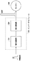
図1は、実施の形態に係る回路装置が用いられるインバータモジュールを示す概略図である。図2は、インバータモジュールの構成を示す概略図である。インバータモジュール500には、PWM(Pulse Width Moduration)信号が入力される。インバータモジュール500に入力されるPWM信号は、通常、ロジックレベル(5V)である。PWM信号を受信したインバータモジュール500は、U相、V相、W相の3つの相(コイル)を有するモータ530の各相に位相の異なる交流電流(500V振幅)を供給することにより、モータ530を回転させる。インバータモジュール500は、電圧増幅部510および電力増幅部520を備える。電圧増幅部510は、U相、V相、W相にそれぞれ対応する昇圧回路512、514、516を有する。昇圧回路512、514、516において、それぞれ入力されたPWM信号が15Vに昇圧される。電力増幅部520は、U相に対応するパワー素子521、524、V相に対応するパワー素子522、525およびW相に対応するパワー素子523、526を有する。U相、V相、W相にそれぞれ対応する一組のパワー素子のオンオフにより、PWM信号の電力が増幅される。
(Embodiment)
FIG. 1 is a schematic diagram illustrating an inverter module in which the circuit device according to the embodiment is used. FIG. 2 is a schematic diagram showing the configuration of the inverter module. The
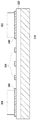
図3は、実施の形態に係る回路装置の断面図である。図3の断面は、たとえば、図2のA−A’線上の断面に相当する。本実施の形態の回路装置10は、金属基板20、絶縁層30、第1の配線40、第2の配線50a,50b、および回路素子60を備える。
FIG. 3 is a cross-sectional view of the circuit device according to the embodiment. The cross section in FIG. 3 corresponds to the cross section on the line A-A ′ in FIG. 2, for example. The
金属基板20には、凹部22が設けられている。凹部22の深さは、たとえば、約60μm〜約1mm、典型的には約200μmである。金属基板20の上面のうち、凹部22を除いた領域を凸部24とよぶ。凸部24における金属基板20の厚さは、たとえば、約100μm〜約3mm、典型的には約1.5mmである。金属基板20を構成する材料としては、たとえば、アルミニウム、銅などが挙げられる。また、金属基板20は、銅からなる下層金属層と、下層金属層上に形成されたFe−Ni系合金(いわゆるインバー合金)からなる中間金属層と、中間金属層上に形成された銅からなる上層金属層とが積層されたクラッド材であってもよい。
The
絶縁層30は、金属基板20の上に形成されている。すなわち、凹部22には、絶縁層30が充填されている。絶縁層30の厚さは、たとえば、約60μm〜約160μmである。絶縁層30を構成する材料としては、たとえば、BTレジン等のメラミン誘導体、液晶ポリマー、エポキシ樹脂、PPE樹脂、ポリイミド樹脂、フッ素樹脂、フェノール樹脂、ポリアミドビスマレイミド等の熱硬化性樹脂が例示される。回路装置10の放熱性向上の観点から、絶縁層30は高熱伝導性を有することが望ましい。このため、絶縁層30は、アルミニウム化合物、カルシウム化合物、カリウム化合物、マグネシウム化合物またはケイ素化合物などを高伝導性フィラーとして含有することが好ましい。
The
第1の配線40は、金属基板20に形成された凹部22の上方の絶縁層30に埋め込まれている。第1の配線40は、たとえば、銅などの導電部材により形成される。第1の配線40には、高電圧の信号が伝送される。ここで、高電圧とは、後述する回路素子60(パワー素子)の駆動電圧(たとえば15V)より高い電圧をいう。典型的には、ハイブリッド自動車のモータ用インバータモジュールの場合、高電圧とは、500〜600Vである。
The
本実施の形態のように、第1の配線40が複数設けられている場合には、絶縁層30によって隣接する第1の配線40の間が絶縁されている。これにより、隣接する第1の配線40が空気により絶縁されている場合に比べて、第1の配線40の間隔Hを短くすることができる。第1の配線40の間隔Hを短くすることにより、回路装置10のさらなる小型化を図ることができる。
When a plurality of
具体的には、空気の絶縁耐圧をW(V/m)とし、第1の配線40によって伝送される信号の電圧をP(V)とし、隣接する第1の配線40の間隔をHとしたときに、
H<P/W
の関係が成り立つ。すなわち、空気の絶縁耐圧で決まる最小の配線間隔H0=P/Wよりも配線間隔を短くすることができる。
Specifically, the withstand voltage of air is W (V / m), the voltage of the signal transmitted by the
H <P / W
The relationship holds. That is, the wiring interval can be made shorter than the minimum wiring interval H 0 = P / W determined by the dielectric strength voltage of air.
第2の配線50a,50bは、金属基板20の凸部24の上方の絶縁層30の上に形成されている。第2の配線50a,50bは、たとえば、銅などの導電部材により形成される。第2の配線50aは所定の配線パターンを有し、ロジックレベル(たとえば5V)の低電圧の信号が伝送される。一方、第2の配線50bは高電圧が印加される。
The
回路素子60は、IC、LSIなどの半導体素子であり、図2に関連して説明したパワー素子に相当する。回路素子60は、はんだなどの接着部材を介して第2の配線50bの上に搭載されている。典型的には、回路素子60をMOSFETとした場合に、回路素子60のドレインに第2の配線50bが接続される。なお、回路素子60の放熱性を向上させるために、回路素子60と第2の配線50bとの間に、銅などの金属からなる放熱プレートを設けてもよい。
The
(製造方法)
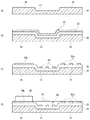
図4(A)〜(D)は、図3に示した実施の形態に係る回路装置の製造プロセスを説明するための工程断面図である。まず、図4(A)に示すように、凹部22が形成された金属基板20を用意する。金属基板20の材料として、たとえば、アルミニウムを用いる。金属基板20に凹部22を形成する方法は限定されないが、たとえば、薬液処理が挙げられる。ここで、凸部24における金属基板20の厚さは、約100μm〜約3mm、典型的には約1.5mmである。また、凹部22の深さは、約60μm〜約1mm、典型的には約200μmである。
(Production method)
4A to 4D are process cross-sectional views for explaining a manufacturing process of the circuit device according to the embodiment shown in FIG. First, as shown in FIG. 4A, a
次に、図4(B)に示すように、金属基板20の上面に、アルミナまたはシリカなどの充填材が添加されたエポキシ樹脂を塗布することによって、約60μm〜約160μmの厚みを有する第1の絶縁層32を形成する。続いて、第1の絶縁層32の上に約70μmの厚みを有する銅箔52を圧着する。このとき、第1の絶縁層32および銅箔52は凹部22に沿って形成されるため、凹部22の上方において窪んだ形状が形成される。
Next, as shown in FIG. 4B, by applying an epoxy resin to which a filler such as alumina or silica is added to the upper surface of the
次に、図4(C)に示すように、フォトリソグラフィ技術およびエッチング技術を用いて、銅箔52をパターニングすることにより、第1の配線40および第2の配線50a,50bを形成する。ここで、第2の配線50aは、低電圧が印加されるパターニングされた配線である。一方、第2の配線50bは、高電圧が印加される配線である。このとき、第1の配線40は凹部22の上方の窪んだ部分において形成されるため、第2の配線50a,50bに比べて凹部22の深さの分だけ下方に位置する。
Next, as shown in FIG. 4C, the
次に、図4(D)に示すように、凹部22の上方に形成された第1の配線40のみを覆う(凹部22以外に形成された第2の配線50a,50bの表面は露出する)ように第2の絶縁層34を形成する。第2の絶縁層34は、たとえば、アルミナまたはシリカなどの充填剤が添加されたエポキシ樹脂をスキージングなどの手法により塗布することによって形成することができる。なお、第1の絶縁層32および第2の絶縁層34を合わせた層が、図3に示した絶縁層30に相当する。この後、表面が露出した第2の配線50bにはんだなどの融着層を介して回路素子60を装着する。回路素子60は、上述したように、LSIなどのパワー素子である。たとえば、回路素子60をMOSFETとした場合に、第2の配線50bは回路素子60のドレインに接続される。
Next, as shown in FIG. 4D, only the
以上の製造プロセスにより図3に示した実施の形態に係る回路装置を製造することができる。 The circuit device according to the embodiment shown in FIG. 3 can be manufactured by the above manufacturing process.
以上説明した回路装置によれば、高圧配線間のスペースが絶縁層の絶縁耐圧に応じて設定することができる。空気に比べて高耐圧の絶縁層を使用することにより、高圧配線間のスペース圧縮が可能となり、基板面積削減に寄与する。 According to the circuit device described above, the space between the high-voltage wirings can be set according to the withstand voltage of the insulating layer. By using an insulating layer having a higher withstand voltage than air, the space between the high-voltage wirings can be compressed, which contributes to a reduction in the board area.
また、発熱素子であるパワー素子を金属基板の凸部上方に配置することにより、発熱部品と金属基板との距離を小さくすることができ、金属基板を介して放熱をより効果的に行うことができる。特に、高電力効率特性と高放熱特性との両立とモジュールの小型化が厳しく要求される車載用インバータモジュールは、上述したの回路装置を用いることが効果的である。 Moreover, by disposing the power element, which is a heat generating element, above the convex portion of the metal substrate, the distance between the heat generating component and the metal substrate can be reduced, and heat can be radiated more effectively through the metal substrate. it can. In particular, in-vehicle inverter modules for which both high power efficiency characteristics and high heat dissipation characteristics are required and miniaturization of modules is strictly required, it is effective to use the above-described circuit device.
本発明は、上述の各実施の形態に限定されるものではなく、当業者の知識に基づいて各種の設計変更等の変形を加えることも可能であり、そのような変形が加えられた実施の形態も本発明の範囲に含まれうるものである。 The present invention is not limited to the above-described embodiments, and various modifications such as design changes can be added based on the knowledge of those skilled in the art. The form can also be included in the scope of the present invention.
例えば、上述の実施の形態では、回路素子60が第2の配線50bの上に搭載されているが、回路素子60は、絶縁層30の上に搭載されていてもよい。
For example, in the above-described embodiment, the
10 回路装置、20 金属基板、30 絶縁層、40 第1の配線、50a,50b 第2の配線、60 回路素子。
DESCRIPTION OF
Claims (4)
前記金属基板の上に設けられた絶縁層と、
前記凹部の上方に位置する前記絶縁層に埋め込まれ、高電圧の信号が伝送される複数のの第1の配線と、
前記凹部以外において前記絶縁層を介して前記金属基板の上方に位置する第2の配線と、
前記絶縁層の上方に設けられた回路素子と、
を備え、
前記複数の第1の配線と前記金属基板との距離と、前記第2の配線と前記金属基板との距離が同等であることを特徴とする回路装置。 A metal substrate with a recess,
An insulating layer provided on the metal substrate;
A plurality of first wirings embedded in the insulating layer located above the recesses and transmitting a high-voltage signal;
A second wiring located above the metal substrate through the insulating layer except for the recess;
A circuit element provided above the insulating layer;
Equipped with a,
The circuit device characterized in that a distance between the plurality of first wirings and the metal substrate is equal to a distance between the second wiring and the metal substrate .
H<P/W
なる関係が成立していることを特徴とする請求項1に記載の回路装置。 When the interval between the plurality of first wires is H (mm), the dielectric strength of air is W (V / mm), and the voltage of the wires is P (V),
H <P / W
The circuit device according to claim 1, wherein the following relationship is established.
Priority Applications (1)
| Application Number | Priority Date | Filing Date | Title |
|---|---|---|---|
| JP2007170561A JP5002350B2 (en) | 2007-06-28 | 2007-06-28 | Circuit equipment |
Applications Claiming Priority (1)
| Application Number | Priority Date | Filing Date | Title |
|---|---|---|---|
| JP2007170561A JP5002350B2 (en) | 2007-06-28 | 2007-06-28 | Circuit equipment |
Publications (3)
| Publication Number | Publication Date |
|---|---|
| JP2009010192A JP2009010192A (en) | 2009-01-15 |
| JP2009010192A5 JP2009010192A5 (en) | 2010-08-26 |
| JP5002350B2 true JP5002350B2 (en) | 2012-08-15 |
Family
ID=40324983
Family Applications (1)
| Application Number | Title | Priority Date | Filing Date |
|---|---|---|---|
| JP2007170561A Expired - Fee Related JP5002350B2 (en) | 2007-06-28 | 2007-06-28 | Circuit equipment |
Country Status (1)
| Country | Link |
|---|---|
| JP (1) | JP5002350B2 (en) |
Families Citing this family (2)
| Publication number | Priority date | Publication date | Assignee | Title |
|---|---|---|---|---|
| WO2013046617A1 (en) * | 2011-09-28 | 2013-04-04 | 三洋電機株式会社 | Substrate for mounting element thereon, semiconductor module, and method for manufacturing substrate for mounting element thereon |
| KR101204564B1 (en) * | 2011-09-30 | 2012-11-23 | 삼성전기주식회사 | Power Module Package And Method of Manufacturing The Same |
Family Cites Families (4)
| Publication number | Priority date | Publication date | Assignee | Title |
|---|---|---|---|---|
| JPH08316592A (en) * | 1995-05-23 | 1996-11-29 | Fujitsu Ltd | Circuit board and production thereof |
| JP2002280686A (en) * | 2001-03-15 | 2002-09-27 | Nippon Avionics Co Ltd | Metal core printed wiring board and its manufacturing method |
| TWI267173B (en) * | 2004-03-29 | 2006-11-21 | Sanyo Electric Co | Circuit device and method for manufacturing thereof |
| JP2006100753A (en) * | 2004-09-30 | 2006-04-13 | Sanyo Electric Co Ltd | Semiconductor module and its manufacturing method |
-
2007
- 2007-06-28 JP JP2007170561A patent/JP5002350B2/en not_active Expired - Fee Related
Also Published As
| Publication number | Publication date |
|---|---|
| JP2009010192A (en) | 2009-01-15 |
Similar Documents
| Publication | Publication Date | Title |
|---|---|---|
| KR100661948B1 (en) | Circuit device and manufacturing method thereof | |
| JP2009010309A (en) | Semiconductor device and its manufacturing method, and display and its manufacturing method | |
| US6803257B2 (en) | Printed circuit board with a heat dissipation element, method for manufacturing the printed circuit board, and package comprising the printed circuit board | |
| KR100661946B1 (en) | Circuit device and manufacturing method thereof | |
| US10154593B2 (en) | Electronic assembly group and method for producing the same | |
| JP6033215B2 (en) | Power module semiconductor device | |
| JP2007103939A (en) | Printed circuit board incorporating electronic element and manufacturing method of the same | |
| JP2008205142A (en) | Wiring board for cof, manufacturing method thereof and semiconductor device | |
| JP2008042074A (en) | Semiconductor device and power conversion device | |
| JP2010080572A (en) | Electronic equipment | |
| US20170309556A1 (en) | Electronic part mounting heat-dissipating substrate | |
| JP4882562B2 (en) | Thermally conductive substrate, manufacturing method thereof, power supply unit, and electronic device | |
| JP2009076897A (en) | Device having connection device and at least one semiconductor element | |
| US20070252270A1 (en) | Circuit Apparatus | |
| JP4344766B2 (en) | Source driver, source driver manufacturing method, and liquid crystal module | |
| JP2008124247A (en) | Substrate with built-in component and its manufacturing method | |
| JP5169800B2 (en) | Electronic equipment | |
| JP5002350B2 (en) | Circuit equipment | |
| JP2008288273A (en) | Wiring substrate for cof (chip on film), manufacturing metod of the same, and semiconductor device | |
| JP2006100759A (en) | Circuit device and its manufacturing method | |
| JP4975584B2 (en) | Semiconductor device and manufacturing method of semiconductor device. | |
| JP2008205141A (en) | Wiring board for cof, manufacturing method thereof and cof | |
| US20120080770A1 (en) | Transformer Arrangement | |
| JP2008021817A (en) | Heat conducting base board, manufacturing method thereof, power supply unit, and electronic equipment | |
| JP2010040569A (en) | Electronic component module |
Legal Events
| Date | Code | Title | Description |
|---|---|---|---|
| A521 | Written amendment |
Free format text: JAPANESE INTERMEDIATE CODE: A523 Effective date: 20100617 |
|
| A621 | Written request for application examination |
Free format text: JAPANESE INTERMEDIATE CODE: A621 Effective date: 20100617 |
|
| A521 | Written amendment |
Free format text: JAPANESE INTERMEDIATE CODE: A523 Effective date: 20100712 |
|
| A977 | Report on retrieval |
Free format text: JAPANESE INTERMEDIATE CODE: A971007 Effective date: 20110405 |
|
| A131 | Notification of reasons for refusal |
Free format text: JAPANESE INTERMEDIATE CODE: A131 Effective date: 20111025 |
|
| A521 | Written amendment |
Free format text: JAPANESE INTERMEDIATE CODE: A523 Effective date: 20111222 |
|
| TRDD | Decision of grant or rejection written | ||
| A01 | Written decision to grant a patent or to grant a registration (utility model) |
Free format text: JAPANESE INTERMEDIATE CODE: A01 Effective date: 20120424 |
|
| A01 | Written decision to grant a patent or to grant a registration (utility model) |
Free format text: JAPANESE INTERMEDIATE CODE: A01 |
|
| A61 | First payment of annual fees (during grant procedure) |
Free format text: JAPANESE INTERMEDIATE CODE: A61 Effective date: 20120521 |
|
| FPAY | Renewal fee payment (prs date is renewal date of database) |
Free format text: PAYMENT UNTIL: 20150525 Year of fee payment: 3 |
|
| LAPS | Cancellation because of no payment of annual fees |