JP4993754B2 - PGA type wiring board and manufacturing method thereof - Google Patents
PGA type wiring board and manufacturing method thereof Download PDFInfo
- Publication number
- JP4993754B2 JP4993754B2 JP2008041441A JP2008041441A JP4993754B2 JP 4993754 B2 JP4993754 B2 JP 4993754B2 JP 2008041441 A JP2008041441 A JP 2008041441A JP 2008041441 A JP2008041441 A JP 2008041441A JP 4993754 B2 JP4993754 B2 JP 4993754B2
- Authority
- JP
- Japan
- Prior art keywords
- wiring board
- pin
- fixing plate
- hole
- pin fixing
- Prior art date
- Legal status (The legal status is an assumption and is not a legal conclusion. Google has not performed a legal analysis and makes no representation as to the accuracy of the status listed.)
- Active
Links
Images


Classifications
-
- H—ELECTRICITY
- H05—ELECTRIC TECHNIQUES NOT OTHERWISE PROVIDED FOR
- H05K—PRINTED CIRCUITS; CASINGS OR CONSTRUCTIONAL DETAILS OF ELECTRIC APPARATUS; MANUFACTURE OF ASSEMBLAGES OF ELECTRICAL COMPONENTS
- H05K1/00—Printed circuits
- H05K1/02—Details
- H05K1/11—Printed elements for providing electric connections to or between printed circuits
-
- H—ELECTRICITY
- H05—ELECTRIC TECHNIQUES NOT OTHERWISE PROVIDED FOR
- H05K—PRINTED CIRCUITS; CASINGS OR CONSTRUCTIONAL DETAILS OF ELECTRIC APPARATUS; MANUFACTURE OF ASSEMBLAGES OF ELECTRICAL COMPONENTS
- H05K3/00—Apparatus or processes for manufacturing printed circuits
- H05K3/30—Assembling printed circuits with electric components, e.g. with resistor
- H05K3/303—Surface mounted components, e.g. affixing before soldering, aligning means, spacing means
-
- H—ELECTRICITY
- H01—ELECTRIC ELEMENTS
- H01L—SEMICONDUCTOR DEVICES NOT COVERED BY CLASS H10
- H01L21/00—Processes or apparatus adapted for the manufacture or treatment of semiconductor or solid state devices or of parts thereof
- H01L21/02—Manufacture or treatment of semiconductor devices or of parts thereof
- H01L21/04—Manufacture or treatment of semiconductor devices or of parts thereof the devices having at least one potential-jump barrier or surface barrier, e.g. PN junction, depletion layer or carrier concentration layer
- H01L21/50—Assembly of semiconductor devices using processes or apparatus not provided for in a single one of the subgroups H01L21/06 - H01L21/326, e.g. sealing of a cap to a base of a container
- H01L21/60—Attaching or detaching leads or other conductive members, to be used for carrying current to or from the device in operation
-
- H—ELECTRICITY
- H01—ELECTRIC ELEMENTS
- H01L—SEMICONDUCTOR DEVICES NOT COVERED BY CLASS H10
- H01L23/00—Details of semiconductor or other solid state devices
- H01L23/48—Arrangements for conducting electric current to or from the solid state body in operation, e.g. leads, terminal arrangements ; Selection of materials therefor
-
- H—ELECTRICITY
- H01—ELECTRIC ELEMENTS
- H01L—SEMICONDUCTOR DEVICES NOT COVERED BY CLASS H10
- H01L2224/00—Indexing scheme for arrangements for connecting or disconnecting semiconductor or solid-state bodies and methods related thereto as covered by H01L24/00
- H01L2224/01—Means for bonding being attached to, or being formed on, the surface to be connected, e.g. chip-to-package, die-attach, "first-level" interconnects; Manufacturing methods related thereto
- H01L2224/10—Bump connectors; Manufacturing methods related thereto
- H01L2224/15—Structure, shape, material or disposition of the bump connectors after the connecting process
- H01L2224/16—Structure, shape, material or disposition of the bump connectors after the connecting process of an individual bump connector
- H01L2224/161—Disposition
- H01L2224/16151—Disposition the bump connector connecting between a semiconductor or solid-state body and an item not being a semiconductor or solid-state body, e.g. chip-to-substrate, chip-to-passive
- H01L2224/16221—Disposition the bump connector connecting between a semiconductor or solid-state body and an item not being a semiconductor or solid-state body, e.g. chip-to-substrate, chip-to-passive the body and the item being stacked
- H01L2224/16225—Disposition the bump connector connecting between a semiconductor or solid-state body and an item not being a semiconductor or solid-state body, e.g. chip-to-substrate, chip-to-passive the body and the item being stacked the item being non-metallic, e.g. insulating substrate with or without metallisation
-
- H—ELECTRICITY
- H05—ELECTRIC TECHNIQUES NOT OTHERWISE PROVIDED FOR
- H05K—PRINTED CIRCUITS; CASINGS OR CONSTRUCTIONAL DETAILS OF ELECTRIC APPARATUS; MANUFACTURE OF ASSEMBLAGES OF ELECTRICAL COMPONENTS
- H05K2201/00—Indexing scheme relating to printed circuits covered by H05K1/00
- H05K2201/10—Details of components or other objects attached to or integrated in a printed circuit board
- H05K2201/10227—Other objects, e.g. metallic pieces
- H05K2201/1031—Surface mounted metallic connector elements
- H05K2201/10318—Surface mounted metallic pins
-
- H—ELECTRICITY
- H05—ELECTRIC TECHNIQUES NOT OTHERWISE PROVIDED FOR
- H05K—PRINTED CIRCUITS; CASINGS OR CONSTRUCTIONAL DETAILS OF ELECTRIC APPARATUS; MANUFACTURE OF ASSEMBLAGES OF ELECTRICAL COMPONENTS
- H05K2201/00—Indexing scheme relating to printed circuits covered by H05K1/00
- H05K2201/10—Details of components or other objects attached to or integrated in a printed circuit board
- H05K2201/10227—Other objects, e.g. metallic pieces
- H05K2201/10424—Frame holders
-
- H—ELECTRICITY
- H05—ELECTRIC TECHNIQUES NOT OTHERWISE PROVIDED FOR
- H05K—PRINTED CIRCUITS; CASINGS OR CONSTRUCTIONAL DETAILS OF ELECTRIC APPARATUS; MANUFACTURE OF ASSEMBLAGES OF ELECTRICAL COMPONENTS
- H05K2201/00—Indexing scheme relating to printed circuits covered by H05K1/00
- H05K2201/10—Details of components or other objects attached to or integrated in a printed circuit board
- H05K2201/10613—Details of electrical connections of non-printed components, e.g. special leads
- H05K2201/10954—Other details of electrical connections
- H05K2201/10977—Encapsulated connections
-
- H—ELECTRICITY
- H05—ELECTRIC TECHNIQUES NOT OTHERWISE PROVIDED FOR
- H05K—PRINTED CIRCUITS; CASINGS OR CONSTRUCTIONAL DETAILS OF ELECTRIC APPARATUS; MANUFACTURE OF ASSEMBLAGES OF ELECTRICAL COMPONENTS
- H05K3/00—Apparatus or processes for manufacturing printed circuits
- H05K3/22—Secondary treatment of printed circuits
- H05K3/28—Applying non-metallic protective coatings
- H05K3/284—Applying non-metallic protective coatings for encapsulating mounted components
-
- H—ELECTRICITY
- H05—ELECTRIC TECHNIQUES NOT OTHERWISE PROVIDED FOR
- H05K—PRINTED CIRCUITS; CASINGS OR CONSTRUCTIONAL DETAILS OF ELECTRIC APPARATUS; MANUFACTURE OF ASSEMBLAGES OF ELECTRICAL COMPONENTS
- H05K3/00—Apparatus or processes for manufacturing printed circuits
- H05K3/30—Assembling printed circuits with electric components, e.g. with resistor
- H05K3/303—Surface mounted components, e.g. affixing before soldering, aligning means, spacing means
- H05K3/305—Affixing by adhesive
-
- H—ELECTRICITY
- H05—ELECTRIC TECHNIQUES NOT OTHERWISE PROVIDED FOR
- H05K—PRINTED CIRCUITS; CASINGS OR CONSTRUCTIONAL DETAILS OF ELECTRIC APPARATUS; MANUFACTURE OF ASSEMBLAGES OF ELECTRICAL COMPONENTS
- H05K3/00—Apparatus or processes for manufacturing printed circuits
- H05K3/30—Assembling printed circuits with electric components, e.g. with resistor
- H05K3/32—Assembling printed circuits with electric components, e.g. with resistor electrically connecting electric components or wires to printed circuits
- H05K3/34—Assembling printed circuits with electric components, e.g. with resistor electrically connecting electric components or wires to printed circuits by soldering
- H05K3/341—Surface mounted components
- H05K3/3421—Leaded components
- H05K3/3426—Leaded components characterised by the leads
-
- Y—GENERAL TAGGING OF NEW TECHNOLOGICAL DEVELOPMENTS; GENERAL TAGGING OF CROSS-SECTIONAL TECHNOLOGIES SPANNING OVER SEVERAL SECTIONS OF THE IPC; TECHNICAL SUBJECTS COVERED BY FORMER USPC CROSS-REFERENCE ART COLLECTIONS [XRACs] AND DIGESTS
- Y02—TECHNOLOGIES OR APPLICATIONS FOR MITIGATION OR ADAPTATION AGAINST CLIMATE CHANGE
- Y02P—CLIMATE CHANGE MITIGATION TECHNOLOGIES IN THE PRODUCTION OR PROCESSING OF GOODS
- Y02P70/00—Climate change mitigation technologies in the production process for final industrial or consumer products
- Y02P70/50—Manufacturing or production processes characterised by the final manufactured product
-
- Y—GENERAL TAGGING OF NEW TECHNOLOGICAL DEVELOPMENTS; GENERAL TAGGING OF CROSS-SECTIONAL TECHNOLOGIES SPANNING OVER SEVERAL SECTIONS OF THE IPC; TECHNICAL SUBJECTS COVERED BY FORMER USPC CROSS-REFERENCE ART COLLECTIONS [XRACs] AND DIGESTS
- Y10—TECHNICAL SUBJECTS COVERED BY FORMER USPC
- Y10T—TECHNICAL SUBJECTS COVERED BY FORMER US CLASSIFICATION
- Y10T29/00—Metal working
- Y10T29/49—Method of mechanical manufacture
- Y10T29/49002—Electrical device making
- Y10T29/49117—Conductor or circuit manufacturing
- Y10T29/49124—On flat or curved insulated base, e.g., printed circuit, etc.
- Y10T29/49128—Assembling formed circuit to base
Description
本発明は、半導体素子等の電子部品を実装するのに用いられる配線基板に関し、特に、電子部品実装面側と反対側の面に外部接続端子として用いられる多数のピンが立設されたピン・グリッド・アレイ(PGA)型配線基板(以下、便宜上、「半導体パッケージ」もしくは単に「パッケージ」ともいう。)及びその製造方法に関する。 The present invention relates to a wiring board used for mounting an electronic component such as a semiconductor element, and in particular, a pin in which a large number of pins used as external connection terminals are erected on the surface opposite to the electronic component mounting surface side. The present invention relates to a grid array (PGA) type wiring board (hereinafter also referred to as “semiconductor package” or simply “package”) and a method for manufacturing the same.
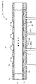
図10(a)は、従来のPGA型配線基板の一例を示したものである。このPGA型配線基板60において、61は配線基板本体を構成する樹脂基板、62及び63はそれぞれ樹脂基板61の両面に所要の形状にパターニング形成された配線層、64及び65はそれぞれ各配線層62,63の所要の箇所に画定されたパッド部を除いて両面を覆うように形成された保護膜(絶縁層)を示す。また、樹脂基板61のチップ実装面側のパッド部(配線層62)には、IC等のチップ(電子部品)を実装する際にその電極端子と接続するためのはんだ66が被着されており、これと反対側のパッド部(配線層63)には、はんだ67を介して、本配線基板60をマザーボード等の実装用基板に実装する際に使用される外部接続端子としてのピン68が接合されている。
FIG. 10A shows an example of a conventional PGA type wiring board. In this PGA
現状の技術では、IC(チップ)側の接続に使用するはんだ66として、錫(Sn)−鉛(Pb)系の共晶はんだ(組成がSn:62%、Pb:38%、融点が183℃前後)が主に使用されている。一方、ピン68の接続には、同じSn−Pb系のはんだの一種である、鉛(Pb)を多く含む高温はんだ(例えば、Sn、Pb、アンチモン(Sb)からなる融点が240℃前後のはんだ)が使用されている。
In the current technology, tin (Sn) -lead (Pb) eutectic solder (composition is Sn: 62%, Pb: 38%, melting point is 183 ° C.) as the
このようにIC接続用のはんだには比較的低融点のものを使用する一方で、ピン接続用のはんだには比較的高融点のものを使用する理由は、パッケージ基板にピンを接合(ピンニング)した後の段階で行うIC(チップ)の実装時のリフローの際にピン接続用のはんだが溶融しないようにするためである。 The reason for using a relatively high melting point as the solder for connecting pins while using a solder with a relatively high melting point as the solder for connecting pins is as follows. This is to prevent the solder for pin connection from melting at the time of reflow when mounting the IC (chip) performed at a later stage.
その一方で、最近の鉛フリー化のトレンドにより、比較的高温の融点を有したはんだの使用への切替が進んでおり、IC側の接続についても、従来の比較的低融点のはんだ(融点が183℃前後のSn/Pb系の共晶はんだ)に代えて、比較的高融点のはんだ(例えば、Snと銀(Ag)と銅(Cu)の組成からなり、融点が220℃前後の鉛フリーはんだ)の使用が要求されるようになってきている。これに伴い、ICの実装時のリフロー温度(IC接続用のはんだの融点)がピン側のはんだの融点に迫るようになってきた。 On the other hand, due to the recent trend of lead-free, the use of solder having a relatively high melting point is proceeding, and the conventional relatively low melting point solder (with a melting point of Instead of Sn / Pb eutectic solder at around 183 ° C., it has a relatively high melting point solder (for example, Sn, silver (Ag) and copper (Cu)), and the lead-free melting point is around 220 ° C. The use of solder) has been required. Accordingly, the reflow temperature at the time of mounting the IC (melting point of the solder for connecting the IC) approaches the melting point of the solder on the pin side.
かかる従来技術に関連する技術としては、例えば、特許文献1に記載されたPGA型電子部品用基板がある。また、特許文献2に記載されたピン付きプリント配線板およびその製造方法がある。
上述したように従来の技術では、ピン接続用のはんだには、IC接続用のはんだよりも高温の融点を有したはんだを使用することで、ICアセンブリでのリフローの際にピン接続用のはんだが溶融しないようにしていた。その一方で、鉛フリー化の影響により、IC側の接続についても、低融点の共晶はんだの使用から高融点の鉛フリーはんだの使用への切替が進み、IC接続用のはんだの融点がピン接続用のはんだの融点に近づいている。このため、以下のような問題が生じていた。 As described above, in the prior art, the solder for pin connection uses a solder having a higher melting point than the solder for IC connection, so that the solder for pin connection during reflow in the IC assembly is used. Was not melted. On the other hand, due to the effects of lead-free soldering, the use of eutectic solder with a low melting point has been switched to the use of lead-free solder with a high melting point for the connection on the IC side. The melting point of the connecting solder is approaching. For this reason, the following problems have arisen.
先ず、ピンニング後(ピンの接合後)のICアセンブリ時に、IC接続用として設けた高融点のはんだをリフローにより溶融させてチップの電極端子との接続を行うが、その際のリフロー温度がピン側のはんだの融点に近いため、その影響を受けてピン側のはんだも溶融するといった不都合が起こり得る。ピン側のはんだが溶融すると、ピンニング工程において正規の状態で立設されたピンの姿勢が安定せず、場合によってはピンが傾いてしまうといった問題があった。 First, at the time of IC assembly after pinning (after pin joining), a high melting point solder provided for IC connection is melted by reflow to connect to the electrode terminal of the chip, and the reflow temperature at that time is the pin side Since this is close to the melting point of the solder, there is a possibility that the solder on the pin side also melts due to the influence. When the solder on the pin side melts, there is a problem that the posture of the pin erected in a normal state in the pinning process is not stable, and the pin is inclined in some cases.
図10(b)はその一例を模式的に示したものであり、配線基板60に設けた4本のピン68のうち最も左側のピンの軸部68bが右方向に傾いている状態を示している。このようにピンが傾いてしまうと、その先端部の位置は本来の設計位置から変位するため、このピンを受け入れる側のソケットに挿入させることができない(つまり、ピンとソケットとの接続信頼性が損なわれる)といった不都合が生じる。
FIG. 10B schematically shows an example thereof, and shows a state in which the
また、IC接続時のリフロー温度の影響を受けてピン側のはんだが溶融すると、その溶融したはんだが、ピンのヘッド部から先端部に向かって這い上がってしまう(つまり、ピンの軸部に不要なはんだが付着する)といった現象が発生する。このとき、その這い上がる高さ(はんだが付着する部分)がピンのヘッド部近傍に留まっていれば特に問題はないが、ピンを当該パッド部に接合するのに使用したはんだの量や加熱温度などの条件によっては、はんだがピンの先端部近傍まで這い上がってしまう場合も起こり得る。 Also, if the solder on the pin side melts due to the influence of the reflow temperature at the time of IC connection, the melted solder crawls up from the head part of the pin toward the tip part (that is, it is not necessary for the shaft part of the pin) A phenomenon that a small solder adheres) occurs. At this time, there is no particular problem if the creeping height (the part where the solder adheres) stays in the vicinity of the head of the pin, but the amount of solder used to join the pin to the pad and the heating temperature Depending on the conditions, the solder may crawl up to the vicinity of the tip of the pin.
例えば、図10(b)において、左から2番目のピン68については、その軸部68bにはんだ67aが付着している部分はピンのヘッド部68aの近傍に留まっているが、最も右側のピン68については、その軸部68bにはんだ67bが付着している部分は先端部の近傍に及んでいる。このようにはんだがピンの先端部近傍まで付着していると、その部分のピンの直径(太さ)が大きくなるため、このピンを受け入れる側のソケットにうまく入らないといった問題があった。
For example, in FIG. 10B, for the
本発明は、かかる従来技術における課題に鑑み創作されたもので、ピンニング後の電子部品の実装の際の熱処理温度がピン側の導電性材料の融点を超えた場合でも、ピンが傾くことなくその立設状態を安定に保ち、その導電性材料が外部に漏れ出すのを確実に防止することができるPGA型配線基板及びその製造方法を提供することを目的とする。 The present invention was created in view of such problems in the prior art, and even when the heat treatment temperature when mounting electronic components after pinning exceeds the melting point of the conductive material on the pin side, the pin does not tilt. It is an object of the present invention to provide a PGA type wiring board capable of maintaining a standing state stably and reliably preventing the conductive material from leaking to the outside and a manufacturing method thereof.
上記した従来技術の課題を解決するため、本発明の一形態によれば、表面にパッド部が形成された配線基板と、ヘッド部及び該ヘッド部に接合された軸部を有するピンと、貫通孔が形成されたピン固定用板とを備え、前記ピンのヘッド部が、導電性材料を介して前記パッド部に接合され、前記ピン固定用板が、接着剤層を介して前記配線基板の表面に接着され、前記貫通孔に前記ピンの軸部が挿通されると共に、前記接着剤層の接着剤が、前記貫通孔と前記軸部との隙間に充填され、且つ前記軸部上を前記貫通孔の外まで這い上がっていることを特徴とするPGA型配線基板が提供される。 In order to solve the above-described problems of the prior art, according to one aspect of the present invention, a wiring board having a pad portion formed on the surface, a pin having a head portion and a shaft portion joined to the head portion, and a through hole The pin fixing plate is bonded to the pad portion via a conductive material, and the pin fixing plate is connected to the surface of the wiring board via an adhesive layer. The shaft portion of the pin is inserted into the through hole, and the adhesive of the adhesive layer is filled in the gap between the through hole and the shaft portion, and the penetrating portion is passed through the shaft portion. There is provided a PGA type wiring board characterized by crawling up to the outside of the hole .
この形態に係るPGA型配線基板の構成によれば、配線基板のパッド部に接合されたピンのヘッド部がその周囲を接着剤層によって覆われ、さらに、貫通孔とピンの軸部との隙間に接着剤が充填されると共に、貫通孔内から軸部上に這い上がっている。つまり、接着剤層を介在させてピン固定用板によりヘッド部及びその近傍部分が固定化されている。この構造により、ピンニング後の電子部品(IC等のチップなど)の実装時にその熱処理温度(リフロー温度)がピン側の導電性材料(はんだ)の融点を超えた場合でも、従来技術(図10(b))に見られたようなピンが傾くといった不都合を解消することができる。つまり、ピンニング工程において正規の状態で立設したピンの姿勢を電子部品実装中もそのまま安定に保つことができる。 According to the configuration of the PGA type wiring board according to this embodiment , the head part of the pin joined to the pad part of the wiring board is covered with the adhesive layer, and further , the gap between the through hole and the shaft part of the pin Is filled with an adhesive, and crawls up from the through hole onto the shaft. That is, the head portion and its vicinity are fixed by the pin fixing plate with the adhesive layer interposed . With this structure, even when an electronic component (such as a chip such as an IC) after pinning is mounted, even when the heat treatment temperature (reflow temperature) exceeds the melting point of the conductive material (solder) on the pin side, the conventional technology (FIG. The inconvenience that the pin is inclined as seen in b)) can be solved. That is, the posture of the pins erected in the normal state in the pinning process can be kept stable even during the mounting of the electronic component.
また、ピン固定用板の貫通孔とこれを挿通したピンとの隙間にも接着剤層の一部が充填されるので、この接着剤層の介在により、熱処理の際にピン側の導電性材料(はんだ)が外部に漏れ出すのを確実に防止することができる。つまり、従来技術(図10(b))に見られたような不都合(溶融したピン側のはんだがヘッド部から先端部に向かって這い上がってしまい、ピンの軸部に不要なはんだが付着すること)を解消することができる。 In addition, since a part of the adhesive layer is also filled in the gap between the through hole of the pin fixing plate and the pin inserted therethrough, the conductive material on the pin side ( It is possible to reliably prevent the solder) from leaking to the outside. That is, inconveniences as seen in the prior art (FIG. 10 (b)) (the molten pin side solder crawls up from the head portion toward the tip portion, and unnecessary solder adheres to the shaft portion of the pin. Can be eliminated.
また、本発明の他の形態によれば、上記の形態に係るPGA型配線基板を製造する方法が提供される。その一形態に係る製造方法は、表面にパッド部が形成され、該パッド部にピンのヘッド部が導電性材料を介して接合された配線基板を用意する工程と、貫通孔が形成されたピン固定用板を作製する工程と、前記ピン固定用板の一方の面に未硬化状態の接着剤層を形成する工程と、前記配線基板の前記ピンが接合されている側の面に前記ピン固定用板の前記接着剤層が形成されている側の面を対向させ、当該ピンのヘッド部に接合された軸部を前記貫通孔に挿通させて対向する両面を当接させる工程と、前記接着剤層を、その接着剤が前記貫通孔と前記軸部との隙間を充填し、且つ前記軸部上を前記貫通孔の外まで這い上がるように硬化させて、前記配線基板に前記ピン固定用板を接着する工程とを含むことを特徴とする。 Moreover, according to the other form of this invention, the method of manufacturing the PGA type | mold wiring board which concerns on said form is provided. A manufacturing method according to one embodiment includes a step of preparing a wiring board in which a pad portion is formed on a surface and a head portion of a pin is bonded to the pad portion via a conductive material, and a pin in which a through hole is formed A step of producing a fixing plate, a step of forming an uncured adhesive layer on one surface of the pin fixing plate, and the pin fixing to the surface of the wiring board on which the pins are joined A step of making the surface of the adhesive plate on which the adhesive layer is formed face each other, inserting a shaft portion joined to the head portion of the pin into the through-hole, and abutting both opposing surfaces; and the bonding The adhesive layer is hardened so that the adhesive fills the gap between the through hole and the shaft portion and crawls up to the outside of the through hole to fix the pin to the wiring board. And a step of bonding the plates.
本発明に係るPGA型配線基板及びその製造方法の他の構成/プロセス上の特徴及びそれに基づく特有の利点等については、以下に記述する発明の実施の形態を参照しながら詳細に説明する。 Other structural / process characteristics of the PGA type wiring board and the manufacturing method thereof according to the present invention and unique advantages based thereon will be described in detail with reference to the embodiments of the invention described below.
以下、本発明の好適な実施の形態について、添付の図面を参照しながら説明する。 DESCRIPTION OF EXEMPLARY EMBODIMENTS Hereinafter, preferred embodiments of the invention will be described with reference to the accompanying drawings.
(第1の実施形態)
図1は本発明の第1の実施形態に係るPGA型配線基板10の構成を断面図の形態で示したものである。
(First embodiment)
FIG. 1 shows a configuration of a PGA
このPGA型配線基板10において、11は配線基板本体を構成する樹脂基板、12及び13はそれぞれ樹脂基板11の両面に所要の形状にパターニング形成された配線層、14及び15はそれぞれ各配線層12,13の所要の箇所に画定されたパッド部を除いて両面を覆うように形成された保護膜としての絶縁層を示す。
In this PGA
また、樹脂基板11のチップ実装面側のパッド部(配線層12)には、IC等のチップを実装する際にその電極端子(はんだバンプや金(Au)バンプ等)と接続し易いように予めプリソルダ等によりはんだ16が被着されている。このはんだ16には、比較的高融点の鉛フリーはんだ、例えば、融点が220℃前後のSn/Ag/Cuを使用している。ただし、このようなチップ接続用のはんだ16は必ずしも設けておく必要はなく、後で必要なときに(例えば、出荷先において)チップの電極端子を接続できるように当該パッド部を露出させた状態のままにしておいてもよい。この場合、当該パッド部の表面にNi/Auめっき等の処理を施しておくのが望ましい。
Further, the pad portion (wiring layer 12) on the chip mounting surface side of the
一方、チップ実装面側と反対側のパッド部(配線層13)には、はんだ17を介して、本配線基板10をマザーボード等の実装用基板に実装する際に使用される外部接続端子としてのピン18が接合されている。ピン18は、円板状もしくは半球状のヘッド部18aと、一端がヘッド部18aに接合され、他端がソケット等との接合部を構成する軸部18bとから成っている。このピン18は、例えば、コバール(組成がFe:53%、Ni:28%、Co:18%の合金)や銅(Cu)の表面に金(Au)めっきを施したものから構成されており、そのヘッド部18aがはんだ17を介して当該パッド部に接合されている。ピン接続用のはんだ17には、チップ接続用のはんだ16と同様の高融点の鉛フリーはんだ、もしくはSn/Pb/Sb(融点が240℃前後)等の高融点のSn−Pb系はんだを使用している。
On the other hand, the pad portion (wiring layer 13) opposite to the chip mounting surface side is used as an external connection terminal used when the
さらに、チップ実装面側と反対側の面には、本発明を特徴付けるピン固定用板20が接着剤(層)19を介在させて固定的に設けられている。ピン固定用板20には、樹脂基板11の実装面側にグリッド・アレイ状に設けたピン18の配列に合わせて、複数の箇所にそれぞれ貫通孔THが形成されている。各貫通孔THは、当該ピン18の軸部18bを挿通させるサイズ(軸部18bの径よりも若干大きめの径)で、かつ、ヘッド部18aより小さいサイズ(ヘッド部18aの径よりも小さめの径)に形成されている。これにより、ヘッド部18aの軸部18b接合側の面を、ピン固定用板20で強固に押さえつけ、固定することができる。また、貫通孔THは、軸部18bのみ挿通可能なサイズに選定されているので、接着剤19の這い上がりを好適に防止することができる。
Further, on the surface opposite to the chip mounting surface side, a
後述するように、このピン固定用板20の一方の面にフィルム状もしくは液状の接着剤を未硬化状態(Bステージ状態)で貼付もしくは塗布し、このピン固定用板20の接着剤が形成されている側の面を樹脂基板11のピン18が接合されている側の面に対向させ、当該ピン18(軸部18b)をそれぞれ対応する貫通孔THに挿通させて対向する両面を当接させ、接着剤を硬化させることにより、ピン固定用板20を接着剤層19を介して樹脂基板11に接着することができる。その際、接着剤(層)19の一部は、図示のようにピン固定用板20の貫通孔THとピン18(軸部18b)との隙間にも充填される。
As will be described later, a film or liquid adhesive is pasted or applied to one surface of the
ピン固定用板20の材料としては、その役割を考慮すると、少なくとも絶縁性、所定の強度及び耐熱性を有していれば十分であり、例えば、後述するようにビルドアップ配線基板のベース基材として用いられているコア材(ガラス布を基材とし、エポキシ樹脂、ポリイミド樹脂等を含浸させたもの)を使用することができる。また、銅(Cu)、アルミニウム(Al)等の金属板等を使用することも可能である。ただし、金属板を使用する場合には、その表面に適宜絶縁処理を施しておく必要がある。例えば、銅(Cu)板の場合はその表面を樹脂でコーティングし、アルミニウム(Al)もしくはその合金板の場合はその表面にアルマイト処理を施して絶縁性被膜を形成する。一方、接着剤層19の材料としては、半導体パッケージのプロセスの分野で一般的に使用されている接着剤であれば十分であり、例えば、プリプレグ、フィルム状ソルダレジスト、エポキシ樹脂やアクリル樹脂等からなるフィルムなどを使用することができる。
In consideration of its role, it is sufficient for the material for the
なお、PGA型配線基板10の配線基板本体を構成する樹脂基板11の形態としては、少なくとも最表層に配線層が形成された基板であって、各配線層が基板内部を通して電気的に接続されている形態のものであれば十分である。樹脂基板11の内部には配線層が形成されていてもよいし、形成されていなくてもよい。本発明を特徴付ける部分ではないので詳細な図示は省略するが、樹脂基板11の内部に配線層が形成されている形態の場合には、基板内部で絶縁層を介在させて形成された各配線層及び各配線層間を相互に接続するビアホールを介して最表層の各配線層が電気的に接続されている。この形態の基板としては、例えば、ビルドアップ法を用いて形成され得る多層構造の配線基板がある。一方、樹脂基板11の内部に配線層が形成されていない形態の場合には、この樹脂基板11の所要の箇所に適宜形成されたスルーホールを介して最表層の各配線層が相互に電気的に接続されている。
The form of the
本実施形態のPGA型配線基板10を構成する各部材の大きさ(寸法)等については、後述するプロセスの各工程において適宜説明する。
The size (dimensions) of each member constituting the PGA
上述したように、第1の実施形態に係るPGA型配線基板(半導体パッケージ)10の構成(図1)によれば、樹脂基板11のパッド部(配線層13)に接合したピン18のヘッド部18aがその周囲を接着剤19によって覆われ、さらにこの接着剤19を介在させてピン固定用板20によりヘッド部18a及び軸部18bのヘッド部近傍部分(ピン−基板間接続部)が固定化されているので、ピンニング後のチップ(IC)のアセンブリ時にリフロー温度がピン側のはんだ17の融点を超えた場合でも、従来技術(図10(b))に見られたようなピンが傾くといった不都合を解消することができる。つまり、ピンニング工程において正規の状態で立設したピン18の姿勢をICアセンブリ工程中もそのまま安定に保つことができるので、この後の段階で本配線基板10をマザーボード等に実装する際に、このピン18を受け入れる側のソケット(図示せず)に確実に挿入させることが可能となる。これは、ピン18とソケットの接続信頼性の向上に寄与する。
As described above, according to the configuration of the PGA type wiring substrate (semiconductor package) 10 according to the first embodiment (FIG. 1), the head portion of the
また、ピン固定用板20の貫通孔THとこれを挿通したピン18(軸部18b)との隙間に接着剤19の一部が充填されているので、この接着剤19の介在により、リフローの際にピン側のはんだ17が溶融してもその溶融したはんだ17がパッケージ外部に漏れ出すことはない。つまり、従来技術(図10(b))に見られたような不都合(溶融したピン側のはんだがヘッド部から先端部に向かって這い上がってしまい、ピンの軸部に不要なはんだが付着すること)を確実に解消することができるので、このピン18を当該ソケットに確実に挿入させることが可能となり、その接続信頼性を高めることができる。
In addition, since a part of the adhesive 19 is filled in the gap between the through hole TH of the
また、図1の例では、ピン固定用板20の貫通孔THとピン18(軸部18b)との隙間に充填された接着剤19の露出している部分はピン固定用板20の面と同じレベルに留まっているが、このような形態に限定されないことはもちろんである。接着剤(層)19が果たす役割を考慮すると、この部分(ピン−基板間接続部)の形態としては、むしろ接着剤19がピン18の軸部18b上に若干這い上がっているような形状に成形されている方が望ましい。図2はその場合の各種変形例を模式的に示したものである。
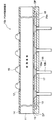
Further, in the example of FIG. 1, the exposed portion of the adhesive 19 filled in the gap between the through hole TH of the
図2に示す各図(a)〜(f)において、上側に示す「接着前」の状態は、一方の面に未硬化状態で接着剤が形成されたピン固定用板の、これとは別工程で用意した所要の配線基板(チップ実装面側と反対側の面に形成されたパッド部にピンのヘッド部をはんだを介して接合した配線基板)に接着する前の断面構造を示しており、下側に示す「接着後」の状態は、当該ピン固定用板を当該配線基板に接着した後の断面構造を示している。 In each of the drawings (a) to (f) shown in FIG. 2, the “before bonding” state shown on the upper side is different from that of the pin fixing plate in which an adhesive is formed on one surface in an uncured state. Shows the cross-sectional structure before bonding to the required wiring board prepared in the process (wiring board in which the head part of the pin is joined to the pad part formed on the surface opposite to the chip mounting surface side via solder) The “after bonding” state shown on the lower side shows a cross-sectional structure after bonding the pin fixing plate to the wiring board.
図2において、(a)及び(b)に示す例では、ピン固定用板20に断面的に見て一定の大きさで貫通孔THを形成し、このピン固定用板20の一方の面に形成される接着剤の使用量を適宜変えたものを用意し(図示の例では、(a)の場合に形成される接着剤19aの使用量と比べて、(b)の場合に形成される接着剤19bの使用量の方が多い)、この接着剤の付いたピン固定用板20の貫通孔THに、これとは別工程で用意した配線基板に接合されているピンの軸部18bを挿通させて、両者を接着している。このようにピン固定用板20に形成すべき接着剤19a,19bの使用量を適宜調整することで、当該接着剤のピンの軸部18bへの這い上がり量(高さ)を変えることができる。
In the example shown in FIGS. 2A and 2B, a through hole TH is formed in the
また、ピン固定用板20の貫通孔THの径をピンのヘッド部18aの径より大きくし、貫通孔TH内にヘッド部18aの突出部分(ソルダレジスト層15の表面から上方に突出するヘッド部18aの部分)が収容されるようにすると、ソルダレジスト層15上のピン固定用板20の高さを低く抑えることができる。これにより、配線基板10全体の薄型化を図ることができるので、有用である。
Further, the diameter of the through hole TH of the
図2(c)及び(d)に示す例では、ピン固定用板21に断面的に見て段差状に2段構成の貫通孔TH1を形成し、上記と同様に、このピン固定用板21の一方の面に形成される接着剤の使用量を適宜変えたものを用意し(図示の例では、(c)の場合に形成される接着剤19cの使用量と比べて、(d)の場合に形成される接着剤19dの使用量の方が多い)、この接着剤の付いたピン固定用板21の貫通孔TH1に、これとは別工程で用意した配線基板に接合されているピンの軸部18bを挿通させて、両者を接着している。この場合も同様に、ピン固定用板21に形成すべき接着剤19c,19dの使用量を調整することで、当該接着剤のピンの軸部18bへの這い上がり量(高さ)を変えることができる。
In the example shown in FIGS. 2C and 2D, the
また、ピン固定用板21に段差状に形成された貫通孔TH1は、ピン固定用板21の、配線基板への接合面側に形成された1段目の段差が、ピンのヘッド部18aの径より大きく開口されており、ピン固定用板21の、配線基板への接合面と反対側の面に形成された2段目の段差が、軸部18bの径より大きく、かつ、ヘッド部18aの径より小さく開口されている。これにより、1段目の段差にヘッド部18aを収容できるので、配線基板全体の薄型化を図ることができ、かつ、ヘッド部18aより小径の2段目の段差により、軸部18bへの接着剤の這い上がりを好適に防止することができる。
Further, the through hole TH1 formed in a step shape in the
図2(e)及び(f)に示す例では、ピン固定用板22に断面的に見てテーパ状に傾斜した部分を含む貫通孔TH2を形成し、上記と同様に、このピン固定用板22の一方の面に形成される接着剤の使用量を適宜変えたものを用意し(図示の例では、(e)の場合に形成される接着剤19eの使用量と比べて、(f)の場合に形成される接着剤19fの使用量の方が多い)、この接着剤の付いたピン固定用板22の貫通孔TH2に、これとは別工程で用意した配線基板に接合されているピンの軸部18bを挿通させて、両者を接着している。この場合も同様に、ピン固定用板22に形成すべき接着剤19e,19fの使用量を調整することで、当該接着剤のピンの軸部18bへの這い上がり量(高さ)を変えることができる。
In the example shown in FIGS. 2 (e) and 2 (f), the
また、ピン固定用板22に形成されたテーパ状の貫通孔TH2は、ピン固定用板22の、配線基板への接合面側に形成されたテーパ部が、接合面側が大径で、接合面側と反対側の面にかけて小径となるような傾斜面を有するテーパに形成されている。そして、ピン固定用板22の、配線基板への接合面側に形成されたテーパ部が、ピンのヘッド部18cを収容できる形状に開口されており、ピン固定用板22の、配線基板への接合面と反対側の面に形成された貫通孔TH2部分が、軸部18bの径より大きく、かつ、ヘッド部18cの径より小さく、かつ、ストレート状に開口されている。これにより、テーパ部にヘッド部18cを収容でき、配線基板全体の薄型化を図れ、かつ、テーパ部より小径のストレート部により、軸部18bへの接着剤の這い上がりを好適に防止できる。その際、ヘッド部18cの軸部18b接合面を、ピン固定用板22のテーパ部形状に合わせ、テーパ面にしておくと、ピン固定用板22により、ヘッド部18cを好適に押さえつけ、固定することができる。
The tapered through hole TH2 formed in the
上述したように、各ピン固定用板20,21,22に形成すべき接着剤19a〜19fの使用量を必要に応じて適宜調整することで、図2(a)〜(f)に示すように当該接着剤のピンの軸部18bへの這い上がり量(高さ)を制御することができるが、この接着剤の這い上がり量(高さ)は、図10(b)に示した「はんだ」の這い上がりの場合と同様に、ピンのヘッド部18a近傍に留めるように制御する必要がある。
As described above, as shown in FIGS. 2A to 2F, the usage amount of the
以下に他の実施形態の幾つかを説明する。 Several other embodiments will be described below.
(第2の実施形態)
図3は本発明の第2の実施形態に係るPGA型配線基板10aの構成を断面図の形態で示したものである。
(Second Embodiment)
FIG. 3 shows the configuration of a PGA
この第2の実施形態に係るPGA型配線基板(半導体パッケージ)10aは、上述した第1の実施形態に係るPGA型配線基板10(図1)の構成と比べて、ピン固定用板21に形成されるピン挿通用の貫通孔TH1の形状及びそれに依存する接着態様(接着剤30の形状)において相違する。他の構成については、第1の実施形態の場合と同様であるのでその説明は省略する。
The PGA type wiring substrate (semiconductor package) 10a according to the second embodiment is formed on the
本実施形態を特徴付ける貫通孔TH1は、図示のように断面的に見て段差状に2段構成で形成されている。そのため、接着剤30(未硬化状態)が形成されたピン固定用板21を配線基板10aに接着すると、図示のように接着剤(層)30の一部が、この段差状の貫通孔TH1の内壁面とピン18(軸部18b)との隙間に充填される。この部分(ピン−基板間接続部)の形態は、上述した図2(c)及び(d)に示した構造に対応している。
The through hole TH1 characterizing the present embodiment is formed in a two-step configuration in a step shape when viewed in cross section as shown in the drawing. Therefore, when the
この第2の実施形態に係るPGA型配線基板10a(図3)の構成によれば、上述した第1の実施形態に係るPGA型配線基板10(図1)において得られた効果に加え、さらに以下の利点が得られる。すなわち、ピン固定用板21に形成される貫通孔TH1が断面的に見て段差状に2段構成で設けられているので、この貫通孔TH1の内壁面に接触する硬化後の接着剤層30の面積を相対的に増やすことができ、この接触面積の大きい接着剤層30の介在により、ピン固定用板21とピン18のヘッド部18a及び軸部18bのヘッド部近傍部分(ピン−基板間接続部)との接着力(接合強度)をより一層高めることが可能となる。
According to the configuration of the PGA
なお、この第2の実施形態では、断面的に見て段差状に2段構成の貫通孔TH1を形成しているが、上述した図2(e)及び(f)に例示したように、断面的に見てテーパ状に傾斜した部分を含むような貫通孔TH2を形成するようにしてもよい。このような構造を採用しても、段差状の貫通孔TH1の場合と同様に接着剤層30の接触面積の拡大化を図ることができるので、同様の作用効果を奏することができる。
In the second embodiment, the through hole TH1 having a two-step configuration is formed in a step shape when viewed in cross section. However, as illustrated in FIGS. 2E and 2F described above, the cross section The through hole TH2 may be formed so as to include a portion inclined in a tapered shape when viewed. Even if such a structure is adopted, the contact area of the
(第3の実施形態)
図4は本発明の第3の実施形態に係るPGA型配線基板10bの構成を断面図の形態で示したものである。
(Third embodiment)
FIG. 4 shows the configuration of a PGA
この第3の実施形態に係るPGA型配線基板(半導体パッケージ)10bは、上述した第1の実施形態に係るPGA型配線基板10(図1)の構成と比べて、本パッケージの周辺部に対応する箇所においてピン固定用板20aにダム部DP(当該部分を「ダム」状に隆起させて成形した部分)を設けた点で相違する。他の構成については、第1の実施形態の場合と同様であるのでその説明は省略する。
The PGA type wiring substrate (semiconductor package) 10b according to the third embodiment corresponds to the peripheral portion of the package as compared with the configuration of the PGA type wiring substrate 10 (FIG. 1) according to the first embodiment described above. The difference is that the
後述するように、接着剤(未硬化状態)が形成されたピン固定用板を所要の配線基板に接着する際、その接着剤を硬化させるために加圧・加熱処理等が行われるが、その際のプロセス条件や使用している接着剤の量によっては、ピン固定用板に形成した接着剤の一部がパッケージ周辺部に流れ出してしまうことも想定される。パッケージの外部に接着剤が流れ出すと、製品(パッケージ)としての外形規格に合わなくなるので、かかる不都合に対処するための方策が必要である。 As will be described later, when a pin fixing plate on which an adhesive (uncured state) is formed is bonded to a required wiring board, pressure and heat treatment are performed to cure the adhesive. Depending on the process conditions at the time and the amount of the adhesive used, it is assumed that a part of the adhesive formed on the pin fixing plate flows out to the periphery of the package. If the adhesive flows out of the package, it will not meet the external standard of the product (package), so a measure for dealing with such inconvenience is required.
そこで、この第3の実施形態では、ピン固定用板20aの周辺部分にリング状にダム部DPを設けることで、接着剤の硬化の際にその一部がパッケージ周辺部に流れ出すのを防止している。このダム部DPは、ピン固定用板20aを構成する基材(例えば、ガラスエポキシ樹脂製の基板)に対しレーザ加工等を施して形成することができる。
Therefore, in the third embodiment, a ring-shaped dam portion DP is provided in the peripheral portion of the
(第4の実施形態)
図5は本発明の第4の実施形態に係るPGA型配線基板10cの構成を断面図の形態で示したものである。
(Fourth embodiment)
FIG. 5 shows a configuration of a PGA type wiring board 10c according to the fourth embodiment of the present invention in the form of a sectional view.
この第4の実施形態に係るPGA型配線基板(半導体パッケージ)10cは、上述した第1の実施形態に係るPGA型配線基板10(図1)の構成と比べて、ピン固定用板20に形成すべき接着剤(層)19を、本パッケージの周辺部に対応する箇所を除いて形成した点で相違する。つまり、接着剤(層)19の形成エリアを、図示のようにパッケージの端部から所定の距離(FRで示す部分)だけパッケージ内部に後退させている。FRで示す部分は、「接着剤の流れ出しのエリア」として規定される。他の構成については、第1の実施形態の場合と同様であるのでその説明は省略する。
The PGA type wiring substrate (semiconductor package) 10c according to the fourth embodiment is formed on the
本実施形態に係るPGA型配線基板10cは、上述した第3の実施形態に係るPGA型配線基板10b(図4)の代替案に相当する。つまり、この第4の実施形態では、ピン固定用板20に形成する接着剤19のエリアを少し小さめにする(その分、パッケージ周辺部に「接着剤の流れ出しのエリアFR」を設ける)ことで、接着剤の硬化の際にその一部がパッケージ周辺部に流れ出しても、このエリアFRで留めるようにしている。
The PGA type wiring board 10c according to the present embodiment corresponds to an alternative to the PGA
(第5の実施形態)
図6は本発明の第5の実施形態に係るPGA型配線基板10dの構成を断面図の形態で示したものである。
(Fifth embodiment)
FIG. 6 shows the configuration of a PGA type wiring board 10d according to the fifth embodiment of the present invention in the form of a sectional view.
この第5の実施形態に係るPGA型配線基板(半導体パッケージ)10dは、上述した第1の実施形態に係るPGA型配線基板10(図1)の構成と比べて、ピン固定用板20の所要の箇所にガス抜き孔GHを多数設けた点で相違する。他の構成については、第1の実施形態の場合と同様であるのでその説明は省略する。
The PGA type wiring substrate (semiconductor package) 10d according to the fifth embodiment is required for the
未硬化状態の接着剤が形成されたピン固定用板を所要の配線基板に接着したときに(本硬化時)、その接着剤から発生するガスにより接着剤層中に空隙(ボイド)が生成されることも想定される。このようなボイドが生じると、接着剤層の劣化(接着強度の低下)をひき起こすといった問題が生じる。 When a pin fixing board on which an uncured adhesive is formed is adhered to a required wiring board (during main curing), voids are generated in the adhesive layer by the gas generated from the adhesive. It is also assumed that. When such a void occurs, there arises a problem of causing deterioration of the adhesive layer (decrease in adhesive strength).
そこで、この第5の実施形態では、ピン固定用板20にガス抜き孔GHを適宜設けることで、接着剤19から発生したガスを効果的に外部に逃している。これによって、ピン固定用板20と配線基板(11〜18)との間に空隙(ボイド)が生成されるのを防止することができる。このようなガス抜き孔GHは、ピン固定用板20を構成する基材に対しレーザ加工等を施して形成することができる。
Therefore, in the fifth embodiment, the gas generated from the adhesive 19 is effectively released to the outside by appropriately providing the vent holes GH in the
(PGA型配線基板の製造方法)
次に、上述した各実施形態に係るPGA型配線基板を製造する方法について説明する。基本となる工程は各製造方法とも実質的に同じであるので、代表として、第2の実施形態に係るPGA型配線基板10a(図3)を製造する方法について説明する。図7及び図8はその製造工程の一例を示したものである。
(Manufacturing method of PGA type wiring board)
Next, a method for manufacturing the PGA type wiring board according to each embodiment described above will be described. Since the basic steps are substantially the same for each manufacturing method, as a representative, a method for manufacturing the PGA
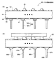
先ず、本工程に入る前に、本発明を特徴付けるピン固定用板(その一方の面に未硬化状態の接着剤が形成されているもの)を接着する前の段階にある配線基板(図8(a)の下側に示す構造体)を用意する。すなわち、配線基板本体を構成する樹脂基板11の両面に所要の形状にパターニング形成された配線層12及び13を有し、各配線層12,13の所要の箇所に画定されたパッド部を除いて両面を覆うように形成された保護膜としての絶縁層14及び15を備え、さらにチップ実装面側のパッド部(配線層12)にはんだ16が被着され、反対側のパッド部(配線層13)にははんだ17を介してピン18のヘッド部18aが接合された配線基板を作製する。
First, before entering this process, a wiring board in a stage before bonding a pin fixing plate (which has an uncured adhesive formed on one surface thereof) characterizing the present invention (FIG. 8 ( a) The structure shown below is prepared. That is, the wiring layers 12 and 13 are patterned and formed in a required shape on both surfaces of the
樹脂基板11の形態としては、上述したように少なくとも最表層に配線層が形成された基板であって、各配線層が基板内部を通して電気的に接続されている形態のものであれば十分である。例えば、ビルドアップ法を用いた多層構造の配線基板を利用することができる。これは、ベース基材としてのコア基板を中心としてその両面に、絶縁層の形成、絶縁層におけるビアホールの形成、ビアホールの内部を含めた配線パターン(配線層)の形成を順次繰り返して積み上げていくものである。絶縁層の材料としては典型的にエポキシ樹脂が用いられ、配線層の材料としては典型的に銅(Cu)が用いられる。かかるプロセスを経て形成された最表層の配線層12,13は、基板内部の所要箇所に適宜形成された各配線層及び各配線層間を相互に接続するビアホールを介して電気的に接続されている。
As the form of the
最表層の配線層12,13の所定の箇所に画定される各パッド部には、外部接続端子が接合されるので、配線層(Cu)12,13上にニッケル(Ni)めっき及び金(Au)めっきをこの順に施しておく。これは、外部接続端子を接合した時のコンタクト性を良くするため(Au層)と、このAu層とパッド部を構成するCu層との密着性を高め、CuがAu層中へ拡散するのを防止するため(Ni層)である。つまり、各パッド部はCu/Ni/Auの3層構造となっている。 Since external connection terminals are joined to the pad portions defined at predetermined positions of the outermost wiring layers 12 and 13, nickel (Ni) plating and gold (Au) are formed on the wiring layers (Cu) 12 and 13. ) Apply plating in this order. This improves the contact property when the external connection terminals are joined (Au layer) and improves the adhesion between the Au layer and the Cu layer constituting the pad portion, so that Cu diffuses into the Au layer. This is to prevent (Ni layer). That is, each pad portion has a three-layer structure of Cu / Ni / Au.
さらに樹脂基板11の両面に、それぞれ保護膜として機能するソルダレジスト層14及び15を形成する。例えば、感光性のエポキシ樹脂を樹脂基板11及び配線層12,13上に塗布し、それぞれ樹脂層を所要の形状(配線層12,13のパッド部を除いた形状)にパターニングすることで、ソルダレジスト層14,15を形成することができる。さらに、樹脂基板11のチップ実装面側のパッド部(配線層12)にプリソルダによりはんだ16を被着させ、その反対側のパッド部(配線層13)に、はんだ17を使用してピン18を接合する。ピン18の接合は、当該パッド部にはんだペーストを塗布し、このパッド部上にピン18のヘッド部18aを当接させ、立設状態を保ったままリフローして行われる。
Further, solder resist
このようにして、ピン固定用板を接着する前の段階にある配線基板を用意した状態で、本工程に入る。 In this way, the present process is entered with the wiring board in a stage before the pin fixing plate is bonded.
先ず最初の工程では(図7(a)参照)、ピン固定用板21(図3参照)を構成する基材として、例えば、大きさが10mm×10mm〜70mm×70mm程度で、厚さが10μm〜800μm程度のガラスエポキシ樹脂製の基板(ビルドアップ配線基板のベース基材として用いられているコア材)を用意する。そして、この基板の所要の箇所に、樹脂基板11の実装面側に設けたピン18の配列に合わせて、それぞれ当該ピン18(軸部18b)を挿通させるための貫通孔TH(その径がピン18の1.1〜1.5倍程度)を形成する。例えば、機械ドリル加工、CO2 レーザやエキシマレーザ等によるレーザ加工、抜き型を用いたプレス加工等により形成することができる。さらに、基材として銅(Cu)、アルミニウム(Al)等の金属板(ただし、その表面に絶縁処理を施したもの)を使用した場合には、エッチング加工によっても貫通孔THを形成することができる。このように基材に対して穴加工を施すことにより、図示のように一定の大きさで貫通孔THが形成されたピン固定用板20が作製されたことになる。
In the first step (see FIG. 7A), as a base material constituting the pin fixing plate 21 (see FIG. 3), for example, the size is about 10 mm × 10 mm to 70 mm × 70 mm and the thickness is 10 μm. A substrate made of glass epoxy resin having a thickness of about 800 μm (a core material used as a base substrate of a build-up wiring substrate) is prepared. Then, through holes TH (the diameter of which is a pin) through which the pins 18 (
なお、第3の実施形態に係るPGA型配線基板10b(図4)については、この工程において、本パッケージの周辺部に対応する箇所にダム部DPを形成することができる。また、第5の実施形態に係るPGA型配線基板10d(図6)については、この工程において、ピン固定用板20の所要の箇所にガス抜き孔GHを形成することができる。
For the PGA
次の工程では(図7(b)参照)、その作製されたピン固定用板20の貫通孔THに対し、その貫通孔THの径よりも大きな一定の径(その径がピン18の1.1〜1.5倍程度)をもって貫通孔THの途中の部分(深さが1/2程度)までを開口する。つまり、断面的に見て段差状に2段構成の貫通孔TH1(図3参照)を形成する。この追加の開口処理は、例えば、機械ドリル加工、フライス加工等により行うことができる。また、基材として金属板を使用している場合にはエッチング加工によっても開口することができる。このように追加の開口処理を施すことにより、図示のように貫通孔TH1が形成されたピン固定用板21が作製されたことになる。
1 of the following, in the process (see FIG. 7 (b)), with respect to the through-hole TH of the fabricated
あるいは、この追加の開口処理(段差状の貫通孔TH1)の変形例として、断面的に見てテーパ状に傾斜した部分を含むような貫通孔TH2(ピン固定用板22)を形成するようにしてもよい。この場合も、上記と同様の加工処理によって開口することができる。すなわち、その作製されたピン固定用板20の貫通孔THに対し、その貫通孔THの径よりも大きな径をもってテーパ状に貫通孔THの途中の部分(深さが1/2程度)までを開口する。
Alternatively, as a modification of this additional opening process (stepped through hole TH1), a through hole TH2 (pin fixing plate 22) including a portion inclined in a taper shape when viewed in cross section is formed. May be. Also in this case, the opening can be made by the same processing as described above. That is, with respect to the through-hole TH of the
次の工程では(図7(c)参照)、ピン固定用板21に貼付すべき接着剤(層)30を用意する。先ず、接着剤層30を構成する材料として、未硬化状態(Bステージ状態)のエポキシ樹脂、アクリル樹脂等からなるフィルム状の接着剤30(厚さが5〜300μm程度)を用意する。次に、このフィルム状の接着剤30に、ピン固定用板21に形成した貫通孔TH1の配列(すなわち、ピン18の配列)に合わせて、開口部OPを形成する。この開口部OPの大きさは、少なくとも、ピン固定用板21に形成した貫通孔TH1の径の大きい方の側(図示の例では、上側)の大きさに選定されている。開口部OPは、例えば、機械ドリル加工、レーザ加工、抜き型を用いたプレス加工等により形成することができる。
In the next step (see FIG. 7C), an adhesive (layer) 30 to be attached to the
次の工程では(図7(d)参照)、貫通孔TH1が形成されたピン固定用板21の一方の面(貫通孔TH1の径の大きい方の側の面)に、貫通孔TH1の位置に開口部OPの位置を合わせて接着剤(層)30を仮付けする。その際、接着剤30の本硬化温度(120〜180℃前後)よりも低い温度(50〜110℃前後)で仮付けする。
In the next step (see FIG. 7 (d)), the position of the through hole TH1 on one surface of the
次の工程では(図8(a)参照)、ピン固定用板21の接着剤層30(未硬化状態)が貼付されている側の面を、これとは別工程であらかじめ用意した配線基板(図中、下側に示す構造体:11〜18)のピン18が接合されている側の面に対向させ、ピン18の軸部18bをそれぞれ対応する貫通孔TH1に挿通させて、対向する両面を当接させる。
In the next step (see FIG. 8A), the surface of the
次の工程では(図8(b)参照)、対向する両面が当接されたピン固定用板21(未硬化状態の接着剤層30)と配線基板10aとを、プレス40により加圧し、更に20〜180℃前後の温度で加熱して、接着する。その加熱の際、接着剤層30は硬化して、図示のようにピン18のヘッド部18aの周囲を覆い、さらにピン固定用板21の貫通孔TH1とピン18の軸部18bとの隙間を充填する。このとき、図8(b)には明示していないが、接着剤層30の接着剤は貫通孔TH1内からピン18の軸部18b上にわずかに這い上がる。
In the next step (see FIG. 8 (b)), the pin fixing plate 21 (uncured adhesive layer 30) and the
以上の工程により、第2の実施形態に係るPGA型配線基板10a(図3)が製造されたことになる。
Through the above steps, the PGA
上述したプロセスでは、フィルム状の樹脂を用いて接着剤層30を形成した場合を例にとって説明したが、使用する材料がフィルム状のものに限定されないことはもちろんであり、液状(ペースト状)の樹脂を使用することも可能である。図9は、その場合の幾つかの方法を簡略化して示したものである。
In the above-described process, the case where the
基本的なプロセスは、先ず、所要の箇所に貫通孔TH1が形成されたピン固定用板21の一方の面に、図9(a1)、(a2)又は(a3)に示した方法により、液状もしくはペースト状の樹脂(エポキシ樹脂、アクリル樹脂等)を塗布し、次に、図9(b)に示すように、その塗布された樹脂(接着剤30)を仮乾燥させる。その際、接着剤30の本硬化温度よりも低い温度で仮乾燥させる。これによって、図7(d)に示したものと同等の構造体が出来上がる。
The basic process is as follows. First, a liquid is applied to one surface of a
図9(a1)に示す例では、スクリーン印刷法により樹脂を塗布している。すなわち、樹脂基板11に設けたピン18の配列に合わせてその配列部(貫通孔TH1に対応する箇所)を隠すようにパターニングされたマスク51をピン固定用板21上に配置し、スキージー52を用いて、樹脂ペースト30aをマスク51の開口部に押し出してピン固定用板21上に塗布する。また、図9(a2)に示す例では、液状の樹脂(接着剤30b)の入ったディスペンサ53を用いて、そのノズルから適量の樹脂30bをピン固定用板21上に塗布している。また、図9(a3)に示す例では、ピン固定用板21上に向けてシャワー54から液状の樹脂(接着剤30c)を噴霧することで塗布している。その際、樹脂は霧状に散布されるので、ピン固定用板21の塗布対象面と反対側の面と側面に保護シート55を貼り付けておくことで、不要な樹脂が付かないようにする。
In the example shown in FIG. 9 (a1), the resin is applied by a screen printing method. That is, the
上述した各実施形態においては、本発明を特徴付けるピン固定用板(その一方の面に未硬化状態の接着剤が形成されているもの)を接着する前の段階にある配線基板の形態として樹脂基板11を使用した場合を例にとって説明したが、本発明の要旨からも明らかなように、樹脂基板に限定されないことはもちろんである。例えば、CSP(チップサイズパッケージ)において用いられているようなシリコン基板の形態であってもよい。この形態の場合には、上記の配線層12,13の所要の箇所に画定されたパッド部の代わりに、シリコン(Si)基板上にアルミニウム(Al)の電極パッドが設けられ、上記のソルダレジスト層14,15の代わりに、SiO2 、SiN、ポリイミド樹脂等からなるパッシベーション膜が設けられる。
In each of the above-described embodiments, a resin substrate is used as a form of the wiring board in a stage before bonding the pin fixing plate characterizing the present invention (one having an uncured adhesive formed on one surface thereof). 11 is used as an example. However, as is apparent from the gist of the present invention, it is needless to say that the present invention is not limited to a resin substrate. For example, it may be in the form of a silicon substrate as used in CSP (chip size package). In the case of this embodiment, instead of the pad portion defined at a required portion of the wiring layers 12 and 13, an electrode pad of aluminum (Al) is provided on a silicon (Si) substrate, and the solder resist described above is provided. Instead of the
10,10a,10b,10c,10d…PGA型配線基板、
11…樹脂基板(配線基板本体)、
12,13…配線層(パッド部)、
14,15…ソルダレジスト層(保護膜/絶縁層)、
16,17…はんだ、
18…ピン(外部接続端子)、
18a,18c…(ピンの)ヘッド部、
18b…(ピンの)軸部、
19,19a,19b,19c,19d,19e,19f,30…接着剤(層)、
20,20a,21,22…ピン固定用板、
DP…ダム部、
FR…接着剤の流れ出しのエリア、
GH…ガス抜き孔、
TH,TH1,TH2…貫通孔。
10, 10a, 10b, 10c, 10d ... PGA type wiring board,
11 ... Resin substrate (wiring board body),
12, 13 ... wiring layer (pad part),
14, 15 ... Solder resist layer (protective film / insulating layer),
16, 17 ... solder,
18 ... pin (external connection terminal),
18a, 18c ... (pin) head part,
18b ... (pin) shaft,
19, 19a, 19b, 19c, 19d, 19e, 19f, 30 ... adhesive (layer),
20, 20a, 21, 22 ... Pin fixing plate,
DP ... Dam section,
FR ... Adhesive flow area,
GH ... vent hole,
TH, TH1, TH2 ... through holes.
Claims (18)
ヘッド部及び該ヘッド部に接合された軸部を有するピンと、
貫通孔が形成されたピン固定用板とを備え、
前記ピンのヘッド部が、導電性材料を介して前記パッド部に接合され、
前記ピン固定用板が、接着剤層を介して前記配線基板の表面に接着され、
前記貫通孔に前記ピンの軸部が挿通されると共に、前記接着剤層の接着剤が、前記貫通孔と前記軸部との隙間に充填され、且つ前記軸部上を前記貫通孔の外まで這い上がっていることを特徴とするPGA型配線基板。 A wiring board having a pad portion formed on the surface;
A pin having a head portion and a shaft portion joined to the head portion;
A pin fixing plate with a through hole formed therein,
The head portion of the pin is bonded to the pad portion via a conductive material,
The pin fixing plate is bonded to the surface of the wiring board via an adhesive layer,
The shaft portion of the pin is inserted into the through-hole, and the adhesive of the adhesive layer is filled in the gap between the through-hole and the shaft portion, and the shaft portion is extended to the outside of the through-hole. A PGA type wiring board characterized by crawling up.
前記ピン固定用板が、前記接着剤層を介して前記ソルダレジスト層に接着され、
前記貫通孔に前記ピンの軸部が挿通されると共に、前記ソルダレジスト層の表面から突出する前記ヘッド部の部分が、前記貫通孔内に収容されていることを特徴とする請求項1に記載のPGA型配線基板。 A solder resist layer is provided by exposing the pad portion on the surface of the wiring board,
The pin fixing plate is bonded to the solder resist layer through the adhesive layer,
2. The shaft portion of the pin is inserted into the through hole, and a portion of the head portion protruding from the surface of the solder resist layer is accommodated in the through hole. PGA type wiring board.
貫通孔が形成されたピン固定用板を作製する工程と、
前記ピン固定用板の一方の面に未硬化状態の接着剤層を形成する工程と、
前記配線基板の前記ピンが接合されている側の面に前記ピン固定用板の前記接着剤層が形成されている側の面を対向させ、当該ピンのヘッド部に接合された軸部を前記貫通孔に挿通させて対向する両面を当接させる工程と、
前記接着剤層を、その接着剤が前記貫通孔と前記軸部との隙間を充填し、且つ前記軸部上を前記貫通孔の外まで這い上がるように硬化させて、前記配線基板に前記ピン固定用板を接着する工程とを含むことを特徴とするPGA型配線基板の製造方法。 A step of preparing a wiring board in which a pad portion is formed on a surface and a head portion of a pin is bonded to the pad portion via a conductive material;
Producing a pin fixing plate in which a through hole is formed;
Forming an uncured adhesive layer on one surface of the pin fixing plate;
The surface of the wiring board where the pin is bonded is opposed to the surface of the pin fixing plate where the adhesive layer is formed, and the shaft portion bonded to the head portion of the pin is A step of passing through the through-hole and bringing the opposing surfaces into contact with each other;
The adhesive layer is hardened so that the adhesive fills a gap between the through hole and the shaft portion and crawls up to the outside of the through hole on the shaft portion , and the pin is attached to the wiring board. A method of manufacturing a PGA type wiring board, comprising the step of adhering a fixing plate.
前記配線基板に前記ピン固定用板を接着する工程において、該ピン固定用板を前記接着剤層を介して前記ソルダレジスト層に接着すると共に、前記ピンのヘッド部の部分を前記貫通孔内に収容することを特徴とする請求項9に記載のPGA型配線基板の製造方法。 In the step of preparing the wiring substrate, the pad portion is exposed on the surface of the wiring substrate to form a solder resist layer, and the head portion of the pin protrudes from the surface of the solder resist layer. Bond to the pad,
In the step of bonding the pin fixing plate to the wiring board, the pin fixing plate is bonded to the solder resist layer through the adhesive layer, and the head portion of the pin is placed in the through hole. The method for manufacturing a PGA type wiring board according to claim 9, wherein the PGA type wiring board is housed .
Priority Applications (3)
| Application Number | Priority Date | Filing Date | Title |
|---|---|---|---|
| JP2008041441A JP4993754B2 (en) | 2008-02-22 | 2008-02-22 | PGA type wiring board and manufacturing method thereof |
| US12/372,870 US20090211798A1 (en) | 2008-02-22 | 2009-02-18 | Pga type wiring board and method of manufacturing the same |
| KR1020090014481A KR101521485B1 (en) | 2008-02-22 | 2009-02-20 | Pga type wiring board and mehtod of manufacturing the same |
Applications Claiming Priority (1)
| Application Number | Priority Date | Filing Date | Title |
|---|---|---|---|
| JP2008041441A JP4993754B2 (en) | 2008-02-22 | 2008-02-22 | PGA type wiring board and manufacturing method thereof |
Publications (3)
| Publication Number | Publication Date |
|---|---|
| JP2009200313A JP2009200313A (en) | 2009-09-03 |
| JP2009200313A5 JP2009200313A5 (en) | 2011-03-31 |
| JP4993754B2 true JP4993754B2 (en) | 2012-08-08 |
Family
ID=40997206
Family Applications (1)
| Application Number | Title | Priority Date | Filing Date |
|---|---|---|---|
| JP2008041441A Active JP4993754B2 (en) | 2008-02-22 | 2008-02-22 | PGA type wiring board and manufacturing method thereof |
Country Status (3)
| Country | Link |
|---|---|
| US (1) | US20090211798A1 (en) |
| JP (1) | JP4993754B2 (en) |
| KR (1) | KR101521485B1 (en) |
Families Citing this family (9)
| Publication number | Priority date | Publication date | Assignee | Title |
|---|---|---|---|---|
| JP5290017B2 (en) * | 2008-03-28 | 2013-09-18 | 日本特殊陶業株式会社 | Multilayer wiring board and manufacturing method thereof |
| JP5079646B2 (en) * | 2008-08-26 | 2012-11-21 | 新光電気工業株式会社 | Semiconductor package, manufacturing method thereof, and semiconductor device |
| US20110147069A1 (en) * | 2009-12-18 | 2011-06-23 | International Business Machines Corporation | Multi-tiered Circuit Board and Method of Manufacture |
| JP2012164965A (en) * | 2011-01-21 | 2012-08-30 | Ngk Spark Plug Co Ltd | Wiring board and manufacturing method of the same |
| JP2012169591A (en) * | 2011-01-24 | 2012-09-06 | Ngk Spark Plug Co Ltd | Multilayer wiring board |
| JP6008582B2 (en) * | 2012-05-28 | 2016-10-19 | 新光電気工業株式会社 | Semiconductor package, heat sink and manufacturing method thereof |
| TW201432961A (en) * | 2013-02-05 | 2014-08-16 | Lextar Electronics Corp | Substrate structure |
| CN106211629B (en) * | 2016-08-30 | 2018-10-02 | 无锡市同步电子制造有限公司 | The method that high-temperature soldering is carried out in printed circuit board processing |
| US11808787B2 (en) * | 2020-08-28 | 2023-11-07 | Unimicron Technology Corp. | Probe card testing device |
Family Cites Families (22)
| Publication number | Priority date | Publication date | Assignee | Title |
|---|---|---|---|---|
| JPH01313969A (en) * | 1988-06-13 | 1989-12-19 | Hitachi Ltd | Semiconductor device |
| US5103292A (en) * | 1989-11-29 | 1992-04-07 | Olin Corporation | Metal pin grid array package |
| US5261157A (en) * | 1991-01-22 | 1993-11-16 | Olin Corporation | Assembly of electronic packages by vacuum lamination |
| JP2658672B2 (en) * | 1991-10-11 | 1997-09-30 | 日本電気株式会社 | I / O pin repair structure and repair method |
| JPH05183019A (en) * | 1991-12-27 | 1993-07-23 | Hitachi Ltd | Semiconductor device and manufacture thereof |
| US6835898B2 (en) * | 1993-11-16 | 2004-12-28 | Formfactor, Inc. | Electrical contact structures formed by configuring a flexible wire to have a springable shape and overcoating the wire with at least one layer of a resilient conductive material, methods of mounting the contact structures to electronic components, and applications for employing the contact structures |
| JPH09102560A (en) * | 1995-10-05 | 1997-04-15 | Sumitomo Kinzoku Electro Device:Kk | External lead pin joining structure for low-temperature baked ceramic substrate |
| JP3037885B2 (en) * | 1995-10-31 | 2000-05-08 | 日本特殊陶業株式会社 | Substrate for PGA type electronic components |
| JPH09213836A (en) * | 1996-02-07 | 1997-08-15 | Sumitomo Kinzoku Electro Device:Kk | Low temperature fired ceramic package |
| US5952716A (en) * | 1997-04-16 | 1999-09-14 | International Business Machines Corporation | Pin attach structure for an electronic package |
| JP4046854B2 (en) * | 1998-06-29 | 2008-02-13 | イビデン株式会社 | Method for manufacturing printed wiring board with pins |
| JP2000058736A (en) * | 1998-08-07 | 2000-02-25 | Sumitomo Kinzoku Electro Device:Kk | Pin connection method to resin substrate |
| KR20080043408A (en) * | 1998-12-16 | 2008-05-16 | 이비덴 가부시키가이샤 | Conductive connecting pin and package board |
| US20020019168A1 (en) * | 1999-01-12 | 2002-02-14 | Robert W. Hooley | Pin array header with floating surface mount interconnects |
| US6217346B1 (en) * | 1999-05-11 | 2001-04-17 | Illinois Tool Works Inc. | Solderless pin connection |
| US6830460B1 (en) * | 1999-08-02 | 2004-12-14 | Gryphics, Inc. | Controlled compliance fine pitch interconnect |
| US6974765B2 (en) * | 2001-09-27 | 2005-12-13 | Intel Corporation | Encapsulation of pin solder for maintaining accuracy in pin position |
| AU2003230696A1 (en) * | 2002-03-20 | 2003-10-08 | Andrew Corporation | Interconnection pin/socket components for electrically connecting two circuit boards and method for mounting said components in a circuit board |
| JP4054269B2 (en) * | 2003-03-20 | 2008-02-27 | Tdk株式会社 | Electronic component manufacturing method and electronic component |
| US7887899B2 (en) * | 2005-08-25 | 2011-02-15 | Sumitomo Electric Industries, Ltd. | Anisotropic conductive sheet, production method thereof, connection method and inspection method |
| TWI298613B (en) * | 2006-05-19 | 2008-07-01 | Foxconn Advanced Tech Inc | Method for manufacturing via holes used in printed circuit boards |
| US20080192446A1 (en) * | 2007-02-09 | 2008-08-14 | Johannes Hankofer | Protection For Circuit Boards |
-
2008
- 2008-02-22 JP JP2008041441A patent/JP4993754B2/en active Active
-
2009
- 2009-02-18 US US12/372,870 patent/US20090211798A1/en not_active Abandoned
- 2009-02-20 KR KR1020090014481A patent/KR101521485B1/en active IP Right Grant
Also Published As
| Publication number | Publication date |
|---|---|
| JP2009200313A (en) | 2009-09-03 |
| KR20090091070A (en) | 2009-08-26 |
| US20090211798A1 (en) | 2009-08-27 |
| KR101521485B1 (en) | 2015-05-20 |
Similar Documents
| Publication | Publication Date | Title |
|---|---|---|
| JP4993754B2 (en) | PGA type wiring board and manufacturing method thereof | |
| JP3875077B2 (en) | Electronic device and device connection method | |
| JP4928945B2 (en) | Bump-on-lead flip chip interconnect | |
| JP5113114B2 (en) | Wiring board manufacturing method and wiring board | |
| US8101866B2 (en) | Packaging substrate with conductive structure | |
| KR20030067590A (en) | Semiconductor element and a producing method for the same, and a semiconductor device and a producing method for the same | |
| TWI492677B (en) | Wiring board and method of manufacturing the same | |
| US20040235287A1 (en) | Method of manufacturing semiconductor package and method of manufacturing semiconductor device | |
| US8779300B2 (en) | Packaging substrate with conductive structure | |
| JP2006005322A (en) | Part mounting wiring board and method for mounting part to wiring board | |
| JP4918780B2 (en) | Multilayer wiring board manufacturing method and semiconductor device | |
| JP4051570B2 (en) | Manufacturing method of semiconductor device | |
| JP4835629B2 (en) | Manufacturing method of semiconductor device | |
| WO2007080863A1 (en) | Semiconductor device, printed wiring board mounted with such semiconductor device, and connection structure for those | |
| JP2019021752A (en) | Wiring board, electronic equipment, method of manufacturing wiring board and method of manufacturing electronic equipment | |
| JP5541157B2 (en) | Mounting substrate, substrate, and manufacturing method thereof | |
| JP4429435B2 (en) | Bumped double-layer circuit tape carrier and manufacturing method thereof | |
| JP4045708B2 (en) | Semiconductor device, electronic circuit device and manufacturing method | |
| JP4065264B2 (en) | Substrate with relay substrate and method for manufacturing the same | |
| JP3742732B2 (en) | Mounting board and mounting structure | |
| JP2016127066A (en) | Printed wiring board with bump and manufacturing method of the same | |
| JP2004200608A (en) | Printed wiring board, and manufacturing method thereof | |
| US20230276575A1 (en) | Embedded printed circuit board | |
| TWI550738B (en) | Surface mounting integrated circuit components | |
| JP2011238843A (en) | Wiring board with bump electrode and method for manufacturing the same |
Legal Events
| Date | Code | Title | Description |
|---|---|---|---|
| A521 | Written amendment |
Free format text: JAPANESE INTERMEDIATE CODE: A523 Effective date: 20110208 |
|
| A621 | Written request for application examination |
Free format text: JAPANESE INTERMEDIATE CODE: A621 Effective date: 20110208 |
|
| A977 | Report on retrieval |
Free format text: JAPANESE INTERMEDIATE CODE: A971007 Effective date: 20111020 |
|
| A131 | Notification of reasons for refusal |
Free format text: JAPANESE INTERMEDIATE CODE: A131 Effective date: 20111025 |
|
| A521 | Written amendment |
Free format text: JAPANESE INTERMEDIATE CODE: A523 Effective date: 20111205 |
|
| TRDD | Decision of grant or rejection written | ||
| A01 | Written decision to grant a patent or to grant a registration (utility model) |
Free format text: JAPANESE INTERMEDIATE CODE: A01 Effective date: 20120501 |
|
| A01 | Written decision to grant a patent or to grant a registration (utility model) |
Free format text: JAPANESE INTERMEDIATE CODE: A01 |
|
| A61 | First payment of annual fees (during grant procedure) |
Free format text: JAPANESE INTERMEDIATE CODE: A61 Effective date: 20120507 |
|
| FPAY | Renewal fee payment (event date is renewal date of database) |
Free format text: PAYMENT UNTIL: 20150518 Year of fee payment: 3 |
|
| R150 | Certificate of patent or registration of utility model |
Free format text: JAPANESE INTERMEDIATE CODE: R150 Ref document number: 4993754 Country of ref document: JP Free format text: JAPANESE INTERMEDIATE CODE: R150 |