JP4936333B2 - Vacuum deposition equipment - Google Patents
Vacuum deposition equipment Download PDFInfo
- Publication number
- JP4936333B2 JP4936333B2 JP2007250735A JP2007250735A JP4936333B2 JP 4936333 B2 JP4936333 B2 JP 4936333B2 JP 2007250735 A JP2007250735 A JP 2007250735A JP 2007250735 A JP2007250735 A JP 2007250735A JP 4936333 B2 JP4936333 B2 JP 4936333B2
- Authority
- JP
- Japan
- Prior art keywords
- film thickness
- substrate
- correction plate
- rotation axis
- thickness correction
- Prior art date
- Legal status (The legal status is an assumption and is not a legal conclusion. Google has not performed a legal analysis and makes no representation as to the accuracy of the status listed.)
- Active
Links
- 238000001771 vacuum deposition Methods 0.000 title claims description 6
- 239000000758 substrate Substances 0.000 claims description 80
- 238000001704 evaporation Methods 0.000 claims description 15
- 230000008020 evaporation Effects 0.000 claims description 14
- 230000002093 peripheral effect Effects 0.000 claims description 13
- 239000000463 material Substances 0.000 claims description 8
- 238000007738 vacuum evaporation Methods 0.000 claims description 5
- 238000000151 deposition Methods 0.000 claims description 3
- 230000008021 deposition Effects 0.000 claims description 3
- 238000000926 separation method Methods 0.000 claims description 2
- 230000015572 biosynthetic process Effects 0.000 description 16
- 238000009826 distribution Methods 0.000 description 13
- 238000007740 vapor deposition Methods 0.000 description 12
- 230000007246 mechanism Effects 0.000 description 10
- 238000000034 method Methods 0.000 description 4
- 230000006866 deterioration Effects 0.000 description 3
- 238000010438 heat treatment Methods 0.000 description 2
- 230000006872 improvement Effects 0.000 description 2
- 230000008901 benefit Effects 0.000 description 1
- 230000008859 change Effects 0.000 description 1
- 230000007423 decrease Effects 0.000 description 1
- 238000010894 electron beam technology Methods 0.000 description 1
- 239000011521 glass Substances 0.000 description 1
- 238000012423 maintenance Methods 0.000 description 1
- 238000004519 manufacturing process Methods 0.000 description 1
- 239000002245 particle Substances 0.000 description 1
- 238000003892 spreading Methods 0.000 description 1
- 230000007480 spreading Effects 0.000 description 1
- 238000004544 sputter deposition Methods 0.000 description 1
- 230000001360 synchronised effect Effects 0.000 description 1
Images


Description
本発明は真空蒸着装置に関し、特に、真空蒸着装置の膜厚補正のための機構の改良に関する。 The present invention relates to a vacuum deposition apparatus, and more particularly to an improvement in a mechanism for correcting a film thickness of the vacuum deposition apparatus.
基板ドームと呼ばれる基板保持具と蒸発源の間に膜厚補正板を配置し、基板ドームの回転手段により膜厚分布を補正する成膜方法が従来から一般的に用いられている。特許文献1には、更に補正体が基板ドームと同一または逆方向に回転する成膜方法が開示されている。 A film forming method in which a film thickness correction plate is arranged between a substrate holder called a substrate dome and an evaporation source, and the film thickness distribution is corrected by rotating means of the substrate dome has been generally used. Patent Document 1 further discloses a film forming method in which the correction body rotates in the same direction as the substrate dome or in the opposite direction.
上記構成による膜厚分布補正は、回転軸に近いほど精度を得難いという課題がある。これは、回転円周が小さいほど膜厚補正板の寸法が分布精度に与える影響が大きいためである。また、回転の中心に着目すると、膜厚補正板が蒸発源を常に遮蔽するか常に露出するかのどちらかであり、回転の中心が周辺に比して極端に厚膜もしくは極端に薄膜となってしまうという課題もある。そこで従来、基板ドームの回転の中心は実基板の成膜領域としては使用せず、モニタガラスを配置する等して利用していた。 The film thickness distribution correction according to the above configuration has a problem that it is difficult to obtain accuracy as it is closer to the rotation axis. This is because the influence of the dimension of the film thickness correction plate on the distribution accuracy increases as the rotation circumference decreases. Focusing on the center of rotation, either the film thickness correction plate always shields the evaporation source or is always exposed, and the center of rotation is extremely thick or extremely thin compared to the periphery. There is also a problem that it ends up. Therefore, conventionally, the center of rotation of the substrate dome is not used as a film formation region of the actual substrate, but is used by arranging a monitor glass.
このため、大型基板の成膜には巨大な基板ドームを準備する必要があり、これに基板を搭載して成膜を行うため、成膜装置が大型化してしまうという問題があった。例えば、直径1mのドーム状大型基板を成膜するためには幅3〜4mの大型真空槽が必要となり、コスト高となるばかりでなく、真空引きに長時間を要する生産性の低い装置となっていた。 For this reason, it is necessary to prepare a huge substrate dome for film formation of a large substrate, and there is a problem that the film formation apparatus becomes large because the substrate is mounted on this to form a film. For example, in order to form a dome-shaped large substrate having a diameter of 1 m, a large vacuum tank with a width of 3 to 4 m is required, which not only increases the cost, but also results in a low productivity device that requires a long time for evacuation. It was.
蒸発源の直上に一枚板の基板を配置して基板を回転させると、回転軸位置における膜厚分布が極端に悪化して所望の特性を得ることができない、という上記課題に取り組む他の発明として、特許文献2が開示される。特許文献2は、基板の回転軸に対応する部分の近傍に、成膜時に粒子線が基板上に生ずる膜厚補正板の半影の拡がりの半分以下の間隔で配置された複数の開口(メッシュ)と、周辺部に半径方向に開口率が制御された開口とを有する成膜装置である。
特許文献2に開示される成膜装置は、半影の拡がりによって滑らかな分布を生じさせるため、回転軸位置における極端な膜厚分布の悪化を低減することができるが、以下に示すような課題がある。
Since the film forming apparatus disclosed in
半影の拡がりの半分以下の間隔で複数の開口を有するメッシュを形成するためには、極めて狭いピッチ間隔で微小な開口を配列する必要がある。開口の精度はそのまま膜厚分布に反映されるため、補正の都度、開口形成に加工精度が要求される。実施例には、一辺1.8mmの正方形状の開口を2mmピッチで格子状にメッシュを形成することが記載されているが、実際に加工精度を保つことは容易ではない。また、メッシュには成膜により膜が堆積するため、加工精度を保って開口形成しても堆積膜により開口の大きさが変化してしまうという量産性能上の課題もある。 In order to form a mesh having a plurality of openings at intervals less than half the extent of the penumbra, it is necessary to arrange minute openings at extremely narrow pitch intervals. Since the accuracy of the aperture is directly reflected in the film thickness distribution, processing accuracy is required for forming the aperture every time correction is performed. In the embodiment, it is described that a square-shaped opening having a side of 1.8 mm is formed in a grid shape at a pitch of 2 mm, but it is not easy to actually maintain the processing accuracy. Further, since a film is deposited on the mesh by film formation, there is a problem in mass production performance that even if the opening is formed while maintaining processing accuracy, the size of the opening changes depending on the deposited film.
更に、半影の拡がりは膜厚補正板の板厚が厚くなるほど狭くなるので、板厚は薄くせざるを得ない。実施例においても板厚0.5mmの膜厚補正板を用いているが、薄い膜厚補正板に膜が堆積すれば、膜応力や温度上昇で膜厚補正板が変形してしまうという問題が発生する。膜厚補正板の変形はそのまま膜厚分布精度の悪化に直結するため、膜厚補正板の強度は重要な要件である。特許文献2に開示の膜厚補正板は、形成のみでなく形状維持についても課題があり、所望の膜厚分布を得ることが困難であった。
Further, since the spread of the penumbra becomes narrower as the thickness of the film thickness correction plate increases, the plate thickness must be reduced. In the embodiment, a thickness correction plate having a thickness of 0.5 mm is used. However, if a film is deposited on a thin thickness correction plate, there is a problem that the thickness correction plate is deformed due to film stress or temperature rise. appear. Since the deformation of the film thickness correction plate directly affects the deterioration of the film thickness distribution accuracy, the strength of the film thickness correction plate is an important requirement. The film thickness correction plate disclosed in
本発明は、真空蒸着装置において、基板の回転の中心位置であっても膜厚分布を容易に制御可能な装置および方法を提供することを目的とする。 An object of the present invention is to provide an apparatus and a method that can easily control the film thickness distribution even in the center position of the rotation of the substrate in the vacuum deposition apparatus.
本発明の第1の側面は、蒸着材料を蒸発させる蒸発源、第1の回転軸に対して回転され蒸発源に対して対向配置される回転基板、及び第2の回転軸に対して回転され回転基板を蒸発源から部分的に遮蔽する回転膜厚補正板を備えた真空蒸着装置において、第2の回転軸が、回転基板の周縁内に第1の回転軸と離隔して規定された真空蒸着装置である。 The first aspect of the present invention includes an evaporation source that evaporates the vapor deposition material, a rotating substrate that is rotated with respect to the first rotation axis and disposed opposite to the evaporation source, and is rotated with respect to the second rotation axis. In a vacuum deposition apparatus provided with a rotating film thickness correction plate that partially shields the rotating substrate from the evaporation source, the second rotating shaft is defined in the periphery of the rotating substrate so as to be separated from the first rotating shaft. It is a vapor deposition device.
ここで、回転膜厚補正板における第2の回転軸から先端部までの水平距離をL、回転膜厚補正板における第2の回転軸と第1の回転軸との離隔水平距離をX、第1の回転軸から回転基板の周縁部までの水平距離をRとした場合、L≧X+Rとなるようにした。 Here, the horizontal distance from the second rotation axis to the tip of the rotating film thickness correction plate is L, the separation horizontal distance between the second rotation axis and the first rotation axis in the rotating film thickness correction plate is X, the first When the horizontal distance from the rotation axis of 1 to the peripheral edge of the rotating substrate is R, L ≧ X + R.
さらに、回転基板の周縁部を蒸発源から覆うように真空蒸着装置内に固定された固定膜厚補正板を備えてもよい。
ここで、固定膜厚補正板の先端部から回転基板の周縁部までの水平距離をL1、回転膜厚補正板における第2の回転軸から先端部までの水平距離をL2、回転膜厚補正板における第2の回転軸と第1の回転軸との離隔水平距離をX、第1の回転軸から回転基板の周縁部までの水平距離をRとした場合、L1<R、X<L2<R、及び、L1+L2≧X+Rとなるようにした。
Furthermore, you may provide the fixed film thickness correction plate fixed in the vacuum evaporation system so that the peripheral part of a rotation board may be covered from an evaporation source.
Here, the horizontal distance from the tip of the fixed film thickness correction plate to the peripheral edge of the rotating substrate is L 1 , the horizontal distance from the second rotation axis to the tip of the rotating film thickness correction plate is L 2 , and the rotating film thickness is When the horizontal distance between the second rotation axis and the first rotation axis on the correction plate is X, and the horizontal distance from the first rotation axis to the peripheral edge of the rotation substrate is R, L 1 <R, X < L 2 <R and L 1 + L 2 ≧ X + R were satisfied.
本発明の膜厚補正板を用いれば、蒸発源の直上で一枚板の基板を、その内部を通る軸を中心として回転させても回転中心の膜厚を均一化することができる。これにより、(従来では基板中心付近以外を有効な成膜領域として、基板中心付近を不使用領域としていたのに対して)基板のほぼ全域を有効な成膜領域として使用できるので、同じ面積の成膜領域を確保するのに従来よりも小さい基板を用いることができ、その結果として装置全体を小型化することができる。基板ドームに複数枚の基板を搭載する場合であっても同様に、基板ドームの回転中心付近を有効な成膜領域として使用することができるため、生産性の向上若しくは装置の小型化に貢献できる。 If the film thickness correction plate of the present invention is used, the film thickness at the center of rotation can be made uniform even if a single substrate is rotated about an axis passing through the substrate directly above the evaporation source. As a result, the entire area of the substrate can be used as an effective film formation region (as opposed to the conventional film formation region other than the vicinity of the substrate center as an effective film formation region and the substrate center vicinity as an unused region). A substrate smaller than the conventional one can be used to secure the film formation region, and as a result, the entire apparatus can be miniaturized. Similarly, even when a plurality of substrates are mounted on the substrate dome, the vicinity of the rotation center of the substrate dome can be used as an effective film formation region, which can contribute to improvement in productivity or downsizing of the apparatus. .
また、基板中心付近にメッシュ等の特殊な構成を設ける必要がないので膜厚補正板の形成が容易である。そして、膜厚補正板の厚みが成膜精度に直接影響を与えない構成であるので板厚を厚くでき、蒸着物の堆積による変形を防止して膜厚制御の精度を維持することができる。 Further, since it is not necessary to provide a special structure such as a mesh near the center of the substrate, it is easy to form a film thickness correction plate. Further, since the thickness of the film thickness correction plate does not directly affect the film forming accuracy, the plate thickness can be increased, and deformation due to the deposition of the deposit can be prevented and the accuracy of film thickness control can be maintained.
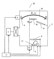
以下、本発明の一実施形態に係る成膜装置および成膜方法を、図1に示す蒸着装置1を参照して説明する。蒸着装置1は、真空槽2、真空ポンプなどの排気装置3、基板保持具4、基板保持具4の回転機構5、蒸発源である坩堝6、蒸着材料21が充填される坩堝6内に電子ビームを照射する電子銃7、坩堝6の遮蔽または露出手段であるシャッタ8、膜厚補正板9、膜厚補正板9の回転機構10、および制御部11を備える。成膜に際しては基板保持具4に基板20を載置し、坩堝6に蒸着材料21を充填する。
Hereinafter, a film forming apparatus and a film forming method according to an embodiment of the present invention will be described with reference to a vapor deposition apparatus 1 shown in FIG. The vapor deposition apparatus 1 includes a
基板20には、一枚板からなるドーム状基板を用いる。基板保持具4は基板20の外周端を支持し、回転機構5に連結して基板20と一体となって回転する。
制御部12は、排気装置3、基板保持具の回転機構5、電子銃7、シャッタ8、膜厚補正板の回転機構10その他を制御する。
基板保持具4と坩堝6の間には、膜厚補正板9が配置される。膜厚補正板9が回転機構10の回転軸に接続される。
The
The
A film
図2に膜厚補正板9と基板20の概略平面図を示す。図中Aは基板20の回転軸を示す。回転軸Aを中心とする回転円周Bに対応する基板位置には、回転により均一な膜が形成される。
図中Cは膜厚補正板9の回転軸を示す。回転軸Cは基板20の回転軸Aとは異なることを特徴とする。図において、回転軸Cを中心とする回転角をθとし、回転角θにおける回転円周B上の膜厚補正板9の幅をD(θ)として表す。膜厚補正板9は回転円周B上に、幅D(θ0),D(θ1),D(θ2),D(θ3),・・・の遮蔽域を形成する。
FIG. 2 shows a schematic plan view of the film
C in the figure indicates the rotation axis of the film
なお、本実施例では、いずれの回転角にあっても常に膜厚補正板9が基板20の周縁部を覆うように膜厚補正板9の長さ(回転軸Cから先端部までの長さ)を規定しているが、例えば、装置の小型化を優先する場合や基板周縁部の膜厚補正が必要ない場合などは膜厚補正板9をそれより短くしてもよい。
In the present embodiment, the length of the film thickness correction plate 9 (the length from the rotation axis C to the tip portion) so that the film
膜厚補正板9を等速で回転する場合、回転円周Bに占める膜厚補正板9の幅D(θ)の平均値によって回転円周B上の膜厚が決まる。このため、膜厚補正板9の形状(幅D)を適切に決定することより膜厚を制御することができる。
When the film
膜厚補正板9と基板20の回転が同期することは避け、各々の回転速度は、回転円周B上の膜厚を均一化するように設定する。基板20と膜厚補正板9は逆方向に回転させてもよい。
The rotation of the film
基板の回転軸と膜厚補正板の回転軸が異なることにより、回転軸付近の極端な膜厚分布悪化の問題を解消し、精度良く膜厚補正することができる。
また、各膜厚補正板は、堆積膜の膜応力による変形を防止できる板厚とすればよい。言い換えると、板厚は例えば特許文献1のタイプのような従来技術の膜厚補正板と同じ程度の厚さであれば十分である。
Since the rotation axis of the substrate and the rotation axis of the film thickness correction plate are different, the problem of extreme deterioration of the film thickness distribution near the rotation axis can be solved and the film thickness can be corrected with high accuracy.
Each film thickness correction plate may be a plate thickness that can prevent deformation of the deposited film due to film stress. In other words, it is sufficient if the plate thickness is about the same as the thickness correction plate of the prior art such as the type of Patent Document 1.
次に、本発明の他の実施形態を図3に示す蒸着装置30を参照して説明する。図1と同様の部分には同一符号を付して説明を省略する。図3に示す蒸着装置は、第一の膜厚補正板31と第二の膜厚補正板32を設けたことを特徴とする。第一の膜厚補正板31は、真空槽壁に固定され、第二の膜厚補正板32は回転機構10に接続される。
Next, another embodiment of the present invention will be described with reference to a
図4に第一の膜厚補正板31と第二の膜厚補正板32と基板20の概略平面図を示す。図中Aは基板20の回転軸を示す。第一の膜厚補正板31は、回転軸Aと基板20の外周端を結ぶ直線上であって、回転軸Aを避ける位置に配置する。第二の膜厚補正板32は、回転軸Aと異なる回転軸Cで回転し、回転による補正板の軌跡が少なくとも回転軸Aを遮蔽する位置に配置する。また、第一の膜厚補正板31と第二の膜厚補正板32が基板20の全面を補正できるように配置することが望ましい。
FIG. 4 shows a schematic plan view of the first film
第一の膜厚補正板31のみが成膜材料の一部を遮蔽する回転円周B1の膜厚は、回転円周B1に占める膜厚補正板31の円周方向の幅Eによって決まるため、膜厚補正板31の形状(幅E)を変化させることより膜厚を制御する。第二の膜厚補正板32のみが成膜材料の一部を遮蔽する回転円周B3の膜厚は、膜厚補正板32の幅D(θ)によって決まるため、膜厚補正板32の形状(幅D)を変化させることより膜厚を制御する。これについては、図1に示す膜厚補正板9と同様である。第一の膜厚補正板31と第二の膜厚補正板32が成膜材料の一部を遮蔽する回転円周B2の膜厚は、第一の膜厚補正板31の幅Eと第二の膜厚補正板32の幅Dの双方で制御する。双方の膜厚補正板による遮蔽を足し合わせて所望の膜厚を得るよう形状を決定すればよい。
図3に示す装置では、膜厚補正板32が常に基板20の半径内にあるので、図1に示す装置に比して真空槽を小型化できるという利点がある。
Since the film thickness of the rotation circumference B1 in which only the first film
In the apparatus shown in FIG. 3, since the film
本発明により、基板保持具の回転中心位置、および、膜厚補正板の回転中心位置であっても実基板の成膜領域として使用することができる。これにより、一枚板の大型基板であっても均一な膜厚分布を得ることができるため、巨大な基板ドームに基板を搭載する必要がなく、装置の小型化、生産性の向上、コスト削減に貢献する。 According to the present invention, even the rotation center position of the substrate holder and the rotation center position of the film thickness correction plate can be used as the film formation region of the actual substrate. This makes it possible to obtain a uniform film thickness distribution even with a single large substrate, eliminating the need to mount the substrate on a huge substrate dome, reducing the size of the device, improving productivity, and reducing costs. To contribute.
また、回転円周に占める膜厚補正板の遮蔽幅で膜厚を制御するため、膜厚補正板の形成に高い精度が求められることがなく、膜厚補正板の形成を容易にできる。更に、膜厚補正板の板厚に制約が少なく板厚を自由に設定できるため、板厚を厚くすることができる。これにより、成膜中の膜堆積等に起因する形状変化を抑止し、所望の膜厚分布を維持することができる。 In addition, since the film thickness is controlled by the shielding width of the film thickness correction plate occupying the rotation circumference, high accuracy is not required for forming the film thickness correction plate, and the film thickness correction plate can be easily formed. Furthermore, since there are few restrictions on the thickness of the film thickness correction plate and the thickness can be set freely, the thickness can be increased. Thereby, the shape change resulting from film deposition during film formation can be suppressed, and a desired film thickness distribution can be maintained.
実施例には一枚板からなるドーム形状基板を用いたが、基板の形状はこれに限られるものではない。また、基板保持具にドーム形状の基板ホルダを配置し、このホルダに複数枚の基板を載置してもよい。基板ホルダはドーム形状に限らない。この場合、基板ホルダの回転中心にも実基板を配置することができる。また、基板保持具4は、基板20の外周端を支持するものに限らず、中心部を回転駆動支持してもよい。
実施例では基板の回転軸と膜厚補正板の回転軸を平行に配置したが、膜厚補正板における回転軸Cが基板の回転軸と交差しないように配置すれば、2つの回転軸は平行でなくてもよい。また、実施例では膜厚補正板の端部を回転軸としたが、膜厚補正板内に回転軸を設けてもよい。
実施例では電子ビーム加熱による蒸着装置を用いたが、抵抗加熱蒸着、スパッタ等他の成膜手段を用いても良い。
In the embodiment, a dome-shaped substrate made of a single plate is used, but the shape of the substrate is not limited to this. Further, a dome-shaped substrate holder may be disposed on the substrate holder, and a plurality of substrates may be placed on the holder. The substrate holder is not limited to a dome shape. In this case, the actual substrate can also be arranged at the rotation center of the substrate holder. Further, the substrate holder 4 is not limited to the one that supports the outer peripheral end of the
In the embodiment, the rotation axis of the substrate and the rotation axis of the film thickness correction plate are arranged in parallel. However, if the rotation axis C of the film thickness correction plate is arranged so as not to intersect the rotation axis of the substrate, the two rotation axes are parallel. Not necessarily. In the embodiment, the end of the film thickness correction plate is the rotation axis, but a rotation axis may be provided in the film thickness correction plate.
Although the vapor deposition apparatus by electron beam heating is used in the embodiments, other film forming means such as resistance heating vapor deposition and sputtering may be used.
1.蒸着装置
2.真空槽
3.排気装置
4.基板保持具
5.回転機構
6.坩堝
7.電子銃
8.シャッタ
9.膜厚補正板
10.回転機構
11.制御部
20.基板
21.蒸着材料
30.蒸着装置
31.膜厚補正板
32.膜厚補正板
1. 1.
Claims (1)
第1の回転軸に対して回転され、該蒸発源に対して対向配置される回転基板、及び
第2の回転軸に対して回転され、該回転基板を該蒸発源から部分的に遮蔽する回転膜厚補正板
を備えた真空蒸着装置において、
該第2の回転軸が、該回転基板の周縁内に該第1の回転軸と離隔して規定され、
さらに、前記回転基板の周縁部を前記蒸発源から覆うように該真空蒸着装置内に固定された固定膜厚補正板を備え、
前記固定膜厚補正板の先端部であって前記回転基板の中心方向に位置する先端部から前記回転基板の周縁部までの水平距離をL1、前記回転膜厚補正板における前記第2の回転軸と該第2の回転軸から最も離れた先端部との水平距離をL2、前記回転膜厚補正板における第2の回転軸と前記第1の回転軸との離隔水平距離をX、前記第1の回転軸から前記回転基板の周縁部までの水平距離をRとした場合、
L1<R、
X<L2<R、及び
L1+L2≧X+R
である真空蒸着装置。 An evaporation source for evaporating the deposition material,
A rotating substrate that is rotated with respect to the first rotating shaft and disposed opposite to the evaporation source, and a rotation that is rotated with respect to the second rotating shaft and partially shields the rotating substrate from the evaporation source. In a vacuum evaporation apparatus equipped with a film thickness correction plate,
The second rotation axis is defined within the periphery of the rotation substrate and spaced apart from the first rotation axis;
Furthermore, a fixed film thickness correction plate fixed in the vacuum deposition apparatus so as to cover the peripheral edge of the rotating substrate from the evaporation source,
The horizontal distance from the front end portion of the fixed film thickness correction plate , which is located in the center direction of the rotating substrate, to the peripheral edge portion of the rotating substrate is L1, and the second rotation axis in the rotating film thickness correcting plate. L2 is the horizontal distance between the first rotation axis and the tip portion farthest from the second rotation axis, X is the separation horizontal distance between the second rotation axis and the first rotation axis in the rotating film thickness correction plate, and the first When the horizontal distance from the rotation axis to the peripheral edge of the rotating substrate is R,
L1 <R,
X <L2 <R and L1 + L2 ≧ X + R
Is a vacuum evaporation system.
Priority Applications (1)
| Application Number | Priority Date | Filing Date | Title |
|---|---|---|---|
| JP2007250735A JP4936333B2 (en) | 2007-09-27 | 2007-09-27 | Vacuum deposition equipment |
Applications Claiming Priority (1)
| Application Number | Priority Date | Filing Date | Title |
|---|---|---|---|
| JP2007250735A JP4936333B2 (en) | 2007-09-27 | 2007-09-27 | Vacuum deposition equipment |
Publications (3)
| Publication Number | Publication Date |
|---|---|
| JP2009079276A JP2009079276A (en) | 2009-04-16 |
| JP2009079276A5 JP2009079276A5 (en) | 2010-08-05 |
| JP4936333B2 true JP4936333B2 (en) | 2012-05-23 |
Family
ID=40654253
Family Applications (1)
| Application Number | Title | Priority Date | Filing Date |
|---|---|---|---|
| JP2007250735A Active JP4936333B2 (en) | 2007-09-27 | 2007-09-27 | Vacuum deposition equipment |
Country Status (1)
| Country | Link |
|---|---|
| JP (1) | JP4936333B2 (en) |
Families Citing this family (7)
| Publication number | Priority date | Publication date | Assignee | Title |
|---|---|---|---|---|
| JP5652654B2 (en) * | 2011-02-07 | 2015-01-14 | 株式会社村田製作所 | Film forming system and film forming method |
| CN102899620B (en) * | 2011-07-26 | 2014-02-19 | 御林汽配(昆山)有限公司 | Vacuum coating device |
| CN102899619B (en) * | 2011-07-26 | 2014-02-19 | 御林汽配(昆山)有限公司 | Improved structure of vacuum coating device |
| CN103993267B (en) * | 2014-04-30 | 2016-05-25 | 光驰科技(上海)有限公司 | In a kind of coating machine, amending plates arranges modification method |
| CN109457221B (en) * | 2019-01-23 | 2023-09-01 | 广州北辰工业自动化有限公司 | Adjustable coating correction plate mechanism |
| DE102021206788A1 (en) * | 2021-06-30 | 2023-01-05 | Carl Zeiss Smt Gmbh | Process for depositing a layer, optical element and optical arrangement for the DUV wavelength range |
| CN115011943A (en) * | 2022-06-22 | 2022-09-06 | 中科光智(西安)科技有限公司 | Switchable uniformity correcting plate group structure and vacuum coating machine thereof |
Family Cites Families (6)
| Publication number | Priority date | Publication date | Assignee | Title |
|---|---|---|---|---|
| JP2752409B2 (en) * | 1989-02-09 | 1998-05-18 | キヤノン株式会社 | Vacuum deposition equipment |
| JP2825918B2 (en) * | 1990-03-13 | 1998-11-18 | キヤノン株式会社 | Vacuum deposition equipment |
| JPH04202773A (en) * | 1990-11-30 | 1992-07-23 | Iwasaki Electric Co Ltd | Film forming method and corrector used therefor |
| JPH06337310A (en) * | 1992-10-23 | 1994-12-06 | Matsushita Electric Ind Co Ltd | Optical multilayer film, film forming method, and film forming device therefore |
| JPH06172998A (en) * | 1992-12-08 | 1994-06-21 | Canon Inc | Method for forming thin film and device therefor |
| JP2003193217A (en) * | 2001-12-25 | 2003-07-09 | Nippon Seiki Co Ltd | Vapor deposition apparatus |
-
2007
- 2007-09-27 JP JP2007250735A patent/JP4936333B2/en active Active
Also Published As
| Publication number | Publication date |
|---|---|
| JP2009079276A (en) | 2009-04-16 |
Similar Documents
| Publication | Publication Date | Title |
|---|---|---|
| JP4936333B2 (en) | Vacuum deposition equipment | |
| JP5197663B2 (en) | Vapor deposition equipment | |
| KR101610556B1 (en) | Film-forming device | |
| WO2012033198A1 (en) | Sputtering apparatus | |
| JP4558375B2 (en) | Evaporation source for organic materials and organic vapor deposition equipment | |
| JP2008056952A (en) | Apparatus and method for oblique vapor deposition, and manufacturing method of liquid crystal apparatus | |
| JP5921351B2 (en) | Deposition equipment | |
| KR102117486B1 (en) | Collimator and processing device | |
| JP2010049137A (en) | Dimmer filter and film forming method and film forming device of dimmer filter | |
| JP2009007651A (en) | Method of film-coating neutral-density filter, apparatus for forming neutral-density filter, neutral-density filter using the same, and image pick-up light quantity diaphragm device | |
| US5236510A (en) | Method and apparatus for forming a deposited layer on a skirted substrate | |
| JP6815153B2 (en) | Film deposition equipment | |
| JP2002164303A (en) | Vacuum deposition apparatus | |
| JPH0419302B2 (en) | ||
| JP5836485B2 (en) | Sputtering apparatus and sputtering method | |
| JP2006312765A (en) | Vacuum vapor deposition device | |
| JP2007262538A (en) | Vacuum vapor deposition device and substrate vapor deposition method | |
| US20110220487A1 (en) | Protective Enclosure for an Ion Gun, Device for Depositing Materials through Vacuum Evaporation Comprising Such a Protective Enclosure and Method for Depositing Materials | |
| KR20130032253A (en) | Thin film forming apparatus | |
| US5009930A (en) | Method for forming a deposited layer on a skirted substrate | |
| KR20220138553A (en) | Deposition device and method of substrate deposition using the same | |
| KR20130121905A (en) | Evaporation unit and vacuum coating apparatus | |
| WO2006134908A1 (en) | Organic evaporation system and method | |
| JP5256363B2 (en) | Thin film forming equipment | |
| JP6283332B2 (en) | Vapor deposition unit and vacuum coating equipment |
Legal Events
| Date | Code | Title | Description |
|---|---|---|---|
| A521 | Request for written amendment filed |
Free format text: JAPANESE INTERMEDIATE CODE: A523 Effective date: 20100622 |
|
| A621 | Written request for application examination |
Free format text: JAPANESE INTERMEDIATE CODE: A621 Effective date: 20100622 |
|
| A977 | Report on retrieval |
Free format text: JAPANESE INTERMEDIATE CODE: A971007 Effective date: 20111128 |
|
| A131 | Notification of reasons for refusal |
Free format text: JAPANESE INTERMEDIATE CODE: A131 Effective date: 20111205 |
|
| A521 | Request for written amendment filed |
Free format text: JAPANESE INTERMEDIATE CODE: A523 Effective date: 20120116 |
|
| TRDD | Decision of grant or rejection written | ||
| A01 | Written decision to grant a patent or to grant a registration (utility model) |
Free format text: JAPANESE INTERMEDIATE CODE: A01 Effective date: 20120201 |
|
| A01 | Written decision to grant a patent or to grant a registration (utility model) |
Free format text: JAPANESE INTERMEDIATE CODE: A01 |
|
| A61 | First payment of annual fees (during grant procedure) |
Free format text: JAPANESE INTERMEDIATE CODE: A61 Effective date: 20120215 |
|
| FPAY | Renewal fee payment (event date is renewal date of database) |
Free format text: PAYMENT UNTIL: 20150302 Year of fee payment: 3 |
|
| R150 | Certificate of patent or registration of utility model |
Ref document number: 4936333 Country of ref document: JP Free format text: JAPANESE INTERMEDIATE CODE: R150 Free format text: JAPANESE INTERMEDIATE CODE: R150 |
|
| R250 | Receipt of annual fees |
Free format text: JAPANESE INTERMEDIATE CODE: R250 |
|
| R250 | Receipt of annual fees |
Free format text: JAPANESE INTERMEDIATE CODE: R250 |
|
| R250 | Receipt of annual fees |
Free format text: JAPANESE INTERMEDIATE CODE: R250 |
|
| R250 | Receipt of annual fees |
Free format text: JAPANESE INTERMEDIATE CODE: R250 |
|
| R250 | Receipt of annual fees |
Free format text: JAPANESE INTERMEDIATE CODE: R250 |
|
| R250 | Receipt of annual fees |
Free format text: JAPANESE INTERMEDIATE CODE: R250 |
|
| R250 | Receipt of annual fees |
Free format text: JAPANESE INTERMEDIATE CODE: R250 |
|
| R250 | Receipt of annual fees |
Free format text: JAPANESE INTERMEDIATE CODE: R250 |
|
| R250 | Receipt of annual fees |
Free format text: JAPANESE INTERMEDIATE CODE: R250 |
|
| R250 | Receipt of annual fees |
Free format text: JAPANESE INTERMEDIATE CODE: R250 |