JP4930236B2 - 無線icデバイス - Google Patents
無線icデバイス Download PDFInfo
- Publication number
- JP4930236B2 JP4930236B2 JP2007187061A JP2007187061A JP4930236B2 JP 4930236 B2 JP4930236 B2 JP 4930236B2 JP 2007187061 A JP2007187061 A JP 2007187061A JP 2007187061 A JP2007187061 A JP 2007187061A JP 4930236 B2 JP4930236 B2 JP 4930236B2
- Authority
- JP
- Japan
- Prior art keywords
- wireless
- chip
- circuit board
- power supply
- coupling module
- Prior art date
- Legal status (The legal status is an assumption and is not a legal conclusion. Google has not performed a legal analysis and makes no representation as to the accuracy of the status listed.)
- Active
Links
- 230000008878 coupling Effects 0.000 claims description 34
- 238000010168 coupling process Methods 0.000 claims description 34
- 238000005859 coupling reaction Methods 0.000 claims description 34
- 230000005855 radiation Effects 0.000 claims description 25
- 238000004891 communication Methods 0.000 claims description 9
- 230000001681 protective effect Effects 0.000 claims description 6
- 230000006870 function Effects 0.000 claims description 5
- 230000005540 biological transmission Effects 0.000 claims description 3
- 238000012545 processing Methods 0.000 claims description 3
- 239000004020 conductor Substances 0.000 description 10
- 230000001771 impaired effect Effects 0.000 description 4
- 239000002184 metal Substances 0.000 description 4
- 238000000034 method Methods 0.000 description 4
- 239000011347 resin Substances 0.000 description 4
- 229920005989 resin Polymers 0.000 description 4
- 239000000853 adhesive Substances 0.000 description 3
- 230000001070 adhesive effect Effects 0.000 description 3
- 239000000919 ceramic Substances 0.000 description 3
- 239000000463 material Substances 0.000 description 3
- 239000000758 substrate Substances 0.000 description 3
- 229920000106 Liquid crystal polymer Polymers 0.000 description 2
- 239000004977 Liquid-crystal polymers (LCPs) Substances 0.000 description 2
- 238000013461 design Methods 0.000 description 2
- 230000005672 electromagnetic field Effects 0.000 description 2
- 230000007613 environmental effect Effects 0.000 description 2
- 239000004744 fabric Substances 0.000 description 2
- 238000010030 laminating Methods 0.000 description 2
- 239000005022 packaging material Substances 0.000 description 2
- 230000004044 response Effects 0.000 description 2
- 239000004642 Polyimide Substances 0.000 description 1
- 229910010293 ceramic material Inorganic materials 0.000 description 1
- 238000010586 diagram Methods 0.000 description 1
- 239000003989 dielectric material Substances 0.000 description 1
- 238000010304 firing Methods 0.000 description 1
- 230000006698 induction Effects 0.000 description 1
- 230000010365 information processing Effects 0.000 description 1
- 238000003475 lamination Methods 0.000 description 1
- 238000004519 manufacturing process Methods 0.000 description 1
- 238000012986 modification Methods 0.000 description 1
- 230000004048 modification Effects 0.000 description 1
- 229920001721 polyimide Polymers 0.000 description 1
- 238000003825 pressing Methods 0.000 description 1
- 238000007639 printing Methods 0.000 description 1
- 230000008569 process Effects 0.000 description 1
- 238000004904 shortening Methods 0.000 description 1
- 229910000679 solder Inorganic materials 0.000 description 1
Images


Landscapes
- Details Of Aerials (AREA)
- Support Of Aerials (AREA)
Description
送受信信号を処理する無線ICチップと、
インダクタンス素子を含み、該インダクタンス素子が前記無線ICチップと電気的に導通状態で接続されている給電回路基板と、
前記無線ICチップを前記給電回路基板上に搭載した電磁結合モジュールが配置された誘電体と、
を備え、
前記電磁結合モジュールは前記誘電体に実装されており、
前記誘電体は前記電磁結合モジュールの実装部分の厚みが使用周波数に相当する波長の1/16以下であって、近距離通信用の放射板として機能すること、
を特徴とする。
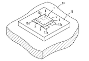
まず、本発明に係る無線ICデバイスについて図1を参照して説明する。この無線ICデバイスは、図1に示すように、所定周波数の送受信信号を処理する無線ICチップ5と、該無線ICチップ5を搭載した給電回路基板10と、誘電体である放射板20とからなる。無線ICチップ5と給電回路基板10とで電磁結合モジュール1が構成され、該電磁結合モジュール1は放射板20上に貼着されている。貼着用の接着剤は絶縁性であり、かつ、誘電体であることが好ましい。
ここで、前記電磁結合モジュール1を実装した物品について説明する。図2は電磁結合モジュール1を表面又は裏面の隅部に貼着した有価証券31を示す。図3は電磁結合モジュール1を表側又は内側に貼着したハンドバッグ32を示す。電磁結合モジュール1は有価証券31にあっては紙片自体を放射板として利用している。ハンドバッグ32にあっては、電磁結合モジュール1はハンドバッグを構成する樹脂シート上に貼着されたり、所定の誘電体シート上に貼着されて該誘電体シートがハンドバッグ32の表側あるいは内側に貼着される。
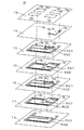
給電回路基板10に内蔵された整合回路の一例を図5に示す。この給電回路基板10は、誘電体からなるセラミックシート11A〜11Gを積層、圧着、焼成したもので、シート11Aには接続用電極12a,12b,12c,12dとビアホール導体13a,13bが形成され、シート11Bには電極14とビアホール導体13a,13b,13cが形成されている。シート11C〜11Fには線状電極15,16とビアホール導体13b,13d,13eが形成されている。さらに、シート11Gには線状電極15,16が形成されており、シート11G上において線状電極15,16は接続部17で接続されている。
なお、本発明に係る無線ICデバイスは前記実施例に限定するものではなく、その要旨の範囲内で種々に変更することができる。
5…無線ICチップ
6…入出力端子電極
10…給電回路基板
15,16…線状電極
20…放射板
26…保護膜
L1,L2…インダクタンス素子
Claims (9)
- 送受信信号を処理する無線ICチップと、
インダクタンス素子を含み、該インダクタンス素子が前記無線ICチップと電気的に導通状態で接続されている給電回路基板と、
前記無線ICチップを前記給電回路基板上に搭載した電磁結合モジュールが配置された誘電体と、
を備え、
前記電磁結合モジュールは前記誘電体に実装されており、
前記誘電体は前記電磁結合モジュールの実装部分の厚みが使用周波数に相当する波長の1/16以下であって、近距離通信用の放射板として機能すること、
を特徴とする無線ICデバイス。 - 前記給電回路基板に共振回路を備えていることを特徴とする請求項1に記載の無線ICデバイス。
- 前記給電回路基板に整合回路を備えていることを特徴とする請求項1又は請求項2に記載の無線ICデバイス。
- 前記インダクタンス素子を複数備え、
前記複数のインダクタンス素子は2本の線状電極からなり、各線状電極の一端は前記無線ICチップの入出力端子電極に電気的に接続され、他端は互いに電気的に接続されていること、を特徴とする請求項1ないし請求項3のいずれかに記載の無線ICデバイス。 - 前記2本の線状電極は互いに隣接するように配置されていることを特徴とする請求項4に記載の無線ICデバイス。
- 前記2本の線状電極はそれぞれ線路長が異なっていることを特徴とする請求項4又は請求項5に記載の無線ICデバイス。
- 前記2本の線状電極は2重の螺旋形状に配置されていることを特徴とする請求項4ないし請求項6のいずれかに記載の無線ICデバイス。
- 前記給電回路基板は多層基板で構成されていることを特徴とする請求項1ないし請求項7のいずれかに記載の無線ICデバイス。
- 前記無線ICチップ及び前記給電回路基板の少なくともいずれかを覆う保護膜が設けられていることを特徴とする請求項1ないし請求項8のいずれかに記載の無線ICデバイス。
Priority Applications (1)
| Application Number | Priority Date | Filing Date | Title |
|---|---|---|---|
| JP2007187061A JP4930236B2 (ja) | 2007-07-18 | 2007-07-18 | 無線icデバイス |
Applications Claiming Priority (1)
| Application Number | Priority Date | Filing Date | Title |
|---|---|---|---|
| JP2007187061A JP4930236B2 (ja) | 2007-07-18 | 2007-07-18 | 無線icデバイス |
Publications (3)
| Publication Number | Publication Date |
|---|---|
| JP2009027342A JP2009027342A (ja) | 2009-02-05 |
| JP2009027342A5 JP2009027342A5 (ja) | 2010-05-20 |
| JP4930236B2 true JP4930236B2 (ja) | 2012-05-16 |
Family
ID=40398754
Family Applications (1)
| Application Number | Title | Priority Date | Filing Date |
|---|---|---|---|
| JP2007187061A Active JP4930236B2 (ja) | 2007-07-18 | 2007-07-18 | 無線icデバイス |
Country Status (1)
| Country | Link |
|---|---|
| JP (1) | JP4930236B2 (ja) |
Families Citing this family (3)
| Publication number | Priority date | Publication date | Assignee | Title |
|---|---|---|---|---|
| JP5510450B2 (ja) * | 2009-04-14 | 2014-06-04 | 株式会社村田製作所 | 無線icデバイス |
| JP2011055258A (ja) * | 2009-09-02 | 2011-03-17 | Murata Mfg Co Ltd | アンテナ装置 |
| CN116902454B (zh) * | 2023-07-25 | 2024-03-15 | 国网江苏省电力有限公司泰州供电分公司 | 一种适用于多种电力物资的仓库物流容器共享系统 |
Family Cites Families (6)
| Publication number | Priority date | Publication date | Assignee | Title |
|---|---|---|---|---|
| JP4349597B2 (ja) * | 1999-03-26 | 2009-10-21 | 大日本印刷株式会社 | Icチップの製造方法及びそれを内蔵したメモリー媒体の製造方法 |
| JP4624536B2 (ja) * | 2000-04-04 | 2011-02-02 | 大日本印刷株式会社 | 非接触式データキャリア装置 |
| JP4302859B2 (ja) * | 2000-08-04 | 2009-07-29 | 日立化成工業株式会社 | 非接触式icタグ |
| JP4209230B2 (ja) * | 2003-03-24 | 2009-01-14 | トッパン・フォームズ株式会社 | 共振タグおよび非接触型データ受送信体 |
| JP4541246B2 (ja) * | 2004-12-24 | 2010-09-08 | トッパン・フォームズ株式会社 | 非接触icモジュール |
| JP4826195B2 (ja) * | 2005-09-30 | 2011-11-30 | 大日本印刷株式会社 | Rfidタグ |
-
2007
- 2007-07-18 JP JP2007187061A patent/JP4930236B2/ja active Active
Also Published As
| Publication number | Publication date |
|---|---|
| JP2009027342A (ja) | 2009-02-05 |
Similar Documents
| Publication | Publication Date | Title |
|---|---|---|
| JP5024372B2 (ja) | 無線icデバイス | |
| US8081125B2 (en) | Antenna and radio IC device | |
| US7518558B2 (en) | Wireless IC device | |
| CN102084543B (zh) | 无线ic器件 | |
| JP5482824B2 (ja) | 無線icデバイス | |
| JP4666102B2 (ja) | 無線icデバイス | |
| US7830311B2 (en) | Wireless IC device and electronic device | |
| US8360325B2 (en) | Wireless IC device, electronic apparatus, and method for adjusting resonant frequency of wireless IC device | |
| JP5370616B2 (ja) | 無線通信デバイス | |
| WO2007083574A1 (ja) | 無線icデバイス及び無線icデバイス用部品 | |
| JP4888494B2 (ja) | 電磁結合モジュール付き包装材 | |
| WO2009145218A1 (ja) | 無線icデバイス用部品および無線icデバイス | |
| CN101351924A (zh) | 无线ic器件以及无线ic器件用零件 | |
| JP4605318B2 (ja) | アンテナ及び無線icデバイス | |
| JPWO2008136220A1 (ja) | 無線icデバイス | |
| JP4930236B2 (ja) | 無線icデバイス | |
| JP5076851B2 (ja) | 無線icデバイス | |
| JPWO2008090943A1 (ja) | 電磁結合モジュール付き容器 | |
| US8720789B2 (en) | Wireless IC device | |
| JP4840275B2 (ja) | 無線icデバイス及び電子機器 | |
| JP5896594B2 (ja) | 無線icデバイス | |
| JP4867831B2 (ja) | 無線icデバイス | |
| JP5162988B2 (ja) | 無線icデバイス及びその製造方法 | |
| JP6137347B2 (ja) | 無線icデバイス及び無線icデバイス付き金属体 | |
| JP5098478B2 (ja) | 無線icデバイス及びその製造方法 |
Legal Events
| Date | Code | Title | Description |
|---|---|---|---|
| A621 | Written request for application examination |
Free format text: JAPANESE INTERMEDIATE CODE: A621 Effective date: 20100316 |
|
| A521 | Written amendment |
Free format text: JAPANESE INTERMEDIATE CODE: A523 Effective date: 20100405 |
|
| A977 | Report on retrieval |
Free format text: JAPANESE INTERMEDIATE CODE: A971007 Effective date: 20110707 |
|
| A131 | Notification of reasons for refusal |
Free format text: JAPANESE INTERMEDIATE CODE: A131 Effective date: 20110719 |
|
| A521 | Written amendment |
Free format text: JAPANESE INTERMEDIATE CODE: A523 Effective date: 20110912 |
|
| TRDD | Decision of grant or rejection written | ||
| A01 | Written decision to grant a patent or to grant a registration (utility model) |
Free format text: JAPANESE INTERMEDIATE CODE: A01 Effective date: 20120117 |
|
| A01 | Written decision to grant a patent or to grant a registration (utility model) |
Free format text: JAPANESE INTERMEDIATE CODE: A01 |
|
| A61 | First payment of annual fees (during grant procedure) |
Free format text: JAPANESE INTERMEDIATE CODE: A61 Effective date: 20120130 |
|
| R150 | Certificate of patent or registration of utility model |
Ref document number: 4930236 Country of ref document: JP Free format text: JAPANESE INTERMEDIATE CODE: R150 Free format text: JAPANESE INTERMEDIATE CODE: R150 |
|
| FPAY | Renewal fee payment (event date is renewal date of database) |
Free format text: PAYMENT UNTIL: 20150224 Year of fee payment: 3 |