JP4928811B2 - Nitride-based semiconductor light-emitting device manufacturing method and nitride-based semiconductor light-emitting device - Google Patents
Nitride-based semiconductor light-emitting device manufacturing method and nitride-based semiconductor light-emitting device Download PDFInfo
- Publication number
- JP4928811B2 JP4928811B2 JP2006078726A JP2006078726A JP4928811B2 JP 4928811 B2 JP4928811 B2 JP 4928811B2 JP 2006078726 A JP2006078726 A JP 2006078726A JP 2006078726 A JP2006078726 A JP 2006078726A JP 4928811 B2 JP4928811 B2 JP 4928811B2
- Authority
- JP
- Japan
- Prior art keywords
- nitride
- based semiconductor
- layer
- groove
- region
- Prior art date
- Legal status (The legal status is an assumption and is not a legal conclusion. Google has not performed a legal analysis and makes no representation as to the accuracy of the status listed.)
- Expired - Fee Related
Links
Images


Landscapes
- Semiconductor Lasers (AREA)
Description
本発明は、窒化物系半導体発光素子の製造方法および窒化物系半導体発光素子に関し、特に、窒化物系半導体基板上に窒化物系半導体層が形成された窒化物系半導体発光素子の製造方法および窒化物系半導体発光素子に関する。 The present invention relates to a method for manufacturing a nitride-based semiconductor light-emitting device and a nitride-based semiconductor light-emitting device, and in particular, a method for manufacturing a nitride-based semiconductor light-emitting device in which a nitride-based semiconductor layer is formed on a nitride-based semiconductor substrate, and The present invention relates to a nitride semiconductor light emitting device.
従来、窒化物系半導体基板としてのGaN基板上に、窒化物系半導体層が形成された窒化物系半導体レーザ素子などの窒化物系半導体発光素子が知られている(たとえば、特許文献1参照)。 Conventionally, nitride-based semiconductor light emitting devices such as nitride-based semiconductor laser devices in which a nitride-based semiconductor layer is formed on a GaN substrate as a nitride-based semiconductor substrate are known (see, for example, Patent Document 1). .
上記特許文献1には、平坦な表面を有するn型GaN基板上に、n型窒化物系半導体層、発光層およびp型窒化物系半導体層が順次成長されることによって形成された窒化物系半導体レーザ素子が開示されている。上記特許文献1に開示された従来の窒化物系半導体レーザ素子において、n型GaN基板上に形成されるn型窒化物系半導体層としてのn型クラッド層は、n型AlGaN層とアンドープGaN層とが交互に100層積層された構造を有する。
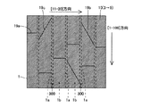
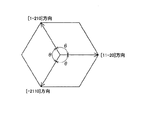
しかしながら、上記特許文献1に開示された従来の窒化物系半導体レーザ素子では、平坦な表面を有するn型GaN基板上にn型クラッド層を構成するn型AlGaN層を成長させる際に、n型AlGaN層に発生するクラックの量が増大するという不都合がある。具体的には、図24に示すように、平坦な表面を有するn型GaN基板101上にn型AlGaN層102を成長させた場合には、n型GaN基板101とn型AlGaN層102との間の格子定数差に起因してn型AlGaN層102に歪みが生じたときに、その歪みを緩和するのが困難になる。このため、平坦な表面を有するn型GaN基板101上にn型AlGaN層102を成長させた場合には、図25に示すように、n型AlGaN層102に、[11−20]方向(図26参照)と、[11−20]方向と等価な[1−210]方向および[−2110]方向(図26参照)とに延びるように発生するクラック103の量が増加する。なお、図26中のθは、120°である。
However, in the conventional nitride-based semiconductor laser device disclosed in
そして、上記特許文献1において、n型AlGaN層(n型窒化物系半導体層)に発生するクラックの量が増大する場合には、n型窒化物系半導体層上に順次形成される発光層およびp型窒化物系半導体層にも多数のクラックが発生するという不都合が生じる。これにより、上記特許文献1では、n型窒化物系半導体層、発光層およびp型窒化物系半導体層を含む窒化物系半導体素子層に多数のクラックが発生することに起因して、クラックにより窒化物系半導体素子層の発光部分に供給されないリーク電流が増大するとともに、クラックにより光導波が妨げられるという不都合がある。その結果、上記特許文献1では、窒化物系半導体レーザ素子の特性および歩留りが低下するという問題点がある。
And in the said
この発明は、上記のような課題を解決するためになされたものであり、この発明の1つの目的は、特性および歩留りの低下を抑制することが可能な窒化物系半導体発光素子の製造方法を提供することである。 The present invention has been made to solve the above-described problems, and one object of the present invention is to provide a method for manufacturing a nitride-based semiconductor light-emitting element capable of suppressing deterioration in characteristics and yield. Is to provide.
この発明のもう1つの目的は、特性および歩留りの低下を抑制することが可能な窒化物系半導体発光素子を提供することである。 Another object of the present invention is to provide a nitride-based semiconductor light-emitting device capable of suppressing deterioration in characteristics and yield.
上記目的を達成するために、この発明の1の局面による窒化物系半導体発光素子の製造方法は、窒化物系半導体基板上に形成される窒化物系半導体層の発光部分に対応する窒化物系半導体基板の第1領域以外の第2領域の所定領域を所定の深さまで選択的に除去することにより、窒化物系半導体基板に溝部を形成する工程と、窒化物系半導体基板の第1領域および溝部上に、窒化物系半導体基板とは異なる組成を有する窒化物系半導体層を形成する工程とを備えている。 In order to achieve the above object, a method for manufacturing a nitride semiconductor light emitting device according to one aspect of the present invention provides a nitride system corresponding to a light emitting portion of a nitride semiconductor layer formed on a nitride semiconductor substrate. A step of selectively removing a predetermined region of the second region other than the first region of the semiconductor substrate to a predetermined depth to form a groove in the nitride-based semiconductor substrate; a first region of the nitride-based semiconductor substrate; Forming a nitride-based semiconductor layer having a composition different from that of the nitride-based semiconductor substrate over the groove.
この局面による窒化物系半導体発光素子の製造方法では、上記のように、発光部分に対応する窒化物系半導体基板の第1領域以外の第2領域の所定領域を所定の深さまで選択的に除去することにより、窒化物系半導体基板に溝部を形成することによって、溝部の側面が窒化物系半導体基板の表面に対して垂直な場合、および、溝部の開口幅が溝部の底面から開口端に向かって徐々に小さくなっている場合には、MOCVD(Metalorganic Chemical Vapor Deposition)法などを用いて窒化物系半導体基板上に窒化物系半導体層を形成する際に、窒化物系半導体層の構成材料が溝部の側面上に堆積されにくくなるので、溝部の側面上に形成される窒化物系半導体層の厚みを、第1領域上に形成される窒化物系半導体層の厚みよりも小さくすることができる。この場合、窒化物系半導体基板と窒化物系半導体層との間の格子定数差に起因して窒化物系半導体層に歪みが生じたとしても、その歪みが溝部の側面上に位置する窒化物形半導体層の厚みが小さい部分に集中するので、第1領域での窒化物系半導体層に生じる歪みを小さくすることができる。 In the nitride-based semiconductor light-emitting device manufacturing method according to this aspect, as described above, the predetermined region of the second region other than the first region of the nitride-based semiconductor substrate corresponding to the light-emitting portion is selectively removed to a predetermined depth. Thus, by forming the groove in the nitride-based semiconductor substrate, when the side surface of the groove is perpendicular to the surface of the nitride-based semiconductor substrate, and the opening width of the groove extends from the bottom of the groove toward the opening end. If the nitride-based semiconductor layer is formed on the nitride-based semiconductor substrate using MOCVD (Metalorganic Chemical Vapor Deposition) or the like, the constituent material of the nitride-based semiconductor layer is reduced. Since it becomes difficult to deposit on the side surface of the groove portion, the thickness of the nitride-based semiconductor layer formed on the side surface of the groove portion is set to the nitridation formed on the first region. It can be made smaller than the thickness of the system semiconductor layer. In this case, even if the nitride semiconductor layer is distorted due to a lattice constant difference between the nitride semiconductor substrate and the nitride semiconductor layer, the nitride is located on the side surface of the groove. Since the concentrated semiconductor layer concentrates on the portion where the thickness is small, the strain generated in the nitride-based semiconductor layer in the first region can be reduced.
また、窒化物系半導体基板がGaN基板であり、窒化物系半導体層がAlGaN層であるとともに、溝部の開口幅が溝部の底面から開口端に向かって徐々に大きくなっている場合には、溝部の側面上に形成される窒化物系半導体層のAl組成比を、第1領域上に形成される窒化物系半導体層のAl組成比よりも低くすることができる。この理由は、MOCVD法などを用いて窒化物系半導体基板上に窒化物系半導体層を形成する際に、窒化物系半導体層の構成材料の一部であるGaがAlに比べて成膜表面を移動しやすいことにより、Gaが溝部の側面側へ移動しやすくなるためであると考えられる。このため、溝部の側面上に位置する窒化物系半導体層(AlGaN層)のAl組成比が低い部分の格子定数が窒化物系半導体基板(GaN基板)の格子定数に近づくので、溝部の側面上に位置する窒化物系半導体層のAl組成比が低い部分において、窒化物系半導体基板と窒化物系半導体層との間の格子定数差を小さくすることができる。この場合、窒化物系半導体基板と窒化物系半導体層との間の格子定数差に起因して窒化物系半導体層に歪みが生じたとしても、その歪みが溝部の側面上に位置する窒化物系半導体層のAl組成比が低い部分において緩和されるので、第1領域での窒化物系半導体層に生じる歪みを小さくすることができる。 Further, when the nitride-based semiconductor substrate is a GaN substrate, the nitride-based semiconductor layer is an AlGaN layer, and the opening width of the groove portion gradually increases from the bottom surface of the groove portion toward the opening end, the groove portion The Al composition ratio of the nitride-based semiconductor layer formed on the side surface can be made lower than the Al composition ratio of the nitride-based semiconductor layer formed on the first region. The reason for this is that when a nitride-based semiconductor layer is formed on a nitride-based semiconductor substrate using MOCVD or the like, Ga, which is a part of the constituent material of the nitride-based semiconductor layer, is deposited on the surface compared to Al. This is considered to be because Ga easily moves to the side surface side of the groove portion. For this reason, the lattice constant of the portion with a low Al composition ratio of the nitride-based semiconductor layer (AlGaN layer) located on the side surface of the groove portion approaches the lattice constant of the nitride-based semiconductor substrate (GaN substrate). The difference in lattice constant between the nitride-based semiconductor substrate and the nitride-based semiconductor layer can be reduced in the portion where the Al composition ratio of the nitride-based semiconductor layer located at is low. In this case, even if the nitride semiconductor layer is distorted due to a lattice constant difference between the nitride semiconductor substrate and the nitride semiconductor layer, the nitride is located on the side surface of the groove. Since the Al composition ratio of the system semiconductor layer is relaxed at the low portion, the strain generated in the nitride semiconductor layer in the first region can be reduced.
このように、この局面では、窒化物系半導体層に生じる歪みを小さくすることができるので、窒化物系半導体層に生じる歪みが大きいことに起因して、窒化物系半導体層に発生するクラックの量が増大するという不都合が発生するのを抑制することができる。したがって、クラックにより窒化物系半導体層の発光部分に供給されないリーク電流が増大するとともに、クラックにより光導波が妨げられるという不都合が発生するのを抑制することができる。その結果、窒化物系半導体発光素子の特性および歩留りの低下を抑制することができる。 Thus, in this aspect, since the strain generated in the nitride-based semiconductor layer can be reduced, cracks generated in the nitride-based semiconductor layer due to the large strain generated in the nitride-based semiconductor layer. Generation | occurrence | production of the problem that the quantity increases can be suppressed. Accordingly, it is possible to suppress the occurrence of the disadvantage that the leakage current that is not supplied to the light emitting portion of the nitride-based semiconductor layer due to the crack increases and that the optical waveguide is hindered by the crack. As a result, it is possible to suppress a decrease in characteristics and yield of the nitride semiconductor light emitting device.
上記局面による窒化物系半導体発光素子の製造方法において、好ましくは、窒化物系半導体基板は、GaN基板を含み、窒化物系半導体層は、AlとGaとNとを含有する層を含む。このように構成すれば、GaN基板と、GaN基板上に形成されたAlGaN層(AlとGaとNとを含有する層)を含む窒化物系半導体層とを備えた窒化物系半導体発光素子において、GaN基板とAlGaN層との間の格子定数差に起因して、窒化物系半導体層に発生するクラックの量が増大するという不都合が発生するのを容易に抑制することができる。 In the method for manufacturing a nitride semiconductor light emitting device according to the above aspect, preferably, the nitride semiconductor substrate includes a GaN substrate, and the nitride semiconductor layer includes a layer containing Al, Ga, and N. With this configuration, in a nitride-based semiconductor light-emitting device including a GaN substrate and a nitride-based semiconductor layer including an AlGaN layer (a layer containing Al, Ga, and N) formed on the GaN substrate. It is possible to easily suppress the occurrence of the disadvantage that the amount of cracks generated in the nitride-based semiconductor layer increases due to the lattice constant difference between the GaN substrate and the AlGaN layer.
上記窒化物系半導体基板がGaN基板を含むとともに、窒化物系半導体層がAlとGaとNとを含有する層を含む構成において、好ましくは、窒化物系半導体基板上に窒化物系半導体層を形成する工程は、窒化物系半導体基板の第1領域の上面上、溝部の底面および側面上に窒化物系半導体層を形成する工程を含み、溝部の側面上に形成される窒化物系半導体層のAl組成比は、第1領域の上面上に形成される窒化物系半導体層のAl組成比よりも低い。このように構成すれば、溝部の側面上に位置する窒化物系半導体層(AlGaN層)のAl組成比が低い部分の格子定数が窒化物系半導体基板(GaN基板)の格子定数に近づくので、溝部の側面上に位置する窒化物系半導体層のAl組成比が低い部分において、窒化物系半導体基板と窒化物系半導体層との間の格子定数差を小さくすることができる。これにより、窒化物系半導体基板と窒化物系半導体層との間の格子定数差に起因して窒化物系半導体層に歪みが生じたとしても、容易に、溝部の側面上に位置する窒化物系半導体層のAl組成比が低い部分において歪みを緩和することができる。 In the configuration in which the nitride-based semiconductor substrate includes a GaN substrate and the nitride-based semiconductor layer includes a layer containing Al, Ga, and N, preferably, the nitride-based semiconductor layer is provided on the nitride-based semiconductor substrate. The step of forming includes a step of forming a nitride-based semiconductor layer on the top surface of the first region of the nitride-based semiconductor substrate, the bottom surface and the side surface of the groove portion, and the nitride-based semiconductor layer formed on the side surface of the groove portion The Al composition ratio is lower than the Al composition ratio of the nitride-based semiconductor layer formed on the upper surface of the first region. If configured in this way, the lattice constant of the portion with a low Al composition ratio of the nitride-based semiconductor layer (AlGaN layer) located on the side surface of the groove portion approaches the lattice constant of the nitride-based semiconductor substrate (GaN substrate), The lattice constant difference between the nitride-based semiconductor substrate and the nitride-based semiconductor layer can be reduced in the portion where the Al composition ratio of the nitride-based semiconductor layer located on the side surface of the groove is low. As a result, even if the nitride-based semiconductor layer is distorted due to the lattice constant difference between the nitride-based semiconductor substrate and the nitride-based semiconductor layer, the nitride located on the side surface of the groove is easily The strain can be relaxed in the portion where the Al composition ratio of the semiconductor layer is low.
この場合、好ましくは、窒化物系半導体基板に溝部を形成する工程は、溝部の開口幅が、溝部の底面から開口端に向かって徐々に大きくなるように形成する工程を含む。このように構成すれば、MOCVD法などを用いて窒化物系半導体基板上に窒化物系半導体層を形成する際に、窒化物系半導体層の構成材料の一部であるGaがAlに比べて成膜表面を移動しやすいことにより、Gaが溝部の側面側へ移動しやすくなると考えられるので、容易に、溝部の側面上に形成される窒化物系半導体層のAl組成比を、第1領域上に形成される窒化物系半導体層のAl組成比よりも低くすることができる。 In this case, preferably, the step of forming the groove portion in the nitride-based semiconductor substrate includes a step of forming the groove portion so that the opening width of the groove portion gradually increases from the bottom surface of the groove portion toward the opening end. With this configuration, when a nitride semiconductor layer is formed on a nitride semiconductor substrate using MOCVD or the like, Ga, which is a part of the material constituting the nitride semiconductor layer, is larger than Al. Since it is considered that Ga easily moves to the side surface side of the groove portion due to easy movement of the film formation surface, the Al composition ratio of the nitride-based semiconductor layer formed on the side surface of the groove portion can be easily set to the first region. It can be made lower than the Al composition ratio of the nitride-based semiconductor layer formed thereon.
上記局面による窒化物系半導体発光素子の製造方法において、好ましくは、窒化物系半導体基板上に窒化物系半導体層を形成する工程は、窒化物系半導体基板の第1領域の上面上、溝部の底面および側面上に窒化物系半導体層を形成する工程を含み、溝部の側面上に形成される窒化物系半導体層の厚みは、第1領域の上面上に形成される窒化物系半導体層の厚みよりも小さい。このように構成すれば、窒化物系半導体基板と窒化物系半導体層との間の格子定数差に起因して窒化物系半導体層に歪みが生じたとしても、溝部の側面上に位置する窒化物形半導体層の厚みが小さい部分に歪みが集中するので、容易に、第1領域での窒化物系半導体層の歪みを緩和することができる。 In the method for manufacturing a nitride-based semiconductor light-emitting device according to the above aspect, preferably, the step of forming the nitride-based semiconductor layer on the nitride-based semiconductor substrate includes the step of forming a groove on the upper surface of the first region of the nitride-based semiconductor substrate. Including a step of forming a nitride-based semiconductor layer on the bottom surface and the side surface, and the thickness of the nitride-based semiconductor layer formed on the side surface of the groove is the same as that of the nitride-based semiconductor layer formed on the upper surface of the first region Less than thickness. With this configuration, even if distortion occurs in the nitride-based semiconductor layer due to the difference in lattice constant between the nitride-based semiconductor substrate and the nitride-based semiconductor layer, the nitride located on the side surface of the groove portion Since strain concentrates on the portion where the thickness of the physical semiconductor layer is small, the strain of the nitride-based semiconductor layer in the first region can be easily relaxed.
上記溝部の側面上に形成される窒化物系半導体層の厚みが第1領域の上面上に形成される窒化物系半導体層の厚みよりも小さい場合において、窒化物系半導体基板に溝部を形成する工程は、溝部の側面が、窒化物系半導体基板の表面に対して実質的に垂直になるように形成する工程を含んでいてもよい。このように構成すれば、MOCVD法などを用いて窒化物系半導体基板上に窒化物系半導体層を形成する際に、窒化物系半導体層の構成材料が溝部の側面上に堆積されにくくなるので、容易に、溝部の側面上に形成される窒化物系半導体層の厚みを、第1領域上に形成される窒化物系半導体層の厚みよりも小さくすることができる。 When the thickness of the nitride-based semiconductor layer formed on the side surface of the groove is smaller than the thickness of the nitride-based semiconductor layer formed on the upper surface of the first region, the groove is formed in the nitride-based semiconductor substrate. The step may include a step of forming the side surface of the groove portion so as to be substantially perpendicular to the surface of the nitride-based semiconductor substrate. With this configuration, when the nitride-based semiconductor layer is formed on the nitride-based semiconductor substrate using the MOCVD method or the like, it is difficult for the constituent material of the nitride-based semiconductor layer to be deposited on the side surface of the groove. The thickness of the nitride-based semiconductor layer formed on the side surface of the groove can be easily made smaller than the thickness of the nitride-based semiconductor layer formed on the first region.
上記溝部の側面上に形成される窒化物系半導体層の厚みが第1領域の上面上に形成される窒化物系半導体層の厚みよりも小さい場合において、窒化物系半導体基板に溝部を形成する工程は、溝部の開口幅が、溝部の底面から開口端に向かって徐々に小さくなるように形成する工程を含んでいてもよい。このように構成すれば、MOCVD法などを用いて窒化物系半導体基板上に窒化物系半導体層を形成する際に、溝部の側面が窒化物系半導体基板の表面に対して実質的に垂直である場合に比べて、窒化物系半導体層の構成材料が溝部の側面上に堆積されにくくなるので、より容易に、溝部の側面上に形成される窒化物系半導体層の厚みを、第1領域上に形成される窒化物系半導体層の厚みよりも小さくすることができる。 When the thickness of the nitride-based semiconductor layer formed on the side surface of the groove is smaller than the thickness of the nitride-based semiconductor layer formed on the upper surface of the first region, the groove is formed in the nitride-based semiconductor substrate. The step may include a step of forming the groove portion so that the opening width of the groove portion gradually decreases from the bottom surface of the groove portion toward the opening end. With this configuration, when the nitride-based semiconductor layer is formed on the nitride-based semiconductor substrate using the MOCVD method or the like, the side surface of the groove is substantially perpendicular to the surface of the nitride-based semiconductor substrate. Since the constituent material of the nitride-based semiconductor layer is less likely to be deposited on the side surface of the groove portion than in some cases, the thickness of the nitride-based semiconductor layer formed on the side surface of the groove portion can be more easily set to the first region. It can be made smaller than the thickness of the nitride-based semiconductor layer formed thereon.
上記局面による窒化物系半導体発光素子の製造方法において、窒化物系半導体基板に溝部を形成する工程は、窒化物系半導体基板に、所定の方向に延びる細長状の溝部を形成する工程を含んでいてもよい。このように構成すれば、所定の方向と交差する方向に延びるように発生するクラックが、所定の方向に延びる溝部に対応する領域を横切って伝播するのを抑制することができる。 In the method for manufacturing a nitride semiconductor light emitting device according to the above aspect, the step of forming the groove portion in the nitride semiconductor substrate includes the step of forming an elongated groove portion extending in a predetermined direction in the nitride semiconductor substrate. May be. If comprised in this way, it can suppress that the crack generated so that it may extend in the direction which cross | intersects a predetermined direction propagates across the area | region corresponding to the groove part extended in a predetermined direction.
窒化物系半導体基板の表面が(H,K,−H−K,0)面を有する場合には、
溝部を[K,−H,−H+K,0]方向に沿って延びるように形成するのが好ましい(HとKは整数であり、HとKの少なくとも一方は0ではない)。このように構成すれば、クラックが発生し易い[0001]方向と交差する方向へのクラックの伝搬を効果的に抑制できる。
When the surface of the nitride-based semiconductor substrate has a (H, K, -HK, 0) plane,
The groove is preferably formed so as to extend along the [K, -H, -H + K, 0] direction (H and K are integers, and at least one of H and K is not 0). If comprised in this way, the propagation of the crack to the direction which crosses the [0001] direction where a crack is easy to generate | occur | produce can be suppressed effectively.
上記局面による窒化物系半導体発光素子の製造方法において、窒化物系半導体基板に溝部を形成する工程は、窒化物系半導体基板に、第1領域を囲むように、第1の方向および第1の方向と交差する第2の方向に延びる細長状の溝部を格子状に形成する工程を含んでいてもよい。このように構成すれば、第1の方向と交差する方向に延びるように発生するクラックが、少なくとも第1の方向に延びる溝部に対応する領域を横切って伝播するのを抑制することができるとともに、第2の方向と交差する方向に延びるように発生するクラックが、少なくとも第2の方向に延びる溝部に対応する領域を横切って伝播するのを抑制することができる。これにより、第1の方向および第2の方向の両方に延びるように発生するクラックを溝部で分断することができるので、クラックの量が増大するのをより有効に抑制することができる。 In the method for manufacturing a nitride-based semiconductor light-emitting device according to the above aspect, the step of forming the groove portion in the nitride-based semiconductor substrate includes the first direction and the first direction so as to surround the first region in the nitride-based semiconductor substrate. A step of forming elongated grooves extending in a second direction intersecting the direction in a lattice shape may be included. If constituted in this way, while being able to suppress that a crack generated so as to extend in a direction intersecting the first direction propagates at least across a region corresponding to the groove extending in the first direction, A crack generated so as to extend in a direction intersecting the second direction can be suppressed from propagating across at least a region corresponding to the groove extending in the second direction. Thereby, since the crack which generate | occur | produces so that it may extend in both the 1st direction and the 2nd direction can be parted by a groove part, it can suppress more effectively that the quantity of a crack increases.
この発明の別の局面による窒化物系半導体発光素子は、発光部分に対応する第1領域と、所定の高さを有する段差部を介して第1領域に隣接するように配置された第2領域とを含む窒化物系半導体基板と、窒化物系半導体基板の第1領域の上面および段差部の側面上に形成されるとともに、窒化物系半導体基板とは異なる組成を有する窒化物系半導体層とを備えている。そして、段差部の側面上に形成される窒化物系半導体層の厚みは、第1領域の上面上に形成される窒化物系半導体層の厚みよりも小さい。 A nitride-based semiconductor light-emitting device according to another aspect of the present invention includes a first region corresponding to a light-emitting portion and a second region disposed adjacent to the first region via a stepped portion having a predetermined height. And a nitride semiconductor layer formed on the upper surface of the first region and the side surface of the step portion of the nitride semiconductor substrate and having a composition different from that of the nitride semiconductor substrate, It has. The thickness of the nitride-based semiconductor layer formed on the side surface of the step portion is smaller than the thickness of the nitride-based semiconductor layer formed on the upper surface of the first region.
この局面による窒化物系半導体発光素子では、上記のように、窒化物系半導体基板の段差部の側面上に形成される窒化物系半導体層の厚みを、発光部分に対応する窒化物系半導体基板の第1領域の上面上に形成される窒化物系半導体層の厚みよりも小さくすることによって、MOCVD法などを用いて窒化物系半導体基板上に窒化物系半導体層を形成する際に、窒化物系半導体基板と窒化物系半導体層との間の格子定数差に起因して窒化物系半導体層に歪みが生じたとしても、段差部の側面上に位置する窒化物形半導体層の厚みが小さい部分に歪みが集中するので、第1領域での窒化物系半導体層に生じる歪みを小さくすることができる。これにより、窒化物系半導体層に生じる歪みが大きいことに起因して、窒化物系半導体層に発生するクラックの量が増大するという不都合が発生するのを抑制することができる。したがって、クラックにより窒化物系半導体層の発光部分に供給されないリーク電流が増大するとともに、クラックにより光導波が妨げられるという不都合が発生するのを抑制することができる。その結果、窒化物系半導体発光素子の特性および歩留りの低下を抑制することができる。 In the nitride-based semiconductor light-emitting device according to this aspect, as described above, the nitride-based semiconductor substrate corresponding to the light-emitting portion has a thickness of the nitride-based semiconductor layer formed on the side surface of the stepped portion of the nitride-based semiconductor substrate. When the nitride-based semiconductor layer is formed on the nitride-based semiconductor substrate using the MOCVD method or the like by making the thickness smaller than the thickness of the nitride-based semiconductor layer formed on the upper surface of the first region, Even if the nitride semiconductor layer is distorted due to the difference in lattice constant between the nitride semiconductor substrate and the nitride semiconductor layer, the thickness of the nitride semiconductor layer located on the side surface of the stepped portion is Since strain concentrates on a small portion, strain generated in the nitride-based semiconductor layer in the first region can be reduced. Thereby, it is possible to suppress the occurrence of the disadvantage that the amount of cracks generated in the nitride-based semiconductor layer increases due to the large strain generated in the nitride-based semiconductor layer. Accordingly, it is possible to suppress the occurrence of the disadvantage that the leakage current that is not supplied to the light emitting portion of the nitride-based semiconductor layer due to the crack increases and that the optical waveguide is hindered by the crack. As a result, it is possible to suppress a decrease in characteristics and yield of the nitride semiconductor light emitting device.
この発明のまた別の局面による窒化物系半導体発光素子は、発光部分に対応する第1領域と、所定の高さを有する段差部を介して第1領域に隣接するように配置された第2領域とを含む窒化物系半導体基板と、窒化物系半導体基板の第1領域の上面および段差部の側面上に形成されるとともに、窒化物系半導体基板とは異なる組成を有するとともに、AlとGaとNとを含有する窒化物系半導体層とを備えている。そして、段差部の側面上に形成される窒化物系半導体層のAl組成比は、第1領域の上面上に形成される窒化物系半導体層のAl組成比よりも低い。 A nitride-based semiconductor light-emitting device according to yet another aspect of the present invention includes a first region corresponding to the light-emitting portion and a second region disposed adjacent to the first region via a stepped portion having a predetermined height. A nitride-based semiconductor substrate including a region, and a nitride-based semiconductor substrate having a composition different from that of the nitride-based semiconductor substrate and Al and Ga. And a nitride-based semiconductor layer containing N. The Al composition ratio of the nitride-based semiconductor layer formed on the side surface of the step portion is lower than the Al composition ratio of the nitride-based semiconductor layer formed on the upper surface of the first region.
この局面による窒化物系半導体発光素子では、上記のように、窒化物系半導体基板の段差部の側面上に形成されるAlとGaとNとを含有する窒化物系半導体層のAl組成比を、発光部分に対応する窒化物系半導体基板の第1領域の上面上に形成される窒化物系半導体層のAl組成比よりも低くすることによって、MOCVD法などを用いて窒化物系半導体基板上に窒化物系半導体層を形成する際に、段差部の側面上に位置するAlとGaとNとを含有する窒化物系半導体層のAl組成比が低い部分の格子定数が、AlとGaとNとを含有する窒化物系半導体層とは異なる組成を有する窒化物系半導体基板の格子定数に近づくので、段差部の側面上に位置する窒化物系半導体層のAl組成比が低い部分において、窒化物系半導体基板と窒化物系半導体層との間の格子定数差を小さくすることができる。このため、窒化物系半導体基板と窒化物系半導体層との間の格子定数差に起因して窒化物系半導体層に歪みが生じたとしても、段差部の側面上に位置する窒化物系半導体層のAl組成比が低い部分において歪みを緩和することができるので、窒化物系半導体層に生じる歪みを小さくすることができる。これにより、窒化物系半導体層に生じる歪みが大きいことに起因して、窒化物系半導体層に発生するクラックの量が増大するという不都合が発生するのを抑制することができる。したがって、クラックにより窒化物系半導体層の発光部分に供給されないリーク電流が増大するとともに、クラックにより光導波が妨げられるという不都合が発生するのを抑制することができる。その結果、窒化物系半導体発光素子の特性および歩留りの低下を抑制することができる。 In the nitride semiconductor light emitting device according to this aspect, as described above, the Al composition ratio of the nitride semiconductor layer containing Al, Ga, and N formed on the side surface of the step portion of the nitride semiconductor substrate is set. By using an MOCVD method or the like on the nitride semiconductor substrate by lowering the Al composition ratio of the nitride semiconductor layer formed on the upper surface of the first region of the nitride semiconductor substrate corresponding to the light emitting portion When the nitride-based semiconductor layer is formed on the side surface of the stepped portion, the lattice constant of the portion of the nitride-based semiconductor layer containing Al, Ga, and N having a low Al composition ratio is Al, Ga, and Since it approaches the lattice constant of a nitride-based semiconductor substrate having a composition different from that of a nitride-based semiconductor layer containing N, in the portion where the Al composition ratio of the nitride-based semiconductor layer located on the side surface of the step portion is low, Nitride semiconductor substrate and nitride It is possible to reduce the lattice constant difference between the semiconductor layer. Therefore, even if the nitride semiconductor layer is distorted due to the difference in lattice constant between the nitride semiconductor substrate and the nitride semiconductor layer, the nitride semiconductor located on the side surface of the step portion Since strain can be relaxed in a portion where the Al composition ratio of the layer is low, strain generated in the nitride-based semiconductor layer can be reduced. Thereby, it is possible to suppress the occurrence of the disadvantage that the amount of cracks generated in the nitride-based semiconductor layer increases due to the large strain generated in the nitride-based semiconductor layer. Accordingly, it is possible to suppress the occurrence of the disadvantage that the leakage current that is not supplied to the light emitting portion of the nitride-based semiconductor layer due to the crack increases and that the optical waveguide is hindered by the crack. As a result, it is possible to suppress a decrease in characteristics and yield of the nitride semiconductor light emitting device.
また、この局面において、窒化物系半導体基板の表面は(H,K,−H−K,0)面を有する場合には、溝部は[K,−H,−H+K,0]方向に沿って延びるように形成されていることが好ましい(HとKは整数であり、HとKの少なくとも一方は0ではない)。このように構成すれば、クラックが発生し易い[0001]方向と交差する方向へのクラックの伝搬を効果的に抑制できる。 Further, in this aspect, when the surface of the nitride-based semiconductor substrate has a (H, K, -HK, 0) plane, the groove is along the [K, -H, -H + K, 0] direction. It is preferably formed so as to extend (H and K are integers, and at least one of H and K is not 0). If comprised in this way, the propagation of the crack to the direction which crosses the [0001] direction where a crack is easy to generate | occur | produce can be suppressed effectively.
以下、本発明の実施形態を図面に基づいて説明する。 Hereinafter, embodiments of the present invention will be described with reference to the drawings.
(第1参考形態)
図1〜図11は、本発明の第1参考形態による窒化物系半導体レーザ素子の製造プロセスを説明するための平面図および断面図である。図12は、本発明の第1参考形態による窒化物系半導体レーザ素子の製造プロセスを用いて形成された窒化物系半導体レーザ素子の構造を示した断面図である。図1〜図12および図26を参照して、以下に第1参考形態による窒化物系半導体レーザ素子の製造プロセスについて説明する。
(First reference form)
1 to 11 are a plan view and a cross-sectional view for explaining the manufacturing process of the first reference embodiment according to the nitride semiconductor laser device of the present invention. Figure 12 is a first sectional view showing a structure of a nitride-based semiconductor laser device formed by the manufacturing process for the nitride-based semiconductor laser device according to another embodiment of the present invention. Referring to FIGS. 1 to 12 and 26, will be described the manufacturing process of the first reference embodiment according to the nitride semiconductor laser device below.
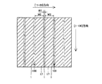
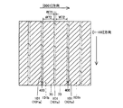
第1参考形態による窒化物系半導体レーザ素子の製造プロセスでは、図1および図2に示すように、まず、(0001)面の表面を有するとともに、低い転位密度を有するn型GaN基板1を準備する。このn型GaN基板1は、約0.3189nm(a軸方向)の格子定数を有する。なお、n型GaN基板1は、本発明の「窒化物系半導体基板」の一例である。そして、電子ビーム蒸着法などを用いて、n型GaN基板1上の所定領域に、約0.4μmの厚みを有するNi層からなるストライプ状(細長状)のマスク層17を形成する。具体的には、マスク層17が、[1−100]方向に延びるように形成する。また、[11−20]方向に隣接するマスク層17間の距離W1を、約50μmに設定するとともに、マスク層17の[11−20]方向の幅W2を、約200μmに設定する。
In the manufacturing process for the nitride-based semiconductor laser device according to the first referential embodiment, as shown in FIGS. 1 and 2, first, and has a surface of (0001) plane, prepared n-
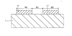
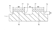
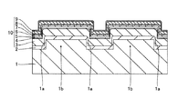
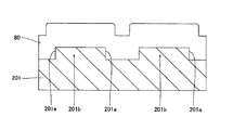
次に、図3および図4に示すように、Cl2ガスによるRIE(Reactive Ion Etching)法を用いて、マスク層17をエッチングマスクとして、n型GaN基板1の上面から約2μmの深さまでをエッチングする。なお、この場合のエッチング選択比(マスク層17/n型GaN基板1)は、1:10である。また、エッチング条件としては、エッチング圧力:約3.325kPa、プラズマパワー:約200W、エッチング速度:約140nm/sec〜約150nm/secである。これにより、n型GaN基板1に、約50μmの幅W1と、約2μmの深さD1とを有するとともに、[1−100]方向に延びるストライプ状(細長状)の溝部1aが形成される。また、上記のエッチング条件の場合、溝部1aの側面が、n型GaN基板1の上面に対して垂直となる。そして、n型GaN基板1において、溝部1aに挟まれた約200μmの[11−20]方向の幅W2を有する領域1bは、後述する窒化物系半導体素子層10の発光部分に対応する領域となる。なお、n型GaN基板1の領域1bは、本発明の「第1領域」の一例であり、n型GaN基板1の溝部1aが形成された領域は、本発明の「第2領域」の一例である。この後、マスク層17を除去する。
Next, as shown in FIGS. 3 and 4, from the upper surface of the n-
次に、図5および図6に示すように、MOCVD法を用いて、n型GaN基板1の領域1bの上面上、溝部1aの底面および側面上に、バッファ層2を介して、窒化物系半導体素子層10を構成する窒化物形半導体各層(3〜9)を順次形成する。
Next, as shown in FIGS. 5 and 6, a nitride system is formed on the top surface of the
具体的には、図6に示すように、まず、溝部1aが形成されたn型GaN基板1を、水素および窒素雰囲気の反応炉の中に挿入する。この後、窒化物系半導体各層(2〜9)の窒素原料であるNH3ガスを反応炉内に供給するとともに、基板温度が約1160℃になるまで加熱する。そして、基板温度が約1160℃付近にまで達した時点で、Ga原料であるTMGa(トリメチルガリウム)ガスおよびAl原料であるTMAl(トリメチルアルミニウム)ガスを、キャリアガスとしてのH2ガスを用いて反応炉内に供給することによって、n型GaN基板1上に、約0.8μmの厚みを有するアンドープAl0.01Ga0.99Nからなるバッファ層2を約1.1μm/hの速度で成長させる。この後、TMGaガスおよびTMAlガスと、n型不純物としてのGe原料であるGeH4(モノゲルマン)ガスとを、キャリアガスとしてのH2ガスを用いて反応炉内に供給することによって、バッファ層2上に、約1.8μmの厚みを有するGeがドープされたn型Al0.07Ga0.93Nからなるn型クラッド層3を約1.1μm/hの速度で成長させる。このn型Al0.07Ga0.93Nからなるn型クラッド層3の格子定数は、約0.3184nm(a軸方向)である。なお、n型Al0.07Ga0.93Nからなるn型クラッド層3の格子定数は、GaNの格子定数(約0.3814nm(a軸方向))と、AlNの格子定数(約0.3112nm(a軸方向))とに基づいて算出した値である。なお、n型クラッド層3は、本発明の「窒化物系半導体層」の一例である。さらに、TMGaガスおよびTMAlガスを、キャリアガスとしてのH2ガスを用いて反応炉内に供給することによって、n型クラッド層3上に、約20nmの厚みを有するアンドープAl0.2Ga0.8Nからなるn側キャリアブロック層4を約1μm/hの速度で成長させる。
Specifically, as shown in FIG. 6, first, the n-
次に、基板温度を約1160℃から約850℃に下げる。そして、Ga原料であるTEGa(トリエチルガリウム)ガスおよびIn原料であるTMIn(トリメチルインジウム)ガスを、キャリアガスとしてのN2ガスを用いて反応炉内に供給することによって、n側キャリアブロック層4上に、約20nmの厚みを有するアンドープIn0.02Ga0.93Nからなる4つの量子障壁層(図示せず)と、約3.5nmの厚みを有するアンドープIn0.15Ga0.85Nからなる3つの量子井戸層(図示せず)とを交互に約0.25μm/hの速度で成長させる。これにより、4つの量子障壁層と3つの量子井戸層とが交互に積層された多重量子井戸(MQW:Multiple Quantum Well)構造を有するMQW活性層5が形成される。続けて、MQW活性層5上に、約0.1μmの厚みを有するアンドープIn0.01Ga0.99Nからなるp側光ガイド層6を成長させる。この後、TMGaガスおよびTMAlガスを、キャリアガスとしてのN2ガスを用いて反応炉内に供給することによって、p側光ガイド層6上に、約20nmの厚みを有するアンドープAl0.2Ga0.8Nからなるp側キャリアブロック層7を約1.2μm/hの速度で成長させる。
Next, the substrate temperature is lowered from about 1160 ° C. to about 850 ° C. Then, a TEGa (triethylgallium) gas as a Ga raw material and a TMIn (trimethylindium) gas as an In raw material are supplied into the reaction furnace using N 2 gas as a carrier gas, whereby the n-side
次に、基板温度を約850℃から約1000℃に加熱する。そして、TMGaガスおよびTMAlガスと、p型不純物としてのMg原料であるMg(C5H5)2(シクロペンタジエニルマグネシウム)ガスとを、キャリアガスとしてのN2ガスを用いて反応炉内に供給することによって、p側キャリアブロック層7上に、約0.45μmの厚みを有するMgがドープされたp型Al0.07Ga0.93Nからなるp型クラッド層8を約1.1μm/hの速度で成長させる。この後、基板温度を約1000℃から約850℃に下げる。そして、TEGaガスおよびTMInガスを、キャリアガスとしてのN2ガスを用いて反応炉内に供給することによって、p型クラッド層8上に、約3nmの厚みを有するアンドープIn0.07Ga0.93Nからなるp側コンタクト層9を約0.25μm/hの速度で成長させる。これにより、n型GaN基板1の領域1bの上面上、溝部1aの底面および側面上に、バッファ層2を介して、窒化物形半導体各層(3〜9)により構成される窒化物系半導体素子層10が形成される。
Next, the substrate temperature is heated from about 850 ° C. to about 1000 ° C. Then, TMGa gas and TMAl gas, and Mg (C 5 H 5 ) 2 (cyclopentadienylmagnesium) gas, which is an Mg raw material as a p-type impurity, are used in the reactor using N 2 gas as a carrier gas. P-
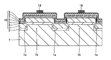
この際、第1参考形態では、[1−100]方向(図5参照)に延びる溝部1aの側面上に形成された窒化物形半導体各層(2〜9)の厚みは、それぞれ、n型GaN基板1の領域1b上に形成された窒化物系半導体各層(2〜9)の厚みよりも小さくなる。このため、約0.3189nmの格子定数を有するn型GaN基板1と、約0.3184nmの格子定数を有するn型Al0.07Ga0.93Nからなるn型クラッド層3との間の格子定数差に起因してn型クラッド層3に歪みが生じたとしても、その歪みが溝部1aの側面上に位置するn型クラッド層3の厚みが小さい部分に集中するので、n型GaN基板1の領域1b上に位置するn型クラッド層3に生じる歪みが緩和される。これにより、図5に示すように、n型クラッド層3に生じる歪みが大きいことに起因して、n型クラッド層3に発生するクラック19a〜19cの量が増大するという不都合が発生するのが抑制される。したがって、n型クラッド層3を含む窒化物系半導体素子層10に発生するクラック19a〜19cの量が増大するのも抑制される。
At this time, in the first reference embodiment, the thickness of each nitride semiconductor layer (2-9) formed on the side surface of the
また、第1参考形態では、[11−20]方向に延びるように発生するクラック19a、[1−210]方向(図26参照)に延びるように発生するクラック19bおよび[−2110]方向(図26参照)に延びるように発生するクラック19cが、[1−100]方向に延びる溝部1aに対応する領域と交差するので、クラック19a〜19cが溝部1aに対応する領域を横切って伝播するのが抑制される。
Further, in the first reference embodiment, the
この後、窒化物系半導体素子層10が形成されたn型GaN基板1を反応炉内から取り出す。
Thereafter, the n-
次に、図7に示すように、プラズマCVD法を用いて、p側コンタクト層9上のn型GaN基板1の領域1bに対応する所定領域に、SiO2膜からなるストライプ状(細長状)のマスク層18を形成する。具体的には、マスク層18が、[1−100]方向(図5参照)に延びるように形成する。また、マスク層18の[11−20]方向(図5参照)の幅を、約1.5μmに設定する。
Next, as shown in FIG. 7, in a predetermined region corresponding to the
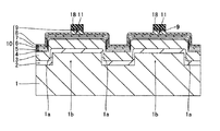
次に、図8に示すように、Cl2ガスによるRIE法を用いて、マスク層18をエッチングマスクとして、p側コンタクト層9およびp型クラッド層8の上面から約0.4μmの厚み分をエッチングする。これにより、p型クラッド層8の凸部とp側コンタクト層9とにより構成されるとともに、[1−100]方向(図5参照)に延びるストライプ状(細長状)のリッジ部11が形成される。また、リッジ部11は、約1.5μmの[11−20]方向(図5参照)の幅と、約0.402μmの突出高さとを有するように形成される。このリッジ部11は、電流通路になるとともに、このリッジ部11の下方が発光部分となる。また、p型クラッド層8の凸部以外の平坦部の厚みは、約0.05μmとなる。この後、マスク層18を除去する。
Next, as shown in FIG. 8, a thickness of about 0.4 μm is formed from the upper surfaces of the p-
次に、図9に示すように、プラズマCVD法を用いて、全面上に、約0.2μmの厚みを有するSiO2膜を形成した後、そのSiO2膜のリッジ部11に対応する領域を除去することによって、リッジ部11に対応する領域に開口部12aを有する電流ブロック層12を形成する。
Next, as shown in FIG. 9, using a plasma CVD method, on the entire surface, after forming the SiO 2 film having a thickness of about 0.2 [mu] m, an area corresponding to the
次に、図10に示すように、電子ビーム蒸着法を用いて、リッジ部11を構成するp側コンタクト層9上に、p側オーミック電極13を形成する。このp側オーミック電極13を形成する際には、下層から上層に向かって、約1nmの厚みを有するPt層と、約10nmの厚みを有するPd層とを順次形成する。この後、電子ビーム蒸着法を用いて、電流ブロック層12上に、p側オーミック電極13の上面に接触するように、p側パッド電極14を形成する。このp側パッド電極14を形成する際には、下層から上層に向かって、約30nmの厚みを有するTi層と、約150nmの厚みを有するPd層と、約3μmの厚みを有するAu層とを順次形成する。
Next, as shown in FIG. 10, the p-
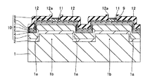
次に、図11に示すように、n型GaN基板1の裏面を、後述する劈開工程において劈開しやすい厚みになるまで研磨する。この後、電子ビーム蒸着法を用いて、n型GaN基板1の裏面上の所定領域に、n側オーミック電極15と、約300nmの厚みを有するAu層からなるn側パッド電極16とを順次形成する。なお、n側オーミック電極15を形成する際には、n型GaN基板1の裏面側から順に、約6nmの厚みを有するAl層と、約10nmの厚みを有するPd層とを形成する。
Next, as shown in FIG. 11, the back surface of the n-
最後に、図11に示した構造体において、[1−100]方向(図5参照)にn型GaN基板1の溝部1aの中心に沿って素子分離するとともに、[11−20]方向(図5参照)に素子を各チップに劈開することによって、図12に示すような第1参考形態による窒化物系半導体レーザ素子が形成される。
Finally, in the structure shown in FIG. 11, the element is separated along the center of the
なお、図12に示すように、第1参考形態の製造プロセスにより形成された窒化物系半導体レーザ素子において、n型GaN基板1の溝部1a(図11参照)は、上記した素子分離工程により垂直な側面を有する段差部1cとなる。すなわち、第1参考形態の製造プロセスにより形成された窒化物系半導体レーザ素子では、n型GaN基板1の段差部1cの側面上に形成された窒化物形半導体各層(2〜9)の厚みが、それぞれ、n型GaN基板1の領域1b上に形成された窒化物系半導体各層(2〜9)の厚みよりも小さくなる。
As shown in FIG. 12, in the nitride-based semiconductor laser device formed by the manufacturing process of the first reference embodiment, the
第1参考形態では、上記のように、n型GaN基板1上にバッファ層2を介して窒化物系半導体素子層10を形成する際に、溝部1aの側面上に形成されるn型Al0.07Ga0.93Nからなるn型クラッド層3の厚みが、n型GaN基板1の領域1b上に形成されるn型クラッド層3の厚みよりも小さくなるように形成することによって、約0.3189nmの格子定数を有するn型GaN基板1と、約0.3184nmの格子定数を有するn型Al0.07Ga0.93Nからなるn型クラッド層3との間の格子定数差に起因してn型クラッド層3に歪みが生じたとしても、その歪みが溝部1aの側面上に位置するn型クラッド層3の厚みが小さい部分に集中するので、n型GaN基板1の領域1b上に位置するn型クラッド層3に生じる歪みを緩和することができる。これにより、n型クラッド層3に生じる歪みが大きいことに起因して、n型クラッド層3に発生するクラック19a〜19cの量が増大するという不都合が発生するのを抑制することができる。したがって、n型クラッド層3を含む窒化物系半導体素子層10に発生するクラック19a〜19cの量が増大するのも抑制することができるので、クラック19a〜19cにより窒化物系半導体素子層10の発光部分に供給されないリーク電流が増大するとともに、クラック19a〜19cにより光導波が妨げられるという不都合が発生するのを抑制することができる。その結果、窒化物系半導体レーザ素子の特性および歩留りの低下を抑制することができる。
In the first reference embodiment, as described above, when the nitride-based
また、第1参考形態では、n型GaN基板1に溝部1aを形成する際に、溝部1aの側面がn型GaN基板1の上面に対して垂直となるように形成することによって、n型GaN基板1上にバッファ層2を介してn型クラッド層3を形成する際に、n型クラッド層3の構成材料(AlGaN)が溝部1aの側面上に堆積されにくくなるので、容易に、溝部1aの側面上に形成されるn型クラッド層3の厚みを、n型GaN基板1の領域1b上に形成されるn型クラッド層3の厚みよりも小さくすることができる。
In the first reference embodiment, when the
また、第1参考形態では、n型GaN基板1に溝部1aを形成する際に、溝部1aが[1−100]方向に延びるように形成することによって、[11−20]方向に延びるように発生するクラック19a、[1−210]方向に延びるように発生するクラック19bおよび[−2110]方向に延びるように発生するクラック19cが、[1−100]方向に延びる溝部1aに対応する領域と交差するので、クラック19a〜19cが溝部1aに対応する領域を横切って伝播するのを抑制することができる。
In the first reference embodiment, when the
(第2参考形態)
図13および図14は、本発明の第2参考形態による窒化物系半導体レーザ素子の製造プロセスを説明するための平面図である。図15は、本発明の第2参考形態による窒化物系半導体レーザ素子の製造プロセスを用いて形成された窒化物系半導体レーザ素子の構造を示した断面図である。図13〜図15および図26を参照して、この第2参考形態では、上記第1参考形態と異なり、n型GaN基板に、[11−20]方向に延びるストライプ状(細長状)の溝部を形成する場合について説明する。
(Second reference form)
13 and 14 are plan views for explaining the manufacturing process of the second reference embodiment according to the nitride semiconductor laser device of the present invention. Figure 15 is a second sectional view showing the structure of a nitride-based semiconductor laser device formed by the manufacturing process for the nitride-based semiconductor laser device according to another embodiment of the present invention. Referring to FIGS. 13 to 15 and FIG. 26, in the second reference embodiment, unlike the first reference embodiment, a striped (elongated) groove portion extending in the [11-20] direction is formed in the n-type GaN substrate. The case of forming the will be described.
この第2参考形態による窒化物系半導体レーザ素子の製造プロセスでは、図13に示すように、まず、図1〜図4に示した第1参考形態と同様のプロセスを用いて、n型GaN基板21に、約50μmの幅W11と、約2μmの深さとを有するとともに、n型GaN基板21の上面に対して垂直な側面を有するストライプ状(細長状)の溝部21aを形成する。ただし、この第2参考形態では、溝部21aが、[11−20]方向に延びるように形成する。また、[1−100]方向に隣接する溝部21a間の距離W12を、後述する劈開工程において形成される劈開面間の距離(共振器長)よりも大きい距離に設定する。そして、n型GaN基板21において、溝部21aに挟まれた領域21bは、後述する窒化物系半導体素子層30の発光部分に対応する領域となる。なお、n型GaN基板21は、本発明の「窒化物系半導体基板」の一例である。また、n型GaN基板21の領域21bは、本発明の「第1領域」の一例であり、n型GaN基板21の溝部21aが形成された領域は、本発明の「第2領域」の一例である。
In the manufacturing process of the nitride-based semiconductor laser device according to the second reference embodiment, as shown in FIG. 13, first, the same process as that of the first reference embodiment shown in FIGS. A stripe-shaped (elongated) groove 21 a having a
なお、第2参考形態のn型GaN基板21は、上記第1参考形態のn型GaN基板1と同様、(0001)面の表面を有するとともに、低い転位密度を有する。また、n型GaN基板21は、約0.3189nmの格子定数を有する。
Note that the n-
この後、図6に示した第1参考形態と同様のプロセスを用いて、n型GaN基板21の領域21bの上面上、溝部21aの底面および側面上に、バッファ層22を介して、窒化物系半導体素子層30を形成する。この際、n型GaN基板21側から順に、バッファ層22、n型クラッド層23、n側キャリアブロック層24、MQW活性層25、p側光ガイド層26、p側キャリアブロック層27、p型クラッド層28およびp側コンタクト層29を形成する。なお、上記した各層(22〜29)を形成する際には、上記第1参考形態の窒化物系半導体各層(2〜9)と同じ厚みおよび組成となるように形成する。すなわち、n型GaN基板21上にバッファ層22を介して形成されるn型クラッド層23は、n型Al0.07Ga0.93Nにより構成され、かつ、約0.3184nmの格子定数を有するように形成される。なお、n型クラッド層23は、本発明の「窒化物系半導体層」の一例である。
Thereafter, using a process similar to that of the first reference embodiment shown in FIG. 6, the nitride is formed on the upper surface of the
この際、第2参考形態では、上記第1参考形態と同様、[11−20]方向に延びる溝部21aの側面上に形成された窒化物形半導体各層(22〜29)の厚みは、それぞれ、n型GaN基板21の領域21b上に形成された窒化物系半導体各層(22〜29)の厚みよりも小さくなる。このため、n型クラッド層23に生じる歪みが溝部21aの側面上に位置するn型クラッド層23の厚みが小さい部分に集中するので、n型GaN基板21の領域21b上に位置するn型クラッド層23に生じる歪みが小さくなる。これにより、n型クラッド層23に発生するクラック39a〜39cの量が増大するのが抑制されるとともに、n型クラッド層23を含む窒化物系半導体素子層30に発生するクラック39a〜39cの量が増大するのも抑制される。
At this time, in the second reference form, as in the first reference form, the thickness of each nitride semiconductor layer (22 to 29) formed on the side surface of the
また、第2参考形態では、[1−210]方向(図26参照)に延びるように発生するクラック39bおよび[−2110]方向(図26参照)に延びるように発生するクラック39cが、[11−20]方向に延びる溝部21aに対応する領域と交差するので、クラック39bおよび39cが溝部21aに対応する領域を横切って伝播するのが抑制される。
Further, in the second reference embodiment, the
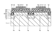
次に、図14に示すように、図7〜図11に示した第1参考形態と同様のプロセスを用いて、[1−100]方向(図13参照)に延びるリッジ部31を形成した後、開口部32aを有する電流ブロック層32(図15参照)、p側オーミック電極33およびp側パッド電極34を順次形成する。また、n型GaN基板21の裏面上の所定領域に、n側オーミック電極15およびn側パッド電極16を順次形成する。なお、図14の断面図は、[1−100]方向に延びる線に沿った断面図である。この第2参考形態では、溝部21aが[11−20]方向(図13参照)に延びるように形成されているので、[1−100]方向に延びるリッジ部31は、溝部21aと直交する。また、リッジ部31は、電流通路になるとともに、リッジ部31の下方が発光部分となる。また、電流ブロック層32、p側オーミック電極33およびp側パッド電極34を形成する際には、上記第1参考形態の電流ブロック層12、p側オーミック電極13およびp側パッド電極14と同じ厚みおよび組成となるように形成する。
Next, as shown in FIG. 14, after forming the
この後、図14に示した構造体において、[1−100]方向(図13参照)に素子分離するとともに、[11−20]方向(図13参照)に素子を各チップに劈開する。この際、劈開されたチップの劈開面間の距離(図14の共振器長L)が、溝部21a間の距離W12(図13参照)よりも小さくなるように、n型GaN基板21の領域21bに対応する所定領域(図14の破線に対応する領域)を[11−20]方向に沿って劈開する。これにより、図15に示すような第2参考形態による窒化物系半導体レーザ素子が形成される。
Thereafter, in the structure shown in FIG. 14, the elements are separated in the [1-100] direction (see FIG. 13), and the elements are cleaved in the chips in the [11-20] direction (see FIG. 13). At this time, the
なお、図15に示すように、第2参考形態の製造プロセスにより形成された窒化物系半導体レーザ素子では、上記した劈開工程により溝部21aに対応する部分が全て除去されている。このため、第2参考形態による窒化物系半導体レーザ素子では、上記第1参考形態の窒化物系半導体レーザ素子と異なり、n型GaN基板21に段差部が存在しない。
As shown in FIG. 15, in the nitride semiconductor laser element formed by the manufacturing process of the second reference embodiment, all the portions corresponding to the
第2参考形態では、上記のように、n型GaN基板21上にバッファ層22を介して窒化物系半導体素子層30を形成する際に、溝部21aの側面上に形成されるn型Al0.07Ga0.93Nからなるn型クラッド層23の厚みが、n型GaN基板21の領域21b上に形成されるn型クラッド層23の厚みよりも小さくなるように形成することによって、上記第1参考形態と同様、n型クラッド層23に生じる歪みが溝部21aの側面上に位置するn型クラッド層23の厚みが小さい部分に集中するので、n型GaN基板21の領域21b上に位置するn型クラッド層23に発生するクラック39a〜39cの量が増大するのを抑制することができるとともに、n型クラッド層23を含む窒化物系半導体素子層30に発生するクラック39a〜39cの量が増大するのも抑制することができる。その結果、上記第1参考形態と同様、クラック39a〜39cによりリーク電流が増大するとともに、クラック39a〜39cにより光導波が妨げられるという不都合が発生するのを抑制することができるので、窒化物系半導体レーザ素子の特性および歩留りの低下を抑制することができる。
In the second reference embodiment, as described above, when the nitride-based
また、第2参考形態では、n型GaN基板21に溝部21aを形成する際に、溝部21aが[11−20]方向に延びるように形成することによって、[1−210]方向に延びるように発生するクラック39bおよび[−2110]方向に延びるように発生するクラック39cが、[11−20]方向に延びる溝部21aに対応する領域と交差するので、クラック39bおよび39cが溝部21aに対応する領域を横切って伝播するのを抑制することができる。
In the second reference embodiment, when the
なお、第2参考形態のその他の効果は、上記第1参考形態と同様である。 The remaining effects of the second reference embodiment are the same as those of the first reference embodiment.
(第3参考形態)
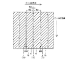
図16は、本発明の第3参考形態による窒化物系半導体レーザ素子の製造プロセスを説明するための平面図である。図16および図26を参照して、この第3参考形態では、上記第1および第2参考形態と異なり、n型GaN基板に、[1−100]方向および[11−20]方向の2方向に延びるストライプ状(細長状)の溝部を格子状に形成する場合について説明する。
(3rd reference form)
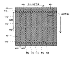
Figure 16 is a plan view for explaining the manufacturing process of the third referential embodiment nitride by based semiconductor laser device of the present invention. Referring to FIGS. 16 and 26, in the third reference embodiment, unlike the first and second reference embodiments, two directions of [1-100] direction and [11-20] direction are applied to the n-type GaN substrate. A case where stripe-like (elongated) groove portions extending in a grid pattern are formed will be described.
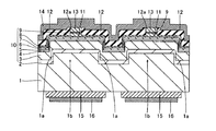
この第3参考形態による窒化物系半導体レーザ素子の製造プロセスでは、図16に示すように、まず、図1〜図4に示した第1参考形態と同様のプロセスを用いて、n型GaN基板41に、約50μmの幅W21と、約2μmの深さとを有するとともに、n型GaN基板41の上面に対して垂直な側面を有するストライプ状(細長状)の溝部41aおよび41bを形成する。ただし、この第3参考形態では、溝部41aを[1−100]方向に延びるように形成し、かつ、溝部41bを[11−20]方向に延びるように形成することによって、溝部41aおよび41bを格子状に配置する。また、[11−20]方向に隣接する溝部41a間の距離W22を、約200μmに設定する。また、[1−100]方向に隣接する溝部41b間の距離W23を、後の劈開工程において形成される劈開面間の距離(共振器長)よりも大きい距離に設定する。そして、n型GaN基板41において、溝部41aおよび41bに囲まれた領域41cは、後述する窒化物系半導体素子層40のリッジ部(図示せず)の下方に位置する発光部分に対応する領域となる。なお、n型GaN基板41は、本発明の「窒化物系半導体基板」の一例である。また、n型GaN基板41の領域41cは、本発明の「第1領域」の一例であり、n型GaN基板41の溝部41aおよび41bが形成された領域は、本発明の「第2領域」の一例である。
In the third manufacturing process for the nitride-based semiconductor laser device according to Reference Embodiment, as shown in FIG. 16, first, a process similar to that of the first reference embodiment shown in FIGS. 1 to 4, n-
なお、第3参考形態のn型GaN基板41は、上記第1参考形態のn型GaN基板1と同様、(0001)面の表面を有するとともに、低い転位密度を有する。また、n型GaN基板41は、約0.3189nmの格子定数を有する。
Note that the n-
この後、図6に示した第1参考形態と同様のプロセスを用いて、n型GaN基板41の領域41cの上面上、溝部41aおよび41bの各々の底面および側面上に、バッファ層(図示せず)を介して、窒化物系半導体素子層40を形成する。なお、窒化物系半導体素子層40を形成する際には、上記第1参考形態の窒化物系半導体素子層10と同じ構造を有するように形成する。すなわち、第3参考形態の製造プロセスにより形成された窒化物系半導体素子層40は、n型GaN基板41上にバッファ層を介して形成されたn型クラッド層(図示せず)を含む。また、窒化物系半導体素子層40を構成するn型クラッド層は、n型Al0.07Ga0.93Nからなるとともに、約0.3184nmの格子定数を有する。
Thereafter, a buffer layer (not shown) is formed on the upper surface of the
この際、第3参考形態では、上記第1参考形態と同様、[1−100]方向に延びる溝部41aおよび[11−20]方向に延びる溝部41bの各々の側面上に形成された窒化物形半導体各層の厚みは、n型GaN基板41の領域41c上に形成された窒化物系半導体各層の厚みよりも小さくなる。このため、窒化物系半導体素子層40を構成するn型クラッド層に生じる歪みが溝部41aおよび41bの各々の側面上に位置するn型クラッド層の厚みが小さい部分に集中するので、n型GaN基板41の領域41c上に位置するn型クラッド層に生じる歪みを小さくすることができる。これにより、n型クラッド層に発生するクラック49a〜49cの量が増大するのが抑制されるとともに、n型クラッド層を含む窒化物系半導体素子層40に発生するクラック49a〜49cの量が増大するのも抑制される。
At this time, in the third reference embodiment, as in the first reference embodiment, the nitride shape formed on each side surface of the
また、第3参考形態では、[11−20]方向に延びるように発生するクラック49a、[1−210]方向(図26参照)に延びるように発生するクラック49bおよび[−2110]方向(図26参照)に延びるように発生するクラック49cが、[1−100]方向に延びる溝部41aに対応する領域と交差するので、クラック49a〜49cが溝部41aに対応する領域を横切って伝播するのが抑制される。さらに、[1−210]方向に延びるように発生するクラック49bおよび[−2110]方向に延びるように発生するクラック49cは、[11−20]方向に延びる溝部41bに対応する領域とも交差するので、クラック49bおよび49cが溝部41bに対応する領域を横切って伝播するのも抑制される。
Further, in the third reference embodiment, the
なお、第3参考形態のこの後の製造プロセスは、上記第1参考形態と同様である。すなわち、第3参考形態の窒化物系半導体素子層40には、[11−20]方向に延びる溝部41bと直交し、かつ、溝部41aの延びる方向と同じ[1−100]方向に延びるリッジ部(図示せず)が形成される。
The manufacturing process after this the third reference embodiment are the same as those of the first reference embodiment. That is, in the nitride-based
第3参考形態では、上記のように、n型GaN基板41上にバッファ層を介して窒化物系半導体素子層40を形成する際に、溝部41aおよび41bの各々の側面上に形成されるn型Al0.07Ga0.93Nからなるn型クラッド層の厚みが、n型GaN基板41の領域41c上に形成されるn型クラッド層の厚みよりも小さくなるように形成することによって、上記第1参考形態と同様、n型クラッド層に生じる歪みが溝部41aおよび41bの各々の側面上に位置するn型クラッド層の厚みが小さい部分に集中するので、n型GaN基板41の領域41c上に位置するn型クラッド層に発生するクラック49a〜49cの量が増大するのを抑制することができるとともに、n型クラッド層を含む窒化物系半導体素子層40に発生するクラック49a〜49cの量が増大するのも抑制することができる。その結果、上記第1参考形態と同様、クラック49a〜49cによりリーク電流が増大するとともに、クラック49a〜49cにより光導波が妨げられるという不都合が発生するのを抑制することができるので、窒化物系半導体レーザ素子の特性および歩留りの低下を抑制することができる。
In the third reference embodiment, as described above, when the nitride-based
また、第3参考形態では、n型GaN基板41に、[1−100]方向および[11−20]方向の2方向に延びるストライプ状(細長状)の溝部41aおよび41bを格子状に形成することによって、[11−20]方向に延びるように発生するクラック49a、[1−210]方向に延びるように発生するクラック49bおよび[−2110]方向に延びるように発生するクラック49cが、[1−100]方向に延びる溝部41aに対応する領域と交差するので、クラック49a〜49cが溝部41aに対応する領域を横切って伝播するのを抑制することができる。さらに、[1−210]方向に延びるように発生するクラック49bおよび[−2110]方向に延びるように発生するクラック49cは、[11−20]方向に延びる溝部41bに対応する領域とも交差するので、クラック49bおよび49cが溝部41bに対応する領域を横切って伝播するのも抑制することができる。
In the third reference embodiment, striped (elongated)
なお、第3参考形態のその他の効果は、上記第1参考形態と同様である。 The remaining effects of the third reference embodiment are similar to those of the aforementioned first reference embodiment.
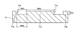
(第4参考形態)
図17〜図19は、本発明の第4参考形態による窒化物系半導体レーザ素子の製造プロセスを説明するための断面図である。図20は、本発明の第4参考形態による窒化物系半導体レーザ素子の製造プロセスを用いて形成された窒化物系半導体レーザ素子の構造を示した断面図である。図17〜図20および図26を参照して、この第4参考形態では、上記第1〜第3参考形態と異なり、n型GaN基板に形成する溝部の開口幅を、溝部の底面から開口端に向かって徐々に大きくする場合について説明する。
(4th reference form)
17 to 19 are cross-sectional views for explaining a manufacturing process of a fourth reference embodiment nitride by based semiconductor laser device of the present invention. Figure 20 is a fourth cross-sectional view showing a structure of a nitride-based semiconductor laser device formed by the manufacturing process for the nitride-based semiconductor laser device according to another embodiment of the present invention. With reference to FIGS. 17 to 20 and FIG. 26, in the fourth reference embodiment, unlike the first to third reference embodiments, the opening width of the groove portion formed in the n-type GaN substrate is changed from the bottom surface of the groove portion to the opening end. A case of gradually increasing toward will be described.
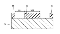
この第4参考形態による窒化物系半導体レーザ素子の製造プロセスでは、図17に示すように、まず、(0001)面の表面を有するとともに、低い転位密度を有するn型GaN基板51を準備する。このn型GaN基板51は、約0.3189nmの格子定数を有する。なお、n型GaN基板51は、本発明の「窒化物系半導体基板」の一例である。そして、プラズマCVD法を用いて、n型GaN基板51上の所定領域に、約0.5μmの厚みを有するSiO2膜からなるストライプ状(細長状)のマスク層65を形成する。具体的には、マスク層65が、所定の方向(たとえば、[1−100]方向)に延びるように形成する。また、隣接するマスク層65間の距離W31を、約50μmに設定するとともに、マスク層65の幅W32を、約200μmに設定する。
In the fourth manufacturing process for the nitride-based semiconductor laser device according to Reference Embodiment, as shown in FIG. 17, first, and has a surface of (0001) plane, to prepare the n-
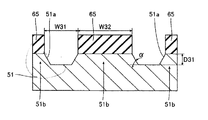
次に、図18に示すように、Cl2ガスによるRIE法を用いて、マスク層65をエッチングマスクとして、n型GaN基板51の上面から約2μmの深さまでをエッチングする。なお、この場合のエッチング選択比(マスク層65/n型GaN基板51)は、1:10である。また、エッチング条件としては、エッチング圧力:約3.325kPa、プラズマパワー:約200W、エッチング速度:約140nm/sec〜約150nm/secである。これにより、n型GaN基板51に、約50μmの幅(開口端の幅)W31と、約2μmの深さD31とを有するとともに、所定の方向([1−100]方向)に延びるストライプ状(細長状)の溝部51aが形成される。なお、エッチングマスクとしてSiO2膜からなるマスク層65を用いるとともに、上記したエッチング条件でn型GaN基板51をエッチングした場合、溝部51aの断面形状は、メサ形状となる。すなわち、溝部51aの開口幅が、溝部51aの底面から開口端に向かって徐々に大きくなる。具体的には、溝部51aの底面と側面とがなす角度αが、約40°となる。そして、n型GaN基板51において、溝部51aに挟まれた約200μmの幅W32を有する領域51bは、後述する窒化物系半導体素子層60の発光部分に対応する領域となる。なお、n型GaN基板51の領域51bは、本発明の「第1領域」の一例であり、n型GaN基板51の溝部51aが形成された領域は、本発明の「第2領域」の一例である。この後、マスク層65を除去する。
Next, as shown in FIG. 18, the RIE method using Cl 2 gas is used to etch from the upper surface of the n-
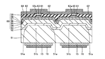
次に、図19に示すように、図6に示した第1参考形態と同様のプロセスを用いて、n型GaN基板51の領域51bの上面上、溝部51aの底面および側面上に、バッファ層52を介して、窒化物系半導体素子層60を形成する。この際、n型GaN基板51側から順に、バッファ層52、n型クラッド層53、n側キャリアブロック層54、MQW活性層55、p側光ガイド層56、p側キャリアブロック層57、p型クラッド層58およびp側コンタクト層59を形成する。なお、上記した各層(52〜59)を形成する際には、上記第1参考形態の窒化物系半導体各層(2〜9)と同じ厚みおよび組成となるように形成する。すなわち、n型GaN基板51上にバッファ層52を介して形成されるn型クラッド層53は、n型Al0.07Ga0.93Nにより構成され、かつ、約0.3184nmの格子定数を有するように形成される。なお、n型クラッド層53は、本発明の「窒化物系半導体層」の一例である。
Next, as shown in FIG. 19, a buffer layer is formed on the upper surface of the
ここで、第4参考形態では、溝部51aの断面形状がメサ形状であることにより、n型GaN基板51上にバッファ層52を介してn型Al0.07Ga0.93Nからなるn型クラッド層53を形成する際に、n型クラッド層53の構成材料の一部であるGaが溝部51aの傾斜した側面側へ移動しやすくなると考えられる。このため、溝部51aの側面上に形成されるn型クラッド層53のAl組成比が、n型GaN基板51の領域51b上に形成されるn型クラッド層53のAl組成比よりも低くなる。具体的には、n型GaN基板51の領域51b上に形成されるn型クラッド層53のAl組成比が約7%であるのに対して、溝部51aの側面上に形成されるn型クラッド層53のAl組成比が約6.6%となる。この場合、溝部51aの側面上に位置するn型クラッド層53のAl組成比が低い部分の格子定数がn型GaN基板51の格子定数に近づくので、溝部51aの側面上に位置するn型クラッド層53のAl組成比が低い部分において、n型GaN基板51とn型クラッド層53との間の格子定数差が小さくなる。このため、約0.3189nmの格子定数を有するn型GaN基板51と、約0.3184nmの格子定数を有するn型Al0.07Ga0.93Nからなるn型クラッド層53との間の格子定数差に起因してn型クラッド層53に歪みが生じたとしても、その歪みが溝部51aの側面上に位置するn型クラッド層53のAl組成比が低い部分において緩和されるので、n型クラッド層53に生じる歪みが小さくなる。これにより、n型クラッド層53に発生するクラックの量が増大するのが抑制されるとともに、n型クラッド層53を含む窒化物系半導体素子層60に発生するクラックの量が増大するのも抑制される。
Here, in the fourth reference embodiment, since the cross-sectional shape of the
この後、図7〜図11に示した第1参考形態と同様のプロセスを用いて、[1−100]方向(図26参照)に延びるリッジ部61を形成した後、開口部62aを有する電流ブロック層62、p側オーミック電極63およびp側パッド電極64を順次形成する。また、n型GaN基板51の裏面上の所定領域に、n側オーミック電極15およびn側パッド電極16を順次形成する。なお、第4参考形態では、溝部51aが[1−100]方向(図26参照)に延びるように形成されているので、[1−100]方向に延びるリッジ部61は、溝部51aとは交差しない。このリッジ部61は、電流通路になるとともに、このリッジ部61の下方が発光部分となる。また、電流ブロック層62、p側オーミック電極63およびp側パッド電極64を形成する際には、上記第1参考形態の電流ブロック層12、p側オーミック電極13およびp側パッド電極14と同じ厚みおよび組成となるように形成する。
Thereafter, a
この後、上記第1参考形態と同様の素子分離および劈開を行うことによって、図20に示すような第4参考形態による窒化物系半導体レーザ素子が形成される。 Thereafter, element isolation and cleavage similar to those of the first reference embodiment are performed, so that a nitride-based semiconductor laser device according to the fourth reference embodiment as shown in FIG. 20 is formed.
なお、図20に示すように、第4参考形態の製造プロセスにより形成された窒化物系半導体レーザ素子において、n型GaN基板51の溝部51a(図19参照)は、上記した素子分離工程により傾斜した側面を有する段差部51cとなる。すなわち、第4参考形態の製造プロセスにより形成された窒化物系半導体レーザ素子では、n型GaN基板51の段差部51cの側面上に形成されたn型クラッド層53のAl組成比が、n型GaN基板51の領域51b上に形成されたn型クラッド層53のAl組成比よりも低くなる。
As shown in FIG. 20, in the nitride-based semiconductor laser device formed by the manufacturing process of the fourth reference embodiment, the
第4参考形態では、上記のように、n型GaN基板51上にバッファ層52を介して窒化物系半導体素子層60を形成する際に、溝部51aの側面上に形成されるn型クラッド層53のAl組成比が、n型GaN基板51の領域51b上に形成されるn型クラッド層53のAl組成比よりも低くなるように形成することによって、約0.3189nmの格子定数を有するn型GaN基板51と、約0.3184nmの格子定数を有するn型Al0.07Ga0.93Nからなるn型クラッド層53との間の格子定数差に起因してn型クラッド層53に歪みが生じたとしても、その歪みが溝部51aの側面上に位置するn型クラッド層53のAl組成比が低い部分において緩和されるので、n型クラッド層53に生じる歪みを小さくすることができる。これにより、n型クラッド層53に生じる歪みが大きいことに起因して、n型クラッド層53に発生するクラックの量が増大するという不都合が発生するのを抑制することができる。したがって、n型クラッド層53を含む窒化物系半導体素子層60に発生するクラックの量が増大するのを抑制することができるので、クラックにより窒化物系半導体素子層60の発光部分に供給されないリーク電流が増大するとともに、クラックにより光導波が妨げられるという不都合が発生するのを抑制することができる。その結果、窒化物系半導体レーザ素子の特性および歩留りの低下を抑制することができる。
In the fourth reference embodiment, as described above, when the nitride-based
また、第4参考形態では、n型GaN基板51に溝部51aを形成する際に、溝部51aの開口幅が溝部51aの底面から開口端に向かって徐々に大きくなるように形成することによって、n型GaN基板51上にバッファ層52を介してn型Al0.07Ga0.93Nからなるn型クラッド層53を形成する際に、n型クラッド層53の構成材料の一部であるGaがAlに比べて成膜表面を移動しやすいことにより、Gaが溝部51aの側面側へ移動しやすくなると考えられるので、容易に、溝部51aの側面上に形成されるn型クラッド層53のAl組成比を、n型GaN基板51の領域51b上に形成されるn型クラッド層53のAl組成比よりも小さくすることができる。
In the fourth reference embodiment, when the
なお、第4参考形態のその他の効果は、上記第1参考形態と同様である。 The remaining effects of the fourth reference embodiment are similar to those of the aforementioned first reference embodiment.
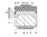
(第5参考形態)
図21は、本発明の第5参考形態による窒化物系半導体レーザ素子の製造プロセスを説明するための断面図である。図21を参照して、この第5参考形態では、上記第4参考形態と異なり、n型GaN基板に形成する溝部の開口幅を、溝部の底面から開口端に向かって徐々に小さくする場合について説明する。
(5th reference form)
Figure 21 is a sectional view for explaining the manufacturing process of the fifth reference embodiment nitride by based semiconductor laser device of the present invention. Referring to FIG. 21, in the fifth reference embodiment, unlike the fourth reference embodiment, the opening width of the groove portion formed in the n-type GaN substrate is gradually reduced from the bottom surface of the groove portion toward the opening end. explain.
この第5参考形態による窒化物系半導体レーザ素子の製造プロセスでは、図21に示すように、まず、図1〜図4に示した第1参考形態と同様のプロセスを用いて、n型GaN基板71に、約2μmの深さD41を有するとともに、所定の方向に延びるストライプ状(細長状)の溝部71aを形成する。ただし、この第5参考形態では、n型GaN基板71に溝部71aを形成する際に、エッチング装置の基台(図示せず)にn型GaN基板71を斜めに設置するとともに、n型GaN基板71を回転させながらエッチングすることによって、溝部71aの断面形状が逆メサ形状になるように形成する。すなわち、溝部71aの開口幅が、溝部71aの底面から開口端に向かって徐々に小さくなるように形成する。具体的には、溝部71aの開口端の幅W41が約50μmになるように、かつ、溝部71aの底面の幅W42が約53μmになるように形成する。また、隣接する溝部71a間の距離W43を、約200μmに設定する。そして、n型GaN基板71において、溝部71aに挟まれた約200μmの幅W43を有する領域71bは、窒化物系半導体素子層のリッジ部(図示せず)の下方に位置する発光部分に対応する領域となる。なお、n型GaN基板71は、本発明の「窒化物系半導体基板」の一例である。また、n型GaN基板71の領域71bは、本発明の「第1領域」の一例であり、n型GaN基板71の溝部71aが形成された領域は、本発明の「第2領域」の一例である。
In the manufacturing process of the nitride-based semiconductor laser device according to the fifth reference embodiment, as shown in FIG. 21, first, an n-type GaN substrate is manufactured using the same process as that of the first reference embodiment shown in FIGS. 71 is formed with a stripe-shaped (elongated)
なお、第5参考形態のn型GaN基板71は、上記第1参考形態のn型GaN基板1と同様、(0001)面の表面を有するとともに、低い転位密度を有する。また、n型GaN基板71は、約0.3189nmの格子定数を有する。
Note that the n-
なお、第5参考形態のこの後の製造プロセスは、上記第1参考形態と同様である。 The manufacturing process after this the fifth reference embodiment are the same as those of the first reference embodiment.
第5参考形態では、上記のように、n型GaN基板71に溝部71aを形成する際に、溝部71aの開口幅が溝部71aの底面から開口端に向かって徐々に小さくなるように形成することによって、n型GaN基板71上に窒化物系半導体層を形成する際に、溝部1aの側面がn型GaN基板1の上面に対して垂直である第1参考形態に比べて、窒化物系半導体層の構成材料が溝部71aの側面上に堆積されにくくなるので、より容易に、溝部71aの側面上に形成される窒化物系半導体層の厚みを、n型GaN基板71の領域71b上に形成される窒化物系半導体層の厚みよりも小さくすることができる。
In the fifth reference embodiment, as described above, when the
なお、第5参考形態のその他の効果は、上記第1参考形態と同様である。 The remaining effects of the fifth reference embodiment are similar to those of the aforementioned first reference embodiment.
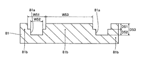
(第6参考形態)
図22は、本発明の第6参考形態による窒化物系半導体レーザ素子の製造プロセスを説明するための断面図である。図22を参照して、この第6参考形態では、上記第4および第5参考形態と異なり、n型GaN基板に形成される溝部の側面が段差部を有する場合について説明する。
(6th reference form)
Figure 22 is a sectional view for explaining the manufacturing process of the sixth referential embodiment nitride by based semiconductor laser device of the present invention. Referring to FIG. 22, in the sixth reference embodiment, unlike the fourth and fifth reference embodiments, a case where the side surface of the groove formed in the n-type GaN substrate has a stepped portion will be described.
この第6参考形態による窒化物系半導体レーザ素子の製造プロセスでは、図22に示すように、まず、図1〜図4に示した第1参考形態と同様のプロセスを用いて、n型GaN基板81に、所定の方向に延びるストライプ状(細長状)の溝部81aを形成する。ただし、この第6参考形態では、溝部81aを形成するためのエッチング工程を2回行う。具体的には、1回目のエッチング工程で、約50μmの幅W51と、約1μmの深さD51とを有する1つ目の溝部を形成する。この後、2回目のエッチング工程で、1回目のエッチング工程で形成された1つ目の溝部の底部に、約30μmの幅W52と、約1μmの深さD52とを有する2つ目の溝部を形成する。これにより、n型GaN基板81に、約50μmの幅(開口端の幅)W51と、約2μmの深さD53とを有するとともに、側面が段差部を有する溝部81aが形成される。また、隣接する溝部81a間の距離W53を、約200μmに設定する。そして、n型GaN基板81において、溝部81aに挟まれた約200μmの幅W53を有する領域81bは、窒化物系半導体素子層のリッジ部(図示せず)の下方に位置する発光部分に対応する領域となる。なお、n型GaN基板81は、本発明の「窒化物系半導体基板」の一例である。また、n型GaN基板81の領域81bは、本発明の「第1領域」の一例であり、n型GaN基板81の溝部81aが形成された領域は、本発明の「第2領域」の一例である。
In the manufacturing process of the nitride-based semiconductor laser device according to the sixth reference embodiment, as shown in FIG. 22, first, an n-type GaN substrate is manufactured using the same process as that of the first reference embodiment shown in FIGS. In 81, a striped (elongated)
なお、第6参考形態のn型GaN基板81は、上記第1参考形態のn型GaN基板1と同様、(0001)面の表面を有するとともに、低い転位密度を有する。また、n型GaN基板81は、約0.3189nmの格子定数を有する。
The n-
なお、第6参考形態のこの後の製造プロセスは、上記第1参考形態と同様である。 The manufacturing process after this the sixth reference embodiment are the same as those of the first reference embodiment.
第6参考形態では、上記のように、n型GaN基板に所定の方向に延びるストライプ状(細長状)の溝部81aを形成し、かつ、その溝部81aの側面に段差部を設けることによって、上記第1参考形態と同様の効果を得ることができる。
In the sixth reference embodiment, as described above, the stripe-shaped (elongated)
なお、今回開示された実施形態は、すべての点で例示であって制限的なものではないと考えられるべきである。本発明の範囲は、上記した実施形態の説明ではなく特許請求の範囲によって示され、さらに特許請求の範囲と均等の意味および範囲内でのすべての変更が含まれる。 The embodiment disclosed this time should be considered as illustrative in all points and not restrictive. The scope of the present invention is shown not by the above description of the embodiments but by the scope of claims for patent, and further includes all modifications within the meaning and scope equivalent to the scope of claims for patent.
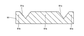
たとえば、上記第1〜第6参考形態及び以下に示す第7、第8実施形態では、n型GaN基板を用いたが、本発明はこれに限らず、p型窒化物系半導体基板を用いるとともに、p型窒化物系半導体基板上に、p型窒化物系半導体層、活性層およびn型窒化物系半導体層を順次形成するようにしてもよい。 For example, in the first to sixth reference embodiments and the seventh and eighth embodiments described below, the n-type GaN substrate is used. However, the present invention is not limited to this, and a p-type nitride semiconductor substrate is used. A p-type nitride semiconductor layer, an active layer, and an n-type nitride semiconductor layer may be sequentially formed on the p-type nitride semiconductor substrate.
また、上記第1〜第6参考形態及び以下に示す第7、第8実施形態では、GaN基板を用いたが、本発明はこれに限らず、GaN基板以外の窒化物系半導体基板を用いてもよい。GaN基板以外の窒化物系半導体基板としては、たとえば、AlGaN、AlN、AlGaInNまたはAlGaInBNからなる窒化物系半導体基板がある。 In the first to sixth reference embodiments and the seventh and eighth embodiments described below, the GaN substrate is used. However, the present invention is not limited to this, and a nitride semiconductor substrate other than the GaN substrate is used. Also good. Examples of the nitride semiconductor substrate other than the GaN substrate include a nitride semiconductor substrate made of AlGaN, AlN, AlGaInN, or AlGaInBN.
また、上記第1〜第6参考形態及び以下に示す第7、第8実施形態では、n型GaN基板に、底面を有する溝部を形成するようにしたが、本発明はこれに限らず、n型GaN基板に、底面を有しない溝部を形成してもよい。たとえば、図23に示すように、n型GaN基板91に、断面形状がV字状の溝部91aを形成してもよい。なお、n型GaN基板91は、本発明の「窒化物系半導体基板」の一例である。このように構成すれば、上記第4参考形態と同様、MOCVD法などを用いてn型GaN基板91上にAlGaN層を形成する際に、AlGaN層の構成材料であるGaがV字状の断面形状を有する溝部91aの内面側へ移動しやすくなると考えられる。これにより、容易に、溝部91aの内面上に形成されるAlGaN層のAl組成比を、溝部91a以外の領域上に形成されるAlGaN層のAl組成比よりも低くすることができる。また、n型GaN基板91の溝部91aが形成された領域以外の領域91bは、窒化物系半導体素子層のリッジ部の下方に位置する発光部分に対応する領域となる。なお、n型GaN基板91の領域91bは、本発明の「第1領域」の一例であり、n型GaN基板91の溝部91aが形成された領域は、本発明の「第2領域」の一例である。
In the first to sixth reference embodiments and the seventh and eighth embodiments described below, the groove portion having the bottom surface is formed in the n-type GaN substrate. However, the present invention is not limited to this. A groove portion having no bottom surface may be formed in the type GaN substrate. For example, as shown in FIG. 23, a
また、上記第1〜第6参考形態及び以下に示す第7、第8実施形態では、窒化物系半導体各層の結晶成長を、MOCVD法を用いて行ったが、本発明はこれに限らず、HVPE(Hydride Vapor Phase Epitaxy)法、および、TMAl、TMGa、TMIn、NH3、ヒドラジン、SiH4、GeH4およびMg(C5H5)などを原料ガスとして用いるガスソースMBE(Molecular Beam Epitaxy)法などを用いて結晶成長を行ってもよい。 Further, in the first to sixth reference embodiments and the seventh and eighth embodiments described below, the crystal growth of each nitride-based semiconductor layer is performed using the MOCVD method, but the present invention is not limited thereto, HVPE (Hydride Vapor Phase Epitaxy) method and gas source MBE (Molecular Beam Epitaxy) method using TMAl, TMGa, TMIn, NH 3 , hydrazine, SiH 4 , GeH 4 and Mg (C 5 H 5 ) as raw material gas For example, crystal growth may be performed.
また、上記第1〜第6参考形態及び以下に示す第7、第8実施形態では、GaN基板の(0001)面上に、窒化物系半導体層を形成したが、本発明はこれに限らず、GaN基板の他の面方位の面上に、窒化物系半導体層を形成してもよい。たとえば、(1−100)や(11−20)面などの(H、K、−H−K、0)面上に、窒化物系半導体層を形成してもよい。この場合、発光層にピエゾ電場が発生しないので、発光層の発光効率を向上させることができる。以下に、この一例である第7、第8実施形態について説明する。 In the first to sixth reference embodiments and the seventh and eighth embodiments described below, the nitride-based semiconductor layer is formed on the (0001) plane of the GaN substrate. However, the present invention is not limited to this. A nitride-based semiconductor layer may be formed on the surface of the other surface orientation of the GaN substrate. For example, a nitride-based semiconductor layer may be formed on (H, K, -HK, 0) planes such as the (1-100) and (11-20) planes. In this case, since no piezoelectric field is generated in the light emitting layer, the light emission efficiency of the light emitting layer can be improved. The seventh and eighth embodiments, which are examples of this, will be described below.
(第7実施形態)
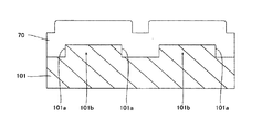
図27は、本発明の第7実施形態に係る窒化物系半導体レーザ素子を説明するための平面図であり、図28は図27における400−400線に沿った断面図である。本実施形態に係る窒化物系半導体レーザ素子が第1参考形態に係る半導体レーザ素子と異なる点は、基板として(11−20)面の表面を有するn型GaN基板101を用いる点、及び溝部101aが[1−100]方向に延びるように形成されている点である。
(Seventh embodiment)
FIG. 27 is a plan view for explaining a nitride-based semiconductor laser device according to the seventh embodiment of the present invention, and FIG. 28 is a cross-sectional view taken along the line 400-400 in FIG. The nitride semiconductor laser device according to this embodiment is different from the semiconductor laser device according to the first reference embodiment in that an n-
本実施形態においても、図1〜図4に示した第1参考形態と同様のプロセスを用いて、n型GaN基板101に、約50μmの幅W71と、約2μmの深さとを有するとともに、n型GaN基板101の上面に対して垂直な側面を有するストライプ状(細長状)の溝部101aが形成されている。ただし、前述の通り本実施形態においてはn型GaN基板101が(11−20)面を有しており、溝部101aは[1−100]方向に延びるように形成されている。
Also in this embodiment, by using a process similar to that of the first reference embodiment shown in FIGS. 1 to 4, the n-
そして、n型GaN基板上101上には、第1参考形態と同様のプロセスを用いて窒化物系半導体素子層70が形成されている。この窒化物系半導体素子層70は、第1参考形態と同様に、基板101側からn型クラッド層、活性層、p型クラッド層を有している。
A nitride-based
窒化物系半導体素子層70に含まれるn型クラッド層には一般にAlGaN層が用いられており、このAlGaN層とn型GaN基板との格子定数差は基板の結晶軸の方向によって異なっている。例えば、Al0.07Ga0.93NとGaNのa軸方向の格子定数は夫々約0.3184nm、約0.3189nmであり、その比は0.9984である。一方c軸方向の格子定数は夫々約0.5172nm,0.5186nmであり、その比は0.9973である。このようにAl0.07Ga0.93NとGaNの格子定数比はa軸方向で0.9984、c軸方向で0.9973であり、c軸方向の方が1からのずれが大きい。このため、面内の軸方向がa軸だけの(0001)面を有するGaN基板を用いた第1〜第6参考形態に比べ、面内の軸方向としてc軸方向を含む(11−20)面を有するGaN基板を用いた本実施形態の方が、AlGaN層に加わる歪みや応力が大きくなる。このため本実施形態に係る窒化物系半導体レーザ素子では、第1〜第6参考形態に係る窒化物系半導体レーザ素子に比べ、AlGaN層にクラックが発生しやすく、その結果窒化物系半導体素子層70にクラックが発生し易い。
An AlGaN layer is generally used as the n-type cladding layer included in the nitride-based
そこで、本願にあっては基板101に設ける溝部101aを[1−100]方向に延びるように設けている。
Therefore, in the present application, the
即ち、[1−100]方向はm軸方向に相当し、結晶構造的にm軸方向の歪み或いは応力の大きさはa軸方向の歪みあるいは応力の大きさと略等しい。従って、(11−20)面を有する基板を用いた場合にあっては、[1−100]m軸方向よりも[0001]c軸方向の方が歪み或いは応力が大きいため、[1−100]方向と交差する方向よりも、[0001]方向と交差する方向にクラックが発生し易い。従って、本実施形態のように[0001]方向と交差する[1−100]軸方向に沿って溝部101aを設けることにより、[0001]方向と交差する方向に発生するクラックの伝搬を効果的に抑制することができる。このように、本実施形態においては多数のクラックが発生する方向のクラックの伝搬を抑制するようにしたので、より大きな効果が得られる。
That is, the [1-100] direction corresponds to the m-axis direction, and the strain or stress in the m-axis direction is approximately equal to the strain or stress in the a-axis direction in terms of crystal structure. Therefore, when a substrate having a (11-20) plane is used, the strain or stress is larger in the [0001] c-axis direction than in the [1-100] m-axis direction. ] Cracks are more likely to occur in the direction intersecting the [0001] direction than in the direction intersecting the [0001] direction. Therefore, by providing the
また、本実施形態においては、第4参考形態のように、n型GaN基板に形成する溝部の開口幅を、溝部の底面から開口端に向かって徐々に大きくすることが好ましい。このように溝部101aの断面形状がメサ形状であることにより、n型GaN基板101上にAlGaN層を含む窒化物半導体素子層70を形成する際に、AlGaN層の構成材料の一部であるGaが溝部101aの傾斜した側面側へ移動しやすくなると考えられる。このため、溝部101aの側面上に形成されるAlGaN層のAl組成比が、n型GaN基板101の領域101b上に形成されるAlGaN層のAl組成比よりも低くなる。具体的には、AlGaN層としてAl組成比が約7%の層を形成する場合、n型GaN基板101の領域101b上に形成されるAlGaN層のAl組成比が約7%であるのに対して、溝部101aの側面上に形成されるAlGaN層のAl組成比が約1.4%となる。この場合、溝部101aの側面上に位置するAlGaN層のAl組成比が低い部分の格子定数がn型GaN基板101の格子定数に近づくので、溝部101aの側面上に位置するAlGaN層のAl組成比が低い部分において、n型GaN基板101とAlGaN層との間の格子定数差が小さくなる。このため、n型GaN基板101と、窒化物半導体素子層70中のAlGaN層との間の格子定数差に起因してAlGaN層に歪みが生じたとしても、その歪みが溝部101aの側面上に位置するAlGaN層のAl組成比が低い部分において緩和されるので、AlGaN層に生じる歪みが小さくなる。これにより、AlGaN層に発生するクラックの量が増大するのが抑制されるとともに、AlGaN層を含む窒化物系半導体素子層70に発生するクラックの量が増大するのも抑制される。
(第8実施形態)
図29は、本発明の第8実施形態に係る窒化物系半導体レーザ素子を説明するための平面図であり、図30は図29における500−500線に沿った断面図である。本実施形態に係る窒化物系半導体レーザ素子が第1参考形態に係る半導体レーザ素子と異なる点は、基板として(1−100)面の表面を有するn型GaN基板201を用いる点、及び溝部201aが[11−20]方向に延びるように形成されている点である。
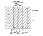
In the present embodiment, it is preferable that the opening width of the groove portion formed in the n-type GaN substrate is gradually increased from the bottom surface of the groove portion toward the opening end as in the fourth reference embodiment. As described above, since the cross-sectional shape of the
(Eighth embodiment)
FIG. 29 is a plan view for explaining a nitride-based semiconductor laser device according to the eighth embodiment of the present invention, and FIG. 30 is a cross-sectional view taken along the line 500-500 in FIG. The nitride-based semiconductor laser device according to this embodiment is different from the semiconductor laser device according to the first reference embodiment in that an n-
本実施形態においても、図1〜図4に示した第1参考形態と同様のプロセスを用いて、n型GaN基板201に、約50μmの幅W71と、約2μmの深さとを有するとともに、n型GaN基板201の上面に対して垂直な側面を有するストライプ状(細長状)の溝部201aが形成されている。ただし、前述の通り本実施形態においてはn型GaN基板201が(1−100)面を有しており、溝部201aは[11−20]方向に延びるように形成されている。
Also in this embodiment, the n-
そして、n型GaN基板上101上には、第1参考形態と同様のプロセスを用いて窒化物系半導体素子層80が形成されている。この窒化物系半導体素子層80は、第1参考形態と同様に、基板201側からn型クラッド層、活性層、p型クラッド層を有している。
A nitride-based
本実施形態で用いるGaN基板201も、第7実施形態と同様に、面内方向にc軸方向を含んでいる。このため、面内の軸方向がa軸だけの(0001)面を有するGaN基板を用いた第1〜第6参考形態に比べ、面内の軸方向としてc軸方向を含む(1−100)面を有するGaN基板を用いた本実施形態の方が、AlGaN層に加わる歪みや応力が大きくなる。このため本実施形態に係る窒化物系半導体レーザ素子も、第1〜第6参考形態に係る窒化物系半導体レーザ素子に比べ、AlGaN層にクラックが発生しやすく、その結果窒化物系半導体素子層80にクラックが発生し易い。
The
そこで、本願にあっては基板101に設ける溝部101aを[11−200]方向に延びるように設けている。
Therefore, in the present application, the
即ち、[11−20]方向はa軸方向に相当するので、(1−100)面のGaN基板を用いた本実施形態にあっては、[11−20]方向と交差する方向よりも、[0001]方向と交差する方向にクラックが発生し易い。従って、本実施形態のように[0001]方向と交差する[11−20]軸方向に沿って溝部101aを設けることにより、[0001]方向と交差する方向に発生するクラックの伝搬を効果的に抑制することができる。このように、本実施形態においては多数のクラックが発生する方向のクラックの伝搬を抑制するようにしたので、より大きな効果が得られる。
That is, since the [11-20] direction corresponds to the a-axis direction, in the present embodiment using the (1-100) plane GaN substrate, rather than the direction intersecting the [11-20] direction, Cracks are likely to occur in the direction crossing the [0001] direction. Therefore, by providing the
また、本実施形態においては、第4参考形態のように、n型GaN基板に形成する溝部の開口幅を、溝部の底面から開口端に向かって徐々に大きくすることが好ましい。このように溝部201aの断面形状がメサ形状であることにより、n型GaN基板201上にAlGaN層を含む窒化物半導体素子層80を形成する際に、AlGaN層の構成材料の一部であるGaが溝部201aの傾斜した側面側へ移動しやすくなると考えられる。このため、溝部201aの側面上に形成されるAlGaN層のAl組成比が、n型GaN基板201の領域201b上に形成されるAlGaN層のAl組成比よりも低くなる。具体的には、AlGaN層としてAl組成比が約7%の層を形成する場合、n型GaN基板201の領域201b上に形成されるAlGaN層のAl組成比が約7%であるのに対して、溝部201aの側面上に形成されるAlGaN層のAl組成比が約0.7%となる。この場合、溝部201aの側面上に位置するAlGaN層のAl組成比が低い部分の格子定数がn型GaN基板201の格子定数に近づくので、溝部201aの側面上に位置するAlGaN層のAl組成比が低い部分において、n型GaN基板201とAlGaN層との間の格子定数差が小さくなる。このため、n型GaN基板201と、窒化物半導体素子層80中のAlGaN層との間の格子定数差に起因してAlGaN層に歪みが生じたとしても、その歪みが溝部201aの側面上に位置するAlGaN層のAl組成比が低い部分において緩和されるので、AlGaN層に生じる歪みが小さくなる。これにより、AlGaN層に発生するクラックの量が増大するのが抑制されるとともに、AlGaN層を含む窒化物系半導体素子層80に発生するクラックの量が増大するのも抑制される。
In the present embodiment, it is preferable that the opening width of the groove portion formed in the n-type GaN substrate is gradually increased from the bottom surface of the groove portion toward the opening end as in the fourth reference embodiment. As described above, since the cross-sectional shape of the
また、上記第1〜第8の実施形態および参考形態では、(0001)面、(1−100面)および(11−20)面の表面を有するGaN基板を用いたが、これらの面から約1.0°以下の範囲内でオフしている窒化物系半導体基板を用いてもよい。 Further, in the embodiment and reference embodiment of the first to eighth, (0001) plane, GaN is used a substrate having a surface of (1-100 plane) and (11-20) plane, approximately from these planes A nitride-based semiconductor substrate turned off within a range of 1.0 ° or less may be used.
また、上記第1〜第8の実施形態および参考形態では、MQW構造の活性層を用いたが、本発明はこれに限らず、量子効果を有しない大きな厚みを有する単層または単一量子井戸構造の活性層であっても同様の効果を得ることができる。 Further, in the embodiment and reference embodiment of the first to eighth has used an active layer of the MQW structure, the present invention is not limited to this, a single layer or a single quantum well having a large thickness having no quantum effect A similar effect can be obtained even with an active layer having a structure.
また、上記第4参考形態および第7,8実施形態では、n型GaN基板に形成されるメサ形状の断面形状を有する溝部の底面と側面とがなす角度α(図18参照)を、約40°にしたが、本発明はこれに限らず、溝部の底面と側面とがなす角度αが、約15°以上であればよい。なお、溝部の側面の傾斜が緩やかな方が、溝部の側面上に形成される窒化物系半導体層(AlGaN層)のAl組成比を、溝部以外の領域上に形成される窒化物系半導体層(AlGaN層)のAl組成比に比べてより低くすることができる。 In the fourth reference embodiment and the seventh and eighth embodiments, the angle α (see FIG. 18) formed by the bottom surface and the side surface of the groove having a mesa-shaped cross-sectional shape formed on the n-type GaN substrate is about 40. However, the present invention is not limited to this, and the angle α formed between the bottom surface and the side surface of the groove may be about 15 ° or more. Note that the nitride composition semiconductor layer formed on the region other than the groove portion has the Al composition ratio of the nitride semiconductor layer (AlGaN layer) formed on the side surface of the groove portion when the inclination of the side surface of the groove portion is gentler. It can be made lower than the Al composition ratio of (AlGaN layer).
また、上記第4参考形態および第7,8実施形態では、溝の断面形状を(0001)面に関してほぼ面対称になるように構成したが、非対称になるように構成しても良い。即ち、図18において、溝部51aの底面と側面とがなす角度αを左右で異なる角度としてもよい。
In the fourth reference embodiment and the seventh and eighth embodiments, the cross-sectional shape of the groove is configured to be substantially plane-symmetric with respect to the (0001) plane, but may be configured to be asymmetric. That is, in FIG. 18, the angle α formed by the bottom surface and the side surface of the
また、上記第7,8実施形態において、[0001]方向と垂直な方向に延びる溝に加えて、[0001]方向に延びる溝をさらに形成し、格子状の溝としても良い。 In the seventh and eighth embodiments, in addition to the groove extending in the direction perpendicular to the [0001] direction, a groove extending in the [0001] direction may be further formed to form a lattice-like groove.
また、溝部の深さはAlGaNから構成されるn型層の厚みあるいはAlGaNから構成されるp型層の厚みより大きい値であることが好ましく、0.5μm〜30μmの範囲が好ましい。 Further, the depth of the groove is preferably larger than the thickness of the n-type layer made of AlGaN or the thickness of the p-type layer made of AlGaN, and preferably in the range of 0.5 μm to 30 μm.
また、溝部の幅はAlGaNから構成されるn型層の厚みあるいはAlGaNから構成されるp型層の厚みより大きい値であることが好ましく、5μm〜400μmの範囲が好ましい。 The width of the groove is preferably larger than the thickness of the n-type layer made of AlGaN or the thickness of the p-type layer made of AlGaN, and preferably in the range of 5 μm to 400 μm.
また、発光部分に対応する領域の幅は、10μm〜400μmの範囲が好ましい。 The width of the region corresponding to the light emitting portion is preferably in the range of 10 μm to 400 μm.
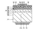
1、21、41、51、71、81、91、101、201 n型GaN基板(窒化物系半導体基板)
1a、21a、41a、41b、51a、71a、81a、91a、101a、201a 溝部
1b、21b、41c、51b、71b、81b、91b、101b、201b 領域(第1領域)
3、23、53 n型クラッド層(窒化物系半導体層)
10、30、40、60、70、80 窒化物系半導体素子層
1, 21, 41, 51, 71, 81, 91, 101, 201 n-type GaN substrate (nitride-based semiconductor substrate)
1a, 21a, 41a, 41b, 51a, 71a, 81a, 91a, 101a,
3, 23, 53 n-type cladding layer (nitride-based semiconductor layer)
10, 30, 40, 60, 70, 80 Nitride-based semiconductor element layer
Claims (12)
前記窒化物系半導体基板の前記第1領域および前記溝部上に、AlとGaとNとを含有する層を含む前記窒化物系半導体層を形成する工程とを備え、
前記窒化物系半導体基板の前記窒化物系半導体層の形成される面は(H,K,−H−K,0)面であり、
前記第1の方向は[K,−H,H−K,0]方向である、窒化物系半導体発光素子の製造方法(HとKは整数であり、HとKの少なくとも一方は0ではない)。 A predetermined region of the second region other than the first region of the nitride-based semiconductor substrate corresponding to the light-emitting portion of the nitride-based semiconductor layer formed on the nitride-based semiconductor substrate made of a GaN substrate is selectively selected to a predetermined depth. Forming an elongated groove extending in the first direction in the nitride-based semiconductor substrate,
Forming the nitride semiconductor layer including a layer containing Al, Ga and N on the first region and the groove of the nitride semiconductor substrate,
Surface formed of the nitride-based semiconductor layer of the nitride-based semiconductor substrate is (H, K, -H-K , 0) plane,
The first direction is a [K, -H, HK, 0] direction, a method for manufacturing a nitride semiconductor light emitting device (H and K are integers, and at least one of H and K is not 0) ).
前記窒化物系半導体基板の前記第1領域の上面上と、前記溝部の底面および側面上とに前記窒化物系半導体層を形成する工程を含み、
前記溝部の側面上に形成される前記窒化物系半導体層のAl組成比は、前記第1領域の上面上に形成される前記窒化物系半導体層のAl組成比よりも低い、請求項1に記載の窒化物系半導体発光素子の製造方法。 Forming the nitride-based semiconductor layer on the nitride-based semiconductor substrate,
The includes a nitride on the upper surface of the first region of the semiconductor substrate, the step of forming the nitride-based semiconductor layer and on the bottom and side surfaces of the groove,
Al composition ratio of the nitride-based semiconductor layer formed on the side surfaces of the groove is lower than the Al composition ratio of the nitride-based semiconductor layer formed on the upper surface of the first region, to claim 1 The manufacturing method of the nitride type semiconductor light-emitting device of description.
前記溝部の開口幅が、前記溝部の底面から開口端に向かって徐々に大きくなるように形成する工程を含む、請求項1または2に記載の窒化物系半導体発光素子の製造方法。 Forming the groove in the nitride-based semiconductor substrate,
3. The method for manufacturing a nitride-based semiconductor light-emitting element according to claim 1, comprising a step of forming an opening width of the groove portion so as to gradually increase from a bottom surface of the groove portion toward an opening end.
前記窒化物系半導体基板の前記第1領域の上面上、前記溝部の底面および側面上に前記窒化物系半導体層を形成する工程を含み、
前記溝部の側面上に形成される前記窒化物系半導体層の厚みは、前記第1領域の上面上に形成される前記窒化物系半導体層の厚みよりも小さい、請求項1に記載の窒化物系半導体発光素子の製造方法。 Forming the nitride-based semiconductor layer on the nitride-based semiconductor substrate,
Forming the nitride-based semiconductor layer on the top surface of the first region of the nitride-based semiconductor substrate, on the bottom surface and the side surface of the groove,
When the thickness of the nitride-based semiconductor layer formed on the side surfaces of the groove is smaller than the thickness of the nitride-based semiconductor layer formed on the upper surface of the first region, the nitride according to claim 1 For manufacturing a semiconductor light emitting device.
前記溝部の側面が、前記窒化物系半導体基板の表面に対して実質的に垂直になるように形成する工程を含む、請求項4に記載の窒化物系半導体発光素子の製造方法。 Forming the groove in the nitride-based semiconductor substrate,
The method for manufacturing a nitride-based semiconductor light-emitting element according to claim 4 , comprising a step of forming a side surface of the groove portion so as to be substantially perpendicular to a surface of the nitride-based semiconductor substrate.
前記溝部の開口幅が、前記溝部の底面から開口端に向かって徐々に小さくなるように形成する工程を含む、請求項4に記載の窒化物系半導体発光素子の製造方法。 Forming the groove in the nitride-based semiconductor substrate,
5. The method for manufacturing a nitride-based semiconductor light-emitting element according to claim 4 , comprising a step of forming the opening width of the groove portion so as to gradually decrease from the bottom surface of the groove portion toward the opening end.
前記窒化物系半導体基板に、前記第1領域を囲むように、前記第1の方向および前記第1の方向と交差する第2の方向に延びる細長状の前記溝部を格子状に形成する工程を含む、請求項1〜6のいずれか1項に記載の窒化物系半導体発光素子の製造方法。 Forming the groove in the nitride-based semiconductor substrate,
Forming in the lattice form the elongated grooves extending in the first direction and in a second direction intersecting the first direction so as to surround the first region in the nitride-based semiconductor substrate; The manufacturing method of the nitride type semiconductor light-emitting device of any one of Claims 1-6 containing.
前記第1の方向は[11−20]方向である、請求項1〜7記載の窒化物系半導体発光素子の製造方法。 The surface of the nitride-based semiconductor substrate has a (1-100) plane,
The first direction is a [11-20] direction, claim 1-7 production method for a nitride semiconductor light emitting device according.
前記窒化物系半導体基板の前記第1領域の上面および前記段差部の側面上に形成されるとともに、AlとGaとNとを含有する層を含む窒化物系半導体層とを備え、
前記窒化物系半導体基板の前記窒化物系半導体層の形成される面は(H,K,−H−K,0)面であり、
前記第1の方向は[K,−H,H−K,0]方向である、窒化物系半導体発光素子(HとKは整数であり、HとKの少なくとも一方は0ではない)。 A GaN substrate including a first region corresponding to the light emitting portion and a second region having a predetermined height and disposed adjacent to the first region via a stepped portion extending in the first direction A nitride-based semiconductor substrate,
A nitride-based semiconductor layer including a layer containing Al, Ga, and N, and formed on an upper surface of the first region of the nitride-based semiconductor substrate and a side surface of the stepped portion;
Surface formed of the nitride-based semiconductor layer of the nitride-based semiconductor substrate is (H, K, -H-K , 0) plane,
The nitride semiconductor light emitting device in which the first direction is a [K, -H, HK, 0] direction (H and K are integers, and at least one of H and K is not 0).
前記第1の方向は[11−20]方向である、請求項9〜11のいずれか1項に記載の窒化物系半導体発光素子。
The surface of the nitride-based semiconductor substrate has a (1-100) plane,
The nitride-based semiconductor light-emitting element according to any one of claims 9 to 11 , wherein the first direction is a [11-20] direction.
Priority Applications (4)
| Application Number | Priority Date | Filing Date | Title |
|---|---|---|---|
| JP2006078726A JP4928811B2 (en) | 2005-03-24 | 2006-03-22 | Nitride-based semiconductor light-emitting device manufacturing method and nitride-based semiconductor light-emitting device |
| US11/523,531 US20070221932A1 (en) | 2006-03-22 | 2006-09-20 | Method of fabricating nitride-based semiconductor light-emitting device and nitride-based semiconductor light-emitting device |
| CNA2006101543585A CN101043121A (en) | 2006-03-22 | 2006-09-22 | Method of fabricating nitride-based semiconductor light-emitting device and nitride-based semiconductor light-emitting device |
| US12/576,813 US8519416B2 (en) | 2006-03-22 | 2009-10-09 | Method of fabricating nitride-based semiconductor light-emitting device and nitride-based semiconductor light-emitting device |
Applications Claiming Priority (3)
| Application Number | Priority Date | Filing Date | Title |
|---|---|---|---|
| JP2005086669 | 2005-03-24 | ||
| JP2005086669 | 2005-03-24 | ||
| JP2006078726A JP4928811B2 (en) | 2005-03-24 | 2006-03-22 | Nitride-based semiconductor light-emitting device manufacturing method and nitride-based semiconductor light-emitting device |
Related Child Applications (1)
| Application Number | Title | Priority Date | Filing Date |
|---|---|---|---|
| JP2010100715A Division JP5580655B2 (en) | 2005-03-24 | 2010-04-26 | Nitride-based semiconductor light-emitting device manufacturing method and nitride-based semiconductor light-emitting device |
Publications (3)
| Publication Number | Publication Date |
|---|---|
| JP2006303471A JP2006303471A (en) | 2006-11-02 |
| JP2006303471A5 JP2006303471A5 (en) | 2007-03-01 |
| JP4928811B2 true JP4928811B2 (en) | 2012-05-09 |
Family
ID=37471333
Family Applications (1)
| Application Number | Title | Priority Date | Filing Date |
|---|---|---|---|
| JP2006078726A Expired - Fee Related JP4928811B2 (en) | 2005-03-24 | 2006-03-22 | Nitride-based semiconductor light-emitting device manufacturing method and nitride-based semiconductor light-emitting device |
Country Status (1)
| Country | Link |
|---|---|
| JP (1) | JP4928811B2 (en) |
Families Citing this family (6)
| Publication number | Priority date | Publication date | Assignee | Title |
|---|---|---|---|---|
| DE102008018038A1 (en) * | 2008-02-22 | 2009-08-27 | Osram Opto Semiconductors Gmbh | Optoelectronic semiconductor body and method for producing an optoelectronic semiconductor body |
| JP2009283912A (en) | 2008-04-25 | 2009-12-03 | Sanyo Electric Co Ltd | Nitride-based semiconductor device and method of manufacturing the same |
| JP5004989B2 (en) | 2009-03-27 | 2012-08-22 | シャープ株式会社 | Nitride semiconductor light emitting device, method for manufacturing the same, and semiconductor optical device |
| JP4927121B2 (en) | 2009-05-29 | 2012-05-09 | シャープ株式会社 | Nitride semiconductor wafer, nitride semiconductor device, and method of manufacturing nitride semiconductor device |
| JP5261313B2 (en) * | 2009-07-31 | 2013-08-14 | シャープ株式会社 | Nitride semiconductor wafer, nitride semiconductor device, and method of manufacturing nitride semiconductor device |
| JP5627871B2 (en) * | 2009-10-30 | 2014-11-19 | フューチャー ライト リミテッド ライアビリティ カンパニー | Semiconductor device and manufacturing method thereof |
Family Cites Families (6)
| Publication number | Priority date | Publication date | Assignee | Title |
|---|---|---|---|---|
| JP3206555B2 (en) * | 1998-08-13 | 2001-09-10 | 日本電気株式会社 | Gallium nitride based semiconductor light emitting device and method of manufacturing the same |
| JP2003017808A (en) * | 2001-07-04 | 2003-01-17 | Sony Corp | Gallium nitride based semiconductor light emitting device |
| JP2003179311A (en) * | 2001-12-12 | 2003-06-27 | Sony Corp | GaN-based semiconductor laser device and method of manufacturing the same |
| JP4056481B2 (en) * | 2003-02-07 | 2008-03-05 | 三洋電機株式会社 | Semiconductor device and manufacturing method thereof |
| JP3913194B2 (en) * | 2003-05-30 | 2007-05-09 | シャープ株式会社 | Nitride semiconductor light emitting device |
| JP4540347B2 (en) * | 2004-01-05 | 2010-09-08 | シャープ株式会社 | Nitride semiconductor laser device and manufacturing method thereof |
-
2006
- 2006-03-22 JP JP2006078726A patent/JP4928811B2/en not_active Expired - Fee Related
Also Published As
| Publication number | Publication date |
|---|---|
| JP2006303471A (en) | 2006-11-02 |
Similar Documents
| Publication | Publication Date | Title |
|---|---|---|
| JP5041902B2 (en) | Semiconductor laser element | |
| AU771942B2 (en) | Nitride semiconductor device and manufacturing method thereof | |
| JP4928874B2 (en) | Nitride-based semiconductor light-emitting device manufacturing method and nitride-based semiconductor light-emitting device | |
| US8519416B2 (en) | Method of fabricating nitride-based semiconductor light-emitting device and nitride-based semiconductor light-emitting device | |
| JP5627871B2 (en) | Semiconductor device and manufacturing method thereof | |
| JP4304750B2 (en) | Nitride semiconductor growth method and nitride semiconductor device | |
| JP2007080896A (en) | Semiconductor element | |
| WO1997011518A1 (en) | Semiconductor material, method of producing the semiconductor material, and semiconductor device | |
| JPWO2005106977A1 (en) | Nitride semiconductor device and manufacturing method thereof | |
| JP5412943B2 (en) | Nitride semiconductor light emitting device and epitaxial substrate | |
| JP2011077326A (en) | Semiconductor laser integrated element and method for manufacturing the same | |
| JP4928811B2 (en) | Nitride-based semiconductor light-emitting device manufacturing method and nitride-based semiconductor light-emitting device | |
| JP4608731B2 (en) | Manufacturing method of semiconductor laser | |
| JP4760821B2 (en) | Manufacturing method of semiconductor device | |
| JP2004165550A (en) | Nitride semiconductor device | |
| JP2008211261A (en) | Nitride semiconductor light emitting device | |
| JP2008177438A (en) | Nitride semiconductor light emitting device | |
| JP5245030B2 (en) | Nitride-based semiconductor laser device and manufacturing method thereof | |
| JP5580655B2 (en) | Nitride-based semiconductor light-emitting device manufacturing method and nitride-based semiconductor light-emitting device | |
| JP4623799B2 (en) | Semiconductor light emitting device manufacturing method and semiconductor laser | |
| JP3438675B2 (en) | Method for growing nitride semiconductor | |
| JP2009088270A (en) | Semiconductor element manufacturing method | |
| JP2009038327A (en) | Semiconductor device manufacturing method and semiconductor device | |
| JP4363415B2 (en) | Crystal film, crystal substrate and semiconductor device | |
| JP2012212920A (en) | Nitride semiconductor laser element |
Legal Events
| Date | Code | Title | Description |
|---|---|---|---|
| A521 | Request for written amendment filed |
Free format text: JAPANESE INTERMEDIATE CODE: A523 Effective date: 20070112 |
|
| A621 | Written request for application examination |
Free format text: JAPANESE INTERMEDIATE CODE: A621 Effective date: 20070112 |
|
| A131 | Notification of reasons for refusal |
Free format text: JAPANESE INTERMEDIATE CODE: A131 Effective date: 20100223 |
|
| A977 | Report on retrieval |
Free format text: JAPANESE INTERMEDIATE CODE: A971007 Effective date: 20100223 |
|
| RD02 | Notification of acceptance of power of attorney |
Free format text: JAPANESE INTERMEDIATE CODE: A7422 Effective date: 20100302 |
|
| A521 | Request for written amendment filed |
Free format text: JAPANESE INTERMEDIATE CODE: A523 Effective date: 20100426 |
|
| A131 | Notification of reasons for refusal |
Free format text: JAPANESE INTERMEDIATE CODE: A131 Effective date: 20110125 |
|
| RD04 | Notification of resignation of power of attorney |
Free format text: JAPANESE INTERMEDIATE CODE: A7424 Effective date: 20111020 |
|
| TRDD | Decision of grant or rejection written | ||
| A01 | Written decision to grant a patent or to grant a registration (utility model) |
Free format text: JAPANESE INTERMEDIATE CODE: A01 Effective date: 20120117 |
|
| A01 | Written decision to grant a patent or to grant a registration (utility model) |
Free format text: JAPANESE INTERMEDIATE CODE: A01 |
|
| A61 | First payment of annual fees (during grant procedure) |
Free format text: JAPANESE INTERMEDIATE CODE: A61 Effective date: 20120213 |
|
| FPAY | Renewal fee payment (event date is renewal date of database) |
Free format text: PAYMENT UNTIL: 20150217 Year of fee payment: 3 |
|
| R150 | Certificate of patent or registration of utility model |
Ref document number: 4928811 Country of ref document: JP Free format text: JAPANESE INTERMEDIATE CODE: R150 Free format text: JAPANESE INTERMEDIATE CODE: R150 |
|
| S111 | Request for change of ownership or part of ownership |
Free format text: JAPANESE INTERMEDIATE CODE: R313113 |
|
| FPAY | Renewal fee payment (event date is renewal date of database) |
Free format text: PAYMENT UNTIL: 20150217 Year of fee payment: 3 |
|
| R350 | Written notification of registration of transfer |
Free format text: JAPANESE INTERMEDIATE CODE: R350 |
|
| R250 | Receipt of annual fees |
Free format text: JAPANESE INTERMEDIATE CODE: R250 |
|
| R250 | Receipt of annual fees |
Free format text: JAPANESE INTERMEDIATE CODE: R250 |
|
| S111 | Request for change of ownership or part of ownership |
Free format text: JAPANESE INTERMEDIATE CODE: R313113 |
|
| R350 | Written notification of registration of transfer |
Free format text: JAPANESE INTERMEDIATE CODE: R350 |
|
| S111 | Request for change of ownership or part of ownership |
Free format text: JAPANESE INTERMEDIATE CODE: R313113 |
|
| R350 | Written notification of registration of transfer |
Free format text: JAPANESE INTERMEDIATE CODE: R350 |
|
| R250 | Receipt of annual fees |
Free format text: JAPANESE INTERMEDIATE CODE: R250 |
|
| R250 | Receipt of annual fees |
Free format text: JAPANESE INTERMEDIATE CODE: R250 |
|
| R250 | Receipt of annual fees |
Free format text: JAPANESE INTERMEDIATE CODE: R250 |
|
| R250 | Receipt of annual fees |
Free format text: JAPANESE INTERMEDIATE CODE: R250 |
|
| R250 | Receipt of annual fees |
Free format text: JAPANESE INTERMEDIATE CODE: R250 |
|
| R250 | Receipt of annual fees |
Free format text: JAPANESE INTERMEDIATE CODE: R250 |
|
| R250 | Receipt of annual fees |
Free format text: JAPANESE INTERMEDIATE CODE: R250 |
|
| LAPS | Cancellation because of no payment of annual fees |