JP4928748B2 - Semiconductor device and manufacturing method thereof - Google Patents
Semiconductor device and manufacturing method thereof Download PDFInfo
- Publication number
- JP4928748B2 JP4928748B2 JP2005186967A JP2005186967A JP4928748B2 JP 4928748 B2 JP4928748 B2 JP 4928748B2 JP 2005186967 A JP2005186967 A JP 2005186967A JP 2005186967 A JP2005186967 A JP 2005186967A JP 4928748 B2 JP4928748 B2 JP 4928748B2
- Authority
- JP
- Japan
- Prior art keywords
- insulating film
- electrode
- film
- opening
- capacitive
- Prior art date
- Legal status (The legal status is an assumption and is not a legal conclusion. Google has not performed a legal analysis and makes no representation as to the accuracy of the status listed.)
- Active
Links
Images


Classifications
-
- H—ELECTRICITY
- H01—ELECTRIC ELEMENTS
- H01L—SEMICONDUCTOR DEVICES NOT COVERED BY CLASS H10
- H01L28/00—Passive two-terminal components without a potential-jump or surface barrier for integrated circuits; Details thereof; Multistep manufacturing processes therefor
- H01L28/40—Capacitors
- H01L28/60—Electrodes
- H01L28/82—Electrodes with an enlarged surface, e.g. formed by texturisation
- H01L28/90—Electrodes with an enlarged surface, e.g. formed by texturisation having vertical extensions
- H01L28/91—Electrodes with an enlarged surface, e.g. formed by texturisation having vertical extensions made by depositing layers, e.g. by depositing alternating conductive and insulating layers
-
- H—ELECTRICITY
- H01—ELECTRIC ELEMENTS
- H01L—SEMICONDUCTOR DEVICES NOT COVERED BY CLASS H10
- H01L28/00—Passive two-terminal components without a potential-jump or surface barrier for integrated circuits; Details thereof; Multistep manufacturing processes therefor
- H01L28/40—Capacitors
- H01L28/60—Electrodes
- H01L28/82—Electrodes with an enlarged surface, e.g. formed by texturisation
- H01L28/86—Electrodes with an enlarged surface, e.g. formed by texturisation having horizontal extensions
- H01L28/87—Electrodes with an enlarged surface, e.g. formed by texturisation having horizontal extensions made by depositing layers, e.g. by depositing alternating conductive and insulating layers
-
- H—ELECTRICITY
- H10—SEMICONDUCTOR DEVICES; ELECTRIC SOLID-STATE DEVICES NOT OTHERWISE PROVIDED FOR
- H10B—ELECTRONIC MEMORY DEVICES
- H10B12/00—Dynamic random access memory [DRAM] devices
- H10B12/01—Manufacture or treatment
- H10B12/02—Manufacture or treatment for one transistor one-capacitor [1T-1C] memory cells
- H10B12/03—Making the capacitor or connections thereto
- H10B12/033—Making the capacitor or connections thereto the capacitor extending over the transistor
Landscapes
- Engineering & Computer Science (AREA)
- Power Engineering (AREA)
- Computer Hardware Design (AREA)
- Microelectronics & Electronic Packaging (AREA)
- Manufacturing & Machinery (AREA)
- Semiconductor Integrated Circuits (AREA)
- Inductance-Capacitance Distribution Constants And Capacitance-Resistance Oscillators (AREA)
- Internal Circuitry In Semiconductor Integrated Circuit Devices (AREA)
Description
本発明は、半導体装置、及びそれを用いた送受信装置、並びにその半導体装置の製造方法に関し、特に、半導体チップに形成された容量素子の占有面積を低減する半導体装置に適用して有効な技術に関するものである。 The present invention relates to a semiconductor device, a transmission / reception device using the same, and a method for manufacturing the semiconductor device, and more particularly, to a technique effective when applied to a semiconductor device that reduces the occupied area of a capacitor formed on a semiconductor chip. Is.
MIM(Metal Insulator Metal)構造からなる容量素子を積層構造にすることにより、容量を確保しながら容量素子の占有面積を低減する技術が開示されている(例えば、特許文献1または特許文献2参照)。
There has been disclosed a technique for reducing the occupation area of a capacitive element while securing the capacitance by forming a capacitive element having a MIM (Metal Insulator Metal) structure into a laminated structure (see, for example,
また、DRAM(Dynamic Random Access Memory)において、ポリシリコン膜からなる電極を有する容量素子を積層構造にし、かつ、容量素子の端部を持ち上げた構造が開示されている(例えば、特許文献3)。
上述した特許文献1あるいは特許文献2においては、下部電極と下部電極上に形成された第1容量絶縁膜と第1容量絶縁膜上に形成された中間電極によって第1容量素子が形成されている。そして、中間電極と中間電極上に形成された第2容量絶縁膜と第2容量絶縁膜上に形成された上部電極によって第2容量素子が形成されている。このように、第1容量素子と第2容量素子は積層されているが、このとき、中間電極は、中間電極のすべての部分で第1容量絶縁膜と直接接している。したがって、中間電極による寄生容量(層間容量)は、第1容量素子の容量と同等となる。
In
ここで、中間電極を第1容量素子および第2容量素子の電極に使用する他、信号配線や電源配線としても使用したい要求がある。しかし、上述した特許文献1あるいは特許文献2に記載された構造では、中間電極による寄生容量が第1容量素子と同等で大きなものとなるので、一般配線として使用すると信号遅延や消費電力が増加する。このため、実質的には、中間電極を一般配線として使用することが困難になるという問題がある。特に、高周波を使用した回路では、高速動作を必要とするため、配線間の寄生容量を低減しなければ、中間電極を一般配線として使用できない問題点がある。
Here, in addition to using the intermediate electrode as the electrode of the first capacitor element and the second capacitor element, there is a demand to use it as a signal wiring or a power supply wiring. However, in the structure described in
また、特許文献3には、DRAMの容量素子の電極としてポリシリコン膜を使用する場合が記載されている。ポリシリコン膜は、MIM構造の電極に使用される金属膜より抵抗値が高い。さらに、通常、ポリシリコン膜を使用した容量素子では電極間距離を、金属膜を使用した容量素子の電極間距離に比べて小さくしている。このため、寄生容量も大きくなる。このことから、ポリシリコン膜を使用した電極は、金属膜を使用した電極に比べて信号遅延および消費電力の増加が生じる。したがって、ポリシリコン膜を使用した電極を一般配線に使用することが困難となる。特許文献3には、寄生容量を低減する記載はなされておらず、示唆もされていない。
本発明の目的は、容量素子の占有面積を低減させながら、容量素子の寄生容量を低減できる技術を提供することにある。 An object of the present invention is to provide a technique capable of reducing the parasitic capacitance of a capacitive element while reducing the area occupied by the capacitive element.
本発明の前記ならびにその他の目的と新規な特徴は、本明細書の記述および添付図面から明らかになるであろう。 The above and other objects and novel features of the present invention will be apparent from the description of this specification and the accompanying drawings.
本願において開示される発明のうち、代表的なものの概要を簡単に説明すれば、次のとおりである。 Of the inventions disclosed in the present application, the outline of typical ones will be briefly described as follows.
本発明による半導体装置は、金属膜よりなる第1電極と、前記第1電極上に形成された第1容量絶縁膜と、前記第1容量絶縁膜上に形成された金属膜よりなる第2電極とを備える。そして、さらに、前記第2電極上に形成された第2容量絶縁膜と、前記第2容量絶縁膜上に形成された金属膜よりなる第3電極とを備え、前記第1電極には、前記第1容量絶縁膜と直接接していない部分がある容量素子を含むことを特徴とするものである。 A semiconductor device according to the present invention includes a first electrode made of a metal film, a first capacitor insulating film formed on the first electrode, and a second electrode made of a metal film formed on the first capacitor insulating film. With. The first electrode further includes a second capacitor insulating film formed on the second electrode and a third electrode made of a metal film formed on the second capacitor insulating film. It includes a capacitor element having a portion that is not in direct contact with the first capacitor insulating film.
また、本発明による送受信装置は、電波を送受信する送受信装置であって、金属膜よりなる第1電極と、前記第1電極上に形成された第1容量絶縁膜と、前記第1容量絶縁膜上に形成された金属膜よりなる第2電極とを備える。そして、さらに、前記第2電極上に形成された第2容量絶縁膜と、前記第2容量絶縁膜上に形成された金属膜よりなる第3電極とを備え、前記第1電極には、前記第1容量絶縁膜と直接接していない部分がある容量素子を含むことを特徴とするものである。 The transceiver device according to the present invention is a transceiver device that transmits and receives radio waves, and includes a first electrode made of a metal film, a first capacitor insulating film formed on the first electrode, and the first capacitor insulating film. And a second electrode made of a metal film formed thereon. The first electrode further includes a second capacitor insulating film formed on the second electrode and a third electrode made of a metal film formed on the second capacitor insulating film. It includes a capacitor element having a portion that is not in direct contact with the first capacitor insulating film.
また、本発明による半導体装置の製造方法は、(a)半導体基板上に第1電極を形成する工程と、(b)前記第1電極上に第1絶縁膜を形成する工程と、(c)前記第1絶縁膜に前記第1電極に達する第1開口部を形成する工程と、(d)前記第1開口部内を含む前記第1絶縁膜上に第1容量絶縁膜を形成する工程とを備える。そして、さらに、(e)前記第1開口部内を含む前記第1容量絶縁膜上に第1導体膜を形成する工程と、(f)前記第1導体膜をパターニングして第2電極を形成する工程と、(g)前記第2電極上を含む前記半導体基板上に第2絶縁膜を形成する工程と、(h)前記第2絶縁膜に前記第2電極に達する第2開口部を形成する工程とを備える。さらに、(i)前記第2開口部内を含む前記第2絶縁膜上に第2容量絶縁膜を形成する工程と、(j)前記第2開口部内を含む前記第2容量絶縁膜上に第2導体膜を形成する工程と、(k)前記第2導体膜をパターニングして第3電極を形成する工程とを備えることを特徴とするものである。 In addition, the method of manufacturing a semiconductor device according to the present invention includes (a) a step of forming a first electrode on a semiconductor substrate, (b) a step of forming a first insulating film on the first electrode, and (c). Forming a first opening reaching the first electrode in the first insulating film; and (d) forming a first capacitive insulating film on the first insulating film including the inside of the first opening. Prepare. (E) forming a first conductor film on the first capacitive insulating film including the inside of the first opening; and (f) patterning the first conductor film to form a second electrode. (G) forming a second insulating film on the semiconductor substrate including on the second electrode; and (h) forming a second opening reaching the second electrode in the second insulating film. A process. And (i) forming a second capacitor insulating film on the second insulating film including the inside of the second opening, and (j) forming a second on the second capacitor insulating film including the inside of the second opening. A step of forming a conductor film; and (k) a step of patterning the second conductor film to form a third electrode.
本願において開示される発明のうち、代表的なものによって得られる効果を簡単に説明すれば以下のとおりである。 Among the inventions disclosed in the present application, effects obtained by typical ones will be briefly described as follows.
複数の容量素子を積層するとともに容量素子を構成する電極に容量絶縁膜と直接接しない部分を設けることにより、容量素子の占有面積を低減させながら、容量素子の寄生容量を低減できる。 By stacking a plurality of capacitive elements and providing a portion not directly in contact with the capacitive insulating film on the electrode constituting the capacitive element, the parasitic capacity of the capacitive element can be reduced while reducing the area occupied by the capacitive element.
以下の実施の形態においては便宜上その必要があるときは、複数のセクションまたは実施の形態に分割して説明するが、特に明示した場合を除き、それらはお互いに無関係なものではなく、一方は他方の一部または全部の変形例、詳細、補足説明等の関係にある。 In the following embodiments, when it is necessary for the sake of convenience, the description will be divided into a plurality of sections or embodiments. However, unless otherwise specified, they are not irrelevant to each other. There are some or all of the modifications, details, supplementary explanations, and the like.
また、以下の実施の形態において、要素の数等(個数、数値、量、範囲等を含む)に言及する場合、特に明示した場合および原理的に明らかに特定の数に限定される場合等を除き、その特定の数に限定されるものではなく、特定の数以上でも以下でもよい。 Further, in the following embodiments, when referring to the number of elements (including the number, numerical value, quantity, range, etc.), especially when clearly indicated and when clearly limited to a specific number in principle, etc. Except, it is not limited to the specific number, and may be more or less than the specific number.
さらに、以下の実施の形態において、その構成要素(要素ステップ等も含む)は、特に明示した場合および原理的に明らかに必須であると考えられる場合等を除き、必ずしも必須のものではないことは言うまでもない。 Further, in the following embodiments, the constituent elements (including element steps and the like) are not necessarily indispensable unless otherwise specified and apparently essential in principle. Needless to say.
同様に、以下の実施の形態において、構成要素等の形状、位置関係等に言及するときは、特に明示した場合および原理的に明らかにそうではないと考えられる場合等を除き、実質的にその形状等に近似または類似するもの等を含むものとする。このことは、上記数値および範囲についても同様である。 Similarly, in the following embodiments, when referring to the shape, positional relationship, etc., of components, etc., unless otherwise specified, and in principle, it is considered that this is not clearly the case, it is substantially the same. Including those that are approximate or similar to the shape. The same applies to the above numerical values and ranges.
本発明の実施の形態を図面に基づいて詳細に説明する。なお、実施の形態を説明するための全図において、同一の部材には原則として同一の符号を付し、その繰り返しの説明は省略する。 Embodiments of the present invention will be described in detail with reference to the drawings. Note that components having the same function are denoted by the same reference symbols throughout the drawings for describing the embodiment, and the repetitive description thereof will be omitted.
(実施の形態1)
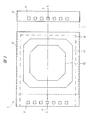
図1は、本実施の形態1における半導体装置の一部を示した断面図である。図1に示すように、シリコン単結晶よりなる半導体基板1には、nチャネル型MISFET(Metal Insulator Semiconductor Field Effect Transistor)2およびpチャネル型MISFET3が形成されている。また、nチャネル型MISFET2およびpチャネル型MISFET3の形成領域とは別の領域には、MIM構造を有する容量素子4が形成されている。すなわち、半導体基板1上には、MISFETや容量素子などが形成されている。以下の図面においては、半導体基板1に形成されているMISFETの図示は省略し、層間絶縁膜上に形成された容量素子だけを図示するものとする。
(Embodiment 1)
FIG. 1 is a cross-sectional view showing a part of the semiconductor device according to the first embodiment. As shown in FIG. 1, an n-channel MISFET (Metal Insulator Semiconductor Field Effect Transistor) 2 and a p-
図1に示す容量素子4を上部から見た平面図を図2に示す。図2において、容量素子4には、下部電極(第1電極)10が形成されており、この下部電極10上には絶縁膜(図示せず)を介して中間電極(第2電極)11が形成されている。この下部電極10と中間電極11が平面上で重なり合う領域に容量素子(第1容量素子)C1が形成されている。さらに、中間電極11上には、絶縁膜(図示せず)を介して上部電極(第3電極)12および配線13が形成されている。これにより、中間電極11と上部電極12が平面上で重なり合う領域に容量素子(第2容量素子)C2が形成される。そして、下部電極10と上部電極12とはプラグ14を介して電気的に接続されており、また、中間電極11は、プラグ15を介して配線13に接続されている。このように、容量素子4は、容量素子C1と容量素子C2とを基板の厚さ方向に積層した構造を有している。したがって、本実施の形態1では、容量素子C1と容量素子C2とを積層構造にせずに平面的に配置する場合に比べて、容量素子の半導体基板に占める占有面積を低減することができる。
A plan view of the
図3は、図2のA−A線で切断した断面図を示している。図3に示すように、半導体基板上には、層間絶縁膜として絶縁膜16が形成されており、この絶縁膜16上には、下部電極10が形成されている。下部電極10は、例えば、窒化チタン膜17a、アルミニウム膜17bおよび窒化チタン膜17cの積層膜から形成されている。なお、下部電極は、上述した積層膜に限らず、例えば、タングステン膜、あるいはアルミニウム膜をチタン膜やタングステン膜などの高融点金属で積層した膜から構成してもよい。
FIG. 3 shows a cross-sectional view taken along line AA in FIG. As shown in FIG. 3, an insulating
下部電極10上を含む絶縁膜16上には、絶縁膜(第1絶縁膜)19が形成されている。この絶縁膜19には、開口部(溝)19aが形成されており、開口部19aの底部において下部電極10が露出するようになっている。このように、下部電極10の一部領域上には開口部19aが形成されており、その他の領域は、絶縁膜19が形成されている。したがって、下部電極10に開口部19aを設けることにより、下部電極10上に段差が形成されている。
An insulating film (first insulating film) 19 is formed on the insulating
開口部19aの内部を含む絶縁膜19上には、容量絶縁膜(第1容量絶縁膜)18が形成されている。この容量絶縁膜18は、例えば、酸化シリコン膜、窒化シリコン膜、酸化アルミニウム膜あるいは、タンタルやハフニウムなどの酸化物を含む膜から形成されている。容量絶縁膜18として、酸化アルミニウム膜、タンタルやハフニウムなどの酸化物を含む膜から構成することにより、容量絶縁膜18を高誘電率の膜とすることができ、容量密度の向上が可能となる。一方、容量絶縁膜18を酸化シリコン膜や窒化シリコン膜から構成することにより、容量素子の耐圧向上を図ることができる。また、容量絶縁膜18を酸化シリコン膜や窒化シリコン膜から構成することで、誘電率の温度依存性や周波数依存性を少なくすることができる。つまり、容量絶縁膜18の温度特性および周波数特性を改善することができる。
A capacitor insulating film (first capacitor insulating film) 18 is formed on the insulating
容量絶縁膜18は、開口部19aの内部を含む絶縁膜19上に形成されているので、開口部19aの底部に形成されている容量絶縁膜18は、下部電極10と直接接していることになる。一方、開口部19a以外の絶縁膜19上に形成されている容量絶縁膜18は、下部電極10と直接接していない。すなわち、下部電極10と容量絶縁膜18の間には絶縁膜19が形成されている。このように、下部電極10と容量絶縁膜18は、直接接している部分と直接接していない部分があり、この点が本実施の形態1の特徴の一つである。
Since the
次に、容量絶縁膜18上には、中間電極11が形成されている。中間電極11は、例えば窒化チタン膜20a、アルミニウム膜20bおよび窒化チタン膜20cの積層膜から形成されるが、前述した下部電極10と同様に他の材料を用いてもよい。中間電極11は、開口部19a内を含む容量絶縁膜18上に形成されているため、中間電極11には段差が形成されている。この中間電極11、容量絶縁膜18および下部電極10により、一つの容量素子C1(図2参照)が形成される。このとき、開口部19a内において、容量素子C1が形成されている。すなわち、開口部19a内においては、下部電極10上に直接接するように容量絶縁膜18が形成されており、この容量絶縁膜18上に直接、中間電極11が形成されているので、下部電極10と中間電極11との距離が短くなり容量が大きくなる。したがって、容量が大きくなる開口部19a内が容量素子C1として支配的に機能する。一方、開口部19a以外の領域では、下部電極10と容量絶縁膜18の間に絶縁膜19が形成されている。このため、下部電極10と中間電極11との距離は、開口部19a内に比べて大きくなり、容量に対する寄与は少なくなる。
Next, the
従来、上部に中間電極がある下部電極の領域において、下部電極は容量絶縁膜と直接接していた。しかし、この場合、容量素子が形成されている領域以外においても下部電極と中間電極との距離が容量素子形成領域と同様に近くなっていた。このため、中間電極を容量素子の電極以外に使用する場合に寄生容量が容量素子の容量と同等となって大きくなる問題点があった。すなわち、中間電極の寄生容量が大きくなって、中間電極を信号配線や電源配線などの一般配線としても使用するには、信号遅延や消費電力の増加が無視できない事態になっていた。 Conventionally, the lower electrode is in direct contact with the capacitive insulating film in the region of the lower electrode having the upper intermediate electrode. However, in this case, the distance between the lower electrode and the intermediate electrode is close to that in the capacitive element forming region, except in the region where the capacitive element is formed. For this reason, when the intermediate electrode is used other than the electrode of the capacitive element, there is a problem that the parasitic capacitance becomes equal to the capacitance of the capacitive element and becomes large. That is, the parasitic capacitance of the intermediate electrode is increased, and in order to use the intermediate electrode as a general wiring such as a signal wiring or a power supply wiring, a signal delay or an increase in power consumption cannot be ignored.
そこで、本実施の形態1では、容量素子形成領域においては、下部電極10と中間電極11との距離を近づけて容量を確保する一方、容量素子形成領域以外の領域においては、下部電極10と中間電極11の間に絶縁膜19を設けて下部電極10と中間電極11との距離を遠ざけている。つまり、容量素子形成領域において、下部電極10は、容量絶縁膜18と直接接するように構成されているが、その他の領域において、下部電極10と容量絶縁膜18の間に絶縁膜19を設けることにより、下部電極10を容量絶縁膜18と直接接しないように構成している。これにより、下部電極10が容量絶縁膜18と直接接していない領域上で、下部電極10と中間電極11との距離が大きくなるので、中間電極11を一般配線に使用したとき、下部電極10との間で生じる寄生容量を小さくすることができる。言い換えれば、下部電極10上に開口部19aによる段差を設けて、開口部19a内(容量素子形成領域)での下部電極10と中間電極11の距離よりも、開口部19aの外側の領域での下部電極10と中間電極11との距離を大きくしている。このため、中間電極11を信号配線や電源配線に使用した場合における信号遅延や消費電力の増加を抑制することができる。
Therefore, in the first embodiment, in the capacitor element formation region, the distance between the
次に、中間電極11上には、絶縁膜(第2絶縁膜)22が形成されており、この絶縁膜22には開口部22aが設けられている。この開口部22aの底部には、中間電極11が露出している。そして、開口部22aの内部を含む絶縁膜22上には、容量絶縁膜(第2容量絶縁膜)21が形成されており、容量絶縁膜21上には、窒化チタン膜23が形成されている。さらに、窒化チタン膜23上を含む絶縁膜22上には、上部電極12および配線13が形成されている。
Next, an insulating film (second insulating film) 22 is formed on the
上部電極12および配線13は、例えば、窒化チタン膜24a、アルミニウム膜24bおよび窒化チタン膜24cの積層膜から構成されている。この上部電極12、容量絶縁膜21および中間電極11により、図2に示す容量素子C2が形成されている。すなわち、本実施の形態1では、下部電極10、容量絶縁膜18および中間電極11よりなる容量素子C1上に、中間電極11、容量絶縁膜21および上部電極12よりなる容量素子C2が形成されている。つまり、本実施の形態1では、容量素子C1および容量素子C2が積層構造で形成されている。このように、容量素子C1および容量素子C2を積層構造とすることにより、半導体基板に占める容量素子の占有面積を低減することができるので、半導体チップの縮小化が図られ、低コスト化を実現できる。または、容量素子の占有面積を低減できるので、他の機能を有する素子を半導体チップ上に搭載することができる。このため、半導体チップの高機能化および高性能化を図ることができる。
The
上部電極12、容量絶縁膜21および中間電極11により、一つの容量素子C2(図2参照)が形成されるが、このとき、開口部22a内において、容量素子C2が形成されている。すなわち、開口部22a内においては、中間電極11上に直接接するように容量絶縁膜21が形成されており、この容量絶縁膜21上に直接、上部電極12が形成されているので、中間電極11と上部電極12との距離が短くなり容量が大きくなる。したがって、容量が大きくなる開口部22a内が容量素子C2として支配的に機能する。一方、開口部22a以外の領域(容量形成領域以外の領域)では、中間電極11と容量絶縁膜21の間に絶縁膜22が形成されており、中間電極11は、容量絶縁膜21と直接接していない。このため、中間電極11と上部電極12との距離は、開口部22a内に比べて大きくなり、容量に対する寄与は少なくなる。つまり、中間電極11と上部電極12との間の寄生容量を低減することができる。
The
また、図3に示すように、下部電極10と上部電極12とは、プラグ14を介して電気的に接続されている。そして、中間電極11は、プラグ15を介して配線13と電気的に接続されている。したがって、下部電極10、容量絶縁膜18および中間電極11よりなる容量素子C1と、中間電極11、容量絶縁膜21および上部電極12よりなる容量素子C2は、電気的に並列接続されている。このため、積層された容量素子C1と容量素子C2による総容量は、容量素子C1の容量と容量素子C2の容量の和となる。このことから、積層化することによって容量素子の占有面積を低減しても、トータルの総容量を確保できる。
Further, as shown in FIG. 3, the
本実施の形態1によれば、容量素子を積層構造にすることによって容量素子の占有面積を低減しつつも、積層化された容量素子を並列接続することにより、トータルの総容量を確保することができる。さらに、容量素子形成領域以外の領域では、電極間距離を容量素子形成領域に比べて大きくすることができるので、寄生容量を低減できる。このため、信号遅延や消費電力の低減を実現できるので、容量素子の電極を信号配線や電源配線として使用することができる。そして、電極を一般配線として利用できるので、半導体チップに引き回される配線も短くすることができ、その配線の寄生容量および配線抵抗を低減できる。また、電極を一般配線と共用することができるので、配線数も縮小でき、半導体チップの小型化をさらに推進することができる。また、電極を一般配線として用いることができるので、配線の設計などの設計自由度が増大する利点もある。 According to the first embodiment, the total capacity is ensured by connecting the stacked capacitive elements in parallel while reducing the occupied area of the capacitive elements by forming the capacitive elements in a stacked structure. Can do. Furthermore, in the region other than the capacitor element formation region, the inter-electrode distance can be made larger than that of the capacitor element formation region, so that the parasitic capacitance can be reduced. For this reason, since signal delay and power consumption can be reduced, the electrode of the capacitor can be used as a signal wiring or a power supply wiring. Since the electrode can be used as a general wiring, the wiring routed to the semiconductor chip can be shortened, and the parasitic capacitance and wiring resistance of the wiring can be reduced. In addition, since the electrode can be shared with the general wiring, the number of wirings can be reduced, and the miniaturization of the semiconductor chip can be further promoted. In addition, since the electrode can be used as a general wiring, there is an advantage that the degree of freedom of design such as wiring design is increased.
なお、本実施の形態1によれば、開口部19a内に容量素子C1が形成され、開口部19aより小さい開口部22a内に容量素子C2が形成される。このため、容量絶縁膜18と下部電極10の接触面積は、容量絶縁膜21と中間電極11の接触面積よりも大きくなっている。
According to the first embodiment, the capacitive element C1 is formed in the
次に、具体的に中間電極を一般配線として使用する場合の寄生容量(層間容量)を本発明者らが検討した構造の容量素子と本実施の形態1における構造の容量素子で比較した結果を示す。 Next, the parasitic capacitance (interlayer capacitance) when the intermediate electrode is specifically used as a general wiring is compared between the capacitive element having the structure studied by the present inventors and the capacitive element having the structure in the first embodiment. Show.
図3に示すように、本実施の形態1では、容量素子形成領域以外の領域の下部電極10と中間電極11との距離はd1であり、中間電極11と上部電極12との距離はd2となっている。すなわち、容量素子形成領域以外の領域の電極間距離は、容量素子形成領域(開口部19a、22a内の領域)の電極間距離に比べて大きくなっている。
As shown in FIG. 3, in the first embodiment, the distance between the
一方、本発明者らが検討した構造を図4に示す。図4に示すように、本発明者らが検討した構造では、下部電極100、容量絶縁膜101、中間電極102、容量絶縁膜103および上部電極104が積層構造をしている。そして、下部電極100と中間電極102との間の距離は、容量形成領域も容量形成領域以外の領域もd3となっている。同様に、中間電極102と上部電極104との間の距離は、容量形成領域も容量形成領域以外の領域もd4となっている。
On the other hand, the structure examined by the present inventors is shown in FIG. As shown in FIG. 4, in the structure investigated by the present inventors, the
中間電極と下部電極との間の寄生容量の比(本実施の形態1の寄生容量/本発明者らが検討した構造の寄生容量)を求めると、(ε1/d1)/(ε2/d3)=(ε1・d3)/(ε2・d1)となる。同様に、中間電極と上部電極との間の寄生容量の比は、(ε1/d2)/(ε2/d4)=(ε1・d4)/(ε2・d2)となる。 When the ratio of the parasitic capacitance between the intermediate electrode and the lower electrode (parasitic capacitance of the first embodiment / parasitic capacitance of the structure investigated by the present inventors) is obtained, (ε1 / d1) / (ε2 / d3) = (Ε1 · d3) / (ε2 · d1). Similarly, the ratio of the parasitic capacitance between the intermediate electrode and the upper electrode is (ε1 / d2) / (ε2 / d4) = (ε1 · d4) / (ε2 · d2).
ここで、本実施の形態1の構造において、容量絶縁膜18および容量絶縁膜21が酸化シリコン膜から形成されているとすると、ε1=4.2となる。そして、d1およびd2の大きさを500nmとする。また、本発明者らが検討した構造において、容量絶縁膜101および容量絶縁膜103が窒化シリコン膜から形成されているとすると、ε2=7となる。そして、d3およびd4の大きさを50nmとする。
Here, in the structure of the first embodiment, assuming that the
この条件で本実施の形態1における寄生容量の低減を計算すると以下に示す結果が得られた。すなわち、本発明者らが検討した構造の寄生容量を100とした場合、本実施の形態1における寄生容量は6となり、1桁以上、寄生容量を低減することができる。 When the reduction of the parasitic capacitance in the first embodiment was calculated under this condition, the following results were obtained. That is, when the parasitic capacitance of the structure studied by the present inventors is 100, the parasitic capacitance in the first embodiment is 6, and the parasitic capacitance can be reduced by one digit or more.
中間配線を信号配線や電源配線などの一般配線に使用する場合、配線による信号遅延は、配線抵抗×寄生容量に比例し、消費電極も寄生容量に比例する。寄生容量は、一般に同層の隣接する配線との間の寄生容量と、上下層間にある配線との寄生容量との和になる。ここで、同層の隣接する配線間の距離が離れていて、この寄生容量が無視できる場合、寄生容量は、上下層間にある配線との寄生容量になる。この条件では、上述したように寄生容量を1桁以上低減することができるので、中間電極を配線に用いた場合の信号遅延および消費電力は、最大1桁低減することが可能となる。すなわち、本実施の形態1によれば、本発明者らが検討した構造の中間電極を一般配線に利用する場合に比べて、大幅に寄生容量を少なくできるので、配線による信号遅延の低減および消費電力の低減を実現できる。 When intermediate wiring is used for general wiring such as signal wiring and power supply wiring, signal delay due to wiring is proportional to wiring resistance × parasitic capacitance, and the consumption electrode is also proportional to parasitic capacitance. The parasitic capacitance is generally the sum of the parasitic capacitance between adjacent wirings in the same layer and the parasitic capacitance between wirings in the upper and lower layers. Here, when the distance between adjacent wirings in the same layer is large and the parasitic capacitance can be ignored, the parasitic capacitance becomes a parasitic capacitance with the wiring in the upper and lower layers. Under this condition, the parasitic capacitance can be reduced by one digit or more as described above, so that the signal delay and power consumption when the intermediate electrode is used for the wiring can be reduced by one digit at the maximum. That is, according to the first embodiment, the parasitic capacitance can be greatly reduced as compared with the case where the intermediate electrode having the structure studied by the present inventors is used for the general wiring. Reduction of power can be realized.
次に、本実施の形態1における容量素子の製造方法について、図面を参照しながら説明する。 Next, a method for manufacturing the capacitive element in the first embodiment will be described with reference to the drawings.
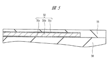
まず、図示しない半導体基板上にMISFETを形成し、このMISFETに接続する配線を形成する。その後、配線上に層間絶縁膜となる絶縁膜30を形成する。図5には、絶縁膜30を形成した後の工程が記載されている。絶縁膜30は、例えば、酸化シリコン膜から形成され、例えばCVD(Chemical Vapor Deposition)法を使用して形成することができる。
First, a MISFET is formed on a semiconductor substrate (not shown), and wiring connected to the MISFET is formed. Thereafter, an insulating
次に、絶縁膜30上に窒化チタン膜31a、アルミニウム膜31bおよび窒化チタン膜31cを順次、積層して形成する。窒化チタン膜31a、アルミニウム膜31bおよび窒化チタン膜31cは、例えば、スパッタリング法を使用して形成することができる。続いて、フォトリソグラフィ技術およびエッチング技術を使用して、窒化チタン膜31a、アルミニウム膜31bおよび窒化チタン膜31cをパターニングする。これにより、窒化チタン膜31a、アルミニウム膜31bおよび窒化チタン膜31cよりなる下部電極(第1電極)32が形成される。そして、下部電極32を含む絶縁膜30上に絶縁膜(第1絶縁膜)33を形成する。この絶縁膜33も、例えばCVD法を使用した酸化シリコン膜より形成することができる。
Next, a
続いて、図6に示すように、絶縁膜33上にレジスト膜34を塗布した後、レジスト膜34に対して露光・現像処理を施すことにより、レジスト膜34をパターニングする。パターニングは、開口部35を形成する領域にレジスト膜34が残らないようにする。次に、パターニングしたレジスト膜34をマスクにして絶縁膜33をエッチングする。これにより、絶縁膜33に開口部(第1開口部)35が形成される。この開口部35の底部には、下部電極32が露出している。
Subsequently, as shown in FIG. 6, after a resist
次に、レジスト膜34を除去した後、図7に示すように、開口部35内を含む絶縁膜33上に容量絶縁膜(第1容量絶縁膜)36を形成する。容量絶縁膜36は、例えば、CVD法を使用して形成することができ、例えば、酸化シリコン膜、窒化シリコン膜、酸化アルミニウム膜あるいは、タンタルやハフニウムなどの酸化物を含む膜から形成することができる。
Next, after removing the resist
そして、容量絶縁膜36上に窒化チタン膜37a、アルミニウム膜37bおよび窒化チタン膜37cを順次、スパッタリング法で形成する(第1導体膜)。その後、窒化チタン膜37c上にレジスト膜38を塗布し、塗布したレジスト膜38に対して露光・現像処理を施す。これにより、レジスト膜38をパターニングする。パターニングは、中間電極形成領域にレジスト膜38が残るようにする。続いて、パターニングしたレジスト膜38をマスクにしたエッチングにより、中間電極(第2電極)39を形成する。このとき、開口部35内においては、下部電極32、容量絶縁膜36および中間電極39により第1容量素子が形成される。一方、開口部35の外側の領域において、下部電極32は、容量絶縁膜36と直接接しておらず、下部電極32と中間電極39の間には、絶縁膜33が形成されている。この領域は、容量素子形成領域ではないため、下部電極32と中間電極39との間は容量素子形成領域よりも離れており、寄生容量の低減が図られている。
Then, a
次に、レジスト膜38を除去した後、図8に示すように、中間電極39上を含む絶縁膜33上に絶縁膜(第2絶縁膜)40を形成する。絶縁膜40は、例えば、CVD法を用いた酸化シリコン膜より形成することができる。続いて、絶縁膜40上にレジスト膜41を塗布した後、露光・現像処理を施すことにより、レジスト膜41をパターニングする。パターニングは、接続孔形成領域にレジスト膜41が残らないようにする。そして、パターニングしたレジスト膜41をマスクにしたエッチングにより、接続孔42および接続孔43を形成する。接続孔42は下部電極32に達しており、接続孔43は中間電極39に達している。
Next, after removing the resist
次に、レジスト膜41を除去した後、図9に示すように、接続孔42および接続孔43に導電材料を埋め込んでプラグ44およびプラグ45を形成する。プラグ44およびプラグ45は、例えば窒化チタン膜およびタングステン膜の積層膜を、接続孔42、43内を含む絶縁膜40上に形成した後、CMP(Chemical Mechanical Polishing)法を使用して絶縁膜40上に形成された積層膜を研磨することにより形成される。
Next, after removing the resist
続いて、図10に示すように、絶縁膜40上にレジスト膜46を塗布した後、露光・現像処理を施すことにより、レジスト膜46をパターニングする。パターニングは、開口部形成領域にレジスト膜46が残らないようにする。そして、パターニングしたレジスト膜46をマスクにしてエッチングすることにより、開口部(第2開口部)47を形成する。
Subsequently, as shown in FIG. 10, after applying a resist
次に、図11に示すように、開口部47内を含む絶縁膜40上に容量絶縁膜(第2容量絶縁膜)48および窒化チタン膜49を積層して形成する。そして、窒化チタン膜49上にレジスト膜50を塗布した後、露光・現像処理を施すことにより、レジスト膜50をパターニングする。続いて、パターニングしたレジスト膜50をマスクにして、容量絶縁膜48および窒化チタン膜49をエッチングする。
Next, as shown in FIG. 11, a capacitor insulating film (second capacitor insulating film) 48 and a
次に、図12に示すように、パターニングした窒化チタン膜49を含む絶縁膜40上に、窒化チタン膜51a、アルミニウム膜51bおよび窒化チタン膜51cを順次、スパッタリング法で形成する(第2導体膜)。その後、フォトリソグラフィ技術およびエッチング技術を使用して、これらの膜をパターニングすることにより、窒化チタン膜51a、アルミニウム膜51bおよび窒化チタン膜51cよりなる上部電極(第3電極)52を形成することができる。開口部47内には、中間電極39、容量絶縁膜48および上部電極52よりなる第2容量素子が形成される。一方、開口部47の外側の領域においては、中間電極39と上部電極52との間に絶縁膜40が形成されている。このため、中間電極39と上部電極52との距離が容量形成領域より大きくなっているので、中間電極39の寄生容量を低減することができる。なお、中間電極39は、例えば、上部電極52と同層に形成された一般配線に接続されている。このようにして、本実施の形態1における容量素子を形成することができる。
Next, as shown in FIG. 12, a
(実施の形態2)
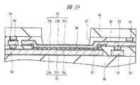
前記実施の形態1では、中間配線39が上層の配線に接続される例について説明したが、本実施の形態2では、中間配線39が上層の配線だけでなく下層の配線にも接続される製造方法について、図面を参照しながら説明する。
(Embodiment 2)
In the first embodiment, the example in which the
まず、図13に示すように、絶縁膜30上に窒化チタン膜31a、アルミニウム膜31bおよび窒化チタン膜31cを順次、積層して形成する。窒化チタン膜31a、アルミニウム膜31bおよび窒化チタン膜31cは、例えば、スパッタリング法を使用して形成することができる。続いて、フォトリソグラフィ技術およびエッチング技術を使用して、窒化チタン膜31a、アルミニウム膜31bおよび窒化チタン膜31cをパターニングする。これにより、窒化チタン膜31a、アルミニウム膜31bおよび窒化チタン膜31cよりなる下部電極(第1電極)32および下層配線53が形成される。そして、下部電極32および下層配線53を含む絶縁膜30上に絶縁膜(第1絶縁膜)33を形成する。この絶縁膜33も、例えばCVD法を使用した酸化シリコン膜より形成することができる。
First, as shown in FIG. 13, a
続いて、フォトリソグラフィ技術およびエッチング技術を使用して、絶縁膜33に接続孔を形成する。形成される接続孔の一つは下部電極32に達し、他の接続孔の一つは下層配線53に達している。そして、接続孔内を含む絶縁膜33上に、窒化チタン膜およびタングステン膜からなる積層膜を形成した後、CMP技術を使用して接続孔内にだけ積層膜を残すことにより、プラグ54およびプラグ55を形成する。
Subsequently, a connection hole is formed in the insulating
次に、図14に示すように、絶縁膜33上にレジスト膜34を塗布した後、レジスト膜34に対して露光・現像処理を施すことにより、レジスト膜34をパターニングする。パターニングは、開口部35を形成する領域にレジスト膜34が残らないようにする。次に、パターニングしたレジスト膜34をマスクにして絶縁膜33をエッチングする。これにより、絶縁膜33に開口部(第1開口部)35が形成される。この開口部35の底部には、下部電極32が露出している。
Next, as shown in FIG. 14, after a resist
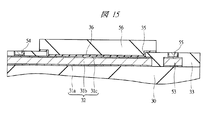
次に、レジスト膜34を除去した後、図15に示すように、開口部35内を含む絶縁膜33上に容量絶縁膜(第1容量絶縁膜)36を形成する。そして、容量絶縁膜36上にレジスト膜56を塗布した後、露光・現像処理を施すことにより、パターニングする。パターニングは、容量絶縁膜36を残す領域にレジスト膜56が残るようにする。
Next, after removing the resist
続いて、図16に示すように、レジスト膜56を除去した後、容量絶縁膜36を含む絶縁膜33上に窒化チタン膜37a、アルミニウム膜37bおよび窒化チタン膜37cを順次、スパッタリング法で形成する(第1導体膜)。その後、窒化チタン膜37c上にレジスト膜57を塗布し、塗布したレジスト膜57に対して露光・現像処理を施す。これにより、レジスト膜57をパターニングする。パターニングは、中間電極形成領域および配線形成領域にレジスト膜57が残るようにする。続いて、パターニングしたレジスト膜57をマスクにしたエッチングにより、中間電極(第2電極)39および配線58を形成する。
Subsequently, as shown in FIG. 16, after removing the resist
ここで、前記実施の形態1では、容量絶縁膜36、窒化チタン膜37a、アルミニウム膜37bおよび窒化チタン膜37cを順次積層した後、パターニングして中間電極39を形成していた。しかし、この方法では、中間電極39とプラグ55との間に容量絶縁膜36が形成されてしまうため、中間電極39と下層配線53との導通がとれなくなってしまう。そこで、本実施の形態2では、まず、容量絶縁膜36を形成した後にパターニングしてプラグ55上に容量絶縁膜が残らないようにしている。そしてその後、中間電極39を形成することにより、中間電極39と下層配線53とをプラグ55を介して電気接続するようにしている。これにより、中間電極39を下層配線53に電気接続することができる。
Here, in the first embodiment, the capacitive insulating
次に、レジスト膜57を除去した後、図17に示すように、中間電極39上を含む絶縁膜33上に絶縁膜(第2絶縁膜)40を形成する。絶縁膜40は、例えば、CVD法を用いた酸化シリコン膜より形成することができる。続いて、絶縁膜40上にレジスト膜41を塗布した後、露光・現像処理を施すことにより、レジスト膜41をパターニングする。パターニングは、接続孔形成領域にレジスト膜41が残らないようにする。そして、パターニングしたレジスト膜41をマスクにしたエッチングにより、接続孔43および接続孔59を形成する。接続孔43は中間電極39に達しており、接続孔59は配線58に達している。
Next, after removing the resist
次に、レジスト膜41を除去した後、図18に示すように、接続孔43および接続孔59に導電材料を埋め込んでプラグ60およびプラグ61を形成する。プラグ60およびプラグ61は、例えば窒化チタン膜およびタングステン膜の積層膜を、接続孔43、59内を含む絶縁膜40上に形成した後、CMP法を使用して絶縁膜40上に形成された積層膜を研磨することにより形成される。
Next, after removing the resist
続いて、図19に示すように、絶縁膜40上にレジスト膜46を塗布した後、露光・現像処理を施すことにより、レジスト膜46をパターニングする。パターニングは、開口部形成領域にレジスト膜46が残らないようにする。そして、パターニングしたレジスト膜46をマスクにしてエッチングすることにより、開口部(第2開口部)47を形成する。
Subsequently, as shown in FIG. 19, after a resist
次に、図20に示すように、開口部47内を含む絶縁膜40上に容量絶縁膜(第2容量絶縁膜)48および窒化チタン膜49を積層して形成する。そして、窒化チタン膜49上にレジスト膜50を塗布した後、露光・現像処理を施すことにより、レジスト膜50をパターニングする。続いて、パターニングしたレジスト膜50をマスクにして、容量絶縁膜48および窒化チタン膜49をエッチングする。
Next, as shown in FIG. 20, a capacitor insulating film (second capacitor insulating film) 48 and a
次に、図21に示すように、パターニングした窒化チタン膜49を含む絶縁膜40上に、窒化チタン膜51a、アルミニウム膜51bおよび窒化チタン膜51cを順次、スパッタリング法で形成する(第2導体膜)。その後、フォトリソグラフィ技術およびエッチング技術を使用して、これらの膜をパターニングすることにより、窒化チタン膜51a、アルミニウム膜51bおよび窒化チタン膜51cよりなる上部電極(第3電極)52を形成することができる。このようにして、中間電極39を上下層の配線に接続することができる。本実施の形態2によれば、一般配線に接続する中間電極39を上層配線だけでなく、下層配線にも接続できるので、配線形成の自由度を増大することができる。なお、本実施の形態2によれば、前記実施の形態1と同様の効果を得ることができる。
Next, as shown in FIG. 21, a
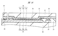
(実施の形態3)
本実施の形態3では、積層構造で可変容量を形成する例について説明する。図22は、本実施の形態3における容量素子を示した平面図である。図22において、下部電極10が形成されており、この下部電極10上には絶縁膜(図示せず)を介して中間電極11が形成されている。この下部電極10と中間電極11が平面上で重なり合う領域に容量素子Caが形成されている。さらに、中間電極11上には、絶縁膜(図示せず)を介して上部電極12a〜12cおよび配線13が形成されている。中間電極11と上部電極12aが平面的に重なり合う領域には、容量素子Cbが形成されており、中間電極11と上部電極12bが平面的に重なり合う領域には、容量素子Ccが形成されている。さらに、中間電極11と上部電極12cが平面的に重なり合う領域には、容量素子Cdが形成されている。このように本実施の形態3では、容量素子Ca上に容量素子Cb、Cc、Cdが形成された構造をしている。上部電極12a〜12cは、例えばプラグ14を介して下部電極10に接続されており、中間電極11は、例えばプラグ15を介して配線13に接続されている。したがって、容量素子Ca、Cb、Cc、Cdは、互いに並列接続されている。このときの回路図を図24に示す。図24に示すように、容量素子Ca、Cb、Cc、Cdは、並列接続されており、それぞれの容量素子にはスイッチが設けられている。これにより、可変容量素子を形成することができる。例えば、容量素子Caに接続されているスイッチだけをオンにすると、可変容量素子の容量は容量素子Caの容量になる。また、容量素子Caのスイッチと容量素子Cbのスイッチをオンにすると、可変容量素子の容量は、容量素子Caの容量と容量素子Cbの容量との和になる。このようにスイッチを適宜選択することにより、所望の容量を得ることができる。本実施の形態3によれば、積層化された複数の容量素子とスイッチを組み合わせることで、容量素子の占有面積を低減させながら柔軟度の高い可変容量素子を形成することができる。
(Embodiment 3)
In the third embodiment, an example in which a variable capacitor is formed with a stacked structure will be described. FIG. 22 is a plan view showing the capacitive element according to the third embodiment. In FIG. 22, a
図23は、図22のA−A線で切断した断面図を示したものである。図23の構成は、前記実施の形態1とほぼ同様の構成をしており、異なる点は、上部電極12bおよび上部電極12cが設けられている点である。すなわち、本実施の形態3では、中間電極11と上部電極12bによって容量素子Ccが形成され、中間電極11と上部電極12cによって容量素子Cdが形成されている。中間電極11は、前記実施の形態1と同様に段差が設けられている。つまり、容量素子形成領域(開口部内)では、中間電極11と下部電極10の距離は小さくなっている一方、容量素子形成領域以外の領域(開口部の外側)では、中間電極11と下部電極10との距離が大きくなっている。同様に、中間電極11と上部電極12b、12cとの間でも寄生容量の低減が図られている。これにより、中間電極11と下部電極10との間の寄生容量を低減することができるので、中間電極11を一般配線に使用したときの信号遅延および消費電力の増加を抑制できる。
FIG. 23 shows a cross-sectional view taken along line AA in FIG. The configuration of FIG. 23 is substantially the same as that of the first embodiment, and the difference is that an
なお、本実施の形態3における可変容量素子の製造方法は、前記実施の形態1と基本的に同様である。特徴点は、図23に示すように、中間電極11上に形成された絶縁膜22に二つの開口部を形成し、一方の開口部に容量絶縁膜21および上部電極12bを形成することにより、容量素子Ccを形成している。また、他方の開口部に容量絶縁膜21および上部電極12cを形成することにより、容量素子Cdを形成している。これらの構造は、フォトリソグラフィ技術によるパターニングを変えることで実現することができる。
The manufacturing method of the variable capacitance element in the third embodiment is basically the same as that in the first embodiment. As shown in FIG. 23, the feature point is that by forming two openings in the insulating
(実施の形態4)
本実施の形態4は、開口部の側壁にサイドウォールを形成した容量素子について説明する。図25は、図3に示す容量素子の開口部19a付近を拡大した断面図である。図25において、アルミニウム膜17b上には窒化チタン膜17cが形成されており、この窒化チタン膜17c上に絶縁膜19が形成されている。そして、絶縁膜19には、開口部19aが形成されており、この開口部19aの底面および側面には容量絶縁膜18が形成されている。なお、図示はされていないが、容量絶縁膜18上には上部電極12が形成されている。
(Embodiment 4)
In the fourth embodiment, a capacitor element in which a sidewall is formed on the side wall of the opening will be described. 25 is an enlarged cross-sectional view of the vicinity of the
ここで、絶縁膜19に開口部19aを形成する際、エッチング技術が使用されるが、このとき、オーバーエッチングにより開口部19aの底部に露出する窒化チタン膜17cの一部もエッチングされる。そして、開口部19aの底面および側面を含む絶縁膜19上に容量絶縁膜18が形成される。容量絶縁膜18は、例えばプラズマCVD法によって形成されるが、プラズマCVD法では、開口部19aの底面に形成される容量絶縁膜18の膜厚と開口部19aの側面に形成される容量絶縁膜18の膜厚が異なる。すなわち、開口部19aの底面に比べて開口部19aの側面では、形成される容量絶縁膜18の膜厚が薄くなる。このように、窒化チタン膜17cのエッチングおよび開口部19aの側面で容量絶縁膜18の膜厚が薄くなる現象から、開口部19aの角部で、容量素子の耐圧が低下する問題が生じる。
Here, when forming the
そこで、本実施の形態4では、図26に示すように、開口部19aの側面に絶縁体膜からなるサイドウォール65を設けている。そして、このサイドウォール65上に容量絶縁膜18を設けることにより、開口部19aの角部における絶縁膜の厚さを確保できるので、容量素子の耐圧を向上させることができる。すなわち、開口部19aの側面には、容量絶縁膜18の他にサイドウォール65を形成しているので、窒化チタン膜17cの一部がエッチングによって削られても、開口部19aの角部における中間電極と上部電極との距離を大きくすることができる。このため、開口部19aの角部におけるリーク電流を抑制することができ、容量素子の耐圧向上を図ることができる。
Therefore, in the fourth embodiment, as shown in FIG. 26, a
次に、本実施の形態4における容量素子の製造方法について説明する。図27に示すように、絶縁膜30上に窒化チタン膜31a、アルミニウム膜31bおよび窒化チタン膜31cを順次、積層して形成する。窒化チタン膜31a、アルミニウム膜31bおよび窒化チタン膜31cは、例えば、スパッタリング法を使用して形成することができる。続いて、フォトリソグラフィ技術およびエッチング技術を使用して、窒化チタン膜31a、アルミニウム膜31bおよび窒化チタン膜31cをパターニングする。これにより、窒化チタン膜31a、アルミニウム膜31bおよび窒化チタン膜31cよりなる下部電極32が形成される。そして、下部電極32を含む絶縁膜30上に絶縁膜33を形成する。この絶縁膜33も、例えばCVD法を使用した酸化シリコン膜より形成することができる。
Next, a method for manufacturing the capacitive element in the fourth embodiment will be described. As shown in FIG. 27, a
続いて、図28に示すように、絶縁膜33上にレジスト膜34を塗布した後、レジスト膜34に対して露光・現像処理を施すことにより、レジスト膜34をパターニングする。パターニングは、開口部35を形成する領域にレジスト膜34が残らないようにする。次に、パターニングしたレジスト膜34をマスクにして絶縁膜33をエッチングする。これにより、絶縁膜33に開口部35が形成される。この開口部35の底部には、下部電極32が露出している。
Subsequently, as shown in FIG. 28, after a resist
次に、図29に示すように、開口部35内を含む絶縁膜33上に例えば酸化シリコン膜よりなる絶縁膜(第3絶縁膜)66を形成する。絶縁膜66は例えばCVD法を使用して形成することができる。その後、図30に示すように、絶縁膜66を異方性エッチングすることにより、開口部35の側壁にだけ絶縁膜66を残してサイドウォール67を形成する。なお、サイドウォール67は、下地である窒化チタン膜17cと選択比がとれればよいので、酸化シリコン膜に限らず他の絶縁膜であってもよい。
Next, as shown in FIG. 29, an insulating film (third insulating film) 66 made of, for example, a silicon oxide film is formed on the insulating
続いて、レジスト膜34を除去した後、図31に示すように、開口部35内を含む絶縁膜33上に容量絶縁膜36を形成する。容量絶縁膜36は、例えば、CVD法を使用して形成することができる。そして、容量絶縁膜36上に窒化チタン膜37a、アルミニウム膜37bおよび窒化チタン膜37cを順次、スパッタリング法で形成する。その後、窒化チタン膜37c上にレジスト膜38を塗布し、塗布したレジスト膜38に対して露光・現像処理を施す。これにより、レジスト膜38をパターニングする。パターニングは、中間電極形成領域にレジスト膜38が残るようにする。続いて、パターニングしたレジスト膜38をマスクにしたエッチングにより、中間電極39を形成する。
Subsequently, after removing the resist
その後、レジスト膜38を除去した後、中間電極39上を含む絶縁膜33上に絶縁膜40を形成し、この絶縁膜40に開口部47を形成する。そして、開口部47内を含む絶縁膜40上に絶縁膜を形成した後、この絶縁膜を異方性エッチングすることにより、サイドウォール68を形成する。その後は、前記実施の形態1と同様の工程を経ることにより、図32に示す容量素子を形成することができる。
Thereafter, after removing the resist
本実施の形態4によれば、電極間の寄生容量を低減できるとともに、サイドウォール67、68を設けることにより、容量素子の耐圧向上を図ることができる。なお、本実施の形態4では、サイドウォール67、68を設けることにより、容量素子の耐圧を向上させているが、例えば図33に示すように、エッチング技術を改良することによって、窒化チタン膜17cの削れ量を抑制し、開口部19aの角部における耐圧を向上させてもよい。すなわち、窒化チタン膜17cの削れ量が抑制されれば、開口部19aの角部において、上部電極と中間電極との距離が必要以上に近づくことがなくなり、リーク電流を抑制できるので、容量素子の耐圧を向上できる。
According to the fourth embodiment, the parasitic capacitance between the electrodes can be reduced, and by providing the
(実施の形態5)
本実施の形態5では、3つの容量素子を積層した構造の容量素子について説明する。図34は、本実施の形態5における容量素子を示した断面図である。図34において、2つの容量素子(第1容量素子および第2容量素子)が積層されている下部電極32から上部電極52までの構造は、前記実施の形態1と同様である。本実施の形態5では、上部電極52上に絶縁膜70が形成されており、この絶縁膜70に開口部71が形成されている。開口部71内を含む絶縁膜70上には、容量絶縁膜72、窒化チタン膜73および最上部電極75が形成されている。最上部電極75は、例えば窒化チタン膜74a、アルミニウム膜74bおよび窒化チタン膜74cの積層膜から構成されている。
(Embodiment 5)
In the fifth embodiment, a capacitor having a structure in which three capacitors are stacked will be described. FIG. 34 is a cross-sectional view showing the capacitive element in the fifth embodiment. In FIG. 34, the structure from the
このように本実施の形態5では、下部電極32、容量絶縁膜36および中間電極39よりなる第1容量素子上に、中間電極39、容量絶縁膜48および上部電極52よりなる第2容量素子が形成されている。そして、さらに、第2容量素子上に、上部電極52、容量絶縁膜72および最上部電極75よりなる第3容量素子が形成されている。これら第1容量素子、第2容量素子および第3容量素子は、並列接続されており、3つの容量素子が積層した構造となっている。したがって、本実施の形態5によれば、容量素子の占有面積を低減しながら、大きな容量を確保することができる。すなわち、本実施の形態5によれば、3つの容量素子を積層した構造をしているので、2つの容量素子を積層した構造に比べて、さらに大きな容量を確保することができる。
As described above, in the fifth embodiment, the second capacitive element including the
(実施の形態6)
本実施の形態6では、2つの容量素子を積層した構造の容量素子と、積層構造を有さない容量素子とを設ける例について説明する。図35は、本実施の形態6における容量素子を示した断面図である。図35に示すように、本実施の形態6における容量素子は、2つの容量素子を積層した構造の容量素子76と単層構造の容量素子(第4容量素子)77が設けられている。容量素子76は、前記実施の形態1で説明した容量素子と同様である。
この容量素子76と容量素子77は、互いに並列接続されており、容量素子77をオン/オフするスイッチが設けられている。このように構成することで、容量の微調整が可能となる。すなわち、容量素子76は積層構造をしているので大きな容量をしている。一方、容量素子77は単層構造をしているので小さな容量をしている。ここで、容量素子77に接続されたスイッチをオンすることで、容量素子76だけの容量から容量素子77の容量だけ増加させることができる。回路の特性などの関係から容量素子76の容量からわずかに容量を増加させたい場合には、低容量の容量素子77に接続されたスイッチをオンさせることで対応できる。このように本実施の形態6によれば、積層構造をした容量素子76と単層構造をした容量素子77を組み合わせることにより、容量の微調整が可能となる。
(Embodiment 6)
In the sixth embodiment, an example in which a capacitor element having a structure in which two capacitor elements are stacked and a capacitor element having no stacked structure will be described. FIG. 35 is a cross-sectional view showing the capacitive element in the sixth embodiment. As shown in FIG. 35, the capacitive element according to the sixth embodiment is provided with a
The
(実施の形態7)
本実施の形態7では、前記実施の形態1〜6で説明した容量素子を使用する電子装置について説明する。電子装置の一例として携帯電話機を説明する。図36は、携帯電話機における送受信部の構成を示したブロック図である。図36に示すように、送受信部80は、アンテナ81、アンテナスイッチ82、RF(Radio Frequency)フィルタ83、RF−IC(送受信装置)84、ベースバンド部85およびPAモジュール86を有している。さらに、RF−IC84は、LNA(Low Noise Amplifier)87、PGA88、TXVCO(電圧制御発振器)89、RFVCO90、IFVCO91、DC/VCXO92などから構成されている。
(Embodiment 7)
In Embodiment 7, an electronic device using the capacitor described in
まず、携帯電話機において電波を受信する動作の一例について簡単に説明する。アンテナ81で受信したRF信号は、アンテナスイッチ82によって受信側に伝達される。そして、受信したRF信号は、RFフィルタ83を介してRF−IC84に入力される。RF−IC84に入力されたRF信号は、LNA87で増幅される。その後、増幅された信号をダイレクトコンバージョンミキサにて直交復調することで、直接ベースバンド信号が得られる。このベースバンド信号は、それぞれPGA88で利得調節されて、ベースバンド部85に送られて処理される。このようにして電波を受信することができる。
First, an example of an operation for receiving radio waves in a mobile phone will be briefly described. The RF signal received by the
次に、携帯電話機において電波を送信する動作の一例について簡単に説明する。ベースバンド部85よりベースバンド信号がRF−IC84に入力されると、RF−IC84では、IF信号をベースバンド信号で直交変調する。そして、TXVCO89を含むPLL回路でIF信号を周波数変換してRF信号が得られる。RF−IC84のシンセサイザは、内蔵されているRFVCO90、IFVCO91や分周器を介して各ブロックにローカル信号を供給している。また、基準クロックは、DC/VCXO92にて生成している。
RF−IC84で生成されたRF信号は、PAモジュール86で増幅される。そして、アンテナスイッチ82を介してアンテナ81からRF信号が送信される。このようにして電波を送信することができる。
Next, an example of an operation for transmitting radio waves in the mobile phone will be briefly described. When a baseband signal is input to the RF-
The RF signal generated by the RF-
RF−IC84には、図36に示すように様々な回路が形成されているが、これらの回路は一つの半導体チップに搭載されている。すなわち、一つの半導体チップ上にRF−ICが形成されている。図37は、LNA87の回路の一例を示したものである。図37に示すように、LNA87には、複数の容量素子が使用されていることがわかる。LNA87は、低雑音の増幅器であり、このLNA87の入力部に設けられている容量素子は、インピーダンスマッチングを行なうために使用されている。
Various circuits are formed in the RF-
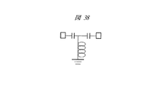
図38は、PGA88に含まれるバンドパスフィルタの一例を示したものである。図38に示すバンドパスフィルタは、所定の周波数範囲の信号だけを通過させる機能を有しており、複数の容量素子が使用されていることがわかる。
FIG. 38 shows an example of a bandpass filter included in the
図39および図40は、電圧制御発振器の一例を示した図である。図39および図40に示す電圧制御発振器は、負性抵抗を加えるアンプ回路とLC共振回路からなる差動タイプの発振器であり、複数の容量素子が使用されていることがわかる。このようにRF―IC84に形成されている回路には、複数の容量素子が使用されているが、これらの容量素子は、高周波特性およびノイズ特性により、寄生抵抗や寄生容量の少ない低損失なものが要求される。そこで、RF−IC84に前記実施の形態1〜6で説明した容量素子を用いることにより、容量素子の寄生容量を低減できるので、RF−IC84に対して低損失で高性能の容量素子を提供できる。
39 and 40 are diagrams illustrating an example of a voltage controlled oscillator. The voltage controlled oscillator shown in FIGS. 39 and 40 is a differential type oscillator composed of an amplifier circuit for adding a negative resistance and an LC resonance circuit, and it can be seen that a plurality of capacitive elements are used. In this way, the circuit formed in the RF-
RF−IC84の各回路は、例えば図37〜図40に示すように、多数の容量素子を使用している。これらの容量素子の容量はRF−IC全体で10nF前後の容量となり、これらの容量をゲート容量(拡散容量)で構成した場合、約2.5mm2の面積が必要となる。ここで、ゲート容量の単位容量を例えば4fF/μm2としている。
Each circuit of the RF-
また、RF−IC84は一般に3層〜6層の多層配線で構成されているが、現状の配線使用面積は、1層あたり20%〜40%で未使用の面積が多数を占めている。このため、RF−IC84に使用される容量素子として、本実施の形態1〜6に示す容量素子を使用することにより、多層配線中に容量素子を効率良く配置すれば、ゲート容量形成領域の面積を低減することができる。例えば、3.5mm×3.5mmの半導体チップの場合、2.5mm2のゲート容量の部分を多層配線間に形成すると、必要な半導体チップのサイズは、3.5mm×3.5mm−2.5mm2=9.75mm2となり、約20%の面積低減が可能となる。その結果、シリコンウェハ1枚から取得できる半導体チップの数も約20%増加でき、半導体チップ1個あたりの製造コストも低減することができる。
The RF-
また、RF−IC84では、電源電圧を低減しにくく各素子にある程度の耐圧が必要とされる。ここで、前記実施の形態4で説明したようにサイドウォールを設けることにより、容量素子の耐圧を向上することができる。したがって、RF−IC84に使用する容量素子として、前記実施の形態4で説明した容量素子を用いることにより、耐圧を向上させることができ、RF−IC84の信頼性向上を図ることができる。
Further, in the RF-
なお、本実施の形態7では、RF−IC84に前記実施の形態1〜6における容量素子を適用する例について説明したが、これに限らず、例えばPAモジュール86に適用してもよい。
In the seventh embodiment, the example in which the capacitive element in the first to sixth embodiments is applied to the RF-
以上、本発明者によってなされた発明を実施の形態に基づき具体的に説明したが、本発明は前記実施の形態に限定されるものではなく、その要旨を逸脱しない範囲で種々変更可能であることはいうまでもない。 As mentioned above, the invention made by the present inventor has been specifically described based on the embodiment. However, the present invention is not limited to the embodiment, and various modifications can be made without departing from the scope of the invention. Needless to say.
本発明は、半導体装置を製造する製造業に幅広く利用することができる。 The present invention can be widely used in the manufacturing industry for manufacturing semiconductor devices.
1 半導体基板
2 nチャネル型MISFET
3 pチャネル型MISFET
4 容量素子
10 下部電極
11 中間電極
12 上部電極
13 配線
14 プラグ
15 プラグ
16 絶縁膜
17a 窒化チタン膜
17b アルミニウム膜
17c 窒化チタン膜
18 容量絶縁膜
19 絶縁膜
19a 開口部
20a 窒化チタン膜
20b アルミニウム膜
20c 窒化チタン膜
21 容量絶縁膜
22 絶縁膜
22a 開口部
23 窒化チタン膜
24a 窒化チタン膜
24b アルミニウム膜
24c 窒化チタン膜
30 絶縁膜
31a 窒化チタン膜
31b アルミニウム膜
31c 窒化チタン膜
32 下部電極
33 絶縁膜
34 レジスト膜
35 開口部
36 容量絶縁膜
37a 窒化チタン膜
37b アルミニウム膜
37c 窒化チタン膜
38 レジスト膜
39 中間電極
40 絶縁膜
41 レジスト膜
42 接続孔
43 接続孔
44 プラグ
45 プラグ
46 レジスト膜
47 開口部
48 容量絶縁膜
49 窒化チタン膜
50 レジスト膜
51a 窒化チタン膜
51b アルミニウム膜
51c 窒化チタン膜
52 上部電極
53 下層配線
54 プラグ
55 プラグ
56 レジスト膜
57 レジスト膜
58 配線
59 接続孔
60 プラグ
61 プラグ
66 絶縁膜
67 サイドウォール
68 サイドウォール
70 絶縁膜
71 開口部
72 容量絶縁膜
73 窒化チタン膜
74a 窒化チタン膜
74b アルミニウム膜
74c 窒化チタン膜
75 最上部電極
76 容量素子
77 容量素子
80 送受信部
81 アンテナ
82 アンテナスイッチ
83 RFフィルタ
84 RF−IC
85 ベースバンド部
86 PAモジュール
87 LNA
88 PGA
89 TXVCO
90 RFVCO
91 IFVCO
92 DC/VCXO
100 下部電極
101 容量絶縁膜
102 中間電極
103 容量絶縁膜
104 上部電極
C1 容量素子
C2 容量素子
Ca〜Cd 容量素子
1 Semiconductor substrate 2 n-channel MISFET
3 p-channel MISFET
4
85
88 PGA
89 TXVCO
90 RFVCO
91 IFVCO
92 DC / VCXO
100
Claims (18)
前記第1電極上に形成された第1絶縁膜と、
前記第1絶縁膜に形成され、且つ、前記第1電極が露出するように形成された第1開口部と、
前記第1開口部の側壁に形成され、且つ、第3絶縁膜からなる第1サイドウォールと、
前記第1絶縁膜上に形成され、且つ、前記第1開口部内にて前記第1サイドウォールを覆うように前記第1電極上に形成された第1容量絶縁膜と、
前記第1容量絶縁膜上に形成された第2電極と、
前記第2電極上に形成された第2絶縁膜と、
前記第2絶縁膜に形成され、且つ、前記第2電極が露出するように形成された第2開口部と、
前記第2開口部の側壁に形成され、且つ、第4絶縁膜からなる第2サイドウォールと、
前記第2絶縁膜上に形成され、且つ、前記第2開口部内にて前記第2サイドウォールを覆うように前記第2電極上に形成された第2容量絶縁膜と、
前記第2容量絶縁膜上に形成された第3電極と、を備えることを特徴とする半導体装置。 A first electrode;
A first insulating film formed on the first electrode;
A first opening formed in the first insulating film and formed to expose the first electrode;
A first sidewall formed on a sidewall of the first opening and made of a third insulating film;
A first capacitance insulating film formed on the first insulating film and on the first electrode so as to cover the first sidewall in the first opening ;
A second electrode formed on the first capacitive insulating film,
A second insulating film formed on the second electrode;
A second opening formed in the second insulating film and formed to expose the second electrode;
A second sidewall formed on a sidewall of the second opening and made of a fourth insulating film;
A second capacitor insulating film formed on the second insulating film and on the second electrode so as to cover the second sidewall in the second opening ;
The semiconductor device according to claim a third electrode formed on the second capacitive insulating film, that Ru comprising a.
前記第1容量絶縁膜と前記第1電極の接触面積は、前記第2容量絶縁膜と前記第2電極の接触面積よりも大きいことを特徴とする半導体装置。 In claim 1,
The contact area between the first capacitor insulating film and the first electrode is larger than the contact area between the second capacitor insulating film and the second electrode.
前記第2電極は、信号配線あるいは電源配線に使用されることを特徴とする半導体装置。 In claim 1 or 2 ,
The semiconductor device, wherein the second electrode is used for signal wiring or power wiring.
前記第1電極と前記第3電極とは、電気的に接続されていることを特徴とする半導体装置。 In any one of claims 1 to 3,
The semiconductor device, wherein the first electrode and the third electrode are electrically connected.
前記第1電極、前記第1容量絶縁膜および前記第2電極からなる第1容量素子と、前記第2電極、前記第2容量絶縁膜および前記第3電極からなる第2容量素子は、並列接続されていることを特徴とする半導体装置。 In claim 4 ,
A first capacitive element comprising the first electrode, the first capacitive insulating film and the second electrode, and a second capacitive element comprising the second electrode, the second capacitive insulating film and the third electrode are connected in parallel. A semiconductor device which is characterized by being made.
前記第1電極、前記第2電極および前記第3電極は、アルミニウム膜あるいはタングステン膜から形成されていることを特徴とする半導体装置。 In any one of Claims 1-5 ,
The semiconductor device, wherein the first electrode, the second electrode, and the third electrode are formed of an aluminum film or a tungsten film.
前記第1容量絶縁膜および前記第2容量絶縁膜は、酸化シリコン膜、窒化シリコン膜、アルミナ膜、タンタルあるいはハフニウムの酸化物を含む膜のいずれかより形成されていることを特徴とする半導体装置。 In any one of Claims 1-6 ,
The first capacitor insulating film and the second capacitor insulating film are formed of any one of a silicon oxide film, a silicon nitride film, an alumina film, a film containing an oxide of tantalum or hafnium. .
前記第1開口部内において、前記第1サイドウォールを介して前記第1開口部の側壁に形成されている前記第1容量絶縁膜の膜厚は、前記第1電極上に形成されている前記第1容量絶縁膜の膜厚よりも薄いことを特徴とする半導体装置。In the first opening, the thickness of the first capacitor insulating film formed on the side wall of the first opening via the first sidewall is the thickness of the first capacitor insulating film formed on the first electrode. A semiconductor device characterized in that it is thinner than the film thickness of one capacitor insulating film.
前記第2開口部内において、前記第2サイドウォールを介して前記第2開口部の側壁に形成されている前記第2容量絶縁膜の膜厚は、前記第2電極上に形成されている前記第2容量絶縁膜の膜厚よりも薄いことを特徴とする半導体装置。In the second opening, the thickness of the second capacitor insulating film formed on the side wall of the second opening through the second sidewall is the second thickness formed on the second electrode. A semiconductor device characterized by being thinner than the film thickness of a two-capacity insulating film.
前記第1開口部内において、前記第1容量絶縁膜は、前記第1電極および前記第1サイドウォールと直接接していることを特徴とする半導体装置。In the first opening, the first capacitor insulating film is in direct contact with the first electrode and the first sidewall.
前記第2開口部内において、前記第2容量絶縁膜は、前記第2電極および前記第2サイドウォールと直接接していることを特徴とする半導体装置。In the second opening, the second capacitor insulating film is in direct contact with the second electrode and the second sidewall.
(b)前記第1電極上に第1絶縁膜を形成する工程と、
(c)前記第1絶縁膜に前記第1電極に達する第1開口部を形成する工程と、
(d)前記第1開口部の側壁に、第3絶縁膜からなる第1サイドウォールを形成する工程と、
(e)前記第1絶縁膜上に第1容量絶縁膜を形成する工程であって、前記第1開口部内にて前記第1サイドウォールを覆うように前記第1電極上に前記第1容量絶縁膜を形成する工程と、
(f)前記第1開口部内を含む前記第1容量絶縁膜上に第1導体膜を形成する工程と、
(g)前記第1導体膜をパターニングして第2電極を形成する工程と、
(h)前記第2電極上に第2絶縁膜を形成する工程と、
(i)前記第2絶縁膜に前記第2電極に達する第2開口部を形成する工程と、
(j)前記第2開口部の側壁に、第4絶縁膜からなる第2サイドウォールを形成する工程と、
(k)前記第2絶縁膜上に第2容量絶縁膜を形成する工程であって、前記第2開口部内にて前記第2サイドウォールを覆うように前記第2電極上に前記第2容量絶縁膜を形成する工程と、
(l)前記第2開口部内を含む前記第2容量絶縁膜上に第2導体膜を形成する工程と、
(m)前記第2導体膜をパターニングして第3電極を形成する工程と、を備えることを特徴とする半導体装置の製造方法。 (A) forming a first electrode on a semiconductor substrate;
(B) forming a first insulating film on the first electrode;
(C) forming a first opening reaching the first electrode in the first insulating film;
(D) forming a first sidewall made of a third insulating film on the sidewall of the first opening;
( E ) forming a first capacitive insulating film on the first insulating film, wherein the first capacitive insulating film is formed on the first electrode so as to cover the first sidewall in the first opening. Forming a film ;
( F ) forming a first conductor film on the first capacitive insulating film including the inside of the first opening;
( G ) patterning the first conductor film to form a second electrode;
( H ) forming a second insulating film on the second electrode ;
( I ) forming a second opening reaching the second electrode in the second insulating film;
(J) forming a second sidewall made of a fourth insulating film on the sidewall of the second opening;
( K ) forming a second capacitive insulating film on the second insulating film, wherein the second capacitive insulating film is formed on the second electrode so as to cover the second sidewall in the second opening. Forming a film ;
( L ) forming a second conductor film on the second capacitive insulating film including the inside of the second opening;
(M) a method of manufacturing a semiconductor device, characterized in that it comprises a step of forming a third electrode by patterning the second conductive film.
前記第1開口部内において、前記第1サイドウォールを介して前記第1開口部の側壁に形成されている前記第1容量絶縁膜の膜厚は、前記第1電極上に形成されている前記第1容量絶縁膜の膜厚よりも薄いことを特徴とする半導体装置の製造方法。In the first opening, the thickness of the first capacitor insulating film formed on the side wall of the first opening via the first sidewall is the thickness of the first capacitor insulating film formed on the first electrode. A method for manufacturing a semiconductor device, characterized in that the thickness is smaller than a film thickness of a one-capacity insulating film.
前記第2開口部内において、前記第2サイドウォールを介して前記第2開口部の側壁に形成されている前記第2容量絶縁膜の膜厚は、前記第2電極上に形成されている前記第2容量絶縁膜の膜厚よりも薄いことを特徴とする半導体装置の製造方法。In the second opening, the thickness of the second capacitor insulating film formed on the side wall of the second opening through the second sidewall is the second thickness formed on the second electrode. A method of manufacturing a semiconductor device, wherein the thickness is smaller than a film thickness of a two-capacity insulating film.
前記第1開口部内において、前記第1容量絶縁膜は、前記第1電極および前記第1サイドウォールと直接接していることを特徴とする半導体装置の製造方法。In the first opening, the first capacitor insulating film is in direct contact with the first electrode and the first sidewall.
前記第2開口部内において、前記第2容量絶縁膜は、前記第2電極および前記第2サイドウォールと直接接していることを特徴とする半導体装置の製造方法。In the second opening, the second capacitor insulating film is in direct contact with the second electrode and the second sidewall.
前記(d)工程は、The step (d)
(d1)前記第1絶縁膜上、及び、前記第1開口部にて前記第1電極上に前記第3絶縁膜を形成する工程と、(D1) forming the third insulating film on the first insulating film and on the first electrode in the first opening;
(d2)前記第3絶縁膜を異方性エッチングすることにより、前記第1開口部の側壁に前記第3絶縁膜を残すことで、前記第1サイドウォールを形成する工程と、を有することを特徴とする半導体装置の製造方法。(D2) forming the first side wall by anisotropically etching the third insulating film to leave the third insulating film on the side wall of the first opening. A method of manufacturing a semiconductor device.
前記(j)工程は、The step (j)
(j1)前記第2絶縁膜上、及び、前記第2開口部にて前記第2電極上に前記第4絶縁膜を形成する工程と、(J1) forming the fourth insulating film on the second insulating film and on the second electrode in the second opening;
(j2)前記第4絶縁膜を異方性エッチングすることにより、前記第2開口部の側壁に前記第4絶縁膜を残すことで、前記第2サイドウォールを形成する工程と、を有することを特徴とする半導体装置の製造方法。(J2) forming the second side wall by anisotropically etching the fourth insulating film to leave the fourth insulating film on the side wall of the second opening. A method of manufacturing a semiconductor device.
Priority Applications (5)
| Application Number | Priority Date | Filing Date | Title |
|---|---|---|---|
| JP2005186967A JP4928748B2 (en) | 2005-06-27 | 2005-06-27 | Semiconductor device and manufacturing method thereof |
| US11/473,229 US20060289917A1 (en) | 2005-06-27 | 2006-06-23 | Semiconductor device, RF-IC and manufacturing method of the same |
| CNA2006100935372A CN1893067A (en) | 2005-06-27 | 2006-06-26 | Semiconductor device, RF-IC and manufacturing method of the same |
| US12/565,963 US20100013568A1 (en) | 2005-06-27 | 2009-09-24 | Semiconductor device, rf-ic and manufacturing method of the same |
| US12/873,668 US8183616B2 (en) | 2005-06-27 | 2010-09-01 | Semiconductor device, RF-IC and manufacturing method of the same |
Applications Claiming Priority (1)
| Application Number | Priority Date | Filing Date | Title |
|---|---|---|---|
| JP2005186967A JP4928748B2 (en) | 2005-06-27 | 2005-06-27 | Semiconductor device and manufacturing method thereof |
Publications (2)
| Publication Number | Publication Date |
|---|---|
| JP2007005719A JP2007005719A (en) | 2007-01-11 |
| JP4928748B2 true JP4928748B2 (en) | 2012-05-09 |
Family
ID=37566316
Family Applications (1)
| Application Number | Title | Priority Date | Filing Date |
|---|---|---|---|
| JP2005186967A Active JP4928748B2 (en) | 2005-06-27 | 2005-06-27 | Semiconductor device and manufacturing method thereof |
Country Status (3)
| Country | Link |
|---|---|
| US (3) | US20060289917A1 (en) |
| JP (1) | JP4928748B2 (en) |
| CN (1) | CN1893067A (en) |
Families Citing this family (12)
| Publication number | Priority date | Publication date | Assignee | Title |
|---|---|---|---|---|
| JP2008016490A (en) * | 2006-07-03 | 2008-01-24 | Nec Electronics Corp | Semiconductor device |
| JP5135827B2 (en) * | 2007-02-27 | 2013-02-06 | 株式会社日立製作所 | Semiconductor device and manufacturing method thereof |
| KR101187659B1 (en) | 2007-03-20 | 2012-10-05 | 후지쯔 세미컨덕터 가부시키가이샤 | Semiconductor device and its manufacturing method |
| JP5194549B2 (en) * | 2007-04-27 | 2013-05-08 | 富士通セミコンダクター株式会社 | Manufacturing method of semiconductor device |
| JP2010003742A (en) * | 2008-06-18 | 2010-01-07 | Fujitsu Microelectronics Ltd | Semiconductor device and method of manufacturing thin-film capacitor |
| JP2010135453A (en) * | 2008-12-03 | 2010-06-17 | Renesas Electronics Corp | Semiconductor device, and method of manufacturing the same |
| JP2010140972A (en) | 2008-12-09 | 2010-06-24 | Renesas Electronics Corp | Semiconductor device |
| JP5447515B2 (en) * | 2009-06-03 | 2014-03-19 | 株式会社村田製作所 | Wireless IC device and manufacturing method thereof |
| US8854865B2 (en) | 2010-11-24 | 2014-10-07 | Semiconductor Energy Laboratory Co., Ltd. | Semiconductor memory device |
| JP2016162904A (en) * | 2015-03-03 | 2016-09-05 | ルネサスエレクトロニクス株式会社 | Semiconductor device manufacturing method |
| CN116325121A (en) * | 2020-11-10 | 2023-06-23 | 松下知识产权经营株式会社 | Semiconductor device and imaging device |
| US11894297B2 (en) * | 2021-07-29 | 2024-02-06 | Taiwan Semiconductor Manufacturing Company, Ltd. | Metal-insulator-metal capacitor having electrodes with increasing thickness |
Family Cites Families (28)
| Publication number | Priority date | Publication date | Assignee | Title |
|---|---|---|---|---|
| US5745335A (en) * | 1996-06-27 | 1998-04-28 | Gennum Corporation | Multi-layer film capacitor structures and method |
| JP3749776B2 (en) * | 1997-02-28 | 2006-03-01 | 株式会社東芝 | Semiconductor device |
| SE520173C2 (en) * | 1997-04-29 | 2003-06-03 | Ericsson Telefon Ab L M | Process for manufacturing a capacitor in an integrated circuit |
| TW386289B (en) * | 1997-07-03 | 2000-04-01 | Matsushita Electronics Corp | Capacitance element and manufacturing thereof |
| JP3199004B2 (en) * | 1997-11-10 | 2001-08-13 | 日本電気株式会社 | Semiconductor device and method of manufacturing the same |
| US6911371B2 (en) * | 1997-12-19 | 2005-06-28 | Micron Technology, Inc. | Capacitor forming methods with barrier layers to threshold voltage shift inducing material |
| JP3516593B2 (en) * | 1998-09-22 | 2004-04-05 | シャープ株式会社 | Semiconductor device and manufacturing method thereof |
| JP2001102529A (en) * | 1999-09-28 | 2001-04-13 | Hitachi Ltd | Capacity element of mim structure and semiconductor integrated circuit device having the same |
| US6411494B1 (en) * | 2000-04-06 | 2002-06-25 | Gennum Corporation | Distributed capacitor |
| DE10141877B4 (en) * | 2001-08-28 | 2007-02-08 | Infineon Technologies Ag | Semiconductor device and converter device |
| JP3553535B2 (en) * | 2001-09-28 | 2004-08-11 | ユーディナデバイス株式会社 | Capacitive element and method of manufacturing the same |
| DE10161285A1 (en) * | 2001-12-13 | 2003-07-03 | Infineon Technologies Ag | Integrated semiconductor product with metal-insulator-metal capacitor |
| FR2834387B1 (en) * | 2001-12-31 | 2004-02-27 | Memscap | ELECTRONIC COMPONENT INCORPORATING AN INTEGRATED CIRCUIT AND A MICRO-CAPACITOR |
| JP2003218219A (en) * | 2002-01-22 | 2003-07-31 | Nec Kansai Ltd | Semiconductor capacitor and method of manufacturing the same |
| US20030197215A1 (en) * | 2002-02-05 | 2003-10-23 | International Business Machines Corporation | A dual stacked metal-insulator-metal capacitor and method for making same |
| JP2003289134A (en) * | 2002-03-28 | 2003-10-10 | Matsushita Electric Ind Co Ltd | Semiconductor device and manufacturing method therefor |
| JP4094904B2 (en) * | 2002-07-22 | 2008-06-04 | 三菱電機株式会社 | Semiconductor device |
| KR100482029B1 (en) * | 2002-07-25 | 2005-04-13 | 동부아남반도체 주식회사 | Method for forming mim capacitor |
| JP2004179419A (en) * | 2002-11-27 | 2004-06-24 | Toshiba Corp | Semiconductor device and manufacturing method thereof |
| DE10341564B4 (en) * | 2003-09-09 | 2007-11-22 | Infineon Technologies Ag | Capacitor assembly and method of making the same |
| US20050082592A1 (en) * | 2003-10-16 | 2005-04-21 | Taiwan Semiconductor Manufacturing Co., Ltd. | Compact capacitor structure having high unit capacitance |
| US20050116276A1 (en) * | 2003-11-28 | 2005-06-02 | Jing-Horng Gau | Metal-insulator-metal (MIM) capacitor and fabrication method for making the same |
| JP2005167536A (en) | 2003-12-02 | 2005-06-23 | Renesas Technology Corp | Semiconductor integrated circuit for communication and radio communication system |
| KR100549223B1 (en) * | 2003-12-24 | 2006-02-03 | 한국전자통신연구원 | The voltage-controlled oscillator using current feedback network |
| KR100591148B1 (en) * | 2003-12-31 | 2006-06-19 | 동부일렉트로닉스 주식회사 | Capacitor in semiconductor device and manufacturing method thereof |
| KR100549002B1 (en) * | 2004-02-04 | 2006-02-02 | 삼성전자주식회사 | Semiconductor device having a dual MIM capacitor and method of fabricating the same |
| US7603098B2 (en) * | 2004-03-31 | 2009-10-13 | Broadcom Corporation | Programmable IF frequency filter for enabling a compromise between DC offset rejection and image rejection |
| EP1628327A2 (en) * | 2004-08-20 | 2006-02-22 | Matsushita Electric Industrial Co., Ltd. | Dielectric memory device and method for fabricating the same |
-
2005
- 2005-06-27 JP JP2005186967A patent/JP4928748B2/en active Active
-
2006
- 2006-06-23 US US11/473,229 patent/US20060289917A1/en not_active Abandoned
- 2006-06-26 CN CNA2006100935372A patent/CN1893067A/en active Pending
-
2009
- 2009-09-24 US US12/565,963 patent/US20100013568A1/en not_active Abandoned
-
2010
- 2010-09-01 US US12/873,668 patent/US8183616B2/en active Active
Also Published As
| Publication number | Publication date |
|---|---|
| JP2007005719A (en) | 2007-01-11 |
| US8183616B2 (en) | 2012-05-22 |
| US20100013568A1 (en) | 2010-01-21 |
| US20100320568A1 (en) | 2010-12-23 |
| CN1893067A (en) | 2007-01-10 |
| US20060289917A1 (en) | 2006-12-28 |
Similar Documents
| Publication | Publication Date | Title |
|---|---|---|
| JP4928748B2 (en) | Semiconductor device and manufacturing method thereof | |
| US7202126B2 (en) | Semiconductor device and method of manufacturing same | |
| US8610248B2 (en) | Capacitor structure and method of manufacture | |
| US7884409B2 (en) | Semiconductor device and method of fabricating the same | |
| JP6224737B2 (en) | Metal-oxide-metal (MOM) capacitors with increased capacitance | |
| KR100698089B1 (en) | A semiconductor device with capacitor and a method for fabricating the same | |
| US7560795B2 (en) | Semiconductor device with a capacitor | |
| US9871095B2 (en) | Stacked capacitor with enhanced capacitance and method of manufacturing the same | |
| US10797057B2 (en) | DRAM semiconductor device having reduced parasitic capacitance between capacitor contacts and bit line structures and method for manufacturing the same | |
| US6999298B2 (en) | MIM multilayer capacitor | |
| US7579643B2 (en) | Capacitor having high electrostatic capacity, integrated circuit device including the capacitor and method of fabricating the same | |
| CN113130490A (en) | System on chip with ferroelectric random access memory and tunable capacitor | |
| JP4837943B2 (en) | Semiconductor device and manufacturing method thereof | |
| US20090057828A1 (en) | Metal-insulator-metal capacitor and method for manufacturing the same | |
| KR20150028881A (en) | Semiconductor device comprising capacitor and manufacturing method thereof | |
| US11688683B2 (en) | Semiconductor structure and manufacturing method thereof | |
| US11245000B1 (en) | Metal-insulator-metal capacitor | |
| JP2005072233A (en) | Semiconductor device | |
| JP2010040775A (en) | Semiconductor device and manufacturing method thereof | |
| JP2006253268A (en) | Semiconductor device and its manufacturing method | |
| JP2007311785A (en) | Semiconductor ic device containing mim capacitor, and manufacturing method thereof | |
| JP4263671B2 (en) | Manufacturing method of semiconductor device | |
| JP2005079523A (en) | Semiconductor device and its manufacturing method | |
| KR20060017023A (en) | Metal-insulator-metal capacitor having high capacitance and processing thereof | |
| JP2006216877A (en) | Semiconductor device for high frequency |
Legal Events
| Date | Code | Title | Description |
|---|---|---|---|
| A621 | Written request for application examination |
Free format text: JAPANESE INTERMEDIATE CODE: A621 Effective date: 20080617 |
|
| A711 | Notification of change in applicant |
Free format text: JAPANESE INTERMEDIATE CODE: A712 Effective date: 20100528 |
|
| A977 | Report on retrieval |
Free format text: JAPANESE INTERMEDIATE CODE: A971007 Effective date: 20111003 |
|
| A131 | Notification of reasons for refusal |
Free format text: JAPANESE INTERMEDIATE CODE: A131 Effective date: 20111025 |
|
| A521 | Request for written amendment filed |
Free format text: JAPANESE INTERMEDIATE CODE: A523 Effective date: 20111222 |
|
| TRDD | Decision of grant or rejection written | ||
| A01 | Written decision to grant a patent or to grant a registration (utility model) |
Free format text: JAPANESE INTERMEDIATE CODE: A01 Effective date: 20120117 |
|
| A01 | Written decision to grant a patent or to grant a registration (utility model) |
Free format text: JAPANESE INTERMEDIATE CODE: A01 |
|
| A61 | First payment of annual fees (during grant procedure) |
Free format text: JAPANESE INTERMEDIATE CODE: A61 Effective date: 20120213 |
|
| FPAY | Renewal fee payment (event date is renewal date of database) |
Free format text: PAYMENT UNTIL: 20150217 Year of fee payment: 3 |
|
| R150 | Certificate of patent or registration of utility model |
Ref document number: 4928748 Country of ref document: JP Free format text: JAPANESE INTERMEDIATE CODE: R150 Free format text: JAPANESE INTERMEDIATE CODE: R150 |
|
| S531 | Written request for registration of change of domicile |
Free format text: JAPANESE INTERMEDIATE CODE: R313531 |
|
| R350 | Written notification of registration of transfer |
Free format text: JAPANESE INTERMEDIATE CODE: R350 |