JP4919921B2 - Antenna circuit assembly for IC card / tag and manufacturing method thereof - Google Patents
Antenna circuit assembly for IC card / tag and manufacturing method thereof Download PDFInfo
- Publication number
- JP4919921B2 JP4919921B2 JP2007258233A JP2007258233A JP4919921B2 JP 4919921 B2 JP4919921 B2 JP 4919921B2 JP 2007258233 A JP2007258233 A JP 2007258233A JP 2007258233 A JP2007258233 A JP 2007258233A JP 4919921 B2 JP4919921 B2 JP 4919921B2
- Authority
- JP
- Japan
- Prior art keywords
- antenna circuit
- layer
- metal
- circuit pattern
- card
- Prior art date
- Legal status (The legal status is an assumption and is not a legal conclusion. Google has not performed a legal analysis and makes no representation as to the accuracy of the status listed.)
- Expired - Fee Related
Links
Images


Description
この発明は、一般的には、ICカード・タグ用アンテナ回路構成体とその製造方法に関し、特定的には、非接触ICカード、万引き防止センサ等に代表されるRFID(Radio Frequency Identification)のためのアンテナ回路を備えたICカード・タグ用アンテナ回路構成体とその製造方法に関するものである。 The present invention generally relates to an IC card / tag antenna circuit structure and a manufacturing method thereof, and more specifically, for RFID (Radio Frequency Identification) represented by non-contact IC cards, shoplifting prevention sensors, and the like. The present invention relates to an antenna circuit structure for an IC card / tag including the antenna circuit and a manufacturing method thereof.
近年、ICタグ、ICカード等の機能カードは、目覚しい発展を遂げ、盗難防止用タグ、出入者チェック用タグ、テレフォンカード、クレジットカード、プリペイドカード、キャッシュカード、IDカード、カードキー、各種会員カード、図書券、診察券、定期券等に使用され始めている。これらの機能カード用アンテナ回路構成体は、樹脂フィルムからなる基材と、基材の表面上に形成されたアンテナ回路パターン層とから構成される。 In recent years, functional cards such as IC tags and IC cards have made remarkable progress, such as anti-theft tags, tags for checking in and out, telephone cards, credit cards, prepaid cards, cash cards, ID cards, card keys, and various membership cards. , Has begun to be used for book tickets, medical examination tickets, commuter passes, etc. These functional card antenna circuit structures are composed of a base material made of a resin film and an antenna circuit pattern layer formed on the surface of the base material.
たとえば、特開2007−48800号公報(特許文献1)には、アンテナ回路パターン層が電解銅箔からなるICカード用アンテナコイルが開示されている。 For example, Japanese Patent Laid-Open No. 2007-48800 (Patent Document 1) discloses an IC card antenna coil in which an antenna circuit pattern layer is made of electrolytic copper foil.
また、特開2007−143003号公報(特許文献2)には、非接触ICカードや無線タグに用いられるアンテナ回路装置において、アンテナ回路パターン層が無電解銅めっき層および/または無電解ニッケルめっき層からなるものが開示されている。 Japanese Patent Laid-Open No. 2007-143003 (Patent Document 2) discloses that an antenna circuit pattern layer is an electroless copper plating layer and / or an electroless nickel plating layer in an antenna circuit device used for a non-contact IC card or a wireless tag. What consists of is disclosed.
さらに、特開2002−7990号公報(特許文献3)、特開2002−368523号公報(特許文献4)には、アンテナ回路パターン層がアルミニウム箔からなるICカード用アンテナコイルが開示されている。これらの公報には、基材の両面にアルミニウム箔からなるアンテナ回路パターン層が形成されているICカード用アンテナコイルも記載されている。 Furthermore, Japanese Patent Application Laid-Open No. 2002-7990 (Patent Document 3) and Japanese Patent Application Laid-Open No. 2002-368523 (Patent Document 4) disclose an IC card antenna coil in which an antenna circuit pattern layer is made of an aluminum foil. These publications also describe an IC card antenna coil in which an antenna circuit pattern layer made of aluminum foil is formed on both surfaces of a substrate.
なお、特開2007−118477号公報(特許文献5)には、アルミニウム箔、ステンレス鋼箔、銅箔のいずれかからなる金属箔がポリイミド層の両面に形成された両面金属箔積層板が開示されている。 JP-A 2007-118477 (Patent Document 5) discloses a double-sided metal foil laminate in which metal foils made of any of aluminum foil, stainless steel foil, and copper foil are formed on both sides of a polyimide layer. ing.
特開2005−57132号公報(特許文献6)には、基体上に、Cu、Al、Agまたはこれらの金属を少なくとも1種含む合金により構成された導電層により回路が形成された回路基板において、導電層上に、ルテニウムにより構成されるルテニウム層が形成されたものが開示されている。
ところで、特開2007−48800号公報(特許文献1)、特開2007−143003号公報(特許文献2)に開示されているように銅箔や銅めっき層からなるアンテナ回路パターン層は、導電性に優れ、はんだ加工が可能であるという利点を有するが、特開2002−7990号公報(特許文献3)、特開2002−368523号公報(特許文献4)に開示されているようにアルミニウム箔からなるアンテナ回路パターン層に比べて延性に劣るために、クリンピング等の機械加工ができない、酸化によって変色しやすいという問題がある。 By the way, as disclosed in JP 2007-48800 A (Patent Document 1) and JP 2007-143003 A (Patent Document 2), an antenna circuit pattern layer made of a copper foil or a copper plating layer is conductive. It has the advantage that it is excellent in soldering and can be processed by soldering. However, as disclosed in Japanese Patent Application Laid-Open Nos. 2002-7990 (Patent Document 3) and 2002-368523 (Patent Document 4), an aluminum foil is used. Since it is inferior in ductility compared to the antenna circuit pattern layer, there is a problem that it cannot be machined such as crimping and is easily discolored by oxidation.
このように従来のアンテナ回路パターン層は、そのアンテナ回路パターン層を形成する金属の種類によって、それぞれ利点と欠点がある。このため、従来のICカード用アンテナコイルの特性は、基材の上に形成されたアンテナ回路パターン層を構成する一種類の金属の利点と欠点に制約されてしまうという問題があった。 Thus, the conventional antenna circuit pattern layer has advantages and disadvantages depending on the type of metal forming the antenna circuit pattern layer. For this reason, the characteristic of the conventional IC card antenna coil is limited by the advantages and disadvantages of one type of metal constituting the antenna circuit pattern layer formed on the substrate.
そこで、この発明の目的は、種々の特性を併せ持つことが可能なICカード・タグ用アンテナ回路構成体とその製造方法を提供することである。 SUMMARY OF THE INVENTION An object of the present invention is to provide an IC card / tag antenna circuit structure that can have various characteristics and a method of manufacturing the same.
この発明に従ったICカード・タグ用アンテナ回路構成体は、樹脂を含む基材と、この基材の表面の上に形成されたアンテナ回路パターン層とを備える。アンテナ回路パターン層は、第1の金属を主成分とする電気導電体を有し、渦巻状のパターンで形成された第1のアンテナ回路パターン層と、第1の金属と異なる第2の金属を主成分とする電気導電体を有し、渦巻状のパターンで形成された第2のアンテナ回路パターン層とを含む。 The antenna circuit structure for IC card / tag according to the present invention includes a base material containing a resin and an antenna circuit pattern layer formed on the surface of the base material. The antenna circuit pattern layer, the first metal have a electrical conductor whose main component, a first antenna circuit pattern layer formed by spiral pattern, a second metal different from the first metal It has a electrical conductor mainly, and a second antenna circuit pattern layer formed by spiral pattern.
このように異種の金属からなる複数のアンテナ回路パターン層が基材の同一表面上に形成されているので、第1と第2のアンテナ回路パターン層は、第1と第2の金属の利点をそれぞれ活かした特性を備えるとともに、第1のアンテナ回路パターン層は第2の金属の欠点を補うことが可能な第1の金属を用いて形成され、第2のアンテナ回路パターン層は第1の金属の欠点を補うことが可能な第2の金属を用いて形成することができる。これにより、一つの基材の表面上に種々の特性を有する複数のアンテナ回路パターン層を形成することができ、種々の特性を併せ持つことが可能なICカード・タグ用アンテナ回路構成体を得ることができる。 As described above, since the plurality of antenna circuit pattern layers made of different metals are formed on the same surface of the base material, the first and second antenna circuit pattern layers have the advantages of the first and second metals. The first antenna circuit pattern layer is formed by using the first metal capable of compensating for the defects of the second metal, and has the characteristics that make use of each of the characteristics. The second antenna circuit pattern layer is formed of the first metal. It is possible to form the second metal by using a second metal capable of compensating for the above-mentioned drawbacks. Thereby, a plurality of antenna circuit pattern layers having various characteristics can be formed on the surface of one base material, and an antenna circuit structure for IC card / tag capable of having various characteristics can be obtained. Can do.
この発明のICカード・タグ用アンテナ回路構成体において、第1の金属はアルミニウムであり、第2の金属は銅であることが好ましい。 In the antenna circuit structure for IC card / tag according to the present invention, the first metal is preferably aluminum and the second metal is preferably copper.
このように構成することにより、クリンピング等の機械加工が可能で変色され難い、アルミニウムを用いて形成された第1のアンテナ回路パターン層と、はんだ加工が可能で導電性に優れた、銅を用いて形成された第2のアンテナ回路パターン層とを一つの基材の表面上に備えた回路構成体を得ることができる。また、エッチングによってアンテナ回路パターン層を形成する場合、銅の方がアルミニウムよりもエッチング精度に優れているので、相対的に高い精度を要するアンテナ回路を第2のアンテナ回路パターン層で形成し、特に高い精度が要求されないアンテナ回路を第1のアンテナ回路パターン層で形成することができる。さらに、アルミニウムは銅に比べて高い耐候性を有するので、一つのICカード・タグ用アンテナ回路構成体において外気の影響を受けやすい箇所に配置される回路を第1のアンテナ回路パターン層で形成し、他の箇所に配置される回路を第2のアンテナ回路パターン層で形成することができる。 With this configuration, the first antenna circuit pattern layer formed of aluminum that can be machined such as crimping and is not easily discolored, and copper that can be soldered and has excellent conductivity are used. Thus, a circuit structure having the second antenna circuit pattern layer formed on the surface of one substrate can be obtained. In addition, when the antenna circuit pattern layer is formed by etching, copper has better etching accuracy than aluminum. Therefore, an antenna circuit that requires relatively high accuracy is formed by the second antenna circuit pattern layer. An antenna circuit that does not require high accuracy can be formed using the first antenna circuit pattern layer. Furthermore, since aluminum has higher weather resistance than copper, the first antenna circuit pattern layer is used to form a circuit that is placed in a location that is susceptible to outside air in one IC card / tag antenna circuit structure. Circuits arranged at other locations can be formed by the second antenna circuit pattern layer.
さらに、この発明のICカード・タグ用アンテナ回路構成体において、第1のアンテナ回路パターン層と第2のアンテナ回路パターン層とが電気的に接続された接続部を備えることが好ましい。 Furthermore, the IC card / tag antenna circuit structure of the present invention preferably includes a connection portion in which the first antenna circuit pattern layer and the second antenna circuit pattern layer are electrically connected.
このようにすることにより、一つの基材の表面上に種々の特性を有する複数のアンテナ回路パターン層を形成することができ、これらの複数のアンテナ回路パターン層が電気的に接続されて、種々の特性を併せ持つことが可能なICカード・タグ用アンテナ回路構成体を得ることができる。 By doing in this way, a plurality of antenna circuit pattern layers having various characteristics can be formed on the surface of one base material, and the plurality of antenna circuit pattern layers are electrically connected, It is possible to obtain an IC card / tag antenna circuit structure that can have the above characteristics.
この場合、接続部は、第1の金属の表面を覆うように形成された第2の金属を含むように構成されてもよい。 In this case, the connection portion may be configured to include a second metal formed so as to cover the surface of the first metal.
また、この場合、第2のアンテナ回路パターン層は、第1の金属の表面を覆うように形成された第2の金属を含むように構成されてもよい。 In this case, the second antenna circuit pattern layer may include a second metal formed so as to cover the surface of the first metal.
この発明の一つの局面に従ったICカード・タグ用アンテナ回路構成体の製造方法は、以下の工程を備える。 An IC card / tag antenna circuit structure manufacturing method according to one aspect of the present invention includes the following steps.
(A)第1の金属を主成分とする金属箔を、樹脂を含む基材の表面の上に固着する工程。 (A) The process of adhering the metal foil which has a 1st metal as a main component on the surface of the base material containing resin.
(B)金属箔の表面の上に、渦巻状のパターンで形成された第1のアンテナ回路パターンと第2のアンテナ回路パターンを有する第1のレジスト層を形成する工程。 (B) A step of forming a first resist layer having a first antenna circuit pattern and a second antenna circuit pattern formed in a spiral pattern on the surface of the metal foil.
(C)第1のレジスト層をマスクとして用いて金属箔の一部をエッチングすることによって、金属箔からなる金属パターン層を形成する工程。 (C) A step of forming a metal pattern layer made of a metal foil by etching a part of the metal foil using the first resist layer as a mask.
(D)金属パターン層を形成した後に第1のレジスト層を除去する工程。 (D) A step of removing the first resist layer after forming the metal pattern layer.
(E)金属パターン層を覆うように、第1の金属と異なる第2の金属を主成分とする金属めっき層を形成する工程。 (E) A step of forming a metal plating layer mainly composed of a second metal different from the first metal so as to cover the metal pattern layer.
(F)金属めっき層の表面の上に、第2のアンテナ回路パターンを有する第2のレジスト層を形成する工程。 (F) A step of forming a second resist layer having a second antenna circuit pattern on the surface of the metal plating layer.
(G)第2のレジスト層をマスクとして用いて金属めっき層の一部をエッチングすることによって、金属箔からなる第1のアンテナ回路パターン層と、金属箔と金属めっき層とからなる第2のアンテナ回路パターン層とを形成する工程。 (G) By etching a part of the metal plating layer using the second resist layer as a mask, a first antenna circuit pattern layer made of metal foil, and a second made of metal foil and metal plating layer Forming an antenna circuit pattern layer;
この発明のもう一つの局面に従ったICカード・タグ用アンテナ回路構成体の製造方法は、以下の工程を備える。 An IC card / tag antenna circuit assembly manufacturing method according to another aspect of the present invention includes the following steps.
(H)第1の金属を主成分とする金属箔を、樹脂を含む基材の表面の上に固着する工程。 (H) The process which adhere | attaches the metal foil which has a 1st metal as a main component on the surface of the base material containing resin.
(I)金属箔の表面の上に、渦巻状のパターンで形成された第1のアンテナ回路パターンを有する第1のレジスト層を形成する工程。 (I) A step of forming a first resist layer having a first antenna circuit pattern formed in a spiral pattern on the surface of the metal foil.
(J)第1のレジスト層をマスクとして用いて金属箔の一部をエッチングすることによって、金属箔からなる金属パターン層を形成する工程。 (J) A step of forming a metal pattern layer made of a metal foil by etching a part of the metal foil using the first resist layer as a mask.
(K)金属パターン層を形成した後に第1のレジスト層を除去する工程。 (K) A step of removing the first resist layer after forming the metal pattern layer.
(L)金属パターン層を覆い、かつ、基材の表面の上に、第1の金属と異なる第2の金属を主成分とする金属めっき層を形成する工程。 (L) The process of forming the metal plating layer which covers a metal pattern layer and has as a main component the 2nd metal different from a 1st metal on the surface of a base material.
(M)金属めっき層の表面の上に、渦巻状のパターンで形成された第2のアンテナ回路パターンを有する第2のレジスト層を形成する工程。 (M) A step of forming a second resist layer having a second antenna circuit pattern formed in a spiral pattern on the surface of the metal plating layer.
(N)第2のレジスト層をマスクとして用いて金属めっき層の一部をエッチングすることによって、金属箔からなる第1のアンテナ回路パターン層と、金属めっき層からなる第2のアンテナ回路パターン層とを形成する工程。 (N) by partially etching the metal plating layer using the second resist layer as a mask, a first antenna circuit pattern layer made of a metal foil, the second antenna circuit pattern layer made of a metal plating layer Forming.
以上のようにこの発明によれば、一つの基材の表面上に種々の特性を有する複数のアンテナ回路パターン層を形成することができ、種々の特性を併せ持つことが可能なICカード・タグ用アンテナ回路構成体を得ることができる。特に、ICカード・タグ用アンテナ回路パターン層を異種の金属を用いて形成することによって、種々の特性を有する複数のアンテナコイルを構成することができる。
As described above, according to the present invention, a plurality of antenna circuit pattern layers having various characteristics can be formed on the surface of one base material, and the IC card tag can have various characteristics . An antenna circuit structure can be obtained. In particular, by forming the antenna circuit pattern layer for IC card / tag using different kinds of metals, a plurality of antenna coils having various characteristics can be formed.
以下、この発明の実施の形態を図面に基づいて説明する。 Hereinafter, embodiments of the present invention will be described with reference to the drawings.
(実施の形態1)
図1は、この発明の一つの実施の形態としてICカード・タグ用アンテナ回路構成体の平面図、図2は図1のA−A線の方向から見た部分断面図である。
(Embodiment 1)
FIG. 1 is a plan view of an antenna circuit structure for an IC card / tag as an embodiment of the present invention, and FIG. 2 is a partial cross-sectional view as seen from the direction of line AA in FIG.
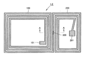
図1に示すように、ICカード・タグ用アンテナ回路構成体の一例としてのICカード・タグ用アンテナ回路構成体1は、第1のアンテナ回路パターン層100と、第2のアンテナ回路パターン層200とを備える。第1のアンテナ回路パターン層100と第2のアンテナ回路パターン層200とは、それぞれ渦巻状のパターンで形成され、接続部300によって電気的に接続されている。第1のアンテナ回路パターン層100の端部には他の回路部と接続するための接続領域101等が形成され、第2のアンテナ回路パターン層200の端部にはICチップを搭載するためのはんだ付け領域201等が形成されている。
As shown in FIG. 1, an IC card / tag
図2に示すように、第1のアンテナ回路パターン層100は、アルミニウム箔層12から構成されている。アルミニウム箔層12は、主成分としてアルミニウムを含む電気導電体である。第2のアンテナ回路パターン層200は、アルミニウム箔層12と、このアルミニウム箔層12の表面上に形成されたニッケルめっき層13を介在して、アルミニウム箔層12の表面を覆うように形成された銅めっき層14とから構成されている。第2のアンテナ回路パターン層200の表面を形成する銅めっき層14は、アルミニウムと異なる銅を主成分として含む電気導電体である。接続部300も、アルミニウム箔層12と、このアルミニウム箔層12の表面上に形成されたニッケルめっき層13を介在して、アルミニウム箔層12の表面を覆うように形成された銅めっき層14とから構成されている。このように構成された第1のアンテナ回路パターン層100と第2のアンテナ回路パターン層200と接続部300は、樹脂フィルム基材11の一方側の表面上に接着剤層(図示せず)を介在して所定のパターンに従って形成されている。
As shown in FIG. 2, the first antenna
次に、この発明の実施の形態1としてのICカード・タグ用アンテナ回路構成体の製造方法について説明する。図3〜図9はこの発明の実施の形態1としてのICカード・タグ用アンテナ回路構成体の製造工程を示す部分断面図である。なお、図3〜図9は、図1のA−A線の方向から見た部分断面を示している。
Next, a method for manufacturing an IC card / tag antenna circuit assembly as
図3に示すように、樹脂フィルム基材11の一方側の表面に接着剤層(図示せず)を形成し、この接着剤層によって樹脂フィルム基材11の一方側の表面に、アルミニウムを主成分とするアルミニウム箔120を固着する。このようにして、アルミニウム箔120と樹脂フィルム基材11との積層体を準備する。次に、第1のアンテナ回路パターンと第2のアンテナ回路パターンの仕様に従った所定の二つの渦巻状パターンを有するように第1のレジスト層としてレジストインク層15をアルミニウム箔120の表面上に印刷する。印刷後、レジストインク層15の硬化処理を行なう。
As shown in FIG. 3, an adhesive layer (not shown) is formed on one surface of the
図4に示すように、レジストインク層15をマスクとして用いてアルミニウム箔120の一部をエッチングすることにより、アルミニウム箔層12を形成する。
As shown in FIG. 4, the
その後、図5に示すように、レジストインク層15を剥離する。
Thereafter, as shown in FIG. 5, the resist
そして、図6に示すように、アルミニウム箔層12の表面を覆うようにニッケルめっき層13を形成し、さらにニッケルめっき層13を介在してアルミニウム箔層12の表面を覆うように、アルミニウムと異なる銅を主成分とする銅めっき層14を形成する。
And as shown in FIG. 6, it differs from aluminum so that the
さらに、図7に示すように、銅めっき層14の一部の表面を覆うように第2のレジスト層として、接続部300を含む第2のアンテナ回路パターンの仕様に従った所定の一つの渦巻状パターンを有するレジストインク層15を形成する。形成後、レジストインク層15の硬化処理を行なう。
Further, as shown in FIG. 7, a predetermined one spiral according to the specification of the second antenna circuit pattern including the
図8に示すように、レジストインク層15をマスクとして用いて銅めっき層14とニッケルめっき層13の一部をエッチングする。
As shown in FIG. 8, a part of the
最後に、図9に示すようにレジストインク層15を除去することにより、図2に示すように、アルミニウム箔層12からなる第1のアンテナ回路パターン層100と、アルミニウム箔層12とニッケルめっき層13と銅めっき層14とからなる第2のアンテナ回路パターン層200および接続部300とが形成される。このようにして本発明のICカード・タグ用アンテナ回路構成体1が完成する。
Finally, by removing the resist
(実施の形態2)
図1は、この発明のもう1つの実施の形態に従ったICカード・タグ用アンテナ回路構成体の平面図、図10は図1のA−A線の方向から見た部分断面図である。
(Embodiment 2)
FIG. 1 is a plan view of an antenna circuit structure for an IC card / tag according to another embodiment of the present invention, and FIG. 10 is a partial sectional view seen from the direction of line AA in FIG.
図1に示すように、ICカード・タグ用アンテナ回路構成体の一例としてのICカード・タグ用アンテナ回路構成体2は、第1のアンテナ回路パターン層100と、第2のアンテナ回路パターン層200とを備える。第1のアンテナ回路パターン層100と第2のアンテナ回路パターン層200とは、それぞれ渦巻状のパターンで形成され、接続部300によって電気的に接続されている。第1のアンテナ回路パターン層100の端部には他の回路部と接続するための接続領域101等が形成され、第2のアンテナ回路パターン層200の端部にはICチップを搭載するためのはんだ付け領域201等が形成されている。
As shown in FIG. 1, an IC card / tag antenna circuit structure 2 as an example of an IC card / tag antenna circuit structure includes a first antenna
図10に示すように、第1のアンテナ回路パターン層100は、アルミニウム箔層22から構成されている。アルミニウム箔層22は、主成分としてアルミニウムを含む電気導電体である。第2のアンテナ回路パターン層200は、銅めっき層24から構成されている。銅めっき層24は、アルミニウムと異なる銅を主成分として含む電気導電体である。接続部300は、アルミニウム箔層22と、このアルミニウム箔層22の表面上に形成されたニッケルめっき層23を介在して、アルミニウム箔層22の表面を覆うように形成された銅めっき層24とから構成されている。このように構成された第1のアンテナ回路パターン層100と第2のアンテナ回路パターン層200と接続部300は、樹脂フィルム基材11の一方側の表面上に接着剤層(図示せず)を介在して所定のパターンに従って形成されている。
As shown in FIG. 10, the first antenna
次に、この発明の実施の形態2としてのICカード・タグ用アンテナ回路構成体の製造方法について説明する。図11〜図18はこの発明の実施の形態2としてのICカード・タグ用アンテナ回路構成体の製造工程を示す部分断面図である。なお、図11〜図18は、図1のA−A線の方向から見た部分断面を示している。 Next, a method for manufacturing an IC card / tag antenna circuit assembly as Embodiment 2 of the present invention will be described. FIGS. 11 to 18 are partial cross-sectional views showing manufacturing steps of an IC card / tag antenna circuit assembly as a second embodiment of the present invention. In addition, FIGS. 11-18 has shown the partial cross section seen from the direction of the AA line of FIG.
図11に示すように、樹脂フィルム基材21の一方側の表面に接着剤層(図示せず)を形成し、この接着剤層によって樹脂フィルム基材21の一方側の表面に、アルミニウムを主成分とするアルミニウム箔220を固着する。このようにして、アルミニウム箔220と樹脂フィルム基材21との積層体を準備する。次に、第1のアンテナ回路パターンの仕様に従った所定の一つの渦巻状パターンを有するように第1のレジスト層としてレジストインク層25をアルミニウム箔220の表面上に印刷する。印刷後、レジストインク層25の硬化処理を行なう。
As shown in FIG. 11, an adhesive layer (not shown) is formed on one surface of the
図12に示すように、レジストインク層25をマスクとして用いてアルミニウム箔220の一部をエッチングすることにより、アルミニウム箔層22を形成する。
As shown in FIG. 12, the
その後、図13に示すように、レジストインク層25を剥離する。
Thereafter, as shown in FIG. 13, the resist
そして、図14に示すように、アルミニウム箔層22の表面を覆うようにニッケルめっき層23を形成する。
And as shown in FIG. 14, the
さらに、図15に示すように、ニッケルめっき層23を介在してアルミニウム箔層22の表面を覆うように、かつ、樹脂フィルム基材21の表面上に、アルミニウムと異なる銅を主成分とする銅めっき層24を形成する。
Further, as shown in FIG. 15, copper whose main component is copper different from aluminum is provided on the surface of the
次に、図16に示すように、接続部300を含む第2のアンテナ回路パターンの仕様に従った所定の一つの渦巻状パターンを有する第2のレジスト層として、レジストインク層25を銅めっき層24の表面上に印刷する。印刷後、レジストインク層25の硬化処理を行なう。
Next, as shown in FIG. 16, as a second resist layer having a predetermined spiral pattern according to the specifications of the second antenna circuit pattern including the
図17に示すように、レジストインク層25をマスクとして用いて銅めっき層24とニッケルめっき層23の一部をエッチングする。
As shown in FIG. 17, the
最後に、図18に示すようにレジストインク層25を除去することにより、図10に示すように、アルミニウム箔層22からなる第1のアンテナ回路パターン層100と、銅めっき層24からなる第2のアンテナ回路パターン層200と、アルミニウム箔層22とニッケルめっき層23と銅めっき層24とからなる接続部300とが形成される。このようにして本発明のICカード・タグ用アンテナ回路構成体2が完成する。
Finally, by removing the resist
上記の実施の形態1と2においてアルミニウム箔層12、22を形成するために用いられるアルミニウム箔120、220の厚みは5μm以上100μm以下であるのが好ましい。アルミニウム箔は、上記の厚みを満たせば、公知の純アルミニウム箔、アルミニウム合金箔であってもよい。具体的には、純アルミニウム(JIS(AA)1000系、たとえば1N30、1N70等)、Al−Mn系(JIS(AA)3000系、たとえば3003、3004等)、Al−Mg系(JIS(AA)5000系)、Al−Fe系(JIS(AA)8000系、たとえば8021、8079等)等の箔を採用することができる。アルミニウム箔に含まれる鉄(Fe)、シリコン(Si)、銅(Cu)、ニッケル(Ni)、クロム(Cr)、チタン(Ti)、ジルコニウム(Zr)、亜鉛(Zn)、マンガン(Mn)、マグネシウム(Mg)、ガリウム(Ga)等の成分については、JIS等で規定されている公知の含有量の範囲内であれば差し支えない。しかしながら、これらの添加元素または不可避的不純物元素は、アルミニウム箔の強度、電気抵抗を大幅に左右するので、要求性能に応じて適宜選択または制御すればよい。また、アルミニウム箔は熱処理によってもその強度、電気抵抗が変化するので、必要に応じて硬質材、半硬質材、軟質材を使い分ければよい。また、アルミニウム箔には、必要に応じて、脱脂・洗浄、アンカーコート、プライマー、表面処理等を施すこともできる。 The thickness of the aluminum foils 120 and 220 used for forming the aluminum foil layers 12 and 22 in the first and second embodiments is preferably 5 μm or more and 100 μm or less. The aluminum foil may be a known pure aluminum foil or aluminum alloy foil as long as the above thickness is satisfied. Specifically, pure aluminum (JIS (AA) 1000 series, such as 1N30, 1N70, etc.), Al-Mn series (JIS (AA) 3000 series, such as 3003, 3004 etc.), Al-Mg series (JIS (AA)). 5000-based), Al-Fe-based (JIS (AA) 8000-based, for example, 8021, 8079, etc.) foils can be employed. Iron (Fe), silicon (Si), copper (Cu), nickel (Ni), chromium (Cr), titanium (Ti), zirconium (Zr), zinc (Zn), manganese (Mn) contained in the aluminum foil, About components, such as magnesium (Mg) and gallium (Ga), if it exists in the range of the well-known content prescribed | regulated by JIS etc., it does not interfere. However, these additive elements or unavoidable impurity elements greatly affect the strength and electrical resistance of the aluminum foil, and may be appropriately selected or controlled according to the required performance. In addition, since the strength and electrical resistance of aluminum foil change by heat treatment, a hard material, a semi-hard material, and a soft material may be properly used as necessary. In addition, the aluminum foil can be subjected to degreasing / washing, anchor coating, primer, surface treatment and the like, if necessary.
上記の実施の形態1と2においてニッケルめっき層13、23の形成は、次のようにして行われるのが好ましい。ニッケルめっき層13、23の形成は、電解めっき法、または、無電解めっき法のいずれを採用しても可能であるが、線幅が0.5μm程度の細線からなるアンテナ回路パターン層の一部を構成するために均一な膜厚のめっき層を形成する方法としては、無電解めっき法を採用するのがより好ましい。めっき液は市販のめっき液を適宜使用すればよい。 In the first and second embodiments, the nickel plating layers 13 and 23 are preferably formed as follows. The nickel plating layers 13 and 23 can be formed by either electrolytic plating or electroless plating, but a part of the antenna circuit pattern layer formed of a thin wire having a line width of about 0.5 μm. As a method for forming a plating layer having a uniform film thickness in order to form the film, it is more preferable to employ an electroless plating method. A commercially available plating solution may be appropriately used as the plating solution.
無電解めっき法を採用したニッケルめっき層の形成の具体例としては、例えば、硫酸ニッケル20g/リットル、次亜りん酸ナトリウム25g/リットル、乳酸5g/リットルおよびクエン酸ナトリウム5g/リットルを主成分とする無電解めっき液を、pH4.0〜5.0、温度 80〜90℃となるように調整した後、所望の厚みのめっき層が得られるまでの時間、ニッケルめっき層が施される被対象物を上記の無電解めっき液に浸漬すればよい。 Specific examples of the formation of the nickel plating layer employing the electroless plating method include, for example, nickel sulfate 20 g / liter, sodium hypophosphite 25 g / liter, lactic acid 5 g / liter, and sodium citrate 5 g / liter as main components. After the electroless plating solution is adjusted to have a pH of 4.0 to 5.0 and a temperature of 80 to 90 ° C., the time until a plating layer having a desired thickness is obtained, and the object to which the nickel plating layer is applied What is necessary is just to immerse an object in said electroless-plating liquid.
電解めっき法を採用してニッケルめっき層を形成する場合、電解ニッケルめっき液として、硫酸ニッケル、塩化ニッケルおよびホウ酸を主成分とするワット液を用いて、公知の電解めっき法に従ってニッケルめっき層を形成すればよい。 When the nickel plating layer is formed by employing the electrolytic plating method, the nickel plating layer is formed according to a known electrolytic plating method using a Watt solution mainly composed of nickel sulfate, nickel chloride and boric acid as the electrolytic nickel plating solution. What is necessary is just to form.
なお、ニッケルめっき層としては、特に成分としてニッケルとりんを含むめっき層を形成するのが一般的である。このとき、めっき層に含まれるりん含有量を2〜15質量%にするのが好ましく、上記の範囲にりん含有量を設定すると、より強固なニッケルめっき層を形成することができる。 As the nickel plating layer, a plating layer containing nickel and phosphorus as components is generally formed. At this time, it is preferable that the phosphorus content contained in the plating layer is 2 to 15% by mass. If the phosphorus content is set in the above range, a stronger nickel plating layer can be formed.
上記の実施の形態1と2において銅めっき層14、24の形成は、次のようにして行われるのが好ましい。銅めっき層14、24の形成は、電解めっき法、または、無電解めっき法のいずれを採用しても可能である。めっき液は、シアン化銅系、硫酸銅系、ピロりん酸銅系等の市販の銅めっき液を適宜使用すればよい。 In the first and second embodiments, the copper plating layers 14 and 24 are preferably formed as follows. The copper plating layers 14 and 24 can be formed by either electrolytic plating or electroless plating. As the plating solution, a commercially available copper plating solution such as a copper cyanide type, a copper sulfate type, or a copper pyrophosphate type may be appropriately used.
無電解めっき法を採用した銅めっき層の形成の具体例としては、例えば、硫酸銅10g/リットル、エチレンジアミンテトラ酢酸(EDTA)30g/リットルおよびホルマリン10g/リットルを主成分とする無電解めっき液を、pH12.5前後、温度20〜25℃となるように調整した後、所望の厚みのめっき層が得られるまでの時間、銅めっき層が施される被対象物を上記の無電解めっき液に浸漬すればよい。 Specific examples of the formation of a copper plating layer employing an electroless plating method include, for example, an electroless plating solution mainly composed of copper sulfate 10 g / liter, ethylenediaminetetraacetic acid (EDTA) 30 g / liter and formalin 10 g / liter. After adjusting so that it may become about pH 12.5 and temperature 20-25 degreeC, it is time until a plating layer of desired thickness is obtained, The target object to which a copper plating layer is given to said electroless-plating liquid What is necessary is just to immerse.
電解めっき法を採用した銅めっき層の形成の具体例としては、硫酸180〜200g/リットルおよび硫酸銅50〜60g/リットルを主成分とする電解めっき液中で、液温20〜22℃、電流密度1.5〜2.0A/cm2の条件で、所望の厚みのめっき層が得られるまでの時間、銅めっき層が形成される被対象物を上記の電解めっき液中に浸漬した状態で電解を行えばよい。 As a specific example of the formation of the copper plating layer employing the electrolytic plating method, in an electrolytic plating solution mainly composed of 180 to 200 g / liter of sulfuric acid and 50 to 60 g / liter of copper sulfate, the liquid temperature is 20 to 22 ° C., the current is In a state where the object on which the copper plating layer is formed is immersed in the electrolytic plating solution for a time until a plating layer having a desired thickness is obtained under conditions of a density of 1.5 to 2.0 A / cm 2. What is necessary is just to perform electrolysis.
なお、上述した各めっき層の形成に際して、公知の前処理または後処理を適宜行ってもよい。例えば、銅めっき層を形成するための前処理として、三酸化クロムを主成分とするサージェント浴を用いて下地層としてのクロムめっき層を形成してもよい。 In addition, when forming each plating layer mentioned above, you may perform well-known pre-processing or post-processing suitably. For example, as a pretreatment for forming a copper plating layer, a chromium plating layer as a base layer may be formed using a Sargent bath mainly composed of chromium trioxide.
本発明のICカード・タグ用アンテナ回路構成体の基材として用いられる樹脂フィルムは、ポリエチレン(高密度ポリエチレン、低密度ポリエチレン、線状低密度ポリエチレン等)、ポリプロピレン、ポリエチレンテレフタレート、ポリエチレンナフタレート、ナイロン、塩化ビニル、低収縮性ポリエチレンテレフタレート(PET)フィルムおよび低収縮性ポリエチレンナフタレート(PEN)フィルム等から選ばれる少なくとも1種であるのが好ましく、これらの中でも低収縮性ポリエチレンテレフタレート(PET)フィルムおよび低収縮性ポリエチレンナフタレート(PEN)フィルムから選ばれる少なくとも1種であるのが好ましい。この樹脂フィルムの厚みは15〜70μmの範囲内であるのが好ましく、より好ましくは20〜50μmの範囲内である。基材の厚みが15μm未満では、回路パターン層を形成するアルミニウム箔との積層体の剛性が不足するため、各製造工程での作業性に問題が生じる。一方、基材の厚みが70μmを超える場合には、後述するクリンピング処理を確実に行なうことができないおそれがある。 The resin film used as the base material of the antenna circuit component for IC card / tag of the present invention is polyethylene (high density polyethylene, low density polyethylene, linear low density polyethylene, etc.), polypropylene, polyethylene terephthalate, polyethylene naphthalate, nylon. And at least one selected from vinyl chloride, low-shrinkage polyethylene terephthalate (PET) film, low-shrinkage polyethylene naphthalate (PEN) film, and the like. Among these, low-shrinkage polyethylene terephthalate (PET) film and It is preferably at least one selected from low-shrinkage polyethylene naphthalate (PEN) films. The thickness of the resin film is preferably in the range of 15 to 70 μm, more preferably in the range of 20 to 50 μm. If the thickness of the base material is less than 15 μm, the laminate is insufficiently rigid with the aluminum foil forming the circuit pattern layer, which causes a problem in workability in each manufacturing process. On the other hand, when the thickness of the substrate exceeds 70 μm, the crimping process described later may not be performed reliably.
回路パターン層を形成するためのアルミニウム箔と、基材としての樹脂フィルムとの間の接着は、エポキシ樹脂を含有するポリウレタン(PU)系接着剤を用いたドライラミネーションによるのが好ましい。エポキシ樹脂を含有するポリウレタン系接着剤としては東洋モートン社製AD506、AD503、AD76−P1等を採用することができ、硬化剤としては同社製CAT−10を接着剤:硬化剤=2〜12:1の比率で配合して使用すればよい。通常のエポキシ樹脂を含有しないポリウレタン系接着剤を用いた場合には、回路パターン層を形成するためのエッチング処理中や、ICチップを実装するときにデラミネーション(剥離)が生じやすくなる。これは、エポキシ樹脂を含有しないポリウレタン系接着剤が耐薬品性や耐熱性に劣るからである。 Adhesion between the aluminum foil for forming the circuit pattern layer and the resin film as the substrate is preferably by dry lamination using a polyurethane (PU) -based adhesive containing an epoxy resin. Toyo Morton's AD506, AD503, AD76-P1, etc. can be used as the polyurethane-based adhesive containing an epoxy resin, and CAT-10 made by the company is used as the curing agent: Adhesive: Curing agent = 2 to 12: What is necessary is just to mix | blend and use by the ratio of 1. When a polyurethane adhesive that does not contain an ordinary epoxy resin is used, delamination (peeling) is likely to occur during an etching process for forming a circuit pattern layer or when an IC chip is mounted. This is because a polyurethane adhesive not containing an epoxy resin is inferior in chemical resistance and heat resistance.
基材としての樹脂フィルムの上に回路パターン層を形成するためのアルミニウム箔を接着させるためには、エポキシ樹脂を含有するポリウレタン系接着剤を乾燥後において重量で1〜15g/m2程度塗布するのが好ましい。この塗布量が1g/m2未満では、アルミニウム箔の接着力が不足し、15g/m2を超える場合には、クリンピング加工を阻害するとともに、製造コストの上昇を招く。 In order to adhere an aluminum foil for forming a circuit pattern layer on a resin film as a base material, a polyurethane-based adhesive containing an epoxy resin is applied in a weight of about 1 to 15 g / m 2 after drying. Is preferred. When the coating amount is less than 1 g / m 2 , the adhesive strength of the aluminum foil is insufficient, and when it exceeds 15 g / m 2 , crimping is hindered and the manufacturing cost is increased.
この発明の製造方法において用いられるレジストインクは特に限定されないが、分子中に少なくとも1個のカルボキシル基を有するアクリルモノマーとアルカリ可溶性樹脂とを主成分とする紫外線硬化型レジストインクを用いるのが好ましい。このレジストインクは、グラビア印刷が可能であり、耐酸性を有し、かつアルカリによって容易に剥離除去することが可能であるので、連続大量生産に適している。このレジストインクを用いて銅箔に所定の回路パターンでグラビア印刷を施し、紫外線を照射して硬化させた後、通常の方法に従って、たとえば塩化第二鉄等による銅箔の酸エッチング、水酸化ナトリウム等のアルカリによるレジストインク層の剥離除去を行なうことによって、回路パターン層を形成することができる。 The resist ink used in the production method of the present invention is not particularly limited, but it is preferable to use an ultraviolet curable resist ink mainly composed of an acrylic monomer having at least one carboxyl group in the molecule and an alkali-soluble resin. This resist ink is suitable for continuous mass production because it can be gravure printed, has acid resistance, and can be easily removed by alkali. Using this resist ink, the copper foil is subjected to gravure printing with a predetermined circuit pattern and cured by irradiating with ultraviolet rays. Then, according to a normal method, for example, acid etching of the copper foil with ferric chloride or the like, sodium hydroxide The circuit pattern layer can be formed by removing and removing the resist ink layer with an alkali such as alkali.
分子中に少なくとも1個のカルボキシル基を有するアクリルモノマーとしては、たとえば、2−アクリロイルオキシエチルフタル酸、2−アクリロイルオキシエチルコハク酸、2−アクリロイルオキシエチルヘキサヒドロフタル酸、2−アクリロイルオキシプロピルフタル酸、2−アクリロイルオキシプロピルテトラヒドロフタル酸、2−アクリロイルオキシプロピルヘキサヒドロフタル酸等が挙げられ、これらのうち、単独のアクリルモノマー、またはいくつかのアクリルモノマーを混合したものを使用することができる。上記のアルカリ可溶性樹脂としては、たとえば、スチレン−マレイン酸樹脂、スチレン−アクリル樹脂、ロジン−マレイン酸樹脂等が挙げられる。 Examples of acrylic monomers having at least one carboxyl group in the molecule include 2-acryloyloxyethyl phthalic acid, 2-acryloyloxyethyl succinic acid, 2-acryloyloxyethyl hexahydrophthalic acid, 2-acryloyloxypropyl phthalate. Acid, 2-acryloyloxypropyltetrahydrophthalic acid, 2-acryloyloxypropylhexahydrophthalic acid, and the like. Among these, a single acrylic monomer or a mixture of several acrylic monomers can be used. . Examples of the alkali-soluble resin include styrene-maleic acid resin, styrene-acrylic resin, and rosin-maleic acid resin.
レジストインクには、上記の成分の他に、アルカリ剥離性を阻害しない程度に通常の単官能アクリルモノマー、多官能アクリルモノマー、プレポリマーを添加することができ、光重合開始剤、顔料、添加剤、溶剤等を適宜添加して作製することができる。光重合開始剤としては、ベンゾフェノンおよびその誘導体、ベンジル、ベンゾイン、およびそのアルキルエーテル、チオキサントンおよびその誘導体、ルシリンPTO、チバスペシャリティケミカルズ製イルガキュア、フラッテリ・ランベルティ製エサキュア等が挙げられる。顔料としては、パターンが見やすいように着色顔料を添加する他、シリカ、タルク、クレー、硫酸バリウム、炭酸カルシウム等の体質顔料を併用することができる。特にシリカは、紫外線硬化型レジストインクを付けたまま、銅箔を巻き取る場合には、ブロッキング防止に効果がある。添加剤としては、2−ターシャリーブチルハイドロキノン等の重合禁止剤、シリコン、フッ素化合物、アクリル重合物等の消泡剤、レベリング剤があり、必要に応じて適宜添加する。溶剤としては酢酸エチル、エタノール、変性アルコール、イソプロピルアルコール、トルエン、MEK等が挙げられ、これらのうち、溶剤を単独、または混合して用いることができる。溶剤は、グラビア印刷の後、熱風乾燥等でレジストインク層から蒸発させることが好ましい。 In addition to the above components, normal monofunctional acrylic monomers, polyfunctional acrylic monomers, and prepolymers can be added to the resist ink to such an extent that alkali peelability is not impaired. It can be prepared by appropriately adding a solvent or the like. Examples of the photopolymerization initiator include benzophenone and derivatives thereof, benzyl, benzoin and alkyl ethers thereof, thioxanthone and derivatives thereof, lucillin PTO, Irgacure manufactured by Ciba Specialty Chemicals, Esacure manufactured by Fratelli Lamberti, and the like. As the pigment, a coloring pigment is added so that the pattern is easy to see, and extender pigments such as silica, talc, clay, barium sulfate, calcium carbonate and the like can be used in combination. In particular, silica is effective in preventing blocking when a copper foil is wound with an ultraviolet curable resist ink attached. Additives include polymerization inhibitors such as 2-tertiary butyl hydroquinone, antifoaming agents such as silicon, fluorine compounds, and acrylic polymers, and leveling agents, which are added as necessary. Examples of the solvent include ethyl acetate, ethanol, denatured alcohol, isopropyl alcohol, toluene, MEK, and the like. Among these, the solvents can be used alone or in combination. The solvent is preferably evaporated from the resist ink layer by hot air drying after gravure printing.
このようにして得られた本発明のICカード・タグ用アンテナ回路構成体の実施の形態においては、アルミニウムと銅の異種の金属からなる複数のアンテナ回路パターン層が基材の同一表面上に形成されているので、第1と第2のアンテナ回路パターン層は、アルミニウムと銅の利点をそれぞれ活かした特性を備えるとともに、第1のアンテナ回路パターン層は銅の欠点を補うことが可能なアルミニウムを用いて形成され、第2のアンテナ回路パターン層はアルミニウムの欠点を補うことが可能な銅を用いて形成することができる。これにより、一つの基材の表面上に種々の特性を有する複数のアンテナ回路パターン層を形成することができ、種々の特性を併せ持つことが可能なICカード・タグ用アンテナ回路構成体を得ることができる。 In the embodiment of the antenna circuit structure for IC card / tag of the present invention thus obtained, a plurality of antenna circuit pattern layers made of different metals of aluminum and copper are formed on the same surface of the substrate. Therefore, the first and second antenna circuit pattern layers have characteristics utilizing the advantages of aluminum and copper, respectively, and the first antenna circuit pattern layer is made of aluminum that can compensate for the disadvantages of copper. The second antenna circuit pattern layer can be formed using copper capable of compensating for the defects of aluminum. Thereby, a plurality of antenna circuit pattern layers having various characteristics can be formed on the surface of one base material, and an antenna circuit structure for IC card / tag capable of having various characteristics can be obtained. Can do.
特に、この発明のICカード・タグ用アンテナ回路構成体の実施の形態においては、クリンピング等の機械加工が可能で変色され難い、アルミニウムを用いて形成された第1のアンテナ回路パターン層100と、はんだ加工が可能で導電性に優れた、銅を用いて形成された第2のアンテナ回路パターン層200とを一つの基材の表面上に備えたICカード・タグ用アンテナ回路構成体を得ることができる。また、エッチングによってアンテナ回路パターン層を形成する場合、銅の方がアルミニウムよりもエッチング精度に優れているので、相対的に高い精度を要する回路を第2のアンテナ回路パターン層200で形成し、特に高い精度が要求されない回路を第1のアンテナ回路パターン層100で形成することができる。さらに、アルミニウムは銅に比べて高い耐候性を有するので、一つのICカード・タグ用アンテナ回路構成体において外気の影響を受けやすい箇所に配置される回路を第1のアンテナ回路パターン層100で形成し、他の箇所に配置される回路を第2のアンテナ回路パターン層200で形成することができる。
In particular, in the embodiment of the antenna circuit structure for IC card / tag according to the present invention, a first antenna
このようにアンテナ回路パターン層を異種の金属を用いて形成することによって、種々の特性を有する複数のアンテナコイルを構成することができる。 In this way, by forming the antenna circuit pattern layer using different kinds of metals, a plurality of antenna coils having various characteristics can be configured.
さらに、この発明のICカード・タグ用アンテナ回路構成体において、第1のアンテナ回路パターン層100と第2のアンテナ回路パターン層200とが電気的に接続された接続部を備えることにより、一つの基材の表面上に種々の特性を有する複数のアンテナ回路パターン層を形成することができ、これらの複数のアンテナ回路パターン層が電気的に接続されて、種々の特性を併せ持つことが可能なICカード・タグ用アンテナ回路構成体を得ることができる。たとえば、世界的に広く流通する商品に貼り付けるICタグにおいて、ICタグに記憶された情報を読み取るための種々のリーダー機器に対応することができるようにアンテナコイルを二重にするために、本発明のように異種の金属を用いて形成されたアンテナ回路パターン層を備える回路構成体を適用することができる。
Furthermore, in the antenna circuit structure for an IC card / tag according to the present invention, by providing a connection portion in which the first antenna
なお、上記の実施の形態では、本発明の回路構成体の例としてICカード・タグ用アンテナ回路構成体を挙げて説明したが、ICカード・タグ用アンテナ回路構成体に限定されるものではなく、種々の電子機器に関連する回路を構成する装置や物品に本発明の回路構成体を適用することができる。 In the above embodiment, the IC card / tag antenna circuit structure is described as an example of the circuit structure of the present invention. However, the present invention is not limited to the IC card / tag antenna circuit structure. The circuit structure of the present invention can be applied to devices and articles constituting circuits related to various electronic devices.
今回開示された実施の形態はすべての点で例示であって制限的なものではないと考慮されるべきである。本発明の範囲は以上の実施の形態ではなく、特許請求の範囲によって示され、特許請求の範囲と均等の意味および範囲内でのすべての修正と変形を含むものであることが意図される。 It should be considered that the embodiments disclosed herein are illustrative and non-restrictive in every respect. The scope of the present invention is shown not by the above embodiments but by the scope of the claims, and is intended to include all modifications and variations within the meaning and scope equivalent to the scope of the claims.
1,2:ICカード・タグ用アンテナ回路構成体、11,21:樹脂フィルム基材、12,22:アルミニウム箔層、13,23:ニッケルめっき層、14,24:銅めっき層、15,25:レジストインク層、100:第1のアンテナ回路パターン層、200:第2のアンテナ回路パターン層、120,220:アルミニウム箔、300:接続部。
DESCRIPTION OF
Claims (7)
この基材の表面の上に形成されたアンテナ回路パターン層とを備え、
前記アンテナ回路パターン層は、第1の金属を主成分とする電気導電体を有し、渦巻状のパターンで形成された第1のアンテナ回路パターン層と、前記第1の金属と異なる第2の金属を主成分とする電気導電体を有し、渦巻状のパターンで形成された第2のアンテナ回路パターン層とを含む、ICカード・タグ用アンテナ回路構成体。 A base material containing a resin;
An antenna circuit pattern layer formed on the surface of the substrate;
The antenna circuit pattern layer, the first metal have a electrical conductor whose main component, a first antenna circuit pattern layer formed by spiral pattern, the first metal is different from the second metals have a electrical conductor whose main component, and a second antenna circuit pattern layer formed by spiral patterns, IC card tag antenna circuit structure.
前記金属箔の表面の上に、渦巻状のパターンで形成された第1のアンテナ回路パターンと第2のアンテナ回路パターンを有する第1のレジスト層を形成する工程と、
前記第1のレジスト層をマスクとして用いて前記金属箔の一部をエッチングすることによって、前記金属箔からなる金属パターン層を形成する工程と、
前記金属パターン層を形成した後に前記第1のレジスト層を除去する工程と、
前記金属パターン層を覆うように、前記第1の金属と異なる第2の金属を主成分とする金属めっき層を形成する工程と、
前記金属めっき層の表面の上に、前記第2のアンテナ回路パターンを有する第2のレジスト層を形成する工程と、
前記第2のレジスト層をマスクとして用いて前記金属めっき層の一部をエッチングすることによって、前記金属箔からなる第1のアンテナ回路パターン層と、前記金属箔と前記金属めっき層とからなる第2のアンテナ回路パターン層とを形成する工程とを備えた、ICカード・タグ用アンテナ回路構成体の製造方法。 Fixing a metal foil containing a first metal as a main component on the surface of a substrate containing a resin;
Forming a first resist layer having a first antenna circuit pattern and a second antenna circuit pattern formed in a spiral pattern on the surface of the metal foil;
Forming a metal pattern layer made of the metal foil by etching a part of the metal foil using the first resist layer as a mask;
Removing the first resist layer after forming the metal pattern layer;
Forming a metal plating layer mainly composed of a second metal different from the first metal so as to cover the metal pattern layer;
Forming a second resist layer having the second antenna circuit pattern on the surface of the metal plating layer;
A part of the metal plating layer is etched using the second resist layer as a mask, whereby a first antenna circuit pattern layer made of the metal foil, a first made of the metal foil and the metal plating layer is formed. A method of manufacturing an antenna circuit structure for an IC card / tag , comprising: a step of forming an antenna circuit pattern layer.
前記金属箔の表面の上に、渦巻状のパターンで形成された第1のアンテナ回路パターンを有する第1のレジスト層を形成する工程と、
前記第1のレジスト層をマスクとして用いて前記金属箔の一部をエッチングすることによって、前記金属箔からなる金属パターン層を形成する工程と、
前記金属パターン層を形成した後に前記第1のレジスト層を除去する工程と、
前記金属パターン層を覆い、かつ、前記基材の表面の上に、前記第1の金属と異なる第2の金属を主成分とする金属めっき層を形成する工程と、
前記金属めっき層の表面の上に、渦巻状のパターンで形成された第2のアンテナ回路パターンを有する第2のレジスト層を形成する工程と、
前記第2のレジスト層をマスクとして用いて前記金属めっき層の一部をエッチングすることによって、前記金属箔からなる第1のアンテナ回路パターン層と、前記金属めっき層からなる第2のアンテナ回路パターン層とを形成する工程とを備えた、ICカード・タグ用アンテナ回路構成体の製造方法。 Fixing a metal foil containing a first metal as a main component on the surface of a substrate containing a resin;
Forming a first resist layer having a first antenna circuit pattern formed in a spiral pattern on the surface of the metal foil;
Forming a metal pattern layer made of the metal foil by etching a part of the metal foil using the first resist layer as a mask;
Removing the first resist layer after forming the metal pattern layer;
Forming a metal plating layer mainly comprising a second metal different from the first metal on the surface of the base material, covering the metal pattern layer;
Forming a second resist layer having a second antenna circuit pattern formed in a spiral pattern on the surface of the metal plating layer;
Wherein by the second resist layer etching a portion of the metal plating layer using as a mask, a first antenna circuit pattern layer made of the metal foil, the second antenna circuit composed of the metal plating layer pattern A method of manufacturing an antenna circuit component for an IC card / tag , comprising a step of forming a layer.
Priority Applications (1)
| Application Number | Priority Date | Filing Date | Title |
|---|---|---|---|
| JP2007258233A JP4919921B2 (en) | 2007-10-02 | 2007-10-02 | Antenna circuit assembly for IC card / tag and manufacturing method thereof |
Applications Claiming Priority (1)
| Application Number | Priority Date | Filing Date | Title |
|---|---|---|---|
| JP2007258233A JP4919921B2 (en) | 2007-10-02 | 2007-10-02 | Antenna circuit assembly for IC card / tag and manufacturing method thereof |
Publications (2)
| Publication Number | Publication Date |
|---|---|
| JP2009088364A JP2009088364A (en) | 2009-04-23 |
| JP4919921B2 true JP4919921B2 (en) | 2012-04-18 |
Family
ID=40661365
Family Applications (1)
| Application Number | Title | Priority Date | Filing Date |
|---|---|---|---|
| JP2007258233A Expired - Fee Related JP4919921B2 (en) | 2007-10-02 | 2007-10-02 | Antenna circuit assembly for IC card / tag and manufacturing method thereof |
Country Status (1)
| Country | Link |
|---|---|
| JP (1) | JP4919921B2 (en) |
Cited By (1)
| Publication number | Priority date | Publication date | Assignee | Title |
|---|---|---|---|---|
| CN106982514A (en) * | 2017-05-09 | 2017-07-25 | 南方科技大学 | A kind of many material conducting wire plates of individual layer and preparation method |
Families Citing this family (1)
| Publication number | Priority date | Publication date | Assignee | Title |
|---|---|---|---|---|
| JP2012164912A (en) * | 2011-02-09 | 2012-08-30 | Toppan Printing Co Ltd | Wiring sheet for solar cell and manufacturing method of the wiring sheet for the solar cell, and solar cell module using the same |
Family Cites Families (5)
| Publication number | Priority date | Publication date | Assignee | Title |
|---|---|---|---|---|
| JPH0634440B2 (en) * | 1988-05-10 | 1994-05-02 | 電気化学工業株式会社 | Method for manufacturing printed wiring board |
| JPH08274123A (en) * | 1994-02-15 | 1996-10-18 | Denki Kagaku Kogyo Kk | Method for manufacturing conductor for hybrid integrated circuit substrate |
| JPH08330710A (en) * | 1995-06-05 | 1996-12-13 | Nippon Paint Co Ltd | Metal plating working method for electrode portion of printed wiring board |
| TWI296738B (en) * | 2001-03-29 | 2008-05-11 | Hitachi Chemical Co Ltd | |
| JP2005228795A (en) * | 2004-02-10 | 2005-08-25 | Konica Minolta Photo Imaging Inc | Coil, method and apparatus for manufacturing coil and inlet |
-
2007
- 2007-10-02 JP JP2007258233A patent/JP4919921B2/en not_active Expired - Fee Related
Cited By (1)
| Publication number | Priority date | Publication date | Assignee | Title |
|---|---|---|---|---|
| CN106982514A (en) * | 2017-05-09 | 2017-07-25 | 南方科技大学 | A kind of many material conducting wire plates of individual layer and preparation method |
Also Published As
| Publication number | Publication date |
|---|---|
| JP2009088364A (en) | 2009-04-23 |
Similar Documents
| Publication | Publication Date | Title |
|---|---|---|
| EP1477928A1 (en) | Antenna coil for IC card and manufacturing method thereof | |
| TWI530880B (en) | Antenna circuit constituent body for ic card/tag and method for manufacturing the same | |
| CN104427757A (en) | Surface-treated copper foil, copper foil with carrier, laminated board, printed wiring board, electronic machine and method for manufacturing printed wiring board | |
| KR101799177B1 (en) | Metal substrate with plating | |
| JP2015134953A (en) | Surface-treated copper foil, copper foil with carrier, printed wiring board, printed circuit board, copper-clad laminate, and method for producing printed wiring board | |
| KR100983682B1 (en) | Surface treatment method of copper foil for printed circuit, copper foil and electroplater thereof | |
| US20130068842A1 (en) | RFID Tag Structure Having Anti-Reuse Function and Manufacture Method Thereof | |
| KR100974373B1 (en) | Surface treatment method of copper foil for printed circuit, copper foil and electroplater thereof | |
| CN102265712B (en) | Method for forming electronic circuit | |
| JP4919921B2 (en) | Antenna circuit assembly for IC card / tag and manufacturing method thereof | |
| CN206490052U (en) | Nano metal base material for ultra fine-line FPC and COF material | |
| JP2002007990A (en) | Antenna coil for ic card and method of manufacturing the same | |
| JP4429611B2 (en) | Copper alloy composite foil, manufacturing method thereof, and high-frequency transmission circuit using the copper alloy composite foil | |
| JP2007141125A (en) | Antenna coil configuration for ic card, manufacturing method therefor, inlet sheet and ic card with the same | |
| WO2004070087A1 (en) | Composite copper foil, method for production thereof and high frequency transmission circuit using said composite copper foil | |
| JP3634774B2 (en) | Antenna coil for IC card | |
| WO2005004050A1 (en) | Conductive sheet for non-contact type ic card having built-in antenna and non-contact type ic card having built-in antenna | |
| JP2010028706A (en) | Circuit construct for ic card and tag, and manufacturing method therefor | |
| JP2004046360A (en) | Antenna coil configuration for ic card, manufacturing method therefor and ic card provided with the configuration | |
| JP6178360B2 (en) | Surface-treated copper foil, copper foil with carrier, method for producing printed circuit board, method for producing copper-clad laminate, and method for producing printed wiring board | |
| JP4011425B2 (en) | Antenna coil structure for IC card, method for manufacturing the same, and IC card having the same | |
| JP4969147B2 (en) | Manufacturing method of flexible printed wiring board | |
| JP2006007519A (en) | Composite film having circuit pattern and its manufacturing method | |
| JP4770420B2 (en) | Circuit board manufacturing method | |
| JP5561761B2 (en) | Manufacturing method of flexible printed wiring board |
Legal Events
| Date | Code | Title | Description |
|---|---|---|---|
| A621 | Written request for application examination |
Free format text: JAPANESE INTERMEDIATE CODE: A621 Effective date: 20100409 |
|
| A977 | Report on retrieval |
Free format text: JAPANESE INTERMEDIATE CODE: A971007 Effective date: 20110822 |
|
| A131 | Notification of reasons for refusal |
Free format text: JAPANESE INTERMEDIATE CODE: A131 Effective date: 20110830 |
|
| A521 | Written amendment |
Free format text: JAPANESE INTERMEDIATE CODE: A523 Effective date: 20111027 |
|
| TRDD | Decision of grant or rejection written | ||
| A01 | Written decision to grant a patent or to grant a registration (utility model) |
Free format text: JAPANESE INTERMEDIATE CODE: A01 Effective date: 20120124 |
|
| A01 | Written decision to grant a patent or to grant a registration (utility model) |
Free format text: JAPANESE INTERMEDIATE CODE: A01 |
|
| A61 | First payment of annual fees (during grant procedure) |
Free format text: JAPANESE INTERMEDIATE CODE: A61 Effective date: 20120131 |
|
| R150 | Certificate of patent or registration of utility model |
Free format text: JAPANESE INTERMEDIATE CODE: R150 |
|
| FPAY | Renewal fee payment (event date is renewal date of database) |
Free format text: PAYMENT UNTIL: 20150210 Year of fee payment: 3 |
|
| LAPS | Cancellation because of no payment of annual fees |